Band Bending Mechanism in CdO/Arsenene Heterostructure: A Potential Direct Z-scheme Photocatalyst
 Kai Ren
 Ruxin Zheng
 Jin Yu2
 - 1School of Mechanical and Electronic Engineering, Nanjing Forestry University, Nanjing, China
- 2School of Materials Science and Engineering, Southeast University, Nanjing, China
- 3School of Automotive and Transportation Engineering, Shenzhen Polytechnic, Shenzhen, China
For the few years, two-dimensional (2D) materials have aroused general focus. In order to expand the properties and application range of 2D materials, two different layered materials are usually combined into heterostructure through van der Waals (vdW) interaction. In this research, based on first-principles simulation, we propose CdO/Arsenene (CdO/As) vdW heterostructure as a semiconductor possessing a direct bandgap by 2.179 eV. Besides, the CdO/As vdW heterostructure presents type-II band alignment, which can be used as a remarkable photocatalyst. Importantly, the CdO/As heterostructure demonstrates a direct Z-type principle photocatalyst by exploring the band bending mechanism in the heterostructure. Furthermore, we calculated the light absorption characteristics of CdO/As vdW heterostructure by optical absorption spectrum and conversion efficiency of a novel solar-to-hydrogen efficiency (ηSTH) about 11.67%, which is much higher than that of other 2D photocatalysts. Our work can provide a theoretical guidance for the designing of Z-scheme photocatalyst.
Introduction
Since graphene was discovered in 2004 (Geim and Novoselov, 2007), it has continuously promoted the research and development of two-dimensional (2D) materials (Miró et al., 2014; Zhong et al., 2019a; He et al., 2019; Sun et al., 2019; Qi et al., 2020; Cui et al., 2021; Dai et al., 2021). After a long time of study on 2D materials, it was found that 2D material has extensive applications and is considered to be one of the most attractive and interesting material fields. All 2D materials show outstanding properties (Vahedi Fakhrabad et al., 2015; Xu et al., 2016; Zhong et al., 2017; Yuan et al., 2018; Sun and Schwingenschlögl, 2020; Luo et al., 2021), for example, the transition metal dichalcogenides (TMDs) materials have remarkable mechanical (Liu and Li, 2015), electronic (Zhang and Singh, 2009), optical (He et al., 2014), magnetic (Yuan et al., 2020) and thermal stability (Ding et al., 2016). Phosphorous possesses novel physical, chemical, optical properties and electrical conductivity (Li and Chen, 2014; Lee et al., 2016). Metal carbide (MXene) has excellent magnetic, thermoelectric properties and carrier mobility. In particular, Cr2TiC2 monolayer is a new 2D bipolar antiferromagnetic semiconductor and can be used as antiferromagnetic spin field effect transistor (He et al., 2018). The Hf2CO2 shows the excellent thermal conductivity (about 86.25–131.2 W m−1·K−1) along the armchair direction, and the expansion coefficient at room temperature is about 6.094 × 10⁻⁶ K−1 (Ren et al., 2021), and the carrier mobility reaches about 1,531.48 cm2/V·s (Cai et al., 2014). All these excellent performances explain that 2D materials show potential usage in photocatalysis, photovoltaic devices and heterostructure (Xu et al., 2015; Zhong et al., 2019b; Wang et al., 2020a; Sun et al., 2020b; Wang et al., 2020b; Sun and Schwingenschlögl, 2021a; Sun and Schwingenschlögl, 2021b; Lou et al., 2021; Sun et al., 2021; Zhu et al., 2021).
When TiO2 was found to be able to produce hydrogen (H2) from ultraviolet irradiated water in 1972 (Fujishima and Honda, 1972), many studies have been carried out using semiconductors as photocatalysts to decompose water (Yuan et al., 2016; Yang et al., 2017; Liu et al., 2018; Wang et al., 2020c; Yong et al., 2020). When the semiconductor is illuminated, the electrons are inspired to move from the valence band maximum (VBM) to the conduction band minimum (CBM), generating holes at the VBM (Maeda and Domen, 2007). However, recompositing rate of photogenerated electron–hole pairs is extraordinary increased due to the simultaneous reduction and oxidation reactions on the surface of monolayer material during water splitting. The popular way to solve this problem is to construct the type-II heterostructure (Ren et al., 2020a), which can effectively separate photogenerated electrons and holes. All 2D heterostructures are formed by van der Waals force (vdW) interaction, which produces more novel properties on the basis of original properties (Ren et al., 2019a), inducing more fantastic optical (Wang et al., 2018), interface properties (Ren et al., 2020b), carrier mobility (Luo et al., 2019) and Gibbs free energy (Ren et al., 2019b). In particular, the Z-scheme photocatalyst has become more and more popular because its special and efficient catalytic mechanism (Xu et al., 2018), such as As/PtS2 (Ren et al., 2020c), MoSe2/HfS2 (Wang et al., 2019), TiO2/CdS (Meng et al., 2017) etc., which are proved to possess novel catalytic performance by theoretical and experimental methods. Recently, it has been reported that a hexagonal monolayer semiconductor CdO was prepared by chemical spray pyrolysis and has got a lot of attention due to its outstanding mechanical and stability properties (Subramanyam et al., 1998; Zhuang and Hennig, 2013; Chaurasiya and Dixit, 2019; Chaurasiya et al., 2019; Ali et al., 2021). In addition, heterostructures based on CdO monolayer [such as ZnO/CdO (Sang et al., 2012), CdO/GaS (Zhao et al., 2021), etc.] also demonstrate unusual structural and electronic properties (Sang et al., 2012; Zhao et al., 2021). At the same time, Arsenene (As) is also a 2D material with many special properties, in particular, the band gap can be adjusted by applying external strain on the surface (Kamal and Ezawa, 2015). However, the heterostructures constructed by CdO and As are rarely reported, who share the same honeycomb hexagonal structure. Besides, considering that both CdO and As possess excellent electronic and optical characteristics, it is worth to explore the potential applications of heterostructure based on CdO and As monolayers.
In this study, performing first-principles calculations, the electronic characteristic of the CdO, As and CdO/As heterostructure are investigated with semiconductor nature. Furthermore, the CdO/As heterostructure has a type-II band structure to separate the photogenerated electrons and holes continuously. Interestingly, the bend bending style in CdO/As heterostructure demonstrates a potential direct Z-type photocatalyst and the optical performance is also addressed.
Materials and Methods
Considering the density functional theory (DFT), all simulation studies in this work were implemented by Vienna ab initio simulation software package (VASP) (Capelle, 2006; Togo et al., 2008; Togo and Tanaka, 2015). The core electron is described by projection enhanced wave potential (PAW) (Kresse and Joubert, 1999). The commutative relevant functional was explored, which is introduced by generalized gradient approximation (GGA) and Perdew–Burke–Ernzerhof (PBE) functional (Perdew et al., 1996; Grimme, 2006). At the same time, the weak dispersion force was considered by DFT-D3 with Grimme method (Grimme et al., 2010). Heyd–Scuseria–Ernzerhof mixed functional was used to obtain more accurate electronic and optical properties (Heyd et al., 2003). The parameters of 550 eV and 17 × 17 × 1 were used for the energy cut-off and the Monkhorst–Pack k-point grids in the first Brillouin zone. A vacuum space of 25 Å was used in the calculation to keep away from the interaction between adjacent mirror layers. The relaxation of the structure is simulated by conjugate gradient method. The Hellmann–Feynman force on each atom is limited to 0.01 eV Å−1.
According to the calculation method of solar-to-hydrogen efficiency (ηSTH) proposed by Yang etc (Xu et al., 2016) (ηSTH), where ηSTH = ηabs × ηcu, and ηabs, ηcu represents light absorption and carrier efficiency, respectively. Besides, the ηabs is calculated by:
where P(hω) is the solar energy flux by AM1.5G with the photon energy hω. Eg is the bandgap of studied materials. Furthermore, the ηcu is decided by:
where ΔG is 1.23 eV for the potential difference in water splitting. E is the photon energy using for water splitting, which is calculated by:
where χ(H2) and χ( O 2) are demonstrating the over potential for HER and OER, respectively.
Results and Discussion
First, the crystal structures of single-layer CdO and As was constructed and optimized. The side and top views of CdO and As monolayers are shown in Figures 1A,C, respectively. The lattice constants of CdO and As are calculated to be 3.684 and 3.607 Å, showing a small lattice mismatch of 2.11% for the CdO/As heterostructure, respectively. Besides, the energy band structures of monolayered CdO and As are calculated by HSE06 method, shown in Figures 1B,D, respectively. It can be clearly seen that monolayered CdO and As are semiconductors with the band gaps of 2.073 and 2.234 eV, respectively. For single-layer CdO, the CBM and VBM are located at Γ point, showing a direct bandgap structure. While the CBM of As monolayer is located between Γ and M points, the VBM exists at Γ points. Besides, the bond lengths of Cd–O and As–As in single-layer CdO and single-layer As were calculated to be 2.127 and 2.506 Å, respectively. Furthermore, all the above calculated results of CdO and As are almost consistent with previous investigations (Ren et al., 2020c; Zhao et al., 2021).
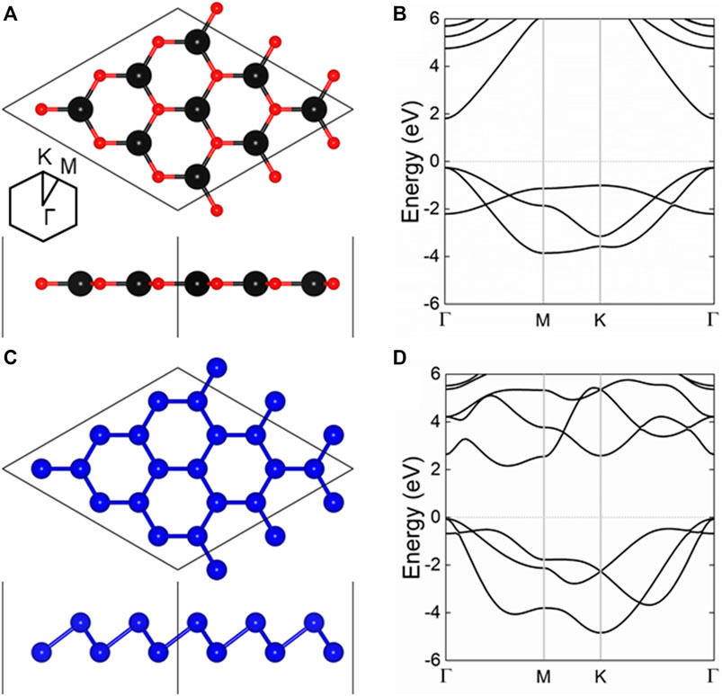
FIGURE 1. The (A,C) crystal structure and the (B,D) band structure of the (A,B) CdO and (C,D) As monolayers; the black, red and blue balls represent Cd, O and As atoms, respectively; the Fermi level is 0 shown as gray dashed line.
When monolayered CdO and As combine to form a heterostructure, 6 most representative highly symmetrical configurations have be considered. The side and top views of these 6 stacking combinations are shown in Figure 2. Among these 6 heterostructures, the most stable structure is determined by the binding energy (Ebinding) between single-layer CdO and As. The investigation shows that the smaller the binding energy is, the more stable the heterostructure is (Singh et al., 2015). The binding energy of CdO/As heterostructures is determined as following:
where ECdO/As, ECdO and EAs show the total energy of CdO/As heterostructure, single-layer CdO and As respectively. The binding energy of the most stable structure among the 6 stacked heterostructures is −36.64 meV/Å2 for the CA5 configuration, which is smaller than that in the vdW bonding in weak interlayer interactions in graphites of about −18 meV/Å2, shown as Figure 2E, suggesting that there is also a weak vdW force between CdO and As monolayers (Chen et al., 2013). The optimized bond length of Cd−O and As−As in CdO/As heterostructure are 2.082 and 2.504 Å, respectively, which just changed a little comparing with that in CdO and As monolayers, further showing the vdW interaction in CdO/As heterostructure. At the same time, we calculated the different interface distance (dH) of CdO/As vdW heterostructure, shown in Table 1. Furthermore, the discussed properties of the CdO/As vdW heterostructure is based on CA5 stacking configuration.
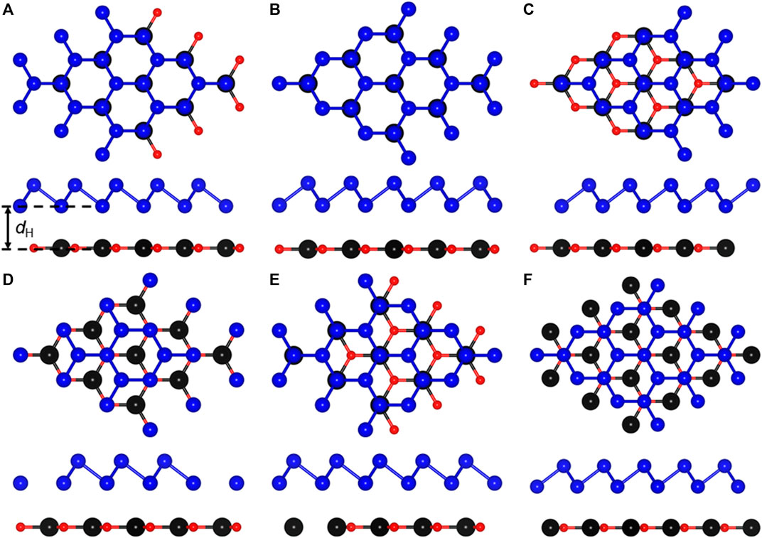
FIGURE 2. The CdO/As heterostructure constructing by (A) CA1, (B) CA2, (C) CA3, (D) CA4, (E) CA5 and (F) CA6 configurations.
TABLE 1. The binding energy (Ebinding, meV/Å2), interface distance (dH, Å) and the bond length (L, Å) of the different stacking style CdO/As heterostructure.
The projected band structure of CdO/As vdW heterostructure is calculated using HSE06 method, shown Figure 3A. Obviously, it can be clearly seen that CdO/As vdW heterostructure demonstrates the nature of semiconductor and shows a direct bandgap of 2.179 eV. Besides, it also can be seen that the CBM and VBM of CdO/As vdW heterostructure are located as Γ point contributed by As and CdO monolayers, respectively, which reveals a type-II band style. Then, such type-II band structure is further proved using the band-resolved charge densities for the CdO/As vdW heterostructure shown in Figure 3B. When the CdO/As vdW heterostructure is illuminated by the light, expressed by Figure 3C the photogenerated electrons will move from the VB of both CdO and As monolayers to the CB and the holes are keep. Then, by the assistance of the valence band offset (conduction band offset), the photogenerated electrons (holes) at CB (VB) of the CdO (As) layer migrate to the CB (VB) of the As (CdO) layer, thus, the photogenerated electrons and holes are effectively separated. Therefore, the gained type-II band alignment of CdO/As vdW heterostructure can effectively resist the recomposite of photogenerated electrons and holes, showing potential candidate use in application as a photocatalyst for water splitting.
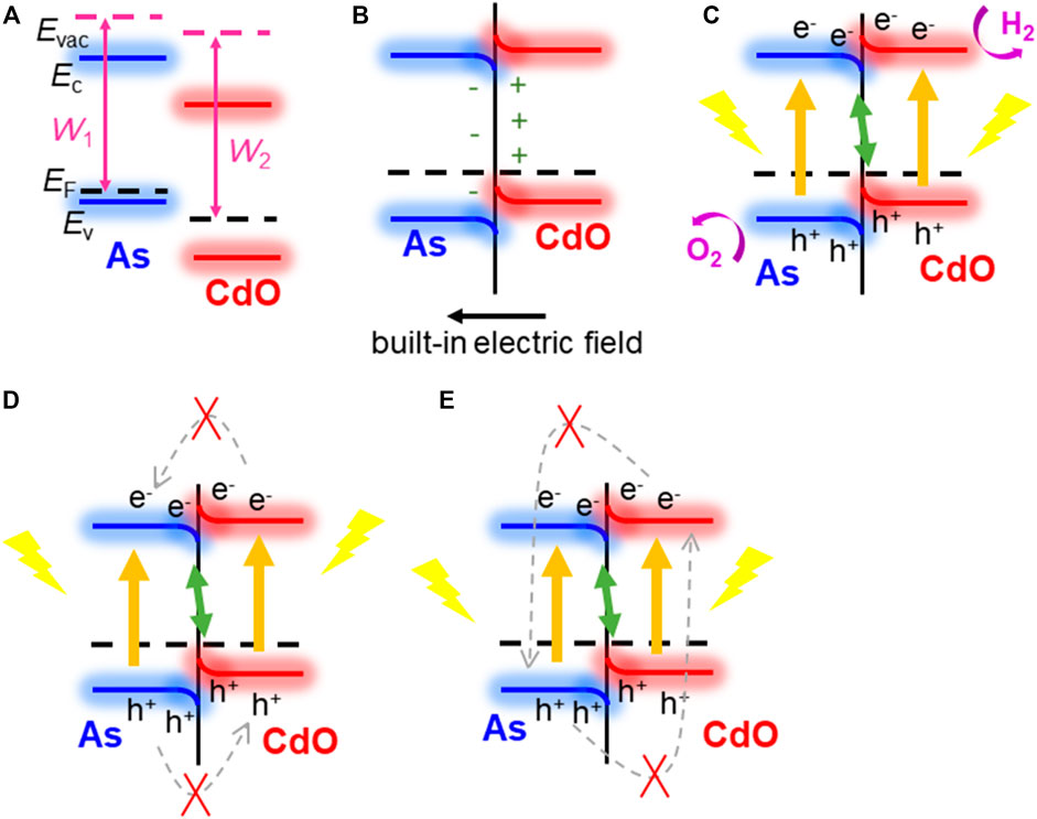
FIGURE 3. (A) The projected band structure and (B) the band-resolved charge densities of the CdO/As vdW heterostructure; the Fermi level is zero energy indicated by gray dashed line. (C) Schematic of the migration for the CdO/As vdW heterostructure using as a photocatalyst.
Next, we explain how the direct Z-scheme structure can be used as a photocatalyst in CdO/As vdW heterostructure. It is of great significance to calculate the work function (W) difference between single-layer CdO and single-layer As, which is a prerequisite for driving charge redistribution and forming built-in electric field through CdO/As vdW heterostructure interface (Bai et al., 2015; Liu et al., 2016). Shown in Figure 4A, Before the intercourse of single-layer CdO and single-layer As, the work functions of CdO (W2) and As (W1) are calculated to be 5.783 and 5.443 eV respectively. It can be seen from the calculation results that W1 is less than W2. According to the electron transfer mechanism, it can be concluded that electrons will be transferred from CdO layer to As layer until the Fermi level conforms to the equilibrium of Anderson rule (Zhang and Yates, 2012), shown in Figure 4B. Due to the transfer of electrons from CdO layer to As layer, positive holes are left in CdO layer, while negative electrons are accumulated in As layer, and a built-in electric field is generated at the interface. Subsequently, the electrons in the CdO layer and the negative charges in the As layer repel each other, which leads to the upward bending of the CdO band and the downward bending of the As layer at the interface for the same reason (Zhang and Yates, 2012; Huang et al., 2017). After photon excitation, both CdO and As can induce electrons and holes, as shown in Figure 4C. In this case of band bending, it is best to use the direct Z-scheme to transform the structure (Xu et al., 2018). The bending mode and built-in electric field of the band support the recomposite of light photogenerated holes in the VB of the CdO and photogenerated electrons in the CB of the As. Furthermore, this built-in electric field and extra potential barrier, which is also generated by band bending, will obstacle the flowing of the photogenerated electrons from CB of the CdO to the As, and the photogenerated holes from VB of the As to CdO, shown as Figure 4D. The built-in electric field also has ability to prevent the recomposite of the photogenerated electron in the CB of the CdO to the holes in the VB of the As, explained as Figure 4E. Therefore, the CdO/As vdW heterostructure can be considered as a potential direct Z-type photocatalyst in water splitting.
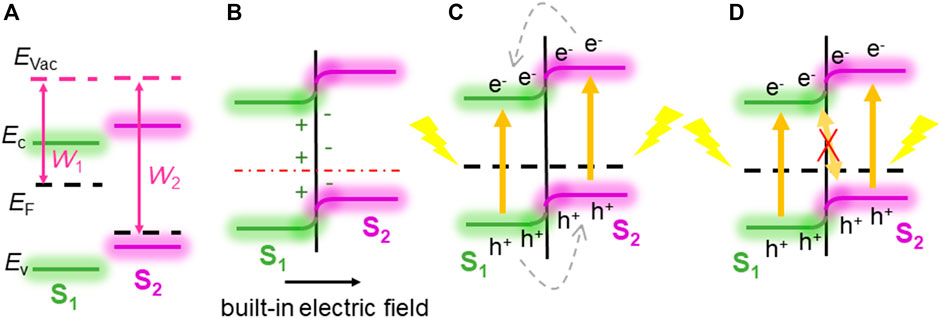
FIGURE 4. The direct Z-scheme mechanism demonstration for CdO/As vdW heterostructure: (A) before combining, (B) in combining; (C–E) photoinduced charge carrier migration process.
However, the process that the built-in electric field generated by the band bending trend inducing the photogenerated electrons and holes moving mode provides the Z-scheme photocatalytic mechanism for CdO/As vdW heterostructure to decompose the water is not coincidental. It is contributed form the critical band bending trend of the CdO/As vdW heterostructure. In contrast, another band bending method, such as p–n heterostructure, will not result the Z-scheme photocatalytic path for the photoinduced charges. As shown in Figure 5A, when the heterostructure is formed by n-type (work function of W1) and p-type semiconductors (work function of W2), the W1 is smaller than W2, free electrons can move from n-type material to p-type material, inducing the band of the n-type semiconductor bending upward, while the band of the p-type semiconductor bending downward across the interface of the heterostructure. Subsequently, the built-in electric field is constructed, as shown in Figure 5B. Under this built-in electric field assistances, the electrons at the CB of the p-type material will prefer moving to the CB of the n-type material, and the photogenerated holes at the VB of the n-type semiconductor will choose to migrate to the VB of the p-type semiconductor (Figure 5C). Moreover, even the band alignment of this heterostructure satisfy the band edge positions of the Z-scheme photocatalyst, the built-in electric field resulted by this band bending trend will not boost a combination for the photoinduced electrons at the CB of the n-type semiconductor and the photoinduced holes at the VB of the p-type semiconductor (Figure 5D) (Xu et al., 2018). Therefore, the direct Z-scheme mechanism is an intrinsic property of the CdO/As vdW heterostructure.
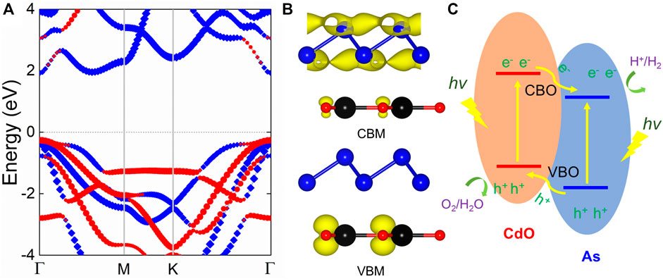
FIGURE 5. The p–n heterostructure schematic illustration: (A) before combining, (B) in combining, (C) transformation of photogenerated charge carriers in p–n heterostructure, and (D) suppressed transformation of photogenerated charge carrier in direct Z-scheme style.
As a potential candidate for direct Z-scheme photocatalyst to decompose water, the optical property is essential performance to be assessed. The optical absorption spectrum of the CdO, As and CdO/As vdW heterostructure are calculated in Figure 6A, which evidently explain the CdO/As vdW heterostructure can improve the visible light absorption capacity (wavelength range 380–800 nm). The obtained excellent absorption peak of the CdO/As vdW heterostructure is 8.47 × 104 cm−1 at the wavelength of 542 nm. Besides, enhancing solar energy conversion efficiency is the ultimate target for that, which demonstrates the indeed usage of solar energy for HER and OER (Lu et al., 2019). Therefore, we calculated STH efficiency (ηSTH) for the CdO/As vdW heterostructure. The obtained ηabs and ηcu are 58.1 and 20.1%, respectively. The ηSTH of the monolayered CdO, As and CdO/As vdW heterostructure is also calculated in the Table 2. The obtained ηSTH of the CdO/As vdW heterostructure as 11.67% indicates such Z-scheme photocatalyst possesses a novel STH efficiency, which is also higher than other reported photocatalysts, shown in Figure 6B. It worth noting that we assumed the 100% efficiency of the catalytic reaction for the calculations of the STH efficiency (Fu et al., 2018).
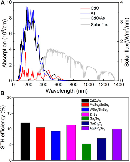
FIGURE 6. (A) The HSE06 method obtained optical absorption spectrum and (B) the STH efficiency of CdO/As vdW heterostructure comparing with other 2D materials (Fan et al., 2019; Jin et al., 2019; Yang et al., 2019).
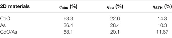
TABLE 2. The energy conversion efficiency of light absorption (ηabs), carrier utilization (ηcu) and STH (ηSTH) of the monolayered CdO, As and CdO/As vdW heterostructure.
Conclusions
Based on the first-principles calculation, firstly, we systematically studied the geometry and band structure of single-layer CdO and As. Then, the CdO/As heterostructure is constructed using vdW forces possessing a direct bandgap as 2.179 eV and a type-II band alignment structure is realized, which can limit the recomposite of photogenerated electron−hole pairs. Next, the band bending configuration of CdO/As vdW heterostructure is addressed, which demonstrates the potential Z-scheme conversion mechanism using as a photocatalyst for HER and OER. Furthermore, the excellent ηSTH of CdO/As vdW heterostructure is obtained by 11.67%. All our results show that the CdO/As vdW heterostructure can be used as a potential direct Z-scheme photocatalyst for water splitting.
Data Availability Statement
The raw data supporting the conclusion of this article will be made available by the authors, without undue reservation.
Author Contributions
Conceptualization, KR, JL, and RZ; methodology, KR; software, JY; validation, QS; formal analysis, KR and JL; investigation, RZ; resources, KR; data curation, KR; writing—original draft preparation, RZ; writing—review and editing, RZ; visualization, RZ; supervision, QS; project administration, QS; funding acquisition, KR.
Conflict of Interest
The authors declare that the research was conducted in the absence of any commercial or financial relationships that could be construed as a potential conflict of interest.
Publisher’s Note
All claims expressed in this article are solely those of the authors and do not necessarily represent those of their affiliated organizations, or those of the publisher, the editors and the reviewers. Any product that may be evaluated in this article, or claim that may be made by its manufacturer, is not guaranteed or endorsed by the publisher.
Acknowledgments
This investigation thanks the Collaborative education project of industry university cooperation of the Ministry of Education (Grant number: 202002276033).
References
Ali, A., Zhang, J.-M., Shahid, I., Muhammad, I., Ahmad, I., and Kabir, F. (2021). Theoretical study on the electronic structure, optical and photocatalytic properties of type-II As/CdO van der Waals heterostructure. Physica E: Low-dimensional Syst. Nanostructures 134, 114888. doi:10.1016/j.physe.2021.114888
Bai, S., Jiang, J., Zhang, Q., and Xiong, Y. (2015). Steering Charge Kinetics in Photocatalysis: Intersection of Materials Syntheses, Characterization Techniques and Theoretical Simulations. Chem. Soc. Rev. 44, 2893–2939. doi:10.1039/c5cs00064e
Cai, Y., Zhang, G., and Zhang, Y.-W. (2014). Polarity-Reversed Robust Carrier Mobility in Monolayer MoS2 Nanoribbons. J. Am. Chem. Soc. 136, 6269–6275. doi:10.1021/ja4109787
Capelle, K. (2006). A Bird's-Eye View of Density-Functional Theory. Braz. J. Phys. 36, 1318–1343. doi:10.1590/s0103-97332006000700035
Chaurasiya, R., and Dixit, A. (2019). Point Defects Induced Magnetism in CdO Monolayer: A Theoretical Study. J. Magnetism Magn. Mater. 469, 279–288. doi:10.1016/j.jmmm.2018.08.076
Chaurasiya, R., Raman, R., Tyagi, S., and Dixit, A. (2019). Strain Modulated Optoelectronic Properties of CdO Monolayer. J. Elec Materi 48, 3963–3969. doi:10.1007/s11664-019-07160-3
Chen, X., Tian, F., Persson, C., Duan, W., and Chen, N.-x. (2013). Interlayer Interactions in Graphites. Sci. Rep. 3, 3046. doi:10.1038/srep03046
Cui, Z., Luo, Y., Yu, J., and Xu, Y. (2021). Tuning the Electronic Properties of MoSi2N4 by Molecular Doping: A First Principles Investigation. Physica E: Low-dimensional Syst. Nanostructures 134, 114873. doi:10.1016/j.physe.2021.114873
Dai, C., Yin, Z., Wang, P., Miao, Q., and Chen, J. (2021). Analysis on Ground Surface in Ultrasonic Face Grinding of Silicon Carbide (SiC) Ceramic with Minor Vibration Amplitude. Ceramics International 47, 21959–21968. doi:10.1016/j.ceramint.2021.04.214
Ding, Z., Pei, Q.-X., Jiang, J.-W., Huang, W., and Zhang, Y.-W. (2016). Interfacial thermal Conductance in graphene/MoS2 Heterostructures. Carbon 96, 888–896. doi:10.1016/j.carbon.2015.10.046
Fan, Y., Wang, J., and Zhao, M. (2019). Spontaneous Full Photocatalytic Water Splitting on 2D MoSe2/SnSe2 and WSe2/SnSe2 vdW Heterostructures. Nanoscale 11, 14836–14843. doi:10.1039/c9nr03469b
Fu, C.-F., Sun, J., Luo, Q., Li, X., Hu, W., and Yang, J. (2018). Intrinsic Electric Fields in Two-Dimensional Materials Boost the Solar-To-Hydrogen Efficiency for Photocatalytic Water Splitting. Nano Lett. 18, 6312–6317. doi:10.1021/acs.nanolett.8b02561
Fujishima, A., and Honda, K. (1972). Electrochemical Photolysis of Water at a Semiconductor Electrode. Nature 238, 37–38. doi:10.1038/238037a0
Geim, A. K., and Novoselov, K. S. (2007). The Rise of Graphene. Nat. Mater 6, 183–191. doi:10.1038/nmat1849
Grimme, S., Antony, J., Ehrlich, S., and Krieg, H. (2010). A Consistent and Accurate Ab Initio Parametrization of Density Functional Dispersion Correction (DFT-D) for the 94 Elements H-Pu. J. Chem. Phys. 132, 154104. doi:10.1063/1.3382344
Grimme, S. (2006). Semiempirical GGA-type Density Functional Constructed with a Long-Range Dispersion Correction. J. Comput. Chem. 27, 1787–1799. doi:10.1002/jcc.20495
He, J., Ding, G., Zhong, C., Li, S., Li, D., and Zhang, G. (2018). Cr2TiC2-based Double MXenes: Novel 2D Bipolar Antiferromagnetic Semiconductor with Gate-Controllable Spin Orientation toward Antiferromagnetic Spintronics. Nanoscale 11, 356–364. doi:10.1039/c8nr07692h
He, J., Ding, G., Zhong, C., Li, S., Li, D., and Zhang, G. (2019). Remarkably Enhanced Ferromagnetism in a Super-exchange Governed Cr2Ge2Te6 Monolayer via Molecular Adsorption. J. Mater. Chem. C 7, 5084–5093. doi:10.1039/c8tc05530k
He, J., Hummer, K., and Franchini, C. (2014). Stacking Effects on the Electronic and Optical Properties of Bilayer Transition Metal Dichalcogenides MoS2, MoSe2, WS2, and WSe2. Phys. Rev. B 89, 075409. doi:10.1103/physrevb.89.075409
Heyd, J., Scuseria, G. E., and Ernzerhof, M. (2003). Hybrid Functionals Based on a Screened Coulomb Potential. J. Chem. Phys. 118, 8207–8215. doi:10.1063/1.1564060
Huang, Z.-F., Song, J., Wang, X., Pan, L., Li, K., Zhang, X., et al. (2017). Switching Charge Transfer of C3N4/W18O49 from Type-II to Z-Scheme by Interfacial Band Bending for Highly Efficient Photocatalytic Hydrogen Evolution. Nano Energy 40, 308–316. doi:10.1016/j.nanoen.2017.08.032
Jin, H., Zhang, H., Li, J., Wang, T., Wan, L., Guo, H., et al. (2019). Data-Driven Systematic Search of Promising Photocatalysts for Water Splitting under Visible Light. J. Phys. Chem. Lett. 10, 5211–5218. doi:10.1021/acs.jpclett.9b01977
Kamal, C., and Ezawa, M. (2015). Arsenene: Two-Dimensional Buckled and Puckered Honeycomb Arsenic Systems. Phys. Rev. B 91, 085423. doi:10.1103/physrevb.91.085423
Kresse, G., and Joubert, D. (1999). From Ultrasoft Pseudopotentials to the Projector Augmented-Wave Method. Phys. Rev. B 59, 1758–1775. doi:10.1103/physrevb.59.1758
Lee, T., Kim, S., and Jang, H. (2016). Black Phosphorus: Critical Review and Potential for Water Splitting Photocatalyst. Nanomaterials 6, 194. doi:10.3390/nano6110194
Li, Y., and Chen, X. (2014). Dirac Fermions in Blue-Phosphorus. 2d Mater. 1, 031002. doi:10.1088/2053-1583/1/3/031002
Liu, E., Chen, J., Ma, Y., Feng, J., Jia, J., Fan, J., et al. (2018). Fabrication of 2D SnS2/g-C3n4 Heterojunction with Enhanced H2 Evolution during Photocatalytic Water Splitting. J. Colloid Interf. Sci. 524, 313–324. doi:10.1016/j.jcis.2018.04.038
Liu, J., Cheng, B., and Yu, J. (2016). A New Understanding of the Photocatalytic Mechanism of the Direct Z-Scheme G-C3N4/TiO2 heterostructure. Phys. Chem. Chem. Phys. 18, 31175–31183. doi:10.1039/c6cp06147h
Liu, X., and Li, Z. (2015). Electric Field and Strain Effect on Graphene-MoS2 Hybrid Structure: Ab Initio Calculations. J. Phys. Chem. Lett. 6, 3269–3275. doi:10.1021/acs.jpclett.5b01233
Lou, J., Ren, K., Huang, Z., Huo, W., Zhu, Z., and Yu, J. (2021). Electronic and Optical Properties of Two-Dimensional Heterostructures Based on Janus XSSe (X = Mo, W) and Mg(OH)2: a First Principles Investigation. RSC Adv. 11, 29576–29584. doi:10.1039/d1ra05521f
Lu, B., Zheng, X., and Li, Z. (2019). Few-Layer P4O2: A Promising Photocatalyst for Water Splitting. ACS Appl. Mater. Inter. 11, 10163–10170. doi:10.1021/acsami.8b21001
Luo, Y., Ren, C., Xu, Y., Yu, J., Wang, S., and Sun, M. (2021). A First Principles Investigation on the Structural, Mechanical, Electronic, and Catalytic Properties of Biphenylene. Sci. Rep. 11, 19008. doi:10.1038/s41598-021-98261-9
Luo, Y., Ren, K., Wang, S., Chou, J.-P., Yu, J., Sun, Z., et al. (2019). First-Principles Study on Transition-Metal Dichalcogenide/BSe van der Waals Heterostructures: A Promising Water-Splitting Photocatalyst. J. Phys. Chem. C 123, 22742–22751. doi:10.1021/acs.jpcc.9b05581
Maeda, K., and Domen, K. (2007). New Non-oxide Photocatalysts Designed for Overall Water Splitting under Visible Light. J. Phys. Chem. C 111, 7851–7861. doi:10.1021/jp070911w
Meng, A., Zhu, B., Zhong, B., Zhang, L., and Cheng, B. (2017). Direct Z-Scheme TiO2/CdS Hierarchical Photocatalyst for Enhanced Photocatalytic H2-Production Activity. Appl. Surf. Sci. 422, 518–527. doi:10.1016/j.apsusc.2017.06.028
Miró, P., Audiffred, M., and Heine, T. (2014). An Atlas of Two-Dimensional Materials. Chem. Soc. Rev. 43, 6537–6554. doi:10.1039/c4cs00102h
Perdew, J. P., Burke, K., and Ernzerhof, M. (1996). Generalized Gradient Approximation Made Simple. Phys. Rev. Lett. 77, 3865–3868. doi:10.1103/physrevlett.77.3865
Qi, K., Xing, X., Zada, A., Li, M., Wang, Q., Liu, S.-y., et al. (2020). Transition Metal Doped ZnO Nanoparticles with Enhanced Photocatalytic and Antibacterial Performances: Experimental and DFT Studies. Ceramics Int. 46, 1494–1502. doi:10.1016/j.ceramint.2019.09.116
Ren, K., Sun, M., Luo, Y., Wang, S., Yu, J., and Tang, W. (2019). First-principle Study of Electronic and Optical Properties of Two-Dimensional Materials-Based Heterostructures Based on Transition Metal Dichalcogenides and boron Phosphide. Appl. Surf. Sci. 476, 70–75. doi:10.1016/j.apsusc.2019.01.005
Ren, K., Tang, W., Sun, M., Cai, Y., Cheng, Y., and Zhang, G. (2020). A direct Z-scheme PtS2/arsenene van der Waals heterostructure with high photocatalytic water splitting efficiency. Nanoscale 12, 17281–17289. doi:10.1039/d0nr02286a
Ren, K., Wang, K., Cheng, Y., Tang, W., and Zhang, G. (2020). Two-dimensional Heterostructures for Photocatalytic Water Splitting: a Review of Recent Progress. Nano Futures 4, 032006. doi:10.1088/2399-1984/abacab
Ren, K., Wang, S., Luo, Y., Chou, J.-P., Yu, J., Tang, W., et al. (2020). High-efficiency photocatalyst for water splitting: a Janus MoSSe/XN (X = Ga, Al) van der Waals heterostructure. J. Phys. D: Appl. Phys. 53, 185504. doi:10.1088/1361-6463/ab71ad
Ren, K., Yu, J., and Tang, W. (2019). A two-dimensional vertical van der Waals heterostructure based on g-GaN and Mg(OH)2 used as a promising photocatalyst for water splitting: A first-principles calculation. J. Appl. Phys. 126, 065701. doi:10.1063/1.5099125
Ren, K., Zheng, R., Xu, P., Cheng, D., Huo, W., Yu, J., et al. (2021). Electronic and Optical Properties of Atomic-Scale Heterostructure Based on MXene and MN (M = Al, Ga): A DFT Investigation. Nanomaterials 11, 2236. doi:10.3390/nano11092236
Sang, H. L., Parish, C. M., and Xu, J. (2012). Anisotropic Epitaxial ZnO/CdO Core/shell Heterostructure Nanorods. Nanoscale. Res. Lett. 7, 626.
Singh, A. K., Mathew, K., Zhuang, H. L., and Hennig, R. G. (2015). Computational Screening of 2D Materials for Photocatalysis. J. Phys. Chem. Lett. 6, 1087–1098. doi:10.1021/jz502646d
Subramanyam, T. K., Uthanna, S., and Srinivasulu Naidu, B. (1998). Preparation and Characterization of CdO Films Deposited by Dc Magnetron Reactive Sputtering. Mater. Lett. 35, 214–220. doi:10.1016/s0167-577x(97)00246-2
Sun, M., Chou, J.-P., Hu, A., and Schwingenschlögl, U. (2019). Point Defects in Blue Phosphorene. Chem. Mater. 31, 8129–8135. doi:10.1021/acs.chemmater.9b02871
Sun, M., Luo, Y., Yan, Y., and Schwingenschlögl, U. (2021). Ultrahigh Carrier Mobility in the Two-Dimensional Semiconductors B8Si4, B8Ge4, and B8Sn4. Chem. Mater. 33, 6475–6483. doi:10.1021/acs.chemmater.1c01824
Sun, M., and Schwingenschlögl, U. (2020). B2P6: A Two-Dimensional Anisotropic Janus Material with Potential in Photocatalytic Water Splitting and Metal-Ion Batteries. Chem. Mater. 32, 4795–4800. doi:10.1021/acs.chemmater.0c01536
Sun, M., and Schwingenschlögl, U. (2021). Structure Prototype Outperforming MXenes in Stability and Performance in Metal‐Ion Batteries: A High Throughput Study. Adv. Energ. Mater. 11, 2003633. doi:10.1002/aenm.202003633
Sun, M., and Schwingenschlögl, U. (2021). Unique Omnidirectional Negative Poisson's Ratio in δ-Phase Carbon Monochalcogenides. J. Phys. Chem. C 125, 4133–4138. doi:10.1021/acs.jpcc.0c11555
Sun, M., and Schwingenschlögl, U. (2020). δ-CS: A Direct-Band-Gap Semiconductor Combining Auxeticity, Ferroelasticity, and Potential for High-Efficiency Solar Cells. Phys. Rev. Appl. 14, 044015. doi:10.1103/physrevapplied.14.044015
Togo, A., Oba, F., and Tanaka, I. (2008). First-principles Calculations of the Ferroelastic Transition between Rutile-type and CaCl2-type SiO2 at High Pressures. Phys. Rev. B 78, 134106. doi:10.1103/physrevb.78.134106
Togo, A., and Tanaka, I. (2015). First Principles Phonon Calculations in Materials Science. Scripta Materialia 108, 1–5. doi:10.1016/j.scriptamat.2015.07.021
Vahedi Fakhrabad, D., Shahtahmasebi, N., and Ashhadi, M. (2015). Optical Excitations and Quasiparticle Energies in the AlN Monolayer Honeycomb Structure. Superlattices and Microstructures 79, 38–44. doi:10.1016/j.spmi.2014.12.012
Wang, B.-J., Li, X.-H., Cai, X.-L., Yu, W.-Y., Zhang, L.-W., Zhao, R.-Q., et al. (2018). Blue Phosphorus/Mg(OH)2 van der Waals Heterostructures as Promising Visible-Light Photocatalysts for Water Splitting. J. Phys. Chem. C 122, 7075–7080. doi:10.1021/acs.jpcc.7b12408
Wang, B., Wang, X., Wang, P., Yang, T., Yuan, H., Wang, G., et al. (2019). Bilayer MoSe2/HfS2 Nanocomposite as a Potential Visible-Light-Driven Z-Scheme Photocatalyst. Nanomaterials 9, 1706. doi:10.3390/nano9121706
Wang, B., Wang, X., Yuan, H., Zhou, T., Chang, J., and Chen, H. (2020). Direct Z-Scheme Photocatalytic Overall Water Splitting on Two Dimensional MoSe2/SnS2 Heterojunction. Int. J. Hydrogen Energ. 45, 2785–2793. doi:10.1016/j.ijhydene.2019.11.178
Wang, G., Gong, L., Li, Z., Wang, B., Zhang, W., Yuan, B., et al. (2020). A Two-Dimensional CdO/CdS Heterostructure Used for Visible Light Photocatalysis. Phys. Chem. Chem. Phys. 22, 9587–9592. doi:10.1039/d0cp00876a
Wang, G., Zhang, L., Li, Y., Zhao, W., Kuang, A., Li, Y., et al. (2020). Biaxial Strain Tunable Photocatalytic Properties of 2D ZnO/GeC Heterostructure. J. Phys. D: Appl. Phys. 53, 015104. doi:10.1088/1361-6463/ab440e
Xu, G., Yuan, J., Tao, X., Ding, B., Dou, H., Yan, X., et al. (2015). Absorption Mechanism of Carbon-Nanotube Paper-Titanium Dioxide as a Multifunctional Barrier Material for Lithium-Sulfur Batteries. Nano Res. 8, 3066–3074. doi:10.1007/s12274-015-0812-0
Xu, Q., Zhang, L., Yu, J., Wageh, S., Al-Ghamdi, A. A., and Jaroniec, M. (2018). Direct Z-Scheme Photocatalysts: Principles, Synthesis, and Applications. Mater. Today 21, 1042–1063. doi:10.1016/j.mattod.2018.04.008
Xu, Z., Li, Y., Li, C., and Liu, Z. (2016). Tunable Electronic and Optical Behaviors of Two-Dimensional Germanium Carbide. Appl. Surf. Sci. 367, 19–25. doi:10.1016/j.apsusc.2016.01.136
Yang, H., Ma, Y., Zhang, S., Jin, H., Huang, B., and Dai, Y. (2019). GeSe@SnS: Stacked Janus Structures for Overall Water Splitting. J. Mater. Chem. A. 7, 12060–12067. doi:10.1039/c9ta02716e
Yang, Q., Tan, C.-J., Meng, R.-S., Jiang, J.-K., Liang, Q.-H., Sun, X., et al. (2017). AlN/BP Heterostructure Photocatalyst for Water Splitting. IEEE Electron. Device Lett. 38, 145–148. doi:10.1109/led.2016.2633487
Yong, X., Zhang, J., and Ma, X. (2020). Effects of Intrinsic Defects on the Photocatalytic Water-Splitting Activities of PtSe2. Int. J. Hydrogen Energ. 45, 8549–8557. doi:10.1016/j.ijhydene.2020.01.066
Yuan, J., Cai, Y., Shen, L., Xiao, Y., Ren, J.-C., Wang, A., et al. (2018). One-dimensional Thermoelectrics Induced by Rashba Spin-Orbit Coupling in Two-Dimensional BiSb Monolayer. Nano Energy 52, 163–170. doi:10.1016/j.nanoen.2018.07.041
Yuan, J., Yang, Y., Cai, Y., Wu, Y., Chen, Y., Yan, X., et al. (2020). Intrinsic Skyrmions in Monolayer Janus Magnets. Phys. Rev. B 101, 094420. doi:10.1103/physrevb.101.094420
Yuan, L., Han, C., Yang, M.-Q., and Xu, Y.-J. (2016). Photocatalytic Water Splitting for Solar Hydrogen Generation: Fundamentals and Recent Advancements. Int. Rev. Phys. Chem. 35, 1–36. doi:10.1080/0144235x.2015.1127027
Zhang, L., and Singh, D. J. (2009). Electronic Structure and Thermoelectric Properties of Layered PbSe-WSe2 Materials. Phys. Rev. B 80, 075117. doi:10.1103/physrevb.80.075117
Zhang, Z., and Yates, J. T. (2012). Band Bending in Semiconductors: Chemical and Physical Consequences at Surfaces and Interfaces. Chem. Rev. 112, 5520–5551. doi:10.1021/cr3000626
Zhao, H., Li, E., Liu, C., Shen, Y., Shen, P., Cui, Z., et al. (2021). DFT computation of two-dimensional CdO/GaS van der Waals heterostructure: Tunable absorption spectra for water splitting application. Vacuum 192, 110434. doi:10.1016/j.vacuum.2021.110434
Zhong, C., Chen, Y., Xie, Y., Sun, Y.-Y., and Zhang, S. (2017). Semi-Dirac Semimetal in Silicene Oxide. Phys. Chem. Chem. Phys. 19, 3820–3825. doi:10.1039/c6cp08439g
Zhong, C., Wu, W., He, J., Ding, G., Liu, Y., Li, D., et al. (2019). Two-dimensional Honeycomb Borophene Oxide: strong Anisotropy and Nodal Loop Transformation. Nanoscale 11, 2468–2475. doi:10.1039/c8nr08729f
Zhong, C., Zhang, W., Ding, G., and He, J. (2019). Three-dimensional Graphene Networks Modified with Acetylenic Linkages for High-Performance Optoelectronics and Li-Ion Battery Anode Material. Carbon 154, 478–484. doi:10.1016/j.carbon.2019.08.030
Zhu, Z., Ren, K., Shu, H., Cui, Z., Huang, Z., Yu, J., et al. (2021). First-Principles Study of Electronic and Optical Properties of Two-Dimensional WSSe/BSe van der Waals Heterostructure with High Solar-to-Hydrogen Efficiency. Catalysts 11, 991. doi:10.3390/catal11080991
Keywords: two-dimensional, heterostructure, first-principles calculation, Z-scheme, photocatalyst
Citation: Ren K, Zheng R, Yu J, Sun Q and Li J (2021) Band Bending Mechanism in CdO/Arsenene Heterostructure: A Potential Direct Z-scheme Photocatalyst. Front. Chem. 9:788813. doi: 10.3389/fchem.2021.788813
Received: 03 October 2021; Accepted: 18 October 2021;
Published: 19 November 2021.
Edited by:
Guangzhao Wang, Yangtze Normal University, ChinaCopyright © 2021 Ren, Zheng, Yu, Sun and Li. This is an open-access article distributed under the terms of the Creative Commons Attribution License (CC BY). The use, distribution or reproduction in other forums is permitted, provided the original author(s) and the copyright owner(s) are credited and that the original publication in this journal is cited, in accordance with accepted academic practice. No use, distribution or reproduction is permitted which does not comply with these terms.
*Correspondence: Kai Ren, kairen@njfu.edu.cn; Qingyun Sun, sunqingyun@njfu.edu.cn
†These authors have contributed equally to this work and share first authorship