Article

Small-Signal Analysis and Control of Soft-Switching Naturally Clamped Snubberless Current-Fed Half-Bridge DC/DC Converter

by
Koyelia Khatun
1,
Vakacharla Venkata Ratnam
1,
Akshay Kumar Rathore
1,* and
Beeramangalla Lakshminarasaiah Narasimharaju
2
1
Department of Electrical and Computer Engineering, Gina Cody School of Engineering and Computer Science, SGW Campus, Concordia University, Montreal, QC H3G 1M8, Canada
2
Department of Electrical Engineering, National Institute of Technology, Warangal 506004, India
*
Author to whom correspondence should be addressed.
Submission received: 30 June 2020 / Revised: 19 August 2020 / Accepted: 25 August 2020 / Published: 3 September 2020

Abstract

:

Featured Application

Fuel cells and Battery Applications.

Abstract

This paper presents small-signal analysis of a soft-switching naturally clamped snubberless isolated current-fed half-bridge (CFHB) DC-DC converter using state-space averaging. A two-loop average current controller was designed and implemented on a digital signal processor. The complete design procedure is presented here. Simulation results using software PSIM 11.1 are shown to validate the stability of the control system and the controller design. Experimental results for the step changes in load current vividly demonstrated satisfactory transient performance of the converter and validated the developed small-signal model and the control design.

1. Introduction

Electric transportation, energy storage, renewable energy systems, hybrid electric vehicles (HEV), and fuel cell vehicles require bidirectional power electronics for power processing [1,2,3,4]. A DC-DC front-end converter is the major part of a fuel cell inverter, which boosts the low-voltage fuel cell stack’s voltage to the peak of utility line alternating current (AC) voltage [5]. Among various categories of high-frequency (HF) soft-switching isolated DC-DC converters, a current-fed converter is popular in fuel cell applications. Fuel cells produce low-voltage direct current (DC), which has a wide variation with load current and requires a high voltage conversion ratio [6,7,8,9,10]. Current-fed topologies offer high voltage gain with a stiff DC input current [11]. The historical problem with current-fed converters has been the necessity of a passive snubber [12,13] or an active-clamping circuit [14,15,16] to clamp voltage overshoot across the semiconductor devices at their turn-off. Passive snubbers lead to poor efficiency because the energy stored by the clamping capacitor is later dissipated into the resistor. However, better efficiency is obtained, along with zero voltage switching (ZVS) of the semiconductor devices, with an active-clamping circuit [14,15,16], at the cost of additional footprints of floating active device(s) and a large HF clamp capacitor for accurate and effective voltage clamping. Additionally, the boost factor of the converter is reduced as well as the high peak, and circulating currents can be observed at light load. In [17], a new modulation technique of high-voltage side devices was proposed to solve the voltage spike problem of primary devices, eliminating the requirement for an external snubber. A current-fed half-bridge DC-DC converter was proposed as shown in Figure 1 with a new modulation, which was studied in [17] to achieve zero current switching (ZCS) commutation of semiconductor devices along with natural device voltage clamping.
Steady-state analysis, power circuit design, and steady-state experimental performance results of the converter have previously been presented in [17]. However, its small-signal modeling, controller design, and dynamic performance results have not yet reported. The authors reported the small-signal modeling and derived the transfer functions in [18]. Controller design and simulation results were presented to show initial results and investigation on the transient performance of the converter. This paper presents systematic small-signal analysis and experimental results to demonstrate the closed-loop dynamic performance of the converter.

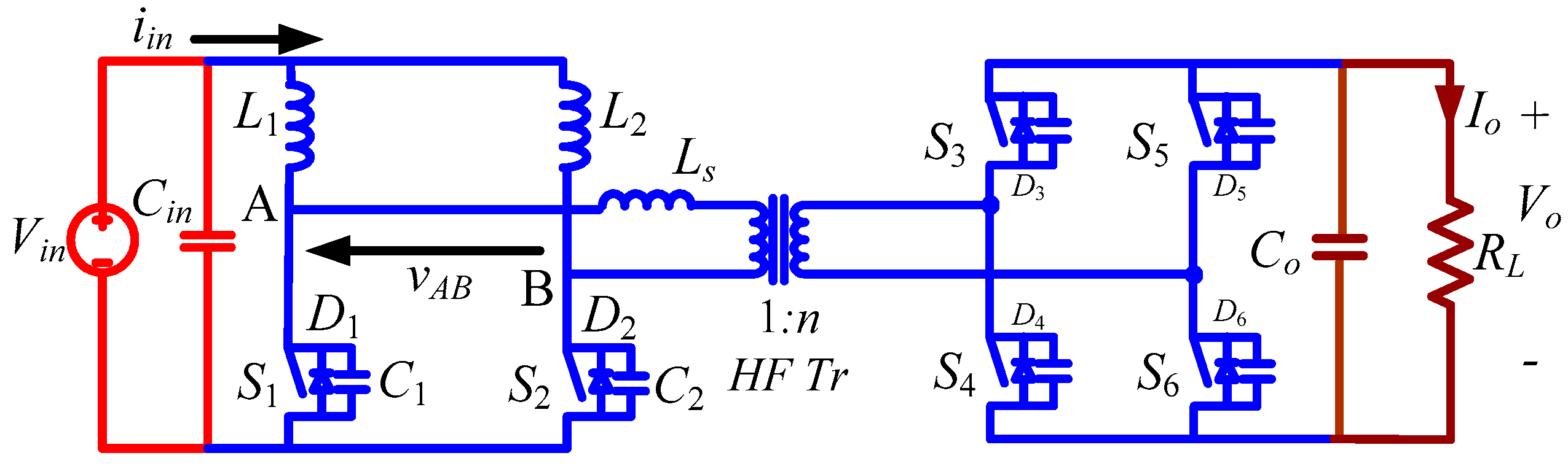
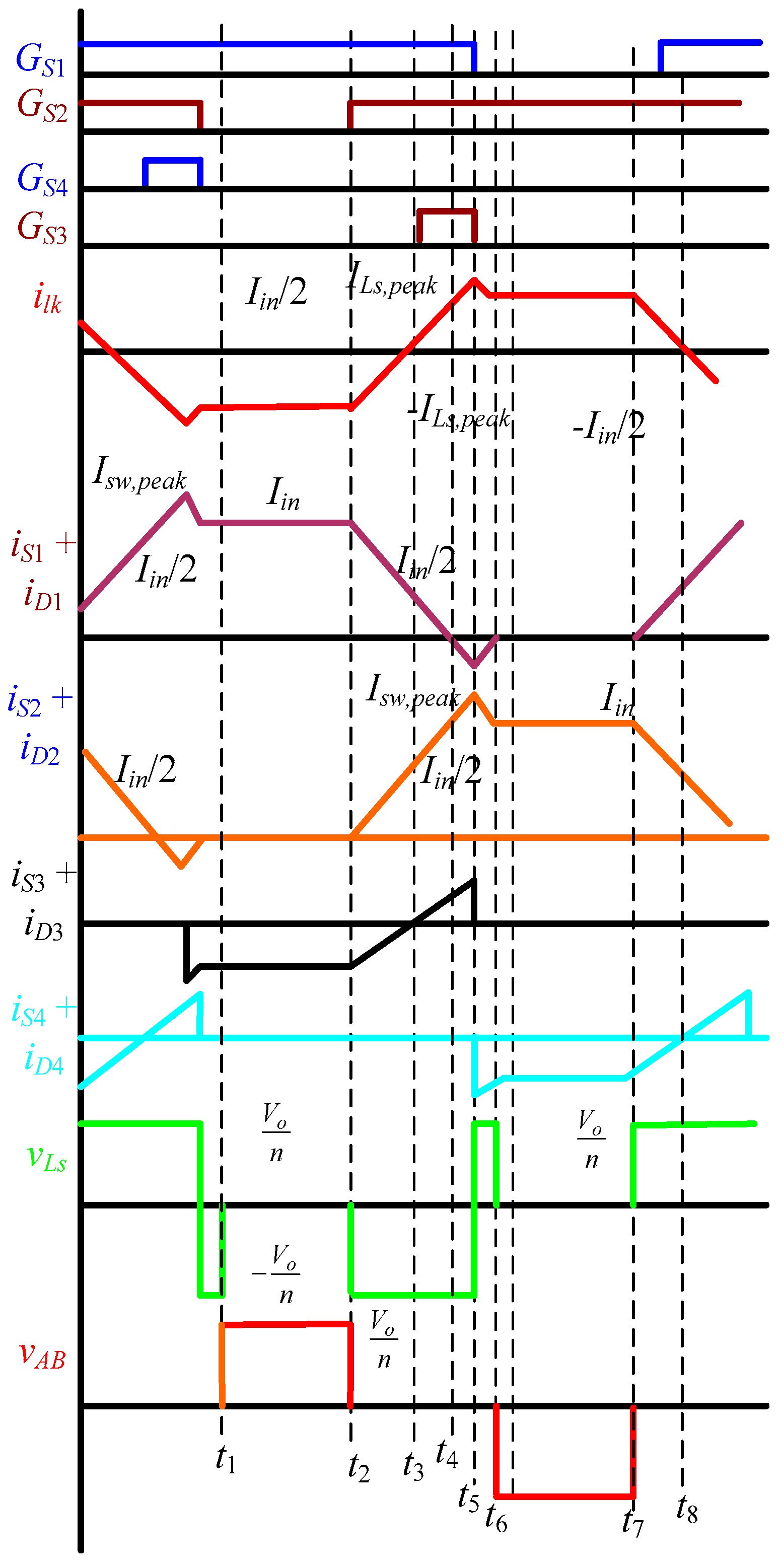
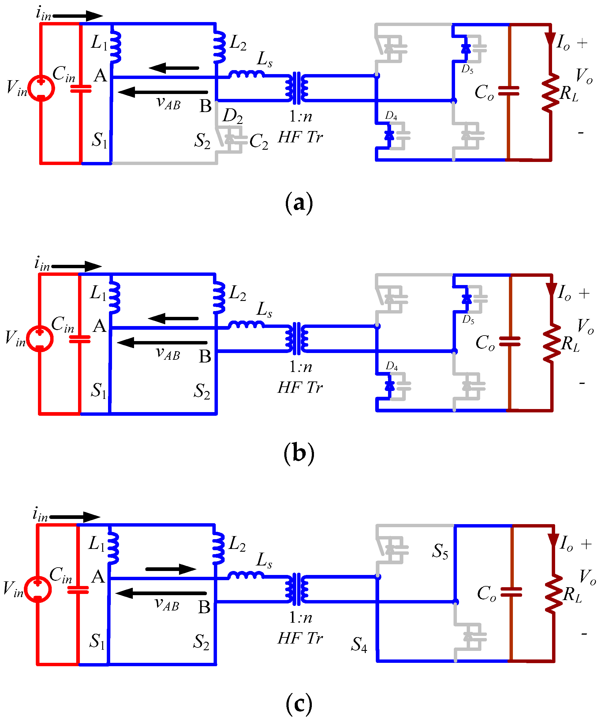
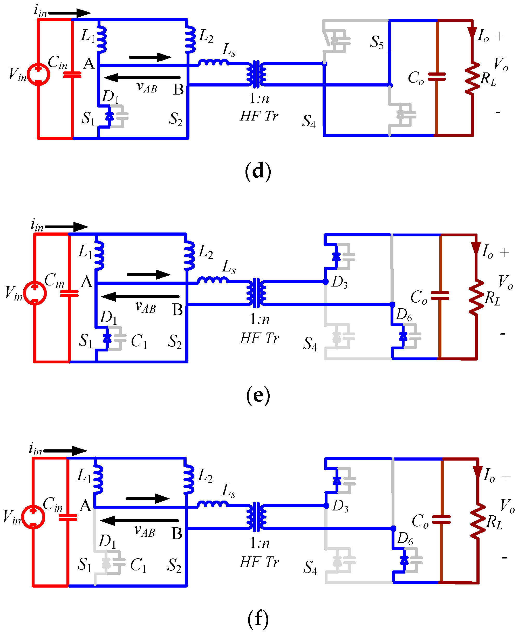
2. Small-Signal Analysis

The following procedure was followed to derive the small-signal model and converter transfer functions:
(1)
Make assumptions
(2)
Define state variables
(3)
Write state equations for each interval of operation
(4)
Average the state equations over a switching cycle
(5)
Introduce perturbation in state variables
(6)
Equate AC and DC quantities and proceed with AC equations
(7)
Take Laplace transform
(8)
Prepare matrix small-signal model
(9)
Calculate desired transfer functions
The following assumptions were made for the small-signal modeling of the converter: (1) all the power semiconductor devices are lossless and ideal; (2) inductors L1 and L2 are large enough to maintain constant current through them; (3) inductor Ls includes the leakage inductance of the HF transformer; steady-state operating waveforms are shown in Figure 2; (4) snubber/device capacitance charging and discharging intervals are short and neglected.
The primary side devices S1 and S2 are operated with identical gating signals phase-shifted with each other by 180°. The duty cycle of the primary switches is always kept above 50%. The operation during different intervals in a one-half switching cycle is explained with equivalent circuits shown in Figure 3.
State variables defined for the small-signal modeling of the converter are: (1) currents through the transformer leakage inductor ilk1 and ilk2; (2) input inductor current iin; (3) output voltage vo; (4) input voltage vin; (5) duty cycle loss d.
Interval 1 (Figure 3a; t1 < t < t2)
During this interval, primary side switch S1 and anti-parallel body diodes D4 and D5 of secondary switches are conducting to rectify the HF AC waveform across the transformer secondary. Power is transferred to the load through an HF transformer. Transformer primary current is negative and constant. Switch S1 is carrying the entire input current. State equations of this interval are:
L 1 d i L 1 d t = v i n    
C o d v o d t = i L s n v o R L
L s d i L s d t = 0
Interval 2 (Figure 3b; t2 < t < t3)
Primary side switch S2 is turned on and starts conducting. The current from S1 is transferred to the switch S2 through the transformer primary winding with a slope limited by transformer leakage inductance Ls. State equations of this interval are:
  L 2 d i L 2 d t = v i n
  L s d i L s d t = v o n
Interval 3 (Figure 3c; t3 < t < t4)
Secondary side devices S4 and S5 are turned on with ZVS. The current waveforms follow the same pattern and slope. State equations of interval 2 still hold good.
Interval 4 (Figure 3d; t4 < t < t5)
Primary side device S1 turns off with ZCS, and its anti-parallel body diode starts conducting. State equations of interval 2 still hold good.
Interval 5 (Figure 3e; t5 < t < t6)
Secondary side devices S4 and S5 are forced commutated, and anti-parallel body diodes D3 and D6 of secondary switches take over the current.
L s d i L s d t = V o n    
Equations (1), (3), and (5) hold good for inductor currents i L 1 ,   i L 2 , and output capacitor c o .
Identically, state equations for the other half-cycle can also be derived. State equations are averaged over an HF cycle. The average value for the rate of change of iLs over one complete HF cycle is zero, and the averaged state equation is:
L s d i L s d t =   0
So, the state variable iLs is omitted for the following analysis. Define: d1Ts = t2t1, d2Ts = t3t2, d3Ts = t4t3, d4Ts = t5t4, d5Ts = t6t5, d6Ts = t7t6, d7Ts = t8t7, d8Ts = = t9t8, d9Ts = t10t9, d10Ts = tst10.
The averaged state equations of defined state variables over an HF cycle are given:
L 1 d i L 1 d t =   v i n d 6 v o n
L 2 d i L 2 d t =   v i n d 1 v o n `
C o d v o d t =   i a v e r a g e v o R L
where iaverage is the average current feeding the output capacitor and load from secondary side H-bridge switches and is given by:
i a v e r a g e =   i L 2 n ( d 1 ) +   i L 1 n ( d 6 )
Substituting Equation (12) into Equation (11) gives:
C o d v o d t =   i L 2 n ( d 1 ) +   i L 1 n ( d 6 ) v o R L
The duty ratio of the main switches, including conduction of the anti-parallel diodes, is defined as:
d = dS1 = d1 + d2 + d3 + d4 + d5 + d7 + d8 + d9 + d10
d = dS2 = d2 + d3 + d4 + d5 + d6 + d7 + d8 + d9 + d10
Perturbation is introduced around the steady-state values of the state variables and input voltage such that i L 1 = I L + î L 1 , i L 2 = I L +   î L 2 , v i n = V i n + v ^ i n , v o = V o + v ^ o , d s 1 = D + d ^ s 1 , and d s 2 = D + d ^ s 2 . The state equations are modified to the following:
L 1 d ( I L 1 + î L 1 ) d t = ( V i n + v ^ i n ) ( 1 D d ^ s 1 ) ( V o + v ^ o ) n
L 2 d ( I L 2 + î L 2 ) d t = ( V i n +   v ^ i n )   ( 1 D d ^ s 2 ) ( V o +   v ^ o ) n
C o d ( V o + v ^ o ) d t = ( I L 1 + î L 1 n ) ( 1 D d ^ s 1 ) + ( I L 2 +   î L 2 n ) ( 1 D d ^ s 2 )   ( V o + v ^ o R L )
Neglecting the second order terms and steady-state or DC terms results in the following equations:
L 1 d î L 1 d t = v ^ i n   ( 1 D ) v ^ 0 n + d ^ s 1 V o n
L 2 d î L 2 d t = v ^ i n   ( 1 D ) v ^ o n +   d ^ s 2 V o n
C o d v ^ o d t = ( 1 D ) î L 1 n + ( 1 D ) î L 2 n I L 1 n d ^ s 1 I L 2 n d ^ s 2   v ^ o R L
Taking Laplace transform, and then solving results in:
s L 1 î L 1 ( s ) + ( 1 D ) v ^ o ( s ) n = V o n d ^ s 1 ( s ) +   v ^ i n ( s )
s L 2 î L 2 ( s ) + ( 1 D ) v ^ o ( s ) n = V o n d ^ s 2 ( s ) +   v ^ i n ( s )
( 1 D ) n î L 1 ( s ) + ( 1 D ) n   î L 2 ( s ) ( s C o + 1 R L ) v ^ o ( s ) = I L 1 n d ^ s 1 ( s ) + I L 2 n d ^ s 2 ( s )
Writing in matrix form:
[ î L 1 ( s ) î L 2 ( s ) v ^ o ( s ) ] =   [ A ( s ) ] ·   [ V o n 0 I L 1 n ] · d ^ s 1 ( s ) + [ A ( s ) ] ·   [ 0 V o n I L 2 n ] d ^ s 2 ( s ) + [ A ( s ) ] · [ 1 1 0 ] v ^ i n ( s )
where
A ( s ) = [ s L 1 0 ( 1 D ) n 0 s L 2 ( 1 D ) n ( 1 D ) n ( 1 D ) n ( s C o + 1 R L ) ] 1
s L ( î L 1 ( s ) + î L 2 ( s ) ) + 2 ( 1 D ) v ^ o ( s ) n = V o n ( d ^ s 1 ( s ) +   d ^ s 2 ( s ) ) + 2   v ^ i n ( s )
Writing in matrix form:
[ î L 1 ( s ) + î L 2 ( s ) v ^ o ( s ) ] =   [ A ( s ) ] ·   [ v o n I L n ] · ( d ^ s 1 ( s ) + d ^ s 2 ( s ) ) + [ A ( s ) ] · [ 2 0 ] v ^ i n ( s )
where
A ( s ) = [ s L 2 ( 1 D ) n ( 1 D ) n ( s C o + 1 R L ) ] 1
The control-to-output transfer function is obtained from Equation (28) by keeping v ^ i n = 0 , resulting in the following equation:
v ^ o ( s ) d ^ s 1 ( s ) + d ^ s 2 ( s ) = ( 1 D ) V o n 2 s L . I L n ( L C o ) s 2 + L R L s + 2 ( 1 D ) 2 n 2

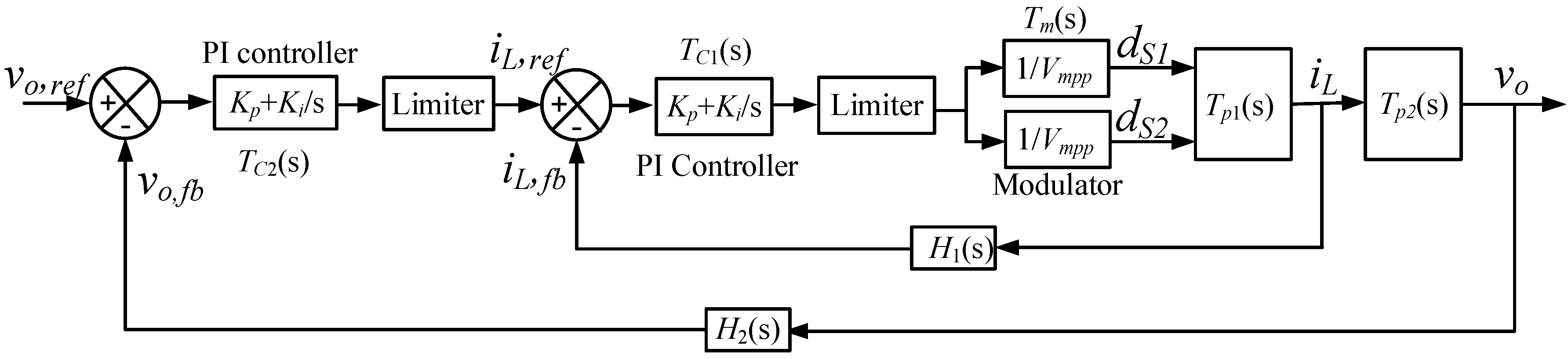
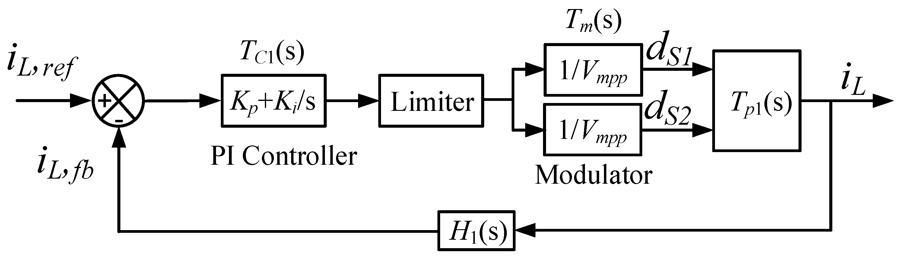
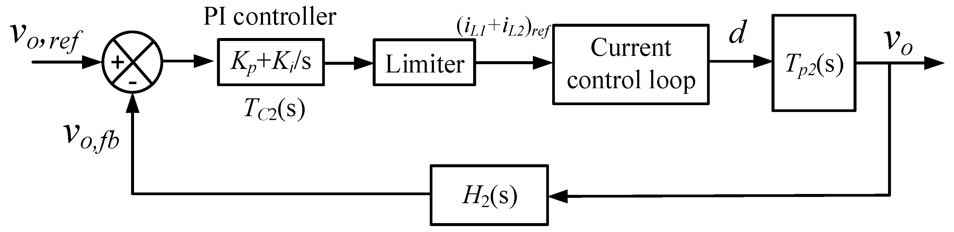
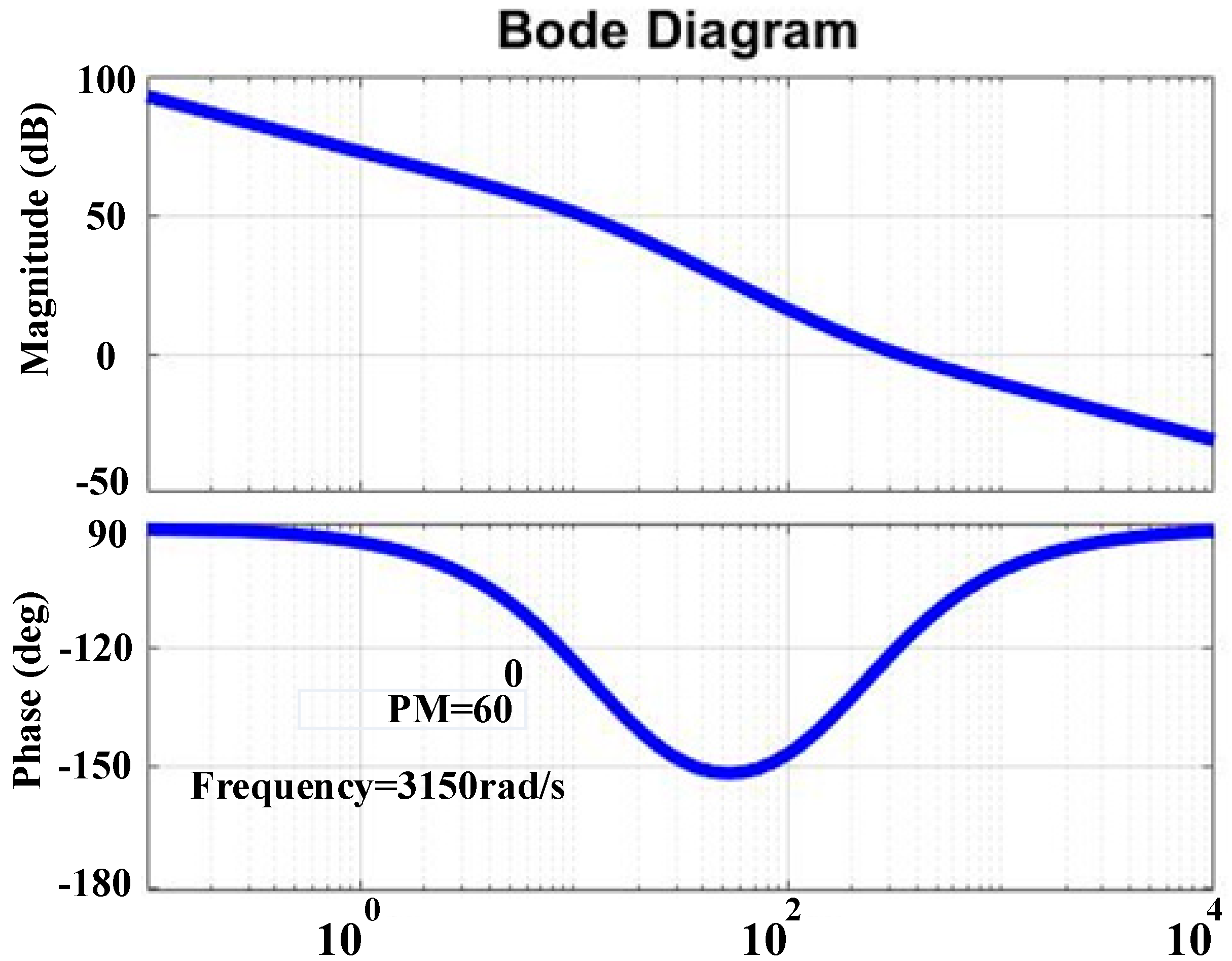
3. Two-Loop Closed-Loop Control Design

The two-loop control system is shown in Figure 4 with two proportional integral (PI) controllers and two identical modulators phase-shifted by 180°. Active current ripple is the major issue in the design of a fuel cell converter. The key to ripple reduction is to control the average inductor current iL to be DC, which requires separating the bandwidths of voltage and current loops far apart using a slow voltage loop and a fast current loop [19]. Bandwidth (BW) of the inner current loop is selected to be higher than the outer voltage loop, which simplifies the design [20]. Therefore, it is possible to adjust the inductor current more quickly than the load voltage. The outer voltage loop regulates the load voltage by deriving reference for the input inductor current, iL1,ref, and iL2,ref reference. Inductor currents iL1 and iL2 are tuned to this reference value by adjusting the duty ratio of the switches.
A bode plot of the control-to-output voltage transfer function given by Equation (30) is given in Figure 5. The phase margin (PM) is negative. This makes the system sensitive to small disturbances in operating points of input or source voltage and load current. Figure 6 shows that this transfer faction has right half plane zero, which adds a negative phase to the system. Instead of the phase increasing from 0 to 90 degrees, its phase increases from 0 to −90 degrees. This causes a delay in system response, which can lead to instability if not properly compensated.

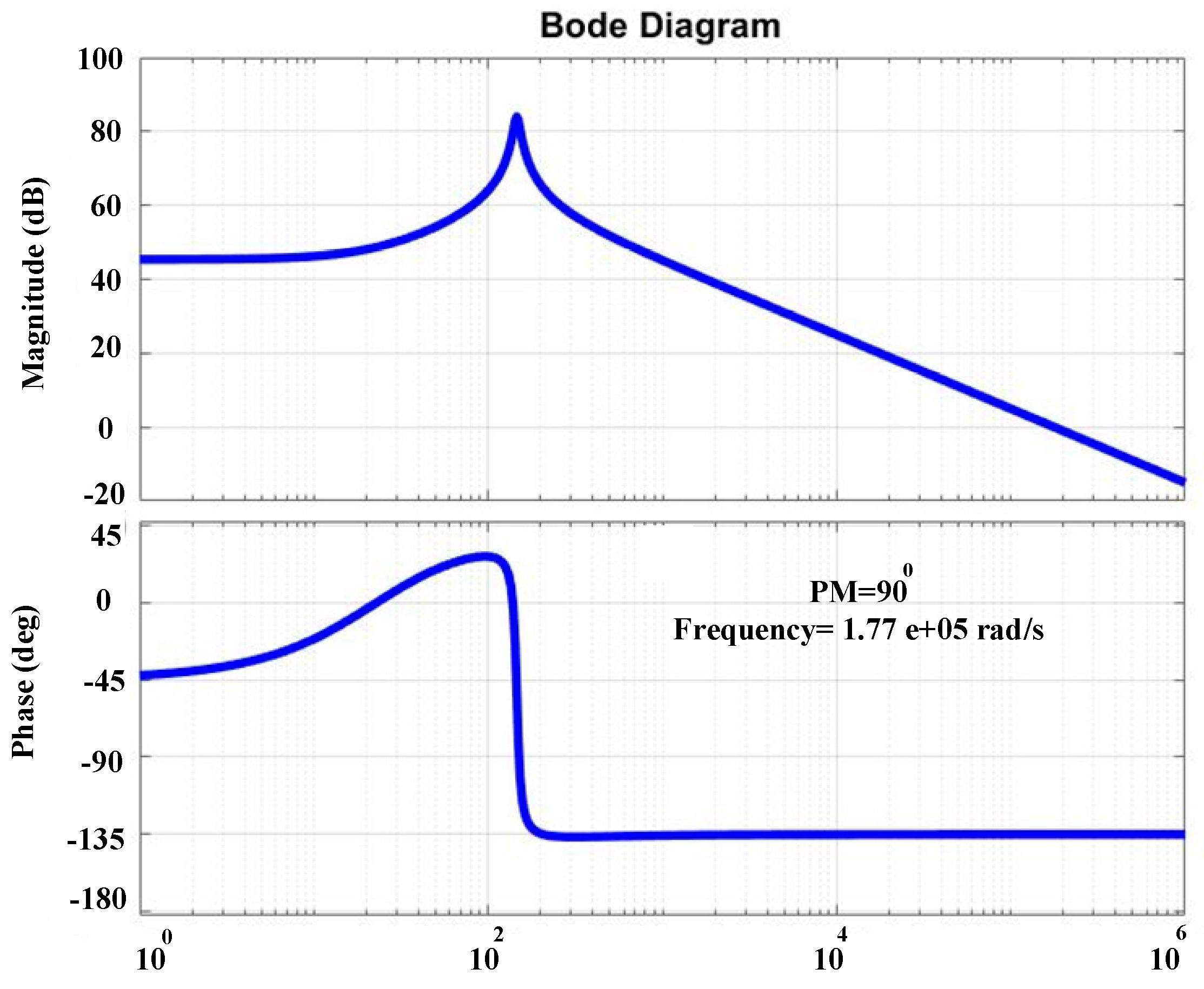
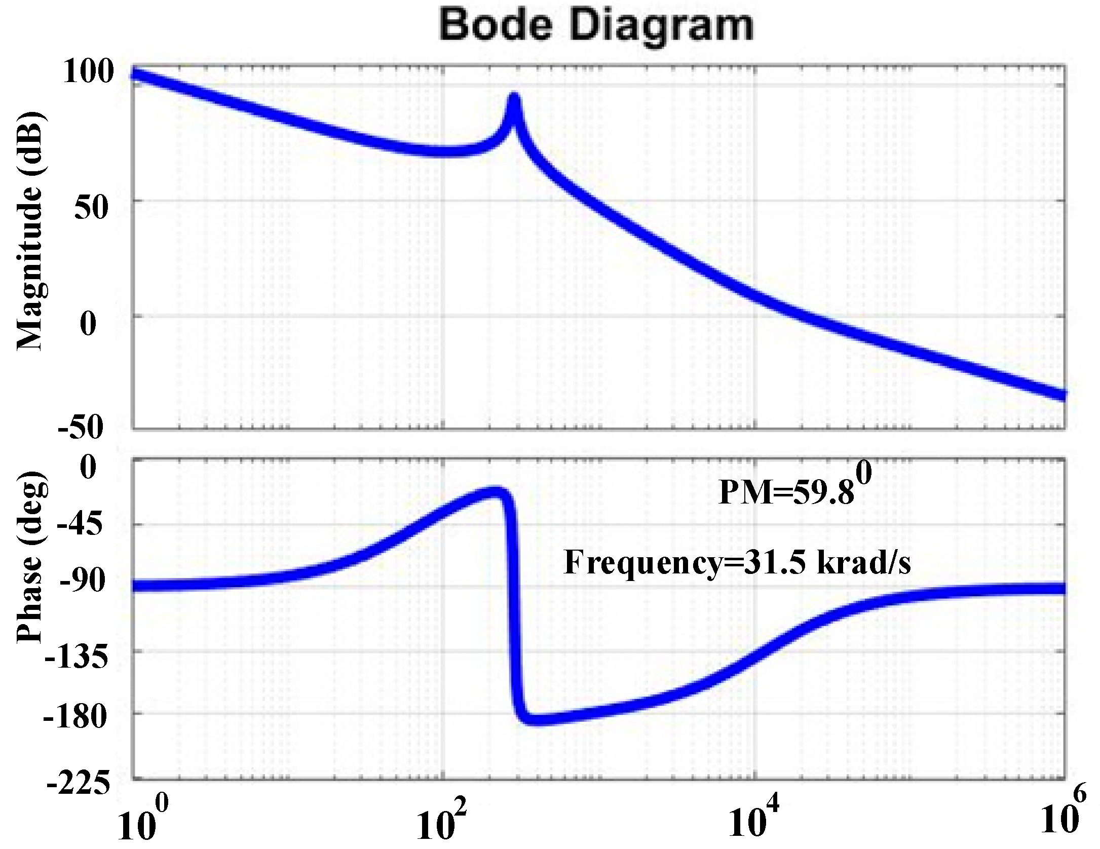
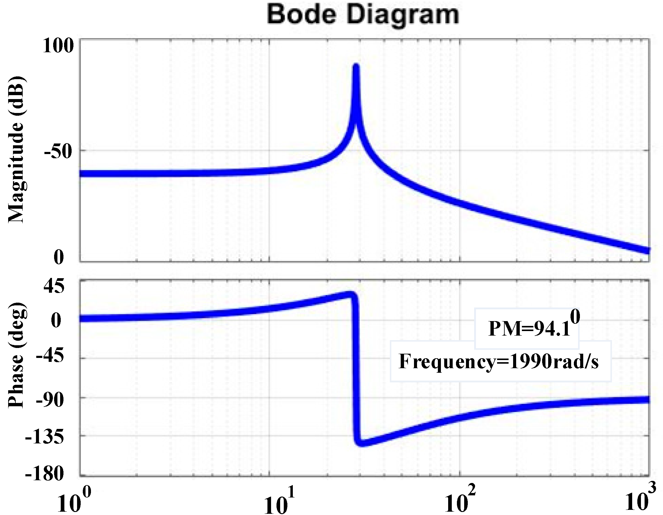
3.1. Current Control Loop Design

The schematic diagram of the inner current control loop is shown in Figure 7. The input inductor current is fed back to the error amplifier with the gain of H1(s). The error is processed by a PI controller, and the output of the controller is compared with the modulator to generate the gating signals of the devices. The inductors’ currents iL1 and iL2 are then regulated by adjusting the duty ratio of the switches.
Duty ratio to the inductor current transfer function is derived from Equation (27) and given by:
î L 1 ( s ) + î L 2 ( s ) d ^ s 1 ( s ) + d ^ s 2 ( s ) = ( C o V o n ) s + V o n R L + 2 ( 1 D ) n I L n ( L C o ) s 2 + L R L s + 2 ( 1 D ) 2 n 2
For the given specifications as shown in Table 1, the duty ratio to inductor current transfer function is given by:
T p 1 ( s ) = î L 1 ( s ) + î L 2 ( s ) d ^ s 1 ( s ) + d ^ s 2 ( s )     = 0.004542 s + 0.331514 4.26 × 10 8 s 2 +   5.847 × 10 7   s + 3.472 × 10 3    
The gain margin and PM of the current control loop without controller is plotted in Figure 8, which shows PM = 90 ° at 177 krad/s. The PI controller is designed at PM of 60 ° in Figure 9 to increase the low-frequency gain and to reduce the steady-state error [21].
The transfer function of a PI controller is given by:
T C 1 ( s ) = K p + K i s = K p ( s + K i / K p ) s
The open-loop transfer function of the current loop is given by:
T O L 1 ( s ) = T C 1 ( s ) × T m ( s ) × T p 1 ( s ) × H 1 ( s )
LEM sensor LA25-NP is used to sense the inductor current and to provide the isolation between power circuit and controller. Here, H1(s) is the current feedback gain and Tm(s) is the overall gain of the modulator.
Here, the current feedback gain is selected as H1(s) = 1.
Overall gain of the modulator is chosen to be:
T m ( s ) = 1 10
To realize PM = 60°, the following angle condition for the open-loop transfer function is applied:
T O L 1 ( j w c ) = P M 180 °
T O L I ( j w c ) = 106572 K p ( j w c + K i K p ) ( j w c + 73.02   ) j w c ( j w c 2 +   13.72 j w c + 81502.34 j w c )
To realize the desired crossover frequency, the following gain condition of unity is applied for the open-loop transfer function, i.e., | T O L 1 ( j w c ) | = 1 :
k p 2 ( 1.5625   × 10 10 +   k i k p 2 ) = 4.875   × 10 11
PI controller parameters are designed to obtain PM of 60° [21,22] at the gain crossover frequency of 31.5k rad/s (5000 Hz) (Figure 9). Low-frequency gain is improved. It results in the gain Kp and Ki as 0.16 and 7269.58 , respectively.

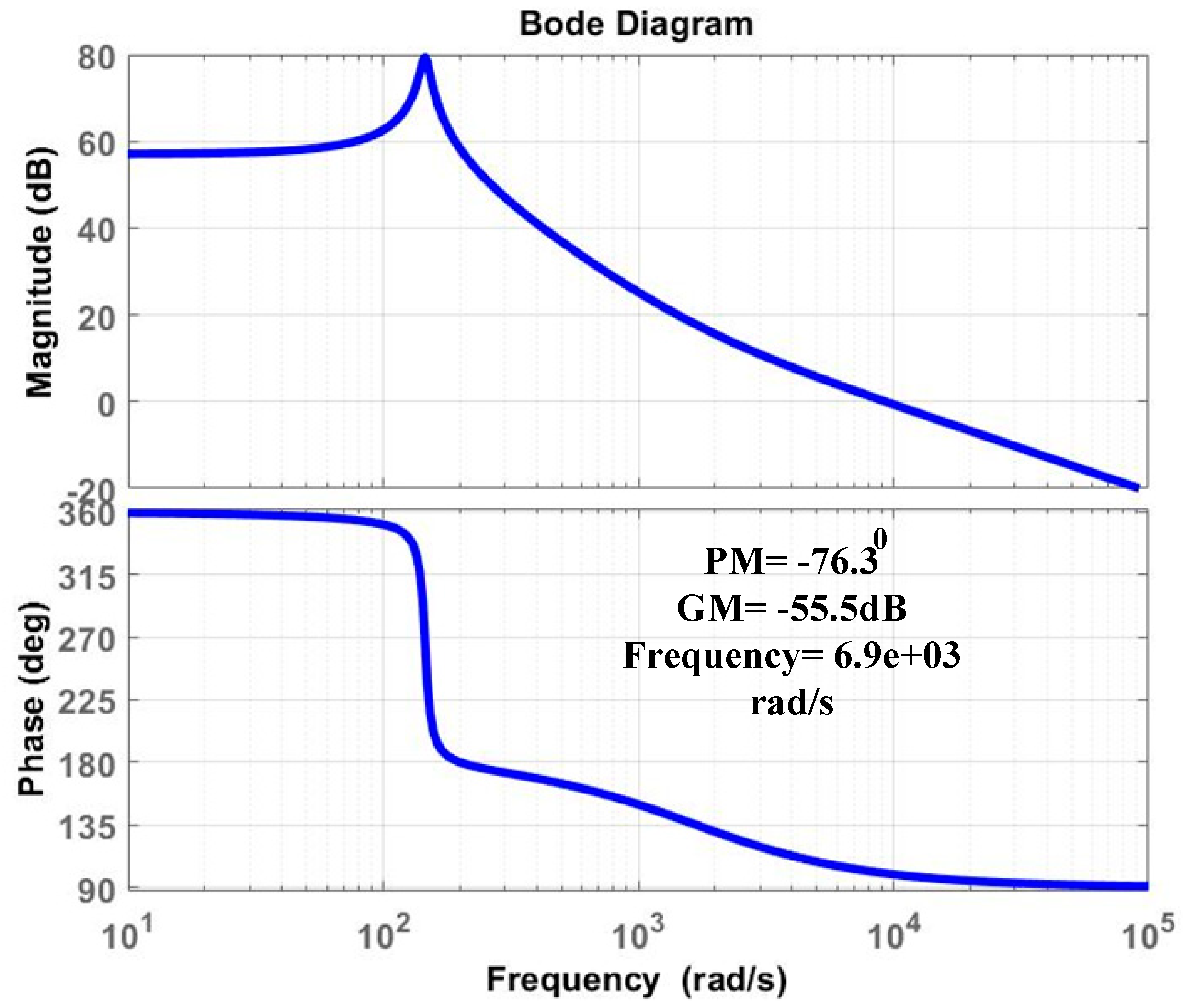
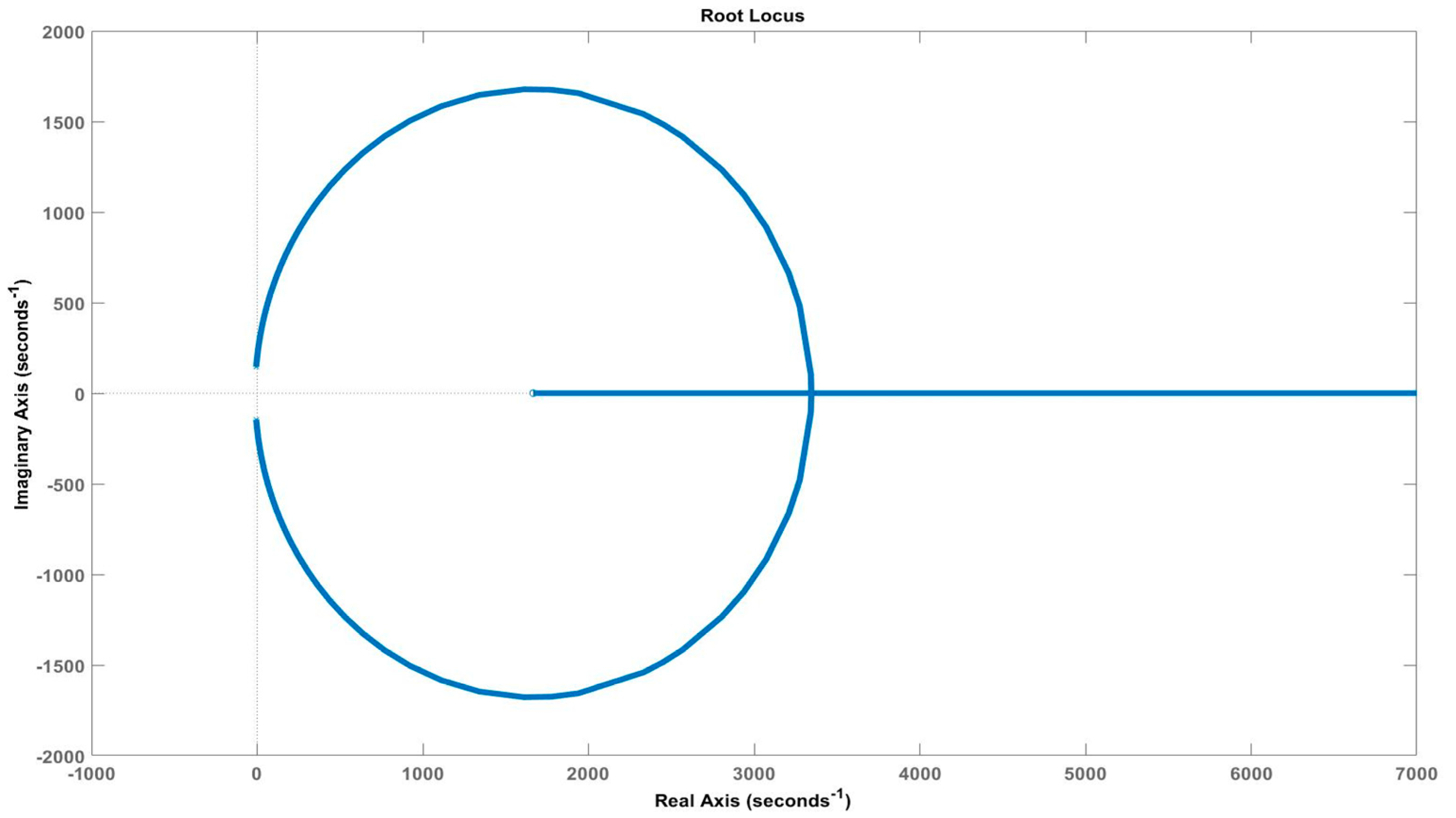
3.2. Voltage Control Loop Design

The outer voltage control loop regulates the output voltage at the reference value by setting reference for the current through the input inductors as shown in Figure 10. The inner current control loop has faster dynamics compared to the outer voltage loop. Hence, the current loop dynamics are neglected during the design of the voltage controller [23]. Its transfer function is not included, and the perturbation in the duty cycle can be neglected. Therefore, the inductor current to output voltage transfer function Tp2(s) is obtained as:
T p 2 ( s ) = v o ( s ) î L 1 ( s ) + î L 2 ( s ) = ( 1 D ) n C o ( s + 1 R L C o )
T P 2 ( s ) = 0.35 0.001848 s + 0.025
LEM sensor LV20-P is used to sense output voltage and also to provide the necessary isolation. Here, the voltage feedback gain is chosen as:
H 2 ( s ) = 24
The PI controller transfer function TC2(s) is given by Equation (33).
Figure 11 shows the bode plot for the uncompensated voltage control loop. For the given specifications and selected component values, the crossover frequency is high with poor low-frequency gain.
The overall open-loop transfer function of the voltage loop is given by:
T O L 2 ( s ) = T C 2 ( s ) × T p 2 ( s ) × H 2 ( s ) × 1 H 1 ( s ) ( 47 )
T O L I ( s ) = 0.35 K p ( s + K i K p ) 0.001848 s 2 + 0.025 s  
The gain crossover frequency for the voltage controller is selected to be 10 times slower than that of the inner current loop. Application of angle and gain conditions similar to the current control loop for the desired PM of 60° a at gain crossover frequency of 3150 rad/s results in the gain Kp and Ki as 16.83 and 9767.8 , respectively. Taking into account the dynamics of the current control loop, the overall transfer function of the system can be given as Equation (44).
T O L ( s ) = [ T C 1 ( s ) × T p 1 ( s ) × T m ( s ) × H 1 ( s ) 1 + T C 1 ( s ) × T p 1 ( s ) × T m ( s ) × H 1 ( s ) ] × T C 2 ( s ) × T p 2 ( s ) × H 2 ( s ) × 1 H 1 ( s )
The Bode plot of the compensated voltage control loop is shown in Figure 12. Low-frequency gain is improved, indicating reduced steady-state error. The desired positive PM of 60° indicates a stable system rejecting disturbances for wide operating input voltage and load power variations.

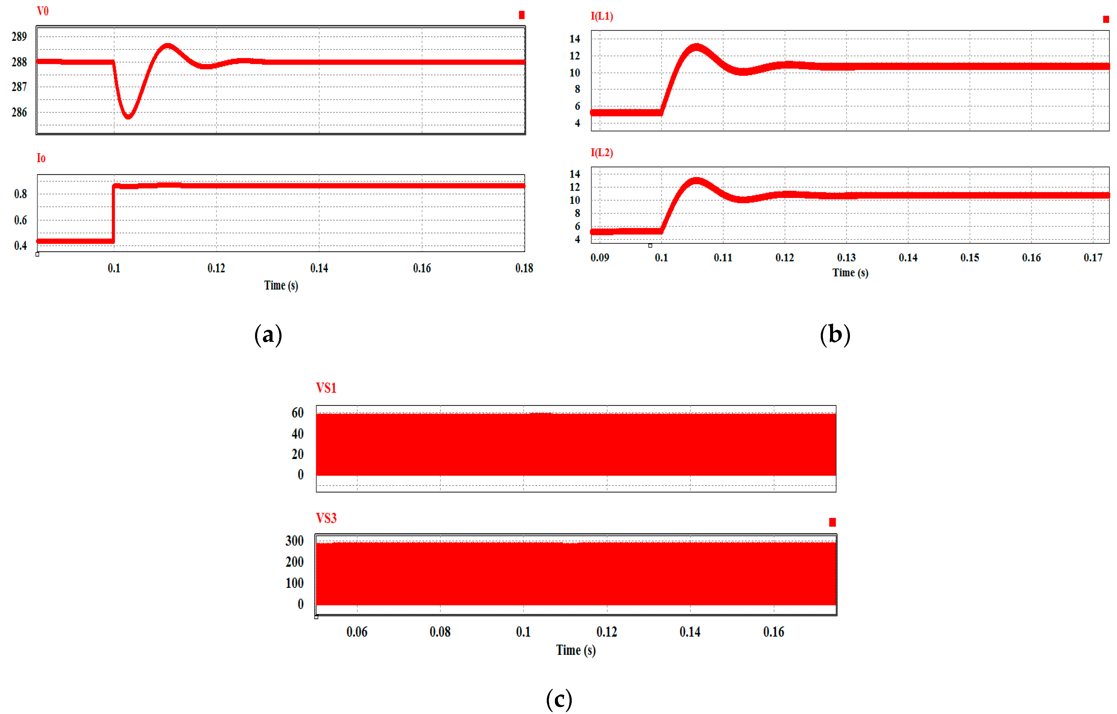
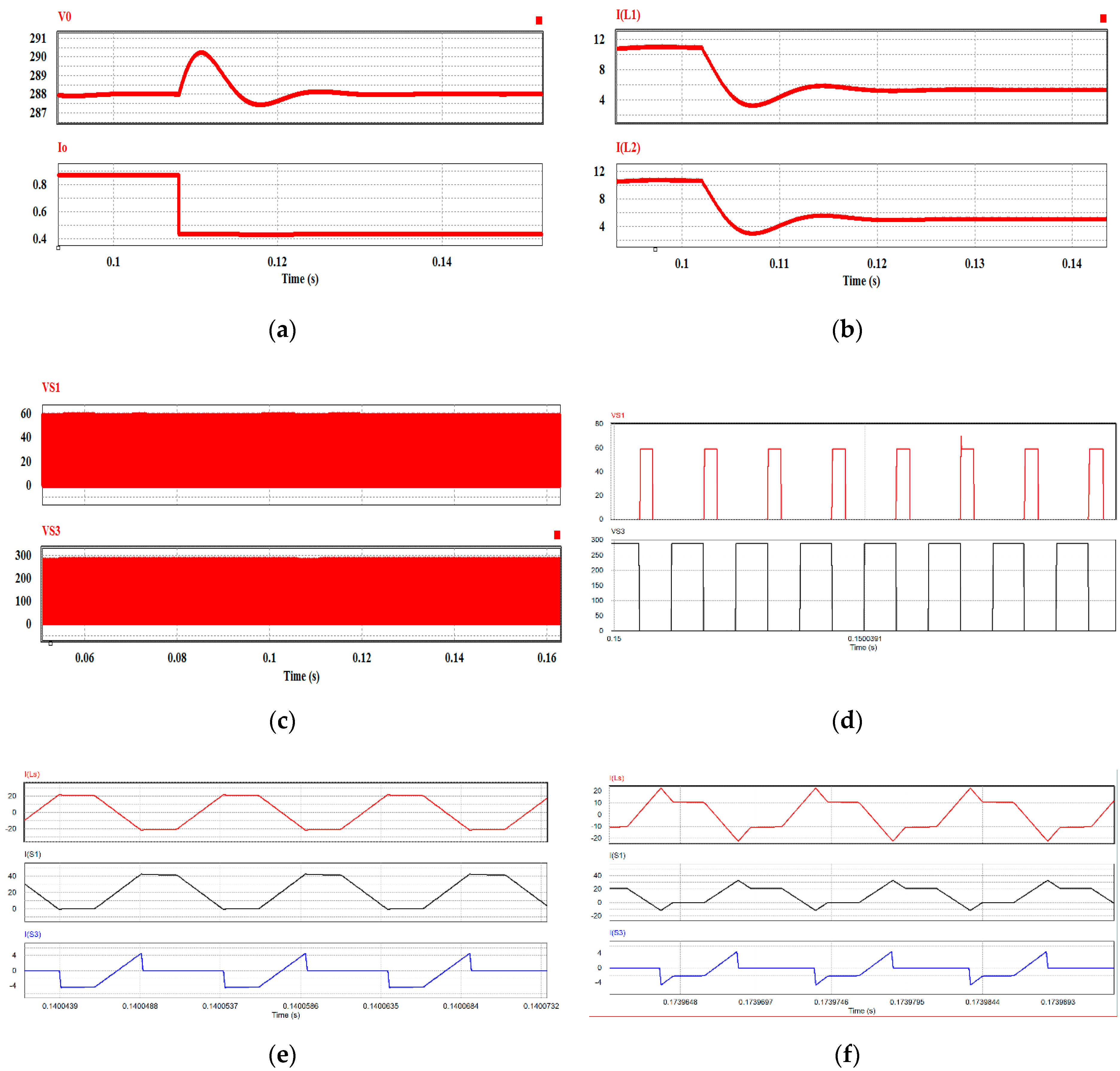
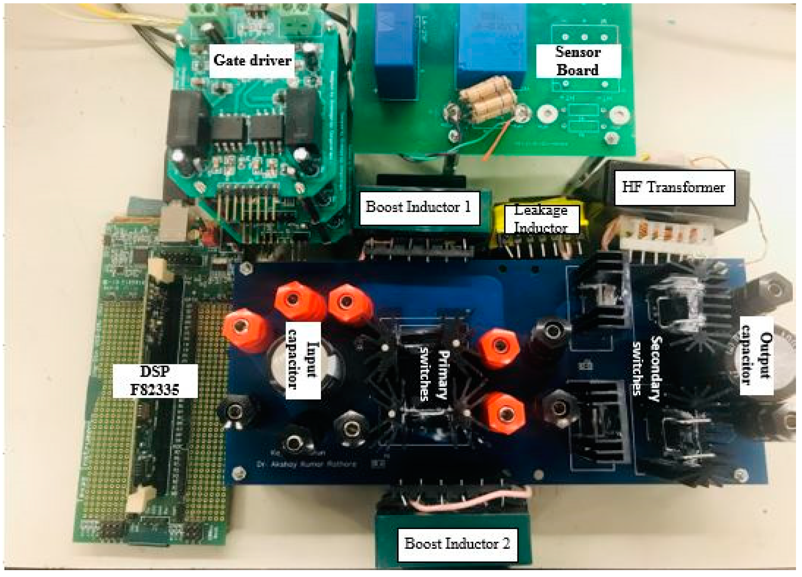
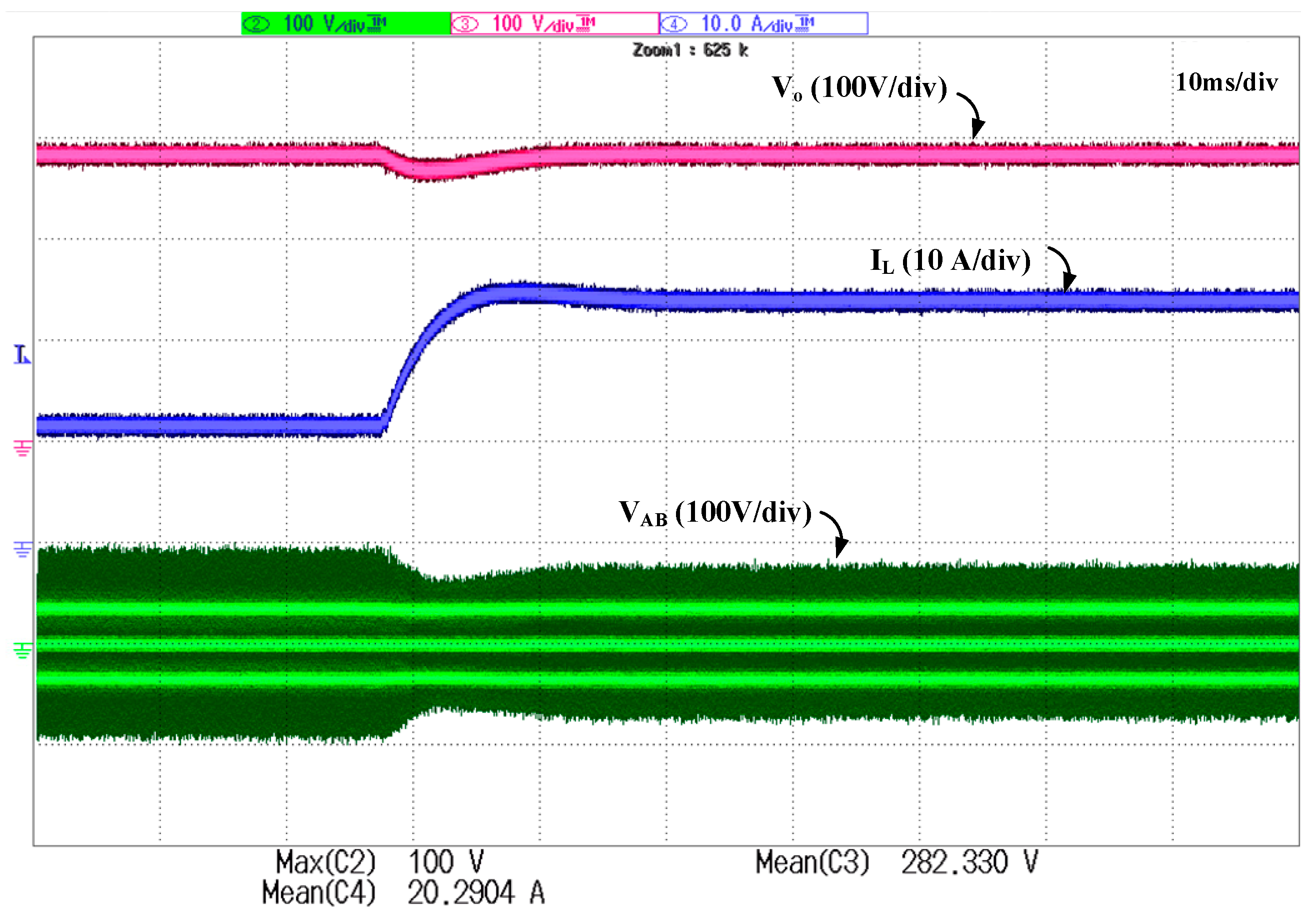
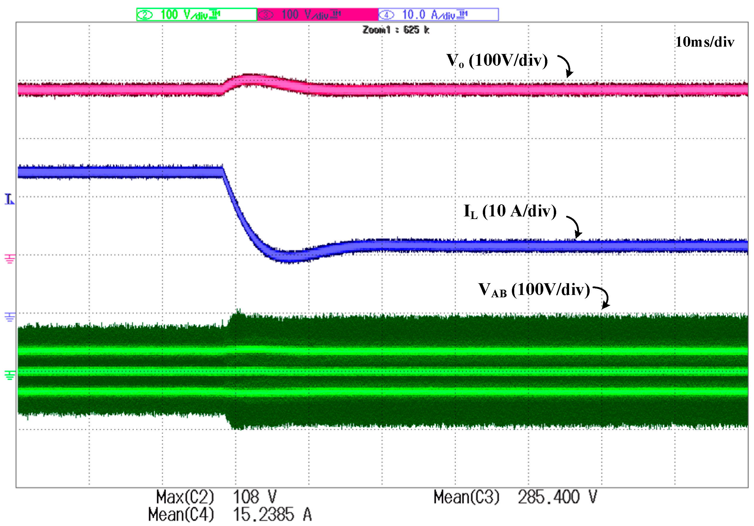
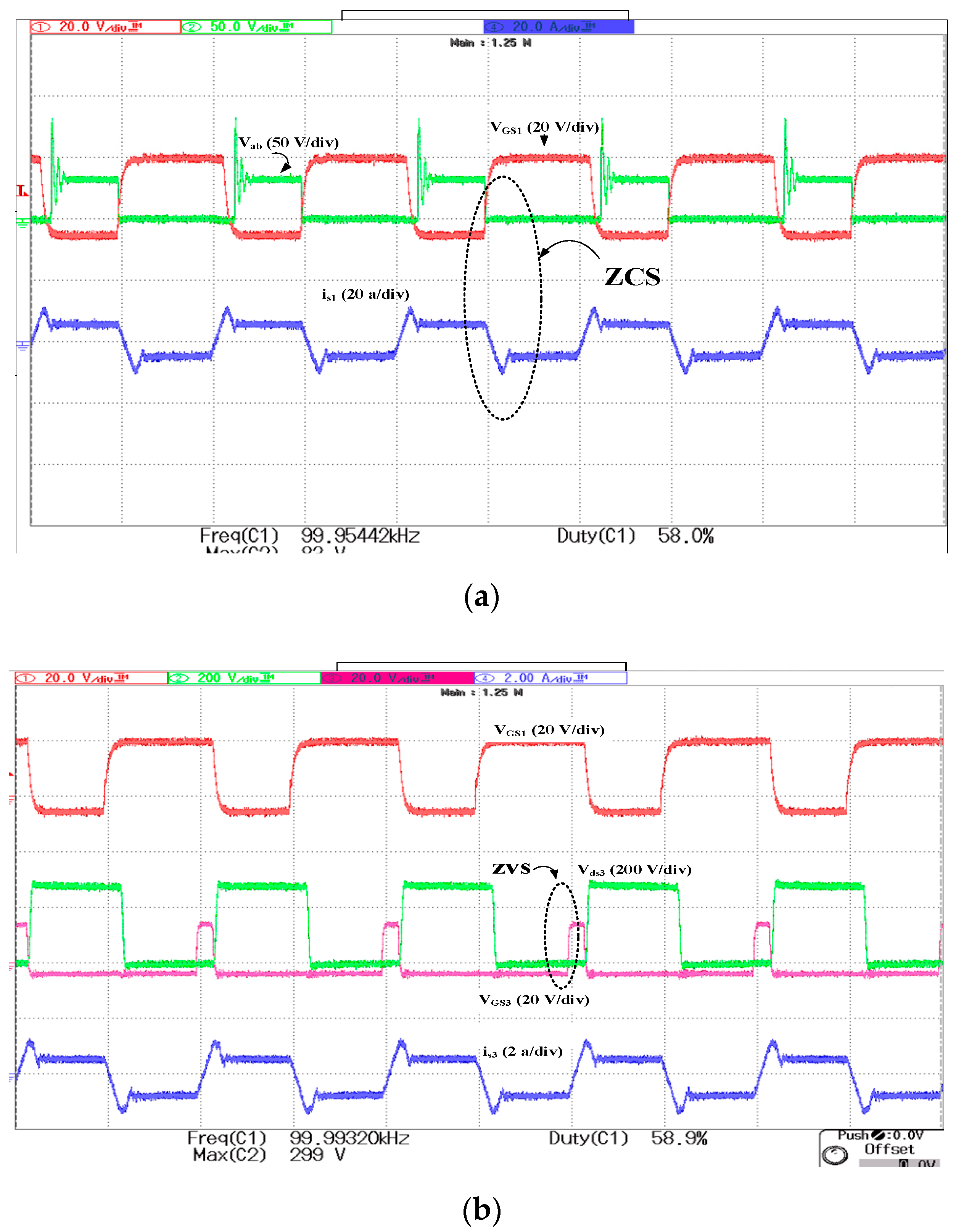
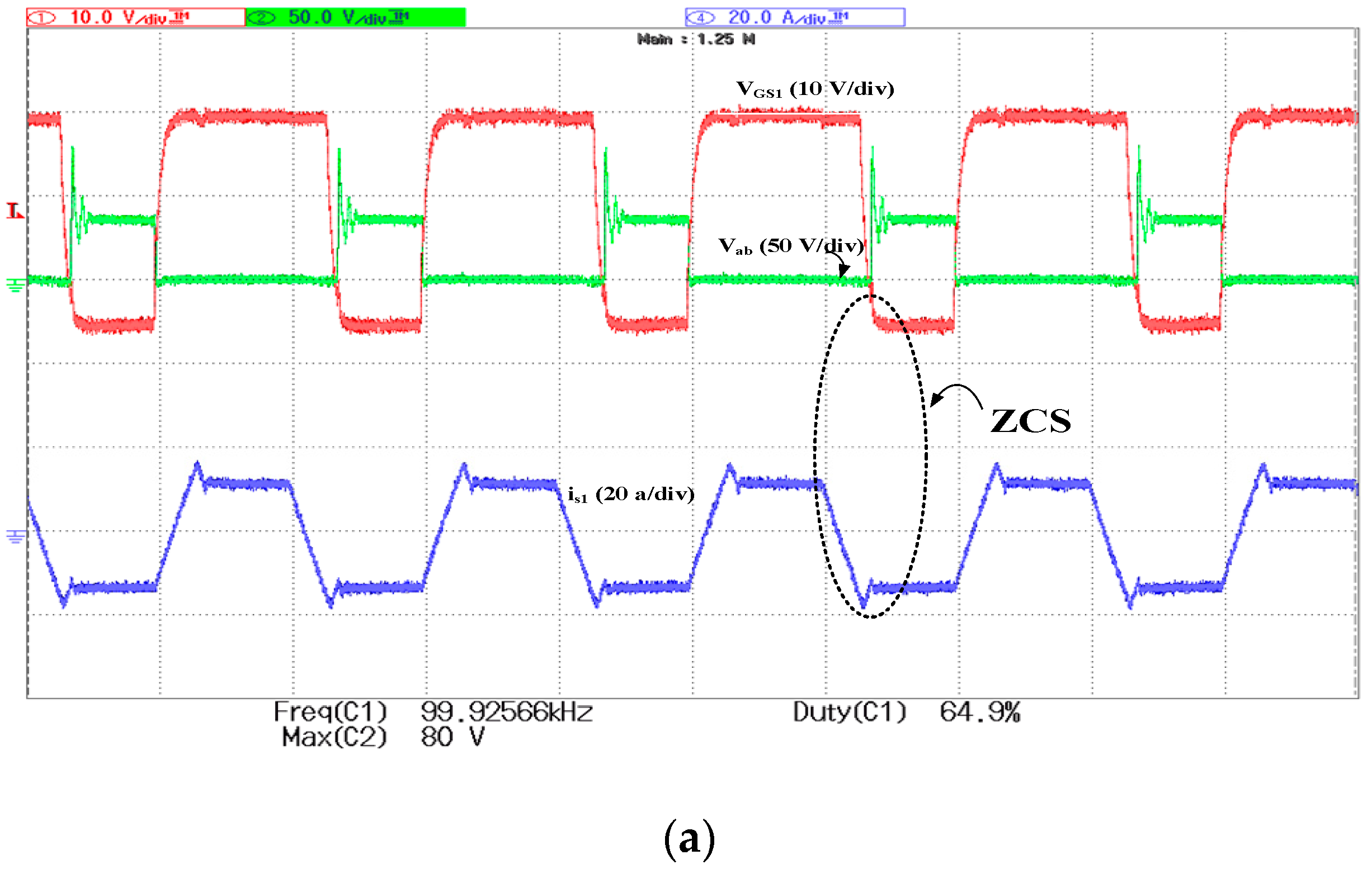
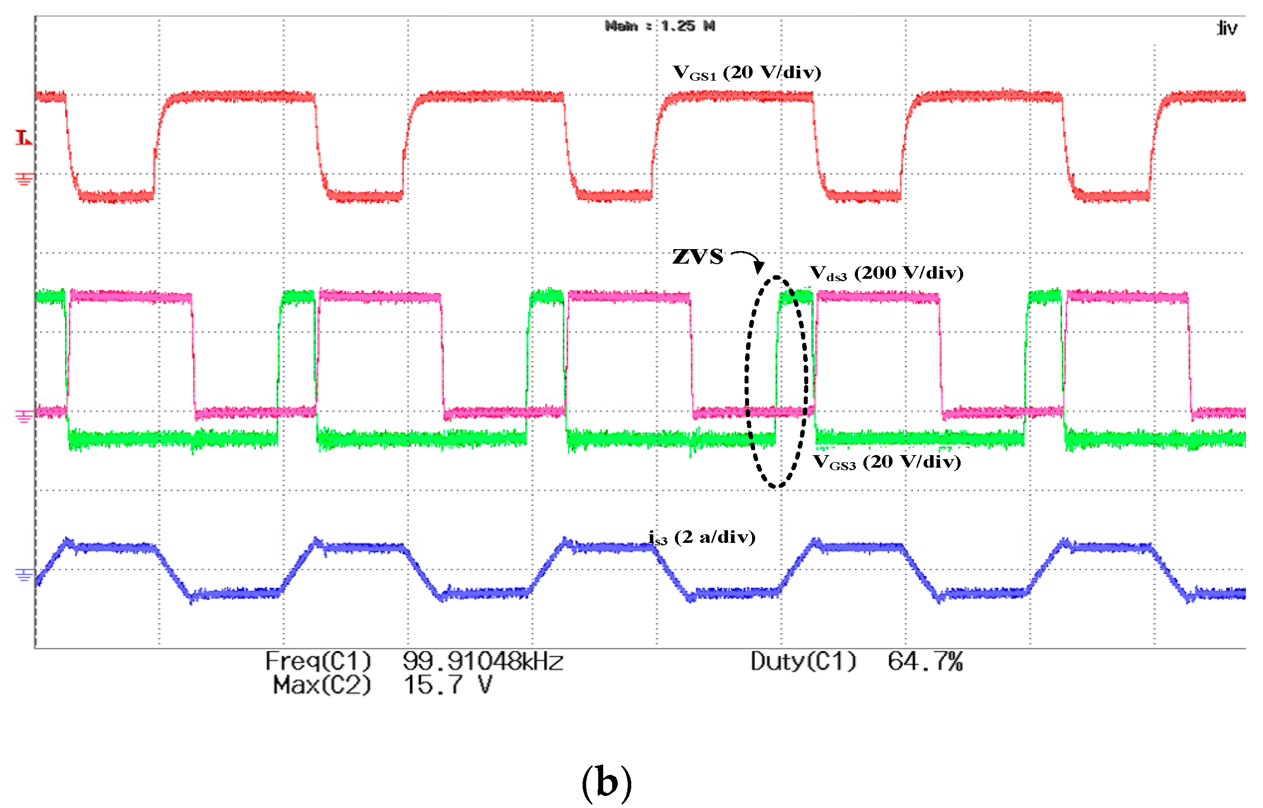
4. Simulation and Experimental Results

The simulation model of the circuit topology and two-loop control was developed on software package PSIM 11 and was run to capture waveforms and observe transient performance of the converter under load-current variations. Simulation results are illustrated in Figure 13 and Figure 14.
The load is changed from 50% load to rated load (Figure 13) and from full load to 50% load (Figure 14). It should be observed that the overshoot or undershoot in output voltage for both step changes is 2V, which demonstrates the excellent stability of control. Load current and the two input inductor currents smoothly change to the next steady-state value. The settling time of the inductors’ current and load voltage is nearly 25 ms. The voltage across the primary switches (VS1) is clamped at the reflected output voltage, and the voltage across the secondary devices (VS3) is clamped at the output voltage Vo without any overshoot during the load transients, ensuring safe operation of the converter. Figure 14d (zoomed waveform in transient period) shows voltage across the primary side devices is clamped at the reflected output voltage, while voltage on the secondary side devices is always clamped at output voltage. Figure 14e,f shows steady-state (zoomed) waveforms at rated load and half load, respectively. It should be noted that primary side devices maintain ZCS, and secondary side devices maintain ZVS under both conditions.
Figure 15 shows the experimental prototype of the converter. It is operated by the designed controller, which has been tested in the laboratory for the step changes in load for a fixed 12 V input voltage. Table 2 shows the details of the components used in the hardware prototype.
Gating signals for the semiconductor devices are generated by Texas Instruments (TI) digital signal processor (DSP) TMS320F28335. Experimental waveforms for the step change in load are shown in Figure 16 and Figure 17. Figure 16 demonstrates the experimental waveforms of inductor current iL, voltage VAB, and output voltage Vo with respect to time for the step change in load from rated load to 50% load. The similar waveforms for step change in load from 50% to rated load are manifested in Figure 17. Overshoot and undershoot in the output voltage are negligible during load transients. Further, output voltage V o is maintained at the constant value. The variations in inductor current I L and V A B (transformer primary voltage, that is, the sum of voltage across the two primary switches S1 and S2) are within safe limiting values. Therefore, the switches do not experience any voltage spike during transition, which ensures safe and normal operation of the converter. Inductor current I L is adjusted to their new steady-state values smoothly. The settling time is nearly 20 ms. This demonstrates stable performance over a wide load variation. It should be noticed that the experimental settling time is higher than the simulation value because the hardware experiences power loss, voltage drop, stray inductance/capacitance, system delay, and parasitic elements, which cause aberration from the ideal model. Better dynamic performance may be achieved by proper tuning of the controller parameters.
Figure 18 and Figure 19 show the steady-state zoomed waveforms under half load and full load, respectively. Figure 18a and Figure 19a show the gate-to-source V G S and drain-to-source Vds voltage waveforms across primary side MOSFET and transformer primary current is waveform at half load and full load, respectively. It is clearly demonstrated that the current through the switch naturally goes to zero. The negative current shows the antiparallel body diode conduction across the switch before turning off the gating signals, ensuring ZCS turn-off of the primary side semiconductor devices.
Voltage waveforms VGS and VDS across the devices clearly demonstrate the ZCS of the primary side devices and ZVS of the secondary side devices under both load conditions. The results are satisfactory during the transients that occurred due to sudden load disturbances while maintaining the steady-state performance. The steady-state performance is retained at the originally proposed in [17]. Corresponding gate-to-source   V G S and drain-to-source voltage V d s waveforms of the secondary side devices are shown in Figure 18b and Figure 19b. In these waveforms, gate-to-source voltage ( V G S ) is applied when the voltage across secondary device VDS is zero already, which ensures ZVS operation in secondary devices. It confirms the soft-switching of all the devices.
Table 3 shows the comparison between the conventional active-clamped converter and the proposed snubberless topology. It is clear from the comparison that the snubberless operation with proposed control has several merits in terms of voltage gain, efficiency, reduced current, transformer size, and soft-switching range. Simple control has resulted in these merits with a demerit of limited duty range.

5. Conclusions

This paper studied small-signal modeling and derived transfer functions of an isolated naturally clamped snubberless current-fed half-bridge DC-DC converter. A two-loop average current controller was designed offering fixed-frequency duty cycle modulation of the semiconductor devices using two controllers. Initial verification of the small-signal model and the controller was done using PSIM 11 and investigation of the dynamic performance of the converter. Experimental results on a laboratory hardware proof-of-concept prototype demonstrated the satisfactory and smooth transient performance of the converter and the effectiveness of the designed closed-loop controller. The simplicity of implementation and practicality of the proposed control are the benefits of the overall system. The proposed analysis is effective for non-isolated as well as interleaved half-bridge and interleaved-boost topologies. It is suitable for fuel cell applications.

Author Contributions

Formal analysis, K.K.; Funding acquisition, A.K.R.; Methodology, K.K., V.V.R., and B.L.N.; Project administration, V.V.R.; Resources, A.K.R.; Software, B.L.N.; Supervision, A.K.R.; Validation, K.K. and V.V.R.; Writing—original draft, K.K. and V.V.R.; Writing—review and editing, A.K.R. and B.L.N. All authors have read and agreed to the published version of the manuscript.

Funding

This research was funded by the Natural Sciences and Engineering Research Council of Canada (NSERC), grant number N01678.

Acknowledgments

The authors would like to acknowledge the support of the National Institute of Technology, Warangal, India and the support of Scheme for Promotion of Academic and Research Collaboration (SPARC) funded by MHRD, Government of India with file no SPARC/2018-2019/P1392/SL. SPARC, India.

Conflicts of Interest

The authors declare no conflict of interest.

References

  1. Aso, S.; Kizaki, M.; Nonobe, Y. Development of hybrid fuel cell vehicles in Toyota. In Proceedings of the IEEE Power Conversion Conference, Nagoya, Japan, 2–5 April 2007; pp. 1606–1611. [Google Scholar]
  2. Emadi, A.; Williamson, S.S. Fuel cell vehicles: Opportunities and challenges. In Proceedings of the IEEE Power Engineering Society General Meeting, Denver, CO, USA, 6–10 June 2004; pp. 1640–1645. [Google Scholar]
  3. Emadi, A.; Rajashekara, K.S.; Williamson, S.S.; Lukic, S.M. Topological overview of hybrid electric and fuel cell vehicular power system architectures and configurations. IEEE Trans. Veh. Technol. 2005, 54, 763–770. [Google Scholar] [CrossRef]
  4. Khaligh, A.; Li, Z. Battery, Ultracapacitor, FuelCell, and Hybrid Energy Storage Systems for Electric, Hybrid Electric, FuelCell, and Plug-In Hybrid Electric Vehicles: State of the Art. IEEE Trans. Veh. Technol. 2010, 59, 2806–2814. [Google Scholar] [CrossRef]
  5. Rathore, A.K.; Bhat, A.K.S.; Oruganti, R. Analysis, Design and Experimental Results of Wide Range ZVS Active-Clamped L-L Type Current-Fed DC/DC Converter for Fuel Cells to Utility Interface. IEEE Trans. Ind. Electron. 2011, 59, 473–485. [Google Scholar] [CrossRef]
  6. Wu, T.-F.; Chen, Y.-C.; Yang, J.-G.; Kuo, C.-L. Isolated bidirectional full-bridge DC–DC converter with a flyback snubber. IEEE Trans. Power Electron. 2010, 25, 1915–1922. [Google Scholar]
  7. Su, G.-J.; Adams, D.J.; Peng, F.Z.; Li, H. Experimental evaluation of a soft-switching DC/DC converter for fuel cell vehicle applications. In Proceedings of the Power Electronics in Transportation, Auburn Hills, MI, USA, 24–25 October 2002; pp. 39–44. [Google Scholar]
  8. Song, W.; Lehman, B. Current-fed dual-bridge DC–DC converter. IEEE Trans. Power Electron. 2007, 22, 461–469. [Google Scholar] [CrossRef]
  9. Averberg, A.; Meyer, K.R.; Mertens, A. Current-fed full-bridge converter for fuel cell systems. In Proceedings of the IEEE Power Electronics Specialists Conference, Rhodes, Greece, 15–19 June 2008; pp. 866–872. [Google Scholar]
  10. Yakushev, V.; Meleshim, V.; Fraidlin, S. Full bridge isolated current fed converter with active-clamp. In Proceedings of the IEEE Applied Power Electronics Conference, Dallas, TX, USA, 14–18 March 1999; pp. 560–566. [Google Scholar]
  11. Rathore, A.K.; Prasanna, U.R. Comparison of soft-switching voltage-fed and current-fed bi-directional isolated Dc/Dc converters for fuel cell vehicles. In Proceedings of the IEEE International Symposium on Industrial Electronics, Hangzhou, China, 28–31 May 2012; pp. 252–257. [Google Scholar]
  12. Zhu, L. A Novel Soft-Commutating Isolated Boost Full-bridge ZVS-PWM DC-DC Converter for Bi-directional High Power Applications. In Proceedings of the 2004 IEEE 35th Annual Power Electronics Specialists Conference, Aachen, Germany, 20–25 June 2004; Volume 21, pp. 422–429. [Google Scholar]
  13. Kim, E.S.; Joe, K.Y.; Choi, H.Y.; Kim, Y.H.; Cho, Y.H. An Improved Soft Switching Bi-directional PSPWM FB DC/DC Converter. In Proceedings of the IEEE Industrial Electronics Conference, Aachen, Germany, 31 August–4 September 1998; pp. 740–743. [Google Scholar]
  14. Miura, Y.; Kaga, M.; Horita, Y.; Ise, T. Bidirectional Isolated Dual Full-bridge dc-dc Converter with Active Clamp for EDLC. In Proceedings of the IEEE Energy Conversion Congress and Exposition, Atlanta, GA, USA, 12–16 September 2010; pp. 1036–1143. [Google Scholar]
  15. Wang, K.; Lin, C.Y.; Zhu, L.; Qu, D.; Lee, F.C.; Lai, J.S. Bidirectional DC/DC Converters for Fuel Cell Systems. In Proceedings of the IEEE Power Electronics in Transportation, Dearborn, MI, USA, 22–23 October 1998; pp. 47–51. [Google Scholar]
  16. Wang, K.; Lee, F.C.; Lai, J. Operation Principles of Bi-directional Full-bridge DC/DC Converter with Unified Soft switching Scheme and Soft-starting Capability. In Proceedings of the IEEE Applied Power Electronics Conference and Exposition, New Orleans, LA, USA, 6–10 February 2000; pp. 111–118. [Google Scholar]
  17. Rathore, A.K.; Prasanna, U.R. Analysis, design, and experimental results of novel snubberless bi-directional naturally clamped ZCS/ZVS current-fed half-bridge dc/dc converter for fuel cell vehicles. IEEE Trans. Ind. Electron. 2013, 60, 4482–4491. [Google Scholar] [CrossRef]
  18. Khatun, K.; Rathore, A.K. Small Signal Modeling, Closed Loop Design, and Transient Results of Snubberless Naturally-Clamped Soft-Switching Current-Fed Half-bridge DC/DC Converter. In Proceedings of the IEEE International Symposium on Industrial Electronics (ISIE), Vancouver, BC, Canada, 12–14 June 2019; pp. 2571–2576. [Google Scholar]
  19. Lai, J.; Park, S.; Moon, S.; Chen, C.L. A High-Efficiency 5-kW Soft-Switched Power Conditioning System for Low-Voltage Solid Oxide Fuel Cells. In Proceedings of the IEEE Power Conversion Conference-Nagoya, Nagoya, Japan, 2–5 April 2007; pp. 463–470. [Google Scholar]
  20. Venkatraman, R.; Bhat, A.K.S. Small-signal analysis of a soft-switching, single-stage two-switch AC-to-DC converter. In Proceedings of the IEEE Power Electronics Specialists Conference, Vancouver, BC, Canada, 17–21 June 2001; pp. 1824–1830. [Google Scholar]
  21. Krein, P. Elements of Power Electronics, 2nd ed.; Oxford University Press: Oxford, UK, 2014. [Google Scholar]
  22. Bibian, S.; Jin, H. High performance predictive dead-beat digital controller for DC power supplies. IEEE Trans. Power Electron. 2002, 17, 420–426. [Google Scholar] [CrossRef]
  23. Erickson, R.; Madigan, M.; Singer, S. Design of a simple high-power-factor rectifier based on the flyback converter. In Proceedings of the IEEE Applied Power Electronics Conference and Exposition (APEC), Los Angeles, CA, USA, 11–16 March 1990; pp. 792–801. [Google Scholar]
Figure 1. The zero current switching (ZCS) naturally clamped current-fed half-bridge isolated DC-DC converter. Reproduced with permission from [17], IEEE, 2020.
Applsci 10 06130 g001
Figure 2. Operating waveforms of the ZCS current-fed converter shown in Figure 1. Reproduced with permission from [17], IEEE, 2020.
Applsci 10 06130 g002
Figure 3. Equivalent circuits during different intervals of the operation for the waveform in Figure 2 Reproduced with permission from [17], IEEE, 2020. (a) S2 in blocking mode; (b) S2 is turned-on; (c) ZVS turn-on of S4 and S5; (d) ZCS turn-off of S1 and body diode conducts; (e) D3 and D6 start conduction for rectification; (f) S1 goes in blocking mode.
Applsci 10 06130 g003aApplsci 10 06130 g003b
Figure 4. Complete two-loop average current control block diagram.
Applsci 10 06130 g004
Figure 5. The control-to-output voltage transfer function of the system.
Applsci 10 06130 g005
Figure 6. Pole-zero map of the control-to-output voltage transfer function of the system without controller.
Applsci 10 06130 g006
Figure 7. Inner current control loop schematic diagram.
Applsci 10 06130 g007
Figure 8. Bode plot of compensated control to input current transfer function: phase margin (PM) = 90 ° at 177 k rad/s.
Applsci 10 06130 g008
Figure 9. Bode plot of compensated control to input current transfer function: PM = 59.8 ° at 31.5 k rad/s (5000 Hz).
Applsci 10 06130 g009
Figure 10. Outer voltage control loop schematic diagram.
Applsci 10 06130 g010
Figure 11. Bode plot of uncompensated plant in voltage control loop: PM = 94.1 ° at 1990 rad/s.
Applsci 10 06130 g011
Figure 12. Bode plot of the compensated voltage control loop system: PM = 60 ° at 3150 rad/s (500 Hz).
Applsci 10 06130 g012
Figure 13. Simulation waveforms for Vin = 12 V with step change in load from 50% load to rated full load; (a) Vo is output voltage, Io is output current, (b) IL1 and IL2 are input inductor currents, and (c) Vs1 and Vs3 are voltages across the switches S 1 and S 3 , respectively.
Applsci 10 06130 g013
Figure 14. Simulation waveforms for Vin = 12 V with step change in load from rated load to half load with identical nomenclature. (a) Vo is output voltage, Io is output current, (b) IL1 and IL2 are input inductor currents, and (c) Vs1 and Vs3 are voltages across the switches S 1 and S 3 , respectively, (d) zoomed waveform of Vs1 and Vs3, (e). ILs is the transformer primary current and IS1 and IS2 are the current through the switches S 1 and S 3 , respectively at full-load steady-state and (f) ILs is the transformer primary current and IS1 and IS2 are the current through the switches S 1 and S 3 , respectively at half-load steady-state.
Applsci 10 06130 g014
Figure 15. Laboratory prototype of the half-bridge converter.
Applsci 10 06130 g015
Figure 16. Hardware result for step change in load from 50% load to full load: (1) voltage VAB (100 V/div), (2) inductor current iL (10 A/div), and (3) output voltage Vo (100 V/div).
Applsci 10 06130 g016
Figure 17. Hardware result for step change in load from full load to 50% load: (1) voltage VAB (100 V/div), (2) inductor current iL (10 A/div), and (3) output voltage Vo (100 V/div).
Applsci 10 06130 g017
Figure 18. Experimental results for v i n = 12 V at 50% load: (a) gate-to-source voltage V G s 1   ( 20   V / div ) , current across primary-side MOSFET is1 (20 A/div), and voltage V A B = 50 V/div; (b) gate-to-source voltage V G S 3 (20 V/div), drain-to-source voltage V d s 3 (200 V/div), and current across secondary-side MOSFET is3 (2 A/div).
Applsci 10 06130 g018
Figure 19. Experimental results for v i n = 12 V at full load: (a) gate-to-source voltage V G s 1   ( 20   V / div ) , current across primary-side MOSFET is1 (20 A/div), and voltage V A B = 50 V/div; (b) gate-to-source voltage V G S 3 (20 V/div), drain-to-source voltage V d s 3 (200 V/div), and current across secondary-side MOSFET is3 (2 A/div).
Applsci 10 06130 g019aApplsci 10 06130 g019b
Table 1. Design specifications for the control system of the converter.
Input voltage V i n 12 V
Output Voltage V o 288 V
Peak output power P o 250 W
Switching frequency converter f s 100 kHz
Leakage inductor L l s 1.74 μH,
Input Boost Inductors L 200 μH,
Output Capacitor C O 220 μF
Full-load R L 331.77 Ω.
Table 2. Component parameters of the hardware prototype.
ComponentsParameters
Primary Switch ( S 1 ,   S 2 ) IRFB4127PbF 200 V, 76 A, R d s , o n = 17 mΩ
Secondary Switch ( S 3 ,   S 4 ) IPP60R125CP 650 V, 11 A, R d s , o n = 0.125 Ω
Series InductorTDK5901PC40Z core, 3.9 μH
HF transformer3C95ETD49 ferrite core; N 1 = 5, N 2 = 45
Boost Inductors3C95ETD49 ferrite core, N = 42 , L = 200 μH
Output Capacitor C O 220 μF, 450 V electrolytic capacitor
0.68 μF, 450 V high frequency film capacitor
Table 3. Comparison of proposed snubberless topology with active-clamped topology.
TopologyActive-ClampedProposed Snuberless
Soft-switchingZVS
(soft-switching at turn-on)
ZCS
(soft-switching at turn-off)
Soft-switching rangeLimited range
(soft-switching is lost with the source voltage variation)
Full range
(inherent soft-switching for the entire operating range)
Device voltageHigher voltage and variable with duty cycleClamped at reflected output voltage and duty cycle independent
Boost Capability (voltage gain)Voltage gain (boost) is compromised; 20% reduction at rated loadNatural boost gain
Device RMS currentCirculating current is present that increases average and RMS value10% reduction in the rms current due to the absence of active clamp
Device peak current1.5× input currentSame as input current (33% less)
Transformer currentSame as input currentHalf of the input current (50% less)
EfficiencyHigh2% improvement
Power flowUnidirectionalBidirectional
Duty cycle variationWide range (0 to 1)Limited (0.5 to 1)
TransformerHigher turns ratio, higher kVA rating and volumeRelatively lower turns ratio, reduced kVA rating and volume (40% less)

