1. Introduction
The physics and applications of ultra-nanocrystalline diamond (UNCD) films have been and are currently being investigated due to their unique combination of properties such as: high wear resistance [
1], highest hardness relative to any other films [
1], lowest friction coefficient [
1] compared with metal and ceramic coatings chemical inertness to corrosion [
1], negative electron affinity low work function for electron emission [
1], high electrical conductivity via boron (B) atoms doping of UNCD producing B-UNCD films [
2,
3], N atom insertion into grain boundaries of UNCD films, producing the N-grain boundary incorporated ultrananocrystalline diamond (N-UNCD) films, as previously demonstrated by different groups worldwide experimentally [
4,
5,
6,
7,
8], and theoretically [
9]. The combination of these properties makes doped UNCD films suitable for many applica-tions like corrosion resistant electrically conductive B-UNCD coatings on metal electrodes, for electrolysis-based water purification systems [
3] and Li-ion batteries electrodes, thermionic and field emission devices, and high-power electronic devices [
2,
10]. The R&D described in this paper focused on exploring the effect of total pressure and microwave power on the electrical conductivity of N-UNCD films grown by microwave plasma chemical vapor deposition (MPCVD) in order to maximize the electrical conductivity of these films.
Zaitsev et al. [
11] recently demonstrated to dope the diamond with nitrogen using the CVD technique, however, our research is novel because we use the MPCVD technique and the diamond size scale that we produce is much smaller.
2. Materials and Methods
The N-UNCD films were grown by the MPCVD technique, using an IPLAS MPCVD system with a microwave frequency of 915 MHz. The growth conditions were as follows: (i) SiO2/Si and Si substrates were used; (ii) A mixture of Ar (78 sccm)/CH4 (2 sccm)/N2 (20 sccm) gases were flown in a chamber evacuated to ~10−7 Torr, while applying microwave power (see values below) to ionize atoms and molecules and produce a plasma; (iii) all films were grown for 2 h. The substrates were heated to temperatures in the range 717–880 °C, with the surface temperature measured by a pyrometer focused on the substrate surface.
Three experimental film growth series were carried out, varying the total pressure in the film growth chamber and the microwave power, respectively, as shown in
Table 1, to study the impact of these parameters on the electrical conductivity of the N-UNCD films, in order to determine the optimal conditions.
The total pressure was varied between 70, 80, 90, and 100 mbar while the microwave power was maintained at 3000, 4000, and 4500 W for each experimental series, respectively.
3. Results
The N-UNCD films were characterized by X-ray diffraction (XRD), using a Rigaku diffractometer (Ultima III, Cu Kα radiation, 1.524 A), scanning electron microscopy (SEM, Zeiss- SUPRA-40) -Thornwood-New York, X-ray photoelectron spectroscopy (XPS-PHI 5000 Versa Probe II-ULVAC), and, Raman spectroscopy (Thermo Scientific-DXR, 532 nm wavelength LASER Beam). XRD, SEM, XPS, and Raman analysis were done to determine the films crystalline structure, morphology, film thickness, grain boundary structure, and to confirm the presence of N atoms, respectively. Four-point probe measurements were done to determine the electrical conductivity of the N-UNCD films grown through different conditions and correlate it with the characterized properties provided by the analytical techniques described above.
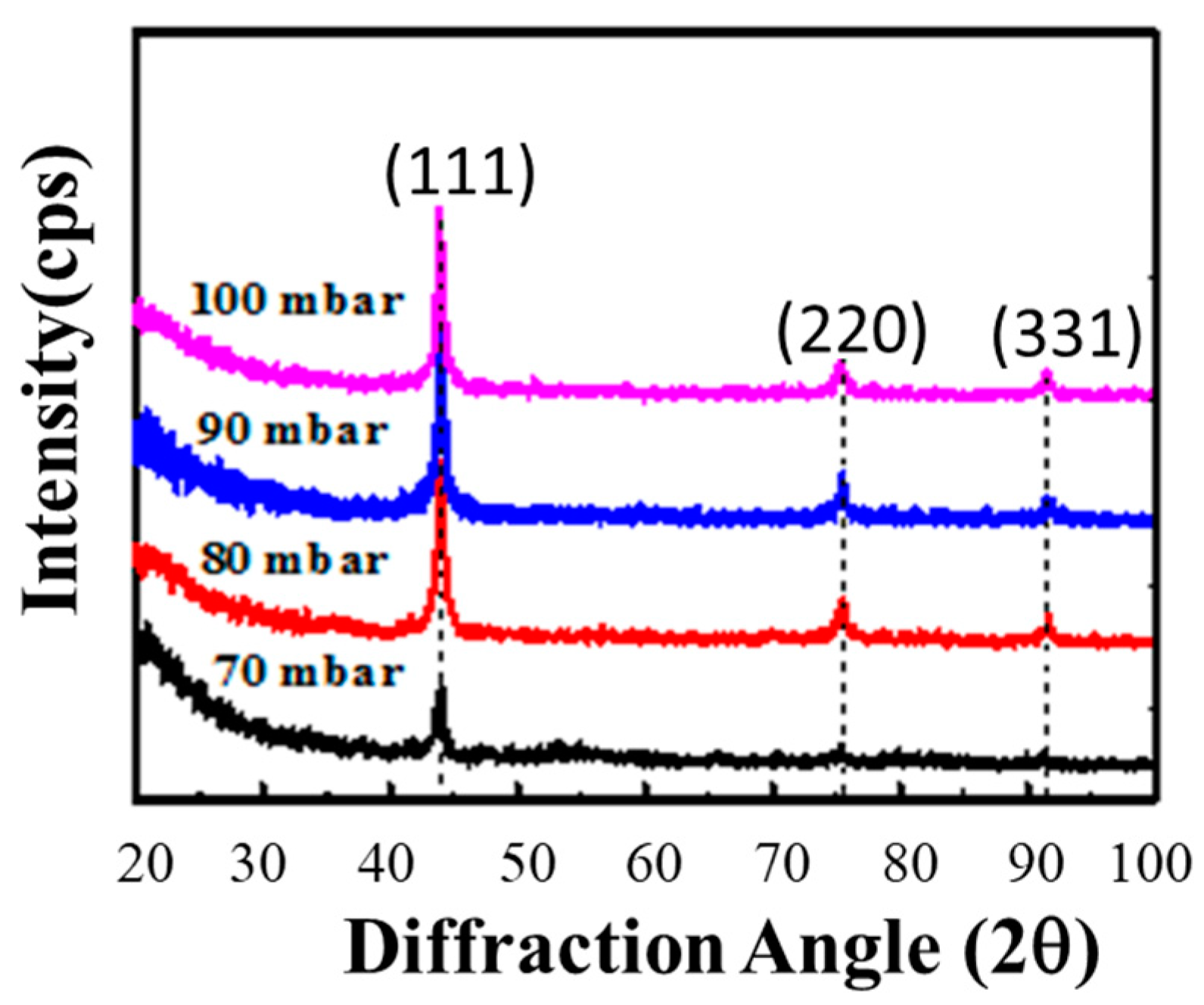
Figure 1 shows the XRD analysis results from the series 3 N-UNCD films, wherein for all N-UNCD films the preferential orientation correspond to the diamond (111) planes. This measurement was performed in a 2Theta configuration.
The XRD diffractograms show only the peaks attributed to diamond at 43.9° (111), 75.4° (220) and 91.7° (331), indicating that the films are composed mostly by sp3 diamond-type bonded C atoms without any graphite phase, as determined using specific software [
12].
Table 2 shows the calculated grain sizes of the N-UNCD films (using the Scherrer–Debye equation), resulting in estimated grain sizes of 7 to 9 nm for all cases, consistent with the N-UNCD grain sizes reported in prior work for N-UNCD films produced by MPCVD [
4].
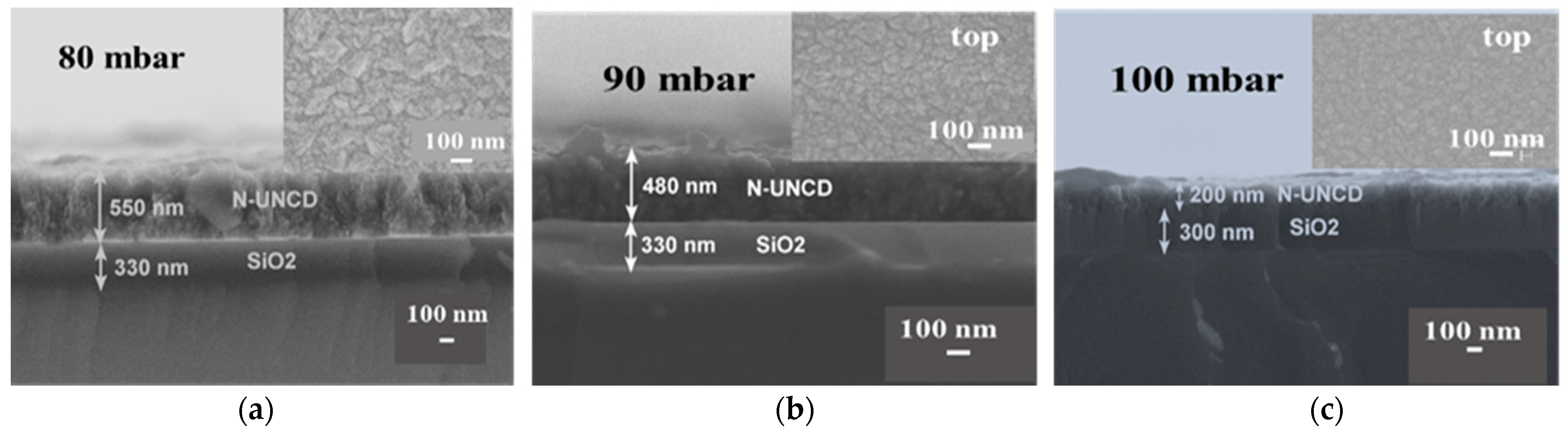
Figure 2a–c show SEM micrographs (top view and cross section) of N-UNCD films grown at different total pressures, using the same microwave power, revealing smooth morphology composed of many agglomerates as is expected for N-UNCD films [
1,
4]. The SEM cross section images show film thicknesses of 550, 480, and 200 nm for the N-UNCD films grown at 80, 90, and 100 mbar with 4500 W power, respectively.
This indicates that the growth rate decreases as the pressure increases. The N-UNCD films thickness decrease as a function of growth pressure could be due to a reduction in arrival of C2 dimers and CHx radicals-growth species, due to collision with other molecules and atoms in the plasma, and reduction in plasma area, which occurs as the total pressure increases, resulting in the substrate not getting fully covered by the plasma at high pressures.
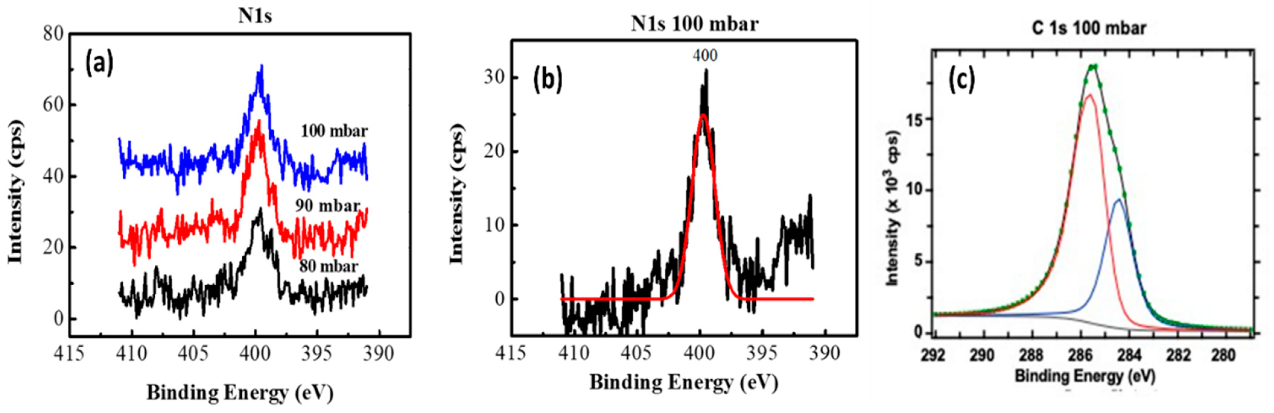
Figure 3 show the XPS spectra, for: (a) N 1s peak observed from N-UNCD films grown at different total pressures, using the same microwave power; (b) N 1s peak and (c) C 1s peak for N-UNCD film grown at 100 mbar and 4500 W. Two peaks form the C 1s signal, as indicated by in situ XPS computer simulation, showing peaks at 284.4 and 285.5 eV. The peak at 285.5 eV is attributed to carbon atoms with the sp3 bonds of diamond [
13], while the peak at 284.4 eV is due to Argon atoms incorporation in the diamond lattice as a byproduct of cleaning the sample of surface contaminants with Ar+ ion bombardment prior to XPS analysis [
14]. The peak at 286.6 eV is attributed to a C=N bond and to the formation of a carbide respectively [
13]. The XPS spectra for the N-UNCD film in the N1s region (
Figure 3b) shows a relatively weak but clear signal correlated with a single peak at 400 eV, confirming the presence of nitrogen in the N-UNCD films [
7].
Figure 4 shows the Raman spectra of N-UNCD films grown at: (a) 3000 W, (b) 4000 W, and (c) 4500 W. The spectra exhibit the characteristic bands of N-UNCD reported in the literature, which are the G band at 1550 cm
−1 attributed to sp2 carbon bonds, and the D band at 1350 cm
−1 attributed to disorder-induced sp2 carbon bonds in grain boundaries. The D band at 1350 cm
−1 encapsulate the 1332 cm
−1 peak, which is the finger-print of diamond.
In addition, the bands at 1450 cm
−1 and 1130 cm
−1 correspond to C=C and C-H bonds in transpoliacetilene (TPA) molecules, respectively, reported in [
15,
16]. The intensity of the TPA peaks (1130 and 1450 cm
−1), in the Raman spectra of the N-UNCD films, decreased as the total pressure and microwave power increased during film growth. This indicates that the grain boundary chemistry of the N-UNCD films presents more sp2 bonded carbon atoms and less TPA bonds with an increase in the total pressure and microwave power. This could be due to a higher incorporation of N atoms, as the total pressure and microwave power increases, since C-N bonds compete with TPA bonds in the grain boundaries as N atoms are getting incorporated.
Figure 4d shows the substrate temperature vs. film grown pressure. The decrease in the intensities of the TPA bands, previously discussed, is correlated with an increase in the substrate temperature, obtaining a maximum substrate temperature for the film grown at 100 mbar and 4500 W, which is also the N-UNCD film with the lowest TPA bands intensities. These results are consistent with publications in the literature, which also show lower TPA Raman signals as the substrate temperature increases during the growth of UNCD and N-UNCD films [
17,
18].
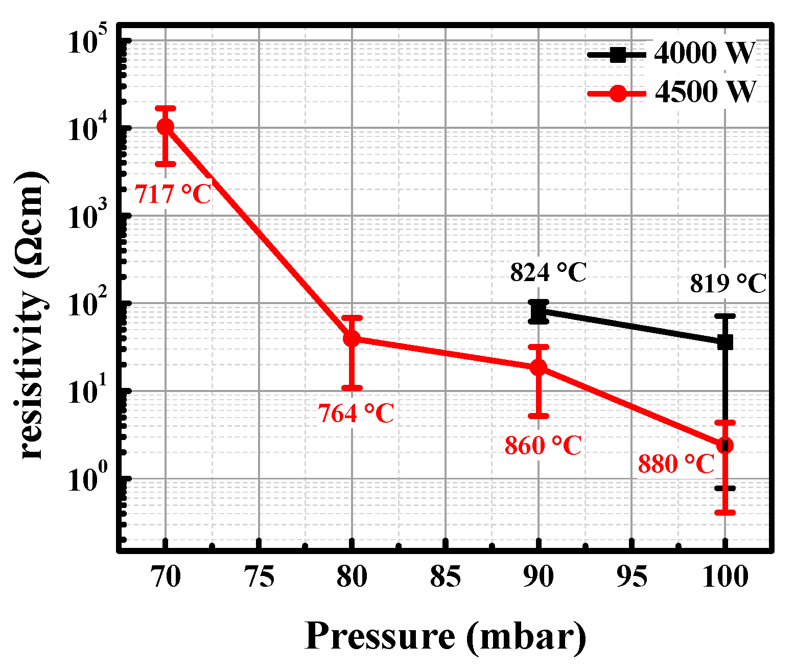
Figure 5 shows the electrical measurements for N-UNCD film grown at 4000 and 4500 W with plasma pressure in the range 70–100 mbar. The electrical conductivity of the N-UNCD films increases (electrical resistivity decreases) as the microwave power and total plasma pressure increases during the films’ growth, obtaining a maximum electrical conductivity (minimum electrical resistivity) for the N-UNCD film grown with a total pressure of 100 mbar and microwave power of 4500 W. This increase in electrical conductivity is correlated with a decrease in the Raman intensities of the TPA bands and an increase in the substrate temperature discussed previously, indicating that N atoms incorporation in the N-UNCD films’ grain boundaries increases with the substrate temperature. Therefore, the effect of increasing the total pressure and microwave power of the plasma during the growth of N-UNCD films results in an increase of the substrate temperature in order to enhance, at the same time, the incorporation of N atoms in the grain boundaries of the N-UNCD films.
The rest of the samples were excessively resistive to be measured. The results shown in
Figure 5 are consistent with data published in the literature, as it has been reported by other authors that a high substrate temperature (>800 °C) is required for more efficient incorporation of N atoms in N-UNCD films [
5,
16,
18].
4. Discussion
Both the pressure and the microwave power applied during the growth of N-UNCD films, using the MPCVD growth process, are critical for the incorporation of N atoms in the N-UNCD film. The gas pressure and microwave power, applied during N-UNCD films growth, influence substantially the temperature of the substrate during film growth, which is critical for efficient N atoms incorporation into the films’ grain boundaries, as shown by the data in
Figure 4 and
Figure 5. The results show that a minimum pressure of 80 mbar is required at a power of 4500 W to obtain a relatively high electrical conductivity in the N-UNCD films. The temperature of the substrate during growth increased, directly proportional to the gas pressure and microwave power, which induce increase of the substrate surface temperature to a maximum value of ~880 °C for the N-UNCD film grown at 100 mbar and 4500 W, correlated to N-UNCD films with the highest electrical conductivity. Thus, the data obtained in the R&D reported here, indicate that 100 mbar and 4500 W provide currently, the optimum parameters combination to produce N-UNCD films with the highest electrical conductivity, until now. The presence of N atoms, in the N-UNCD films was detected using XPS analysis. The XPS spectra showed that the N 1s peak intensity increases, correlating with an increase in electrical conductivity for up to 5 orders of magnitude, compared with the resistivity of insulating UNCD films, indicating that N atoms incorporation in the grain boundaries of UNCD films produces the electrically conductive of the N-UNCD films [
5,
6]. The development of optimized corrosion resistant/electrically conductive N-UNCD films may provide a key application as Lithium (Li)-corrosion resistant coating on anodes and cathodes for Li-ion batteries (LIBs). The N-UNCD coating on the LIBs’ electrodes would protect them from corrosion by Li ions, which are substantially responsible for the degradation of the specific energy after charge/discharge cycles of LIBs. In fact, preliminary experiments performed recently by Auciello and colleagues, demonstrated that LIBs with commercial natural graphite (NG)/copper anodes coated with unoptimized N-UNCD films, exhibit practically no degradation in specific energy after about 100 charge/discharge cycles [
19,
20]. On the contrary, commercial LIBs with uncoated NG/Cu anodes exhibit substantial reduction in specific energy after the same 100 charge/discharge cycles [
19,
20]. In addition, the same preliminary work demonstrated that the N-UNCD coating can eliminate the uncontrollable development of the solid electrolyte interface dendritic layer (known as SEI layer) [
19] at the anode/electrolyte interface. The SEI layer is largely responsible for the degradation in capacitive energy of LIBs [
21] and also is the main contributor to anode overheating and potential subsequent explosive failure [
21], as it occurred in a LIB powering a Samsung cell phone in a plane in 2016, resulting in a billion US dollar loss. Therefore, development of optimized N-UNCD coating may have a transformational positive impact in the development of a new generation of LIBs with ≥10 longer charge/discharge life and order of magnitude safer.
5. Conclusions
The research described in this paper has shown key outcomes critical to the development of unique electrically conductive N-UNCD films to enable a new generation of transformational electrodes for a new generation of Li-ion batteries with orders of magnitude superior stable capacitive energy vs. charge/discharge cycles and safer than current commercial LIBs. Key results from the research are: (1) XRD analysis demonstrated that N-UNCD films are formed by grains with diamond crystalline structure without any graphite impurity phase; (2) Cross-section SEM imaging of N-UNCD films showed that the film thickness decreases as a function of growth pressure, which can correlate with a reduction in arrival of C2 dimers and CHx radical-growth species at the substrate surface, due to collision with other molecules and atoms in the plasma, and reduction in plasma area; (3) XPS analysis revealed the presence of C 1s peak characteristic of diamond, correlating with the XRD data, and the presence of the N 1s peak, indicating the presence of N atoms in the films; (4) Raman analysis revealed a characteristic G band (1550 cm−1) peak, attributed to sp2 carbon bonds, and a D band (1350 cm−1 ) peak attributed to disorder-induced sp2 carbon bonds in grain boundaries; in addition, bands at 1450 cm−1 and 1130 cm−1, correspond to C=C and C-H bonds in transpoliacetilene (TPA) molecules, respectively, The intensity of the TPA peaks (1130 and 1450 cm−1 ), in the Raman spectra of the N-UNCD films, decreased as the total pressure and microwave power increased during film growth, indicating that the grain boundary chemistry of the N-UNCD films presents more sp2 bonded carbon atoms and less TPA bonds, with increasing total pressure and microwave power, resulting from higher incorporation of N atoms, in the grain boundaries, inducing C-N atoms bonding comping with TPA molecular bonds; (5) the electrical conductivity of the N-UNCD films increases as the microwave power and total plasma pressure increases, during the films’ growth, resulting in a maximum electrical conductivity for the N-UNCD film grown with a total pressure of 100 mbar and microwave power of 4500 W, due to N atoms increased incorporation in the N-UNCD films’ grain boundaries, leading to increased electron release upon C-N atoms chemical reactions. It is considered that a better conductivity could occur when the pressure increases more, as long as the deposition rate does not decrease; however, the source that we use for this experiment is limited to a value of 100 mbar and 4500 W, so that right now we are looking for a most powerful source to be able to demonstrate this.


 ,
, 


