Article

A Metal-Insulator-Metal Deep Subwavelength Cavity Based on Cutoff Frequency Modulation

Department of Physics, Chung-Ang University, Seoul 06974, Korea
*
Author to whom correspondence should be addressed.
Submission received: 16 November 2016 / Revised: 23 December 2016 / Accepted: 10 January 2017 / Published: 17 January 2017
(This article belongs to the Special Issue Guided-Wave Optics)

Abstract

:
We propose a plasmonic cavity using the cutoff frequency of a metal-insulator-metal (MIM) first-order waveguide mode, which has a deep subwavelength physical size of 240 × 210 × 10 (nm3) = 0.00013 λ03. The cutoff frequency is a unique property of the first-order waveguide mode and provides an effective mode gap mirror. The cutoff frequency has strong dependence on a variety of parameters including the waveguide width, insulator thickness, and insulator index. We suggest new plasmon cavities using three types of cutoff frequency modulations. The light can be confined in the cavity photonically, which is based on the spatial change of the cutoff frequency. Furthermore, we analyze cavity loss by investigating the metallic absorption, radiation, and waveguide coupling loss; the radiation loss of the higher-order cavity mode can be suppressed by multipole cancellation.

Graphical Abstract

1. Introduction

Surface plasmon polaritons (SPPs), electron oscillations upon coupling with photons, appear at dielectric-metal interfaces by coupling with photons [1]. Recently, many researchers have investigated the miniaturization of photonic devices by using SPPs because of their ability to manipulate photons in subwavelength-sized cavities and waveguides beyond the diffraction limit, which is a fundamental size limit of dielectric photonic devices [2,3,4,5]. In particular, plasmon cavities are exploited in deep subwavelength volume lasers [4,6], switches [7,8], index sensors [9,10], and plasmonic optical filters [11,12,13].
Metal-insulator-metal waveguides can strongly confine SPPs in thin insulators (even in several nanometer-scale dielectric gaps [14,15,16]), where it has been reported that visible light is confined in an ultrasmall dielectric layer. For this reason, MIM waveguide–based cavities were proposed to realize compact devices with various structures, such as disks [17,18], rings [19,20], and blocks [21,22,23]. As the dielectric layer between metals becomes thinner, the propagating SPP mode has a larger k (wavevector), thereby miniaturizing the physical size of the photonic device [13,21,24]. In MIM-based devices, there are two main optical losses: the metal absorption loss and the radiation loss. Although suppression of the absorption loss has been widely studied by introducing high-index dielectric layers inside of low-index dielectric layers [25], radiation loss into free space has not been investigated, despite the fact that it represents a large portion of the total loss.
In this study, we propose MIM cavities made by using a cutoff frequency mechanism that only appears in the dispersion relation of the first-order waveguide mode [13]. The cutoff frequency is strongly dependent on the effective size of the waveguide mode and, therefore, it can be modulated by varying the waveguide width, dielectric thickness, and index of the dielectric. We investigated the optical properties of cavities consisting of two mirror waveguides and a sandwiched waveguide by modulating the cutoff frequency with three different techniques.
The mode gap, which is due to the cutoff frequency difference, prevents radiation loss along the waveguide direction. Alternatively, the higher-order cavity mode observed in a longer cavity has more intensity nodes than the fundamental cavity mode, thereby suppressing radiation loss in the direction orthogonal to the waveguide by multipole cancellation [26].

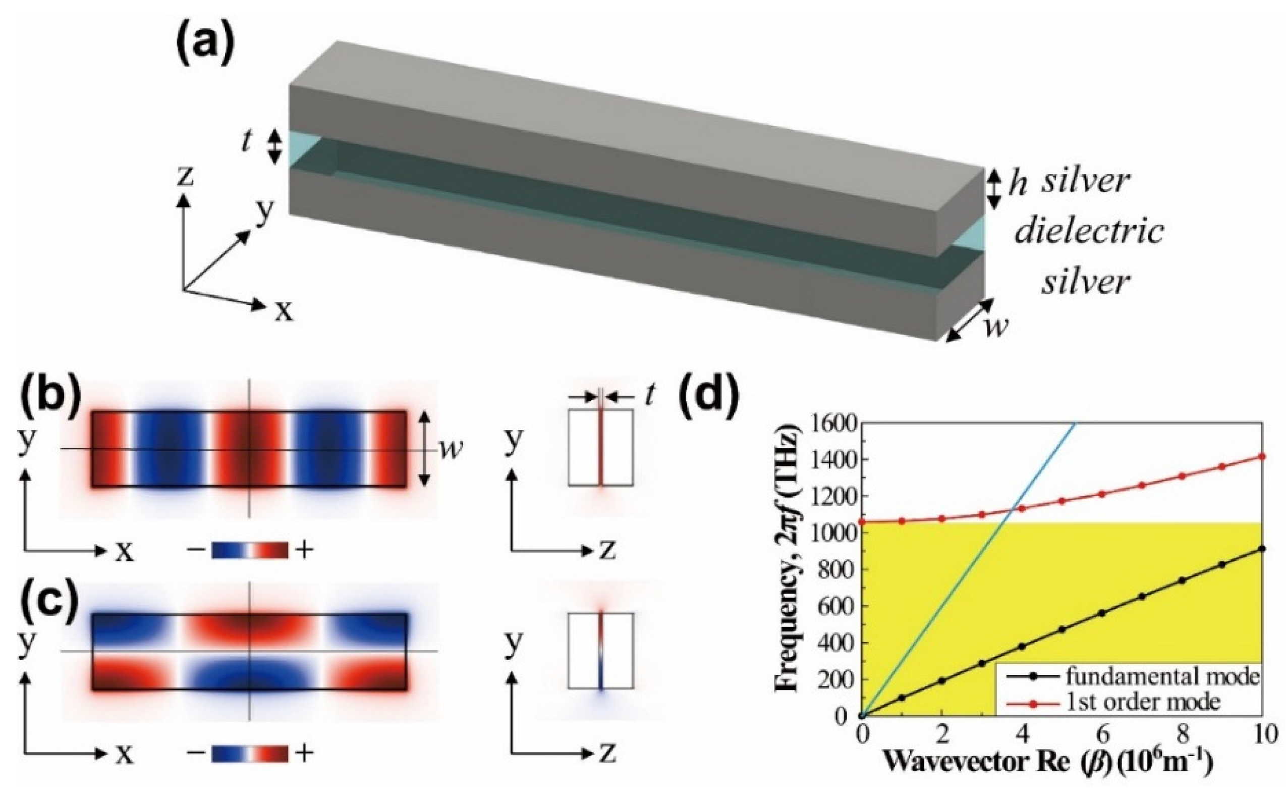
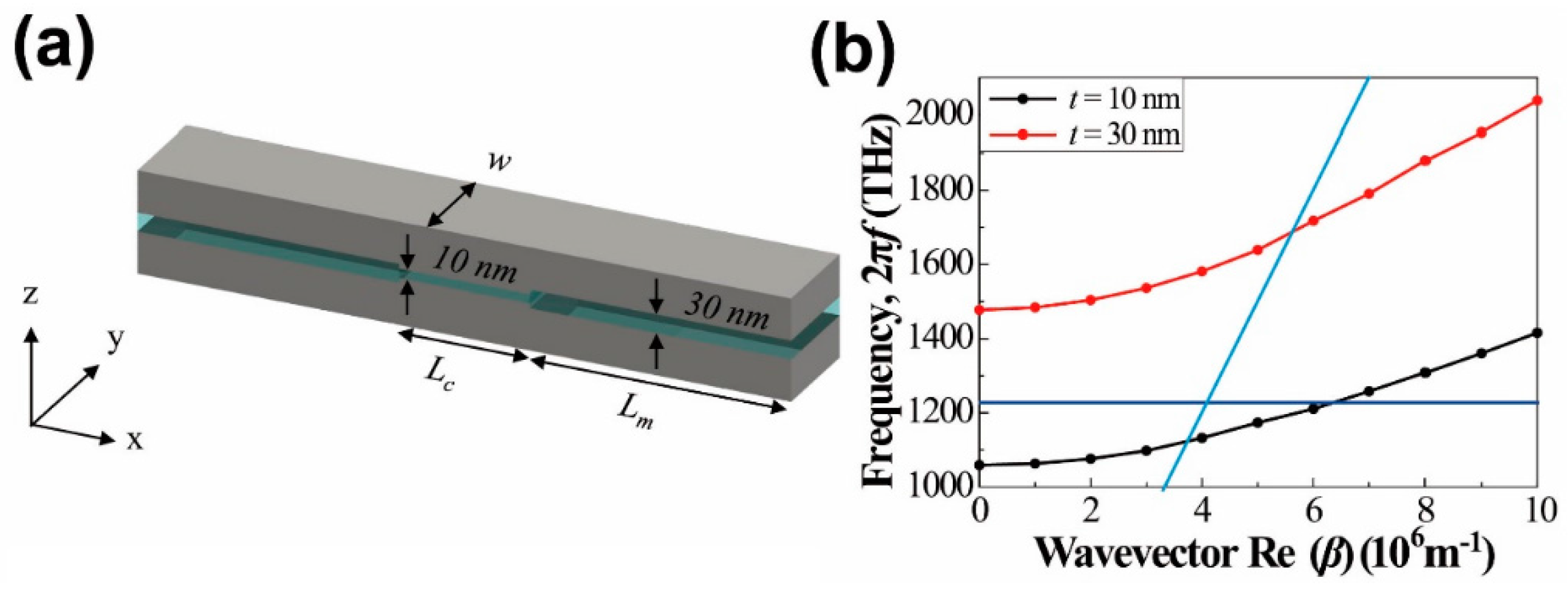
2. Dispersion Properties and Cutoff Frequency

Figure 1a shows a schematic diagram of a MIM waveguide consisting of two silver strips with a sandwiched low-index dielectric layer. Each strip has a thickness (h) of 100 nm and a width (w) of 240 nm. The dielectric layer has a thickness (t) of 10 nm. The refractive index of the dielectric layer is set to 1.5. In this MIM waveguide, the waveguide modes can be classified into fundamental and first-order waveguide modes according to the mirror symmetry of the dominant electric field (Ez) profiles for the plane with y = 0 (dotted lines of Figure 1b,c). Figure 1b,c show the top and side views for the Ez profiles of the fundamental and first-order waveguide modes, respectively, with a wavelength of 1550 nm (λ0). In both modes, the electric fields of the waveguide modes are strongly localized in the deep subwavelength cross-section of the dielectric layer, 240 (w) × 10 (t) (nm2) = 0.00099 (λ02), by index guiding in the y-direction and plasmonic coupling between the silver strips.
Fundamental and first-order MIM waveguide modes have distinct dispersion properties, as shown in Figure 1d. The dispersion curve of the fundamental waveguide mode (black) shows a linear dependence between the frequency and the wavevector. The frequency linearly increases from the zero frequency as the wavevector increases. Alternatively, the dispersion curve of the first-order waveguide mode (red) has a nonzero lowest frequency at the zero wavevector; this is referred to as the cutoff frequency. Below the cutoff frequency, the first-order waveguide mode cannot exist in this MIM waveguide. Thus, the waveguide operates as a mirror for the first-order waveguide mode at frequencies below the cutoff frequency. The frequency region can be considered to be the mode gap of the first-order waveguide mode, which is indicated by the yellow box in Figure 1d. Therefore, the cutoff frequency mechanism can be used to make an effective mirror in the MIM-based cavity.
The cutoff frequency strongly depends on the waveguide width (w) as well as the thickness (t) and refractive index (n) of the dielectric material. This is the case because the effective index of the first-order waveguide mode is sensitive to changes in these structural parameters. By spatially modulating the mode gap with these structural parameters, a photonic well can be formed for the first-order waveguide mode, localizing photons inside of the well. In this paper, we propose three types of deep subwavelength-sized cavities using the difference in cutoff frequency in the first-order waveguide mode.

3. Results

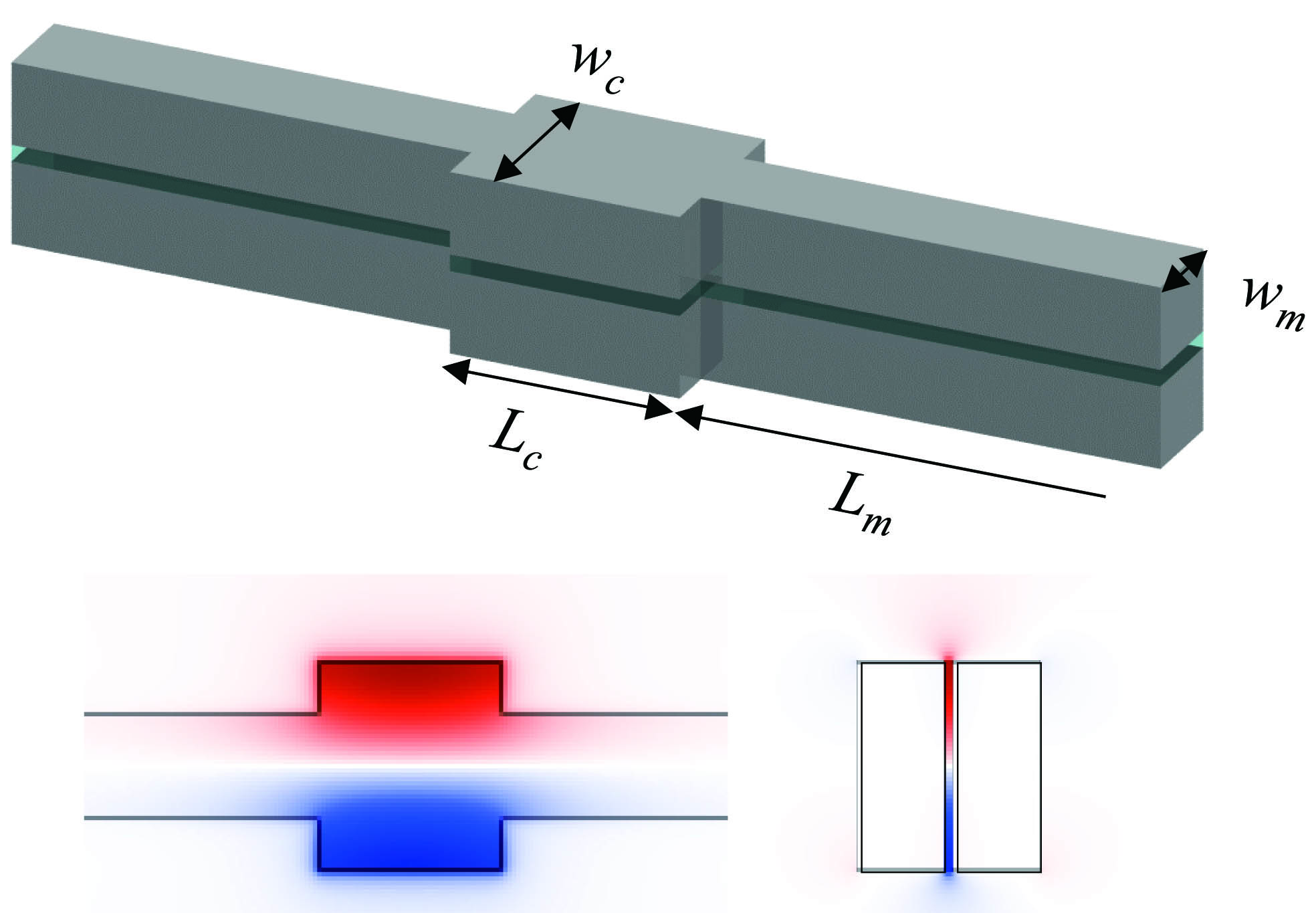
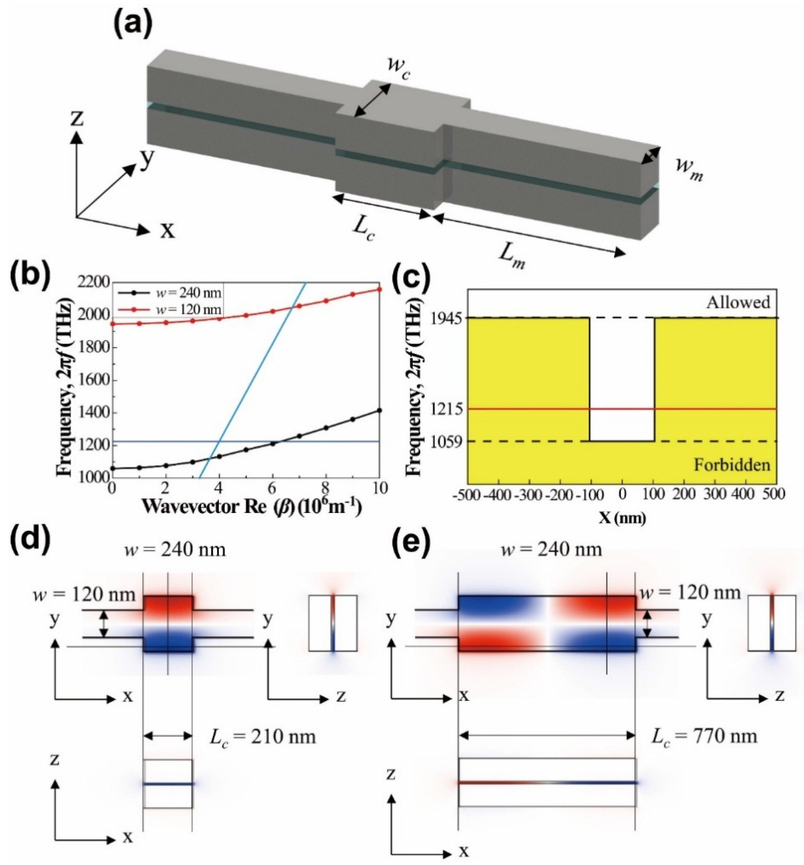
3.1. Waveguide Width-Modulated Cavity

In this paragraph we introduce a MIM first-order mode cavity with width modulation by using the strong width-dependence of the cutoff frequency. Figure 2a shows a schematic of a cavity consisting of a broad waveguide (w = 240 nm) and two narrow mirror waveguides (w = 120 nm), where the waveguides consist of two silver strips and a low-index (n = 1.5) dielectric layer (t = 10 nm). Here, the mirror waveguide length (Lm) is set to 1000 nm.
The dispersion curves of the first-order waveguide modes for broad (w = 240 nm, black) and narrow (w = 120 nm, red) waveguides are plotted in Figure 2b. Since the first-order mode in the narrower waveguide experienced more air outside of the MIM waveguide, the dispersion curve moves upward due to the smaller effective index. In particular, the cutoff frequencies (cutoff wavelength) of the broad/narrow waveguides are 2πf = 1059 THz (1779 nm) and 1945 THz (968 nm), respectively. Propagation of first-order waveguide modes with a frequency between the two cutoff frequencies is allowed for the broad waveguide (w = 240 nm); however, this is forbidden for the narrow waveguide (w = 120 nm). For example, light with a wavelength of 1550 nm (1215 THz), indicated by the horizontal blue line in Figure 2b, is only allowed in the broad waveguide region of Figure 2a. Indeed, the cavity formed a photonic well by modulating the cutoff frequency with the waveguide width, as shown in Figure 2c. The allowed frequency region from 1059 THz (1779 nm) to 1945 THz (968 nm) was localized in the broad waveguide with a length of Lc.
The resonant wavelength of the cavity mode can be controlled by changing the length (Lc) of the cavity region. In addition, the cavity mode is classified as a fundamental and higher-order cavity mode, depending on the number of intensity nodes along the y-direction. Figure 2d,e show the electric field profiles of the fundamental and second-order cavity modes with the same resonant wavelengths (1552 nm) where the dominant electric field is orthogonal to the two metal surfaces. Because both modes are based on the first-order waveguide mode, there is a common intensity node along the x-axis. However, the fundamental cavity mode in the short cavity (Lc = 210 nm) has one intensity antinode along the y-direction. Alternatively, in the long cavity (Lc = 770 nm), the second-order cavity mode has two intensity antinodes along the y-direction.

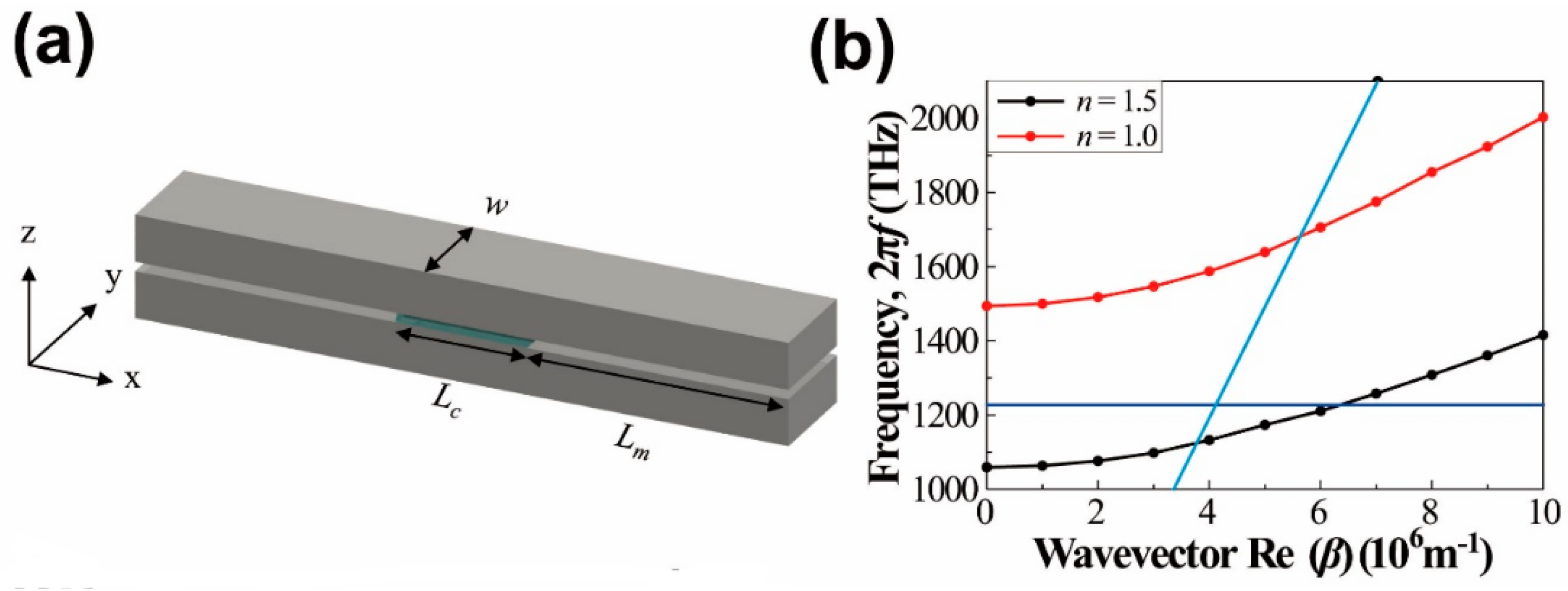
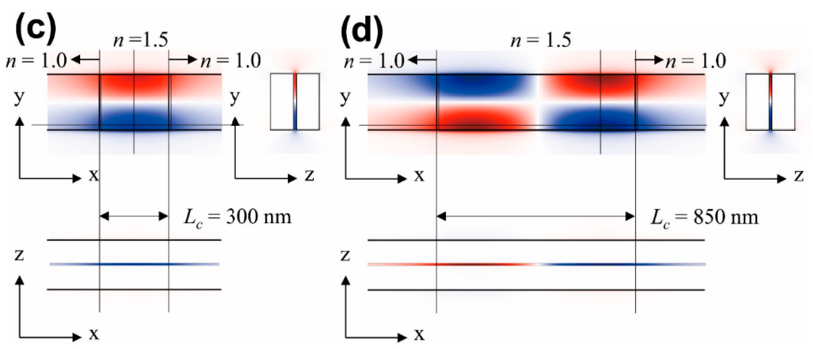
3.2. Refractive Index-Modulated Cavity

The effective waveguide width increases for dielectric materials (between the silver strips) with higher indices, increasing the cutoff frequency of the first-order waveguide mode. Therefore, a first-order mode cavity can be formed by introducing index modulation, as shown in Figure 3a. The cavity consisted of a cavity region with a low-index dielectric layer (n = 1.5) and two mirror waveguides with an air gap (n = 1.0). The waveguide width of 240 nm was kept constant. Here, the height (h) of the silver strips, the distance (t) of the silver strips, and the mirror waveguide length (Lm) were set to 100 nm, 10 nm, and 1000 nm, respectively. Figure 3b shows the dispersion curves of the first-order waveguide modes for dielectric materials with different refractive indices of n = 1.5 (black) and n = 1.0 (red). The cutoff frequency increased from 1059 THz (1779 nm) to 1493 THz (1261 nm) when the dielectric index decreased from 1.5 to 1.0. A photonic well, such as the one shown in Figure 2c, can be generated by the difference in cutoff frequencies at the boundaries, where the refractive index of the dielectric layer changes.
Figure 3c,d show the electric field profiles of the fundamental and second-order cavity modes for resonance wavelengths of 1554 nm and 1550 nm for Lc = 300 nm and Lc = 850 nm, respectively. The mode shapes are similar to those of the width-modulated cavity (Figure 2d,e).

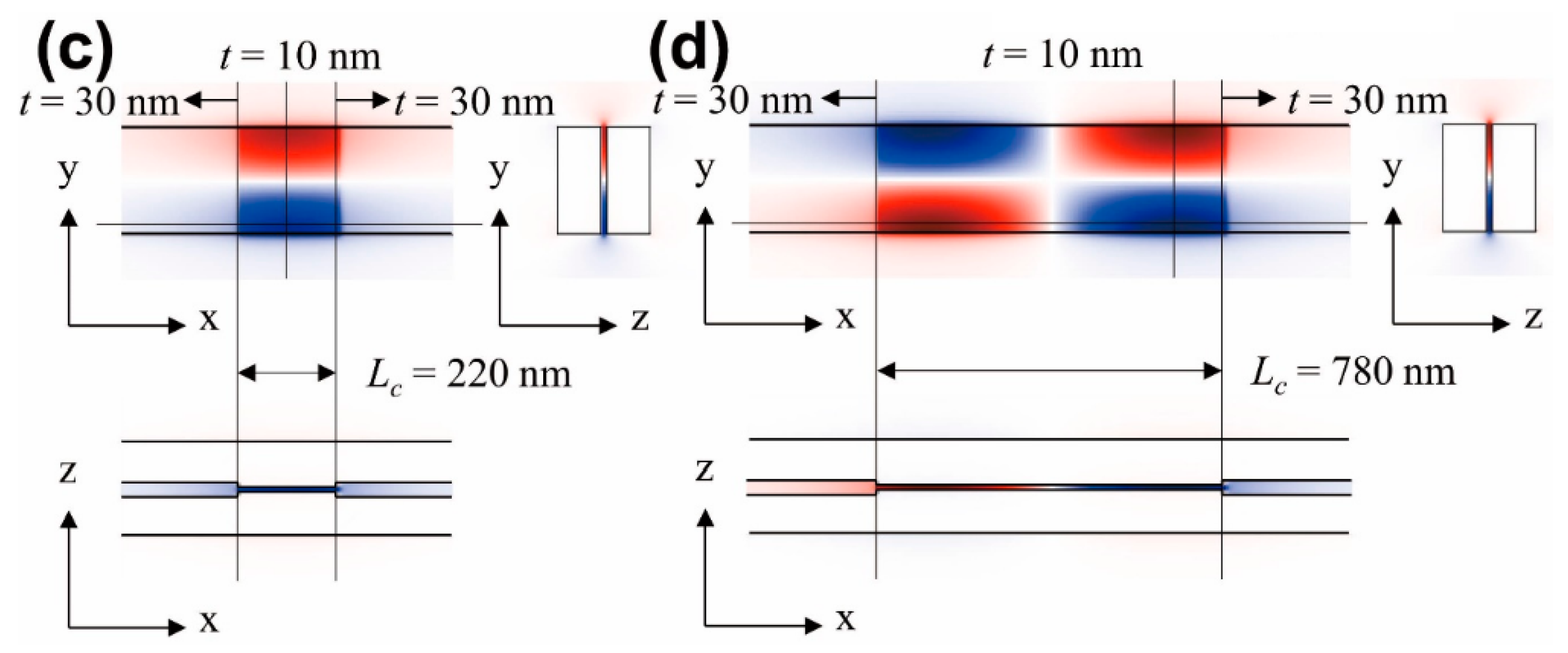
3.3. Gap Size-Modulated Cavity

In the MIM waveguide, the effective index of the waveguide mode increased for thinner dielectric layers between the metal layers [24]. Therefore, as the thickness (t) of the dielectric layer increased, the dispersion curve moved upward due to the smaller effective index (caused by weaker plasmonic coupling). Indeed, the cutoff frequency increased from 1059 THz (1779 nm) to 1945 THz (1414 nm), as shown in the dispersion curves of Figure 4b for t = 10 nm (black) and t = 30 nm (red). Here, the waveguide width (w) and mirror length (Lm) were 240 nm and 1000 nm, respectively. The heights of the cavity and mirror waveguide silver strips were 100 nm and 80 nm, respectively. Because the height of the silver was much larger than the skin depth, changes in the height did not affect the properties of the cavity. Figure 4a shows the schematic of a cavity consisting of a cavity waveguide (t = 10 nm) and two mirror waveguides (t = 30 nm), where the thickness of the dielectric layer was modulated from 10 nm to 30 nm.
Similarly to the waveguide width- or dielectric index-modulated cavities (Figure 2 and Figure 3, respectively), in the dielectric thickness-modulated cavities, the fundamental and second-order cavity modes were observed for Lc = 220 nm (Figure 4c) and Lc = 780 nm (Figure 4d), respectively. Based on the cutoff frequency mirror modulation (similar to the width-modulated cavity (Figure 2) and the index-modulated cavity (Figure 4)), the fundamental and second-order cavity modes were observed at Lc = 220 nm (Figure 4c) and Lc = 780 nm (Figure 4d), respectively.

3.4. Loss Analysis for the Three Cavities

To understand the loss mechanisms of the MIM cavity modes, we investigated each type of loss (i.e., radiation loss, mirror loss, and metallic absorption loss) separately in terms of the quality (Q) factors. The Q factor is defined by 2πf × (stored energy in the cavity/power loss) [13]. The radiation loss corresponds to radiation from the cavity’s sides to free space due to the imperfect horizontal modal confinement of index-guiding. Mirror loss originates from energy loss tunneling through the cutoff frequency mirrors of the narrow waveguides, which have a finite length. In addition, metallic absorption loss results from intrinsic ohmic loss in the silver strips. We were able to obtain Qtot, Qrad, Qm, and Qabs by directly calculating the respective losses because the Q factors were inversely proportional to each loss, the total cavity loss, radiation loss, mirror loss, and absorption loss.
We calculated each Q factor as follows. Qtotal was obtained from the time decay of the total energy in the cavity. Qabs could be obtained by directly calculating the absorbed energy in the metal. Next, we calculated Qoptical with the equation: 1 / Q total = 1 / Q optical + 1 / Q abs . Radiation loss and mirror loss, which consists of the total optical loss, were estimated by calculating the sums of Poynting vectors into free space and through two mirror waveguides, respectively. Qrad and Qm were obtained by the ratio of the sums of Poynting vectors and the following equation, 1 / Q optical = 1 / Q rad + 1 / Q m .
Table 1 shows the Q factors of the three cavities. The Q factors for the three different cutoff frequency-modulated cavities (i.e., width-/index-/gap-modulated cavities) were similar and showed only slight differences. Therefore, by analyzing one of the three cavities, the loss properties of all three cavities could be understood. For example, in the case of a width-modulated cavity, the total Q factors (Qtotal) of the fundamental and the second-order cavity modes were 45.5 and 63.2, respectively. Qm, which is inversely proportional to the mirror loss, was three orders of magnitude larger than the other Q factors when Lm = 1000 nm; therefore, tunneling loss through the cutoff frequency mirror was negligible. Qabs, which is related to the absorption loss (i.e., the dominant loss of the cavities), was between 80 and 90, regardless of the fundamental/second-order cavity modes of the cavities. Additionally, the radiation loss was comparable with the absorption loss. For example, Qrad of the width-modulated cavity was 101 for the fundamental cavity mode and 260 for the second-order cavity mode. Since radiation into free space is difficult to collect (because of its large divergence from 10 nanometer-scale light confinement), it is desirable to minimize this type of loss for practical application of the proposed MIM cavity. Because radiation from the two oppositely-phased Ez intensity antinodes of the second-order mode along the intensity node direction into free space was strongly suppressed by multipole cancellation [26], Qrad of the second-order cavity mode became larger than that of the fundamental cavity mode, increasing Qtotal. On the other hand, the calculated propagation length was 4.8 μm and the reported value was ~5 μm in a similar MIM waveguide [14], which is at least an order of magnitude larger than the proposed cavity size.

5. Conclusions

In summary, we proposed new plasmonic cavities based on modulating the cutoff frequency of MIM first-order waveguide modes. The first-order waveguide mode has a cutoff frequency that depends on the waveguide width, refractive index, and gap size of the dielectric layer. Light (with a wavelength of 1550 nm) can be confined in a cavity region with a deep subwavelength physical volume (0.00013 λ03~0.00055 λ03) in cavities that are modulated by changing the width, index, and gap size. The second-order cavity mode shows higher Q factors than the fundamental cavity mode because radiation along the intensity node is suppressed by multipole cancellation.
The proposed ultrasmall cavity is a good candidate for low-threshold lasers [27], ultrafast optical switches [28], and as the light source for quantum optics [6] due to its extremely small mode size of 1/10,000 λ03. In addition, its waveguide-based design allows for efficient light coupling with integrated detectors [29] or other photonic devices [8,30,31,32]. The light coupling can be achieved by using a tapered coupler from a dielectric waveguide [33] or a dielectric air slot waveguide [34]. The cutoff frequency mechanism can be widely applied to build efficient and strong mirror waveguides for various optical components operating at any wavelengths. Since the mirrors of the proposed cavity have adjustable reflectivity, unidirectional emission can be easily achievable. Usually, although the control of directionality is highly demanded for an efficient light source in quantum optics and photonic circuits, it is extremely difficult to control the directionality in the deep subwavelength cavity. The cavity mode can be directly excited by the odd waveguide mode from the dielectric waveguide with an external light source or internal light emitter such as quantum dots. The continuation of this study will involve modulating the nanocavity width, dielectric index, dielectric thickness, and structure to miniaturize key optical devices into deep subwavelength-scaled ones in integrated devices and nano-emitters.

Acknowledgments

This research was supported in part by the National Research Foundation of Korea (NRF) grant funded by the Korean government (MSIP) (No. NRF-2016R1C1B2007007) and in part by the Chung-Ang University Research Scholarship Grants in 2016.

Author Contributions

Soon-Hong Kwon conceived and designed the whole simulation and concept; Kihwan Moon and Tae-Woo Lee performed the simulations and analyzed the data; Soon-Hong Kwon, Kihwan Moon, and Young Jin Lee drafted and revised the manuscript.

Conflicts of Interest

The authors declare no conflicts of interest.

References

  1. Barnes, W.L.; Dereux, A.; Ebbesen, T.W. Suface plasmon subwavelength optics. Nature 2003, 424, 824–830. [Google Scholar] [CrossRef] [PubMed]
  2. Gramotnev, D.K.; Bozhevolnyi, S.I. Plasmonics beyond the diffraction limit. Nat. Photonics 2010, 4, 83–91. [Google Scholar] [CrossRef]
  3. Wei, H.; Li, Z.P.; Tian, X.R.; Wang, Z.X.; Cong, F.Z.; Liu, N.; Zhang, S.P.; Nordlander, P.; Halas, N.J.; Xu, H.X. Quantum dot-based local field imaging reveals plasmon-based interferometric logic in silver nanowire networks. Nano Lett. 2010, 11, 471–475. [Google Scholar] [CrossRef] [PubMed]
  4. Ma, R.M.; Oulton, R.F.; Sorger, V.J.; Bartal, G.; Zhang, X. Room-temperature sub-diffraction-limited plasmon laser by total internal reflection. Nat. Mater. 2011, 10, 110–113. [Google Scholar] [CrossRef] [PubMed]
  5. Zhang, S.P.; Xu, H.X. Optimizing substrate-mediated plasmon coupling toward high-performance plasmonic nanowire waveguides. ACS Nano 2012, 6, 8128–8135. [Google Scholar] [CrossRef] [PubMed]
  6. Oulton, R.F.; Sorger, V.J.; Zentgraf, T.; Ma, R.M. Plasmon lasers at deep subwavelength scale. Nature 2009, 461, 629–632. [Google Scholar] [CrossRef] [PubMed]
  7. Nikolajsen, T.; Leosson, K.; Bozhevolnyi, S.I. Surface plasmon based modulators and switches operating at telecom wavelengths. Appl. Phys. Lett. 2004, 85, 5833–5835. [Google Scholar] [CrossRef]
  8. Fang, Y.R.; Li, Z.P.; Huang, Y.Z.; Zhang, S.P.; Nordlander, P.; Halas, N.J.; Xu, H.X. Branched silver nanowires as controllable plasmon routers. Nano Lett. 2010, 10, 1950–1954. [Google Scholar] [CrossRef] [PubMed]
  9. Tsai, C.Y.; Lu, S.P.; Lin, J.W.; Lee, P.T. High sensitivity plasmonic index sensor using slablike gold nanoring arrays. Appl. Phys. Lett. 2011, 98, 153108. [Google Scholar] [CrossRef] [PubMed]
  10. Kwon, S.H. Deep subwavelength-scale metal-insulator-metal plasmonic disk cavities for refractive index sensor. IEEE Photonics J. 2013, 5, 4800107. [Google Scholar] [CrossRef]
  11. Volkov, V.S.; Bozhevolnyi, S.I.; Devaux, E.; Laluet, J.Y.; Ebbesen, T.W. Wavelength selective nanophotonic components utilizing channel plasmon polaritons. Nano Lett. 2007, 7, 880–884. [Google Scholar] [CrossRef] [PubMed]
  12. Rahimzadegan, A.; Granpayyeh, N.; Hosseini, S.P. Improved plasmonic filter, ultra-compact demultiplexer, and splitter. J. Opt. Soc. Korea 2014, 18, 261–273. [Google Scholar] [CrossRef]
  13. Lee, T.W.; Lee, D.E.; Kwon, S.H. Dual-function metal-insulator-metal plasmonic opticla filter. IEEE Photonics J. 2015, 7, 4800108. [Google Scholar] [CrossRef]
  14. Veronis, G.; Fan, S.H. Modes of subwavelength plasmonic slot waveguides. J. Lightwave Technol. 2007, 25, 2511–2521. [Google Scholar] [CrossRef]
  15. Pile, D.F.P.; Ogawa, T.; Gramotnev, D.K.; Matsuzaki, Y.; Vernon, K.C.; Yamaguchi, K.; Okamoto, T.; Haraguchi, M.; Fukui, M. Two-dimensionally localized modes of a nanscale gap plasmon waveguide. Appl. Phys. Lett. 2005, 87, 261114. [Google Scholar] [CrossRef] [Green Version]
  16. Tagliabue, G.; Poulikakos, D.; Eghlidi, H. Three-dimensional concentration of light in deeply sub-wavelength, laterally tapered gap-plasmon nanocavities. Appl. Phys. Lett. 2016, 108, 221108. [Google Scholar] [CrossRef]
  17. Kuttge, M.; de Abajo, F.J.G.; Polman, A. Ultasnall mode volume plasmonic nanodisk trsonators. Nano Lett. 2010, 10, 1537–1541. [Google Scholar] [CrossRef] [PubMed]
  18. Kwon, S.H. Deep subwavelength plasmonic whispering-gallery-mode cavity. Opt. Express 2012, 20, 24918–24924. [Google Scholar] [CrossRef] [PubMed]
  19. Han, Z.H.; Bozhevolnyi, S.I. Plasmon-induced transparency with detuned ultracompact Fabry-Perot resonators in integrated plasmonic devices. Opt. Express 2011, 19, 3251–3257. [Google Scholar] [CrossRef] [PubMed]
  20. Zand, I.; Abrichamian, M.S.; Berini, P. Highly tunable nanoscale metal-insulator-metal split ring core ring resonators (SRCRRs). Opt. Express 2013, 21, 79–86. [Google Scholar] [CrossRef] [PubMed]
  21. Kwon, S.H. Plasmonic ruler with angstrom distance resolution based on double metal block. IEEE Photonics Technol. Lett. 2013, 25, 1619–1622. [Google Scholar] [CrossRef]
  22. Lassiter, J.B.; McGuire, F.; Mock, J.J.; Ciralci, C.; Hill, R.T.; Wiley, B.J.; Chilkoti, A.; Smith, D.R. Plasmonic waveguide modes of film-coupled metallic nanocubes. Nano Lett. 2013, 13, 5866–5872. [Google Scholar] [CrossRef] [PubMed]
  23. Nielsen, M.G.; Gramotnev, D.K.; Pors, A.; Albrektsen, O.; Bozhevolnyi, S.I. Continuous layer gap plasmon resonators. Opt. Express 2011, 19, 19310–19322. [Google Scholar] [CrossRef] [PubMed]
  24. Miyazaki, H.T.; Kurokawa, Y. Contolled plasmon resonance in closed metal/insulator/metal nanocavities. Appl. Phys. Lett. 2006, 89, 211126. [Google Scholar] [CrossRef]
  25. Oulton, R.F.; Sorger, V.J.; Genov, D.A.; Pile, D.F.P.; Zhang, X. A hybrid plasmonic waveguide for subwavelength confinement and long-range propagation. Nat. Photonics 2008, 2, 496–500. [Google Scholar] [CrossRef]
  26. Johnson, S.G.; Fan, S.; Mekis, A.; Joannopoulos, J.D. Multipole-cancellation mechanism for high-Q cavities in the absence of a complete photonic and gap. Appl. Phys. Lett. 2001, 78, 3388–3390. [Google Scholar] [CrossRef]
  27. Hill, M.T.; Oei, Y.S.; Smalbrugge, B.; Zhu, Y.; De Vries, T.; Van Veldhoven, P.J.; Van Otten, F.W.M.; Eijkemans, T.J.; Turkiewicz, J.P.; De Waardt, H.; et al. Lasing in metallic-coated nanocavities. Nat. Photonics 2007, 1, 589–594. [Google Scholar] [CrossRef]
  28. Lu, H.; Liu, X.M.; Wang, L.R.; Gong, Y.K.; Mao, D. Ultrafast all-optical switching in nanoplasmonic waveguide Kerr nonlinear resonator. Opt. Express 2011, 19, 2910–2915. [Google Scholar] [CrossRef] [PubMed]
  29. Zhu, S.Y.; Lo, G.Q.; Kwong, D.L. Theorical investigation of silicide Schottky barrier detector integrated in horizontal metal-insulator-metal nanoplasmonic slot waveguide. Opt. Express 2011, 19, 15843–15854. [Google Scholar] [CrossRef] [PubMed]
  30. Wang, W.; Yang, Q.; Fan, F.; Xu, H.; Wang, Z.L. Light Propagation in Curved Silver Nanowire Plasmonic Waveguides. Nano Lett. 2011, 11, 1603–1608. [Google Scholar] [CrossRef] [PubMed]
  31. Wei, H.; Xu, H. Nanowire-based plasmonic waveguides and devices for integrated nanophotonic circuits. Nanophotonics 2012, 1, 155–169. [Google Scholar] [CrossRef]
  32. Gramotnev, D.K.; Nielsen, M.G.; Tan, S.J.; Kurth, M.L.; Bozhevolnyi, S.I. Gap surface plasmon waveguides with enhanced integration and functionality. Nano Lett. 2012, 12, 359–363. [Google Scholar] [CrossRef] [PubMed]
  33. Veronis, G.; Fan, S.H. Theoretical investigation of compact couplers between dielectric slab waveguides and two-dimensional metal-dielectric-metal plasmonic waveguides. Opt. Express 2007, 15, 1211–1221. [Google Scholar] [CrossRef] [PubMed]
  34. Zhu, B.Q.; Tsang, H.K. High Coupling Efficiency Silicon Waveguide to Metal-Insulator-Metal Waveguide Mode Converter. J. Lightwave Technol. 2016, 34, 2467–2472. [Google Scholar] [CrossRef]
Figure 1. (a) Schematic of a metal-insulator-metal (MIM) waveguide consisting of two silver strips and a low-index dielectric layer. The variables w, h, and t represent the waveguide width, the thickness of the silver strip, and the thickness of the dielectric layer, respectively; (b,c) Top and side views of the Ez electric field profiles of the fundamental and first-order waveguide modes with a wavelength of 1550 nm, w = 240 nm, h = 100 nm, and t = 10 nm. The top view (left) is obtained in the center of the dielectric layer and the side view (right) is obtained along the solid line of the top view; (d) Dispersion curves of fundamental (black) and first-order (red) waveguide modes, respectively. The yellow box indicates the mode gap region for the odd waveguide mode. Light line is indicated by blue line.
Applsci 07 00086 g001
Figure 2. (a) Schematic of a cavity consisting of a broad waveguide (w = 240 nm) and two narrow mirror waveguides (w = 120 nm). Here, h = 100 nm, t = 10 nm, Lm = 1000 nm, and the cavity length is Lc; (b) Dispersion curves of first-order waveguide modes for waveguide widths of w = 240 nm (black) and w = 120 nm (red); their cutoff frequencies (cutoff wavelengths) are 2πf = 1059 THz (1779 nm) and 1945 THz (968 nm), respectively. The horizontal blue line indicates a frequency (wavelength) of 1215 THz (1550 nm). The light line is indicated by the blue line; (c) Cutoff frequency of the first-order waveguide mode along the x-axis for the cavity in (d). The allowed and forbidden regions are indicated by white and yellow colors, respectively. The allowed frequency region for the first-order waveguide mode is spatially changed by modulating the waveguide width; (d,e) Top and side views of the electric field profiles of the fundamental (Lc = 210 nm) and second-order (Lc = 770 nm) cavity modes, respectively. The solid lines indicate the cross-sections of the side views.
Applsci 07 00086 g002
Figure 3. (a) Schematic of a cavity consisting of a cavity region (n = 1.5, green color) and two mirror waveguides (n = 1.0). Here, w = 240 nm, h = 100 nm, t = 10 nm, Lm = 1000 nm, and the cavity length is Lc; (b) Dispersion curves of first-order waveguide modes for dielectric materials (between the silver strips) with different refractive indices of n = 1.5 (blue) and n = 1.0 (red). The cutoff frequencies (wavelengths) are 2πf = 1059 THz (1779 nm) and 1493 THz (1261 nm), respectively. The horizontal blue line indicates a frequency of 1215 THz (1550 nm). The light line is indicated by the blue line; (c,d) Top and side views of the electric field profiles of fundamental (Lc = 300 nm) and second-order (Lc = 850 nm) cavity modes.
Applsci 07 00086 g003aApplsci 07 00086 g003b
Figure 4. (a) Schematic of a cavity consisting of a cavity waveguide (t = 10 nm) and two mirror waveguides (t = 30 nm). The gap size between the two silver strips is modulated. In the gap, a low-index dielectric layer (n = 1.5) is assumed. Here, w = 240 nm, Lm = 1000 nm, and the heights of the cavity and mirror waveguide silver strips are 100 nm and 80 nm, respectively. The cavity waveguide length is Lc; (b) Dispersion curves of the first-order waveguide modes for t = 10 nm (blue) and t = 30 nm (red). The cutoff frequencies (wavelengths) are 2πf = 1059 THz (1779 nm) and 1945 THz (1414 nm). The light line is indicated by the blue line; (c,d) Top and side views of the electric field profiles of the fundamental (Lc = 220 nm) and second-order (Lc = 780 nm) cavity modes.
Applsci 07 00086 g004aApplsci 07 00086 g004b
Table 1. Quality factors of the three cavities.
Cavity TypeFundamental ModeSecond Order Mode
QtotalQradQabsQmQtotalQradQabsQm
Width-modulated cavity (Figure 2)45.510182.89.05 × 10563.226083.61.81 × 106
Index-modulated cavity (Figure 3)38.671.783.79.68 × 10456.817584.21.71 × 105
Gap-modulated cavity (Figure 4)37.364.089.71.42 × 10456.616486.62.82 × 104

