
Non-Linear Thermoelectric Devices with Surface-Disordered Nanowires


1
Department of Experimental Physics, Faculty of Mathematics, Physics and Informatics, Comenius University in Bratislava, 842 28 Bratislava, Slovakia
2
Department of Physics, University of Florida, Gainesville, FL 32611, USA
*
Author to whom correspondence should be addressed.
Appl. Nano 2021, 2(3), 162-183; https://0-doi-org.brum.beds.ac.uk/10.3390/applnano2030013
Submission received: 24 June 2021
/
Revised: 5 July 2021
/
Accepted: 7 July 2021
/
Published: 12 July 2021
(This article belongs to the Collection Feature Papers for Applied Nano)
Abstract
:We reviewed some recent ideas to improve the efficiency and power output of thermoelectric nano-devices. We focused on two essentially independent aspects: (i) increasing the charge current by taking advantage of an interplay between the material and the thermodynamic parameters, which is only available in the non-linear regime; and (ii) decreasing the heat current by using nanowires with surface disorder, which helps excite localized phonons at random positions that can strongly scatter the propagating phonons carrying the thermal current.
1. Introduction
Thermoelectric devices can convert unused waste heat into electricity or use electricity for refrigeration [1]. The idea is very simple. Suppose the two ends of a wire are kept at two different but fixed temperatures. The hot end with temperature has typically a higher density of more energetic electrons compared to the cold end kept at temperature , so they diffuse from the hot end to the cold end, until charge imbalance stops the flow. This results in a chemical potential of the cold end larger than the chemical potential of the hot end . This difference can be used, e.g., to light a bulb (a ‘load’), as shown in Figure 1.
1.1. Electrical vs. Thermal Current
The efficiency of such a device depends on how much electrical current is generated, given the heat current from the hot reservoir that measures the input energy. A good thermoelectric material needs to have a large electrical conductivity (an “electron metal”) and at the same time, a poor thermal conductivity (a “phonon glass”). While significant progress has been made in recent years in improving thermoelectric figure of merit [2], typical bulk materials with large (good metals) turn out to be inherently inefficient [3,4]. This is because the ratio of the two conductivities at a given temperature, where T is the temperature, is a fixed number (known as the Lorentz number) independent of the material properties given by the Wiedemann–Franz law [5]:
where is the Boltzmann constant and e is the electric charge. As a result, it has not yet been possible to find bulk thermoelectric materials efficient enough to be cost effective except in specialized applications such as space travel. Since the Wiedemann–Franz law is a consequence of the Fermi-liquid theory, attempts have been made to beat the law by looking for non-Fermi-liquid states of matter. While possible in principle [6,7], such exotic states in the bulk are typically not very useful in practical devices. On the other hand, it seems possible to control and independently in nano-engineered low-dimensional materials, boosting the efficiency [8,9,10,11,12,13,14,15,16]. A typical nano-device consists of two large leads at different temperatures connected by a quantum dot [17,18,19,20,21], a molecule [22,23,24,25,26,27], or a nanowire [28,29,30,31,32,33,34]. Naturally, the power output of such a nano-device is also going to be small. In order to be practically useful, an important question is whether such a nano-device can be scaled up to generate a large enough power output.
1.2. Linear Response Regime
In general, the number current across a given thermoelectric material connected to two leads depends on the energy-dependent transmission function of the material:
Here, the function is defined as
where is the Fermi function of the lead , using notations from Figure 1. In the linear response regime where and are assumed to be infinitesimally small, the difference of Fermi-functions can be expanded as
Then, the number current becomes
where is the conductivity and is the Seebeck coefficient. The derivative of the Fermi-function (which, at low temperatures, is nearly a delta-function at where is the Fermi-energy) means that material properties near the Fermi energy, such as the conductivity and the Seebeck coefficient, determine the number current in the linear response regime. In terms of these properties, the effectiveness of a thermoelectric material is usually estimated by its thermoelectric Figure of Merit:
where the thermal conductivity contains contributions from electrons as well as phonons.
Currently, the best available devices have , while it is estimated that would be industrially competitive. Since the Figure of Merit shown by (6) solely depends on the properties of the material connecting the leads, it is natural that most work in this area has been focused on designing (or nano-engineering) a good thermoelectric material, an “electron-metal, phonon-glass”, exploiting complex structures [35,36]. There are also clever ways to increase the efficiency by considering multi-terminal systems [26]. In this review, we will not consider the progress made in these areas. Instead, we will focus on two recent ideas to improve the efficiency and power output of thermoelectric nano-devices: one is to take advantage of the non-linear regime, with a particular focus on being able to tune the device for better efficiency. It turns out that the efficiency depends not only on the material parameters, but also crucially on the thermodynamic parameters of the leads as well as the characteristics of the loads. This opens novel possibilities to improve the efficiency of a thermoelectric device by exploiting the interplay between the material and the thermodynamic parameters of the device. The other idea is to exploit the observation that surface disorder in nanowires favors excitation of resonances and the eventual localization of phonons across the wire when a propagating phonon is introduced. This offers the possibility that the thermal current can be decreased by a significant amount if the heat-carrying propagating phonons become strongly scattered by the localized phonons in such a surface-disordered nanowire.
2. Non-Linear Regime
The linear-response regime is valid when the temperature and the chemical potential difference between the two leads are small. On the other hand, in practically useful systems, the temperature as well as the chemical potential difference between the leads are not necessarily small, and non-linearity becomes important. Several recent work addresses the effects of non-linearity in thermoelectric devices [21,34,37,38,39,40]. We will not review these efforts here. Instead, we will focus on a general framework that allows exploiting the non-linearity to increase the efficiency and power output of a thermoelectric device.
In Figure 1, the device takes heat from the hot reservoir kept at temperature , does work W, and releases heat to the cold reservoir kept at a temperature . The efficiency is defined as the ratio of work done to the heat extracted from the high temperature reservoir:
where the latter follows from the conservation of energy. An ideal engine would have the maximum efficiency, called the Carnot efficiency, defined as
which occurs when the system is reversible. For a typical application, such as using the waste heat from a hot car engine, K and K, which is roughly the room temperature. In this case, . It will be useful to keep this in mind when designing a device for a given application.
The estimate of for industrial competitiveness mentioned above translates to [41]:
The goal is then to design a device with , with some given .
2.1. Power Output and Efficiency
The power output in the general non-linear regime is the product of the charge current times that the voltage drops across the device. In our notation of Figure 1, it is given by
where is the number current defined in (2). In this notation, the efficiency is:
Interestingly, there have been several proposals for devices with Carnot efficiency [42,43,44,45]. However, the power output from such systems is zero, since they are reversible. Such systems are of course useless as practical devices. It is therefore important to simultaneously consider the efficiency and the power output in any proposed device [41,46,47,48]. Whitney [46] has shown that the maximum efficiency for a given power output occurs when the energy dependent transmission through the system is a square wave, with appropriate position and width.
2.2. Interplay of Material and Thermodynamic Parameters
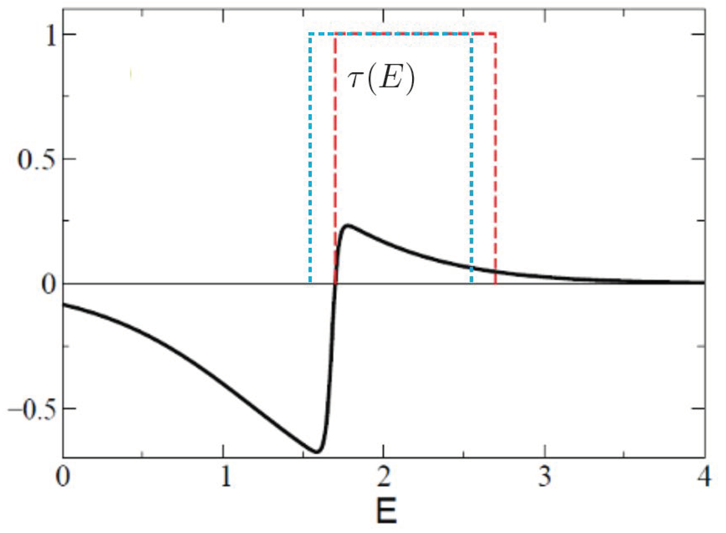
For simplicity, Figure 2 considers an ideal square-wave transmission function as an example. Note that this is a fixed property of a given material. At the same time, Figure 2 shows the general form of , the difference in Fermi functions, which is entirely determined by the thermodynamic parameters of the system. It has a negative and a positive part, the zero of the function being at:
[Note: rewriting as , it is clear that for a given and with , both chemical potentials must lie on the same side of the parameter , satisfying the inequalities (case I) or (case II). For definiteness, and without loss of generality, we will only consider case I].
![Applnano 02 00013 g002]()
Figure 2.
Optimizing transmission function in the nonlinear regime. Difference of the Fermi functions (solid black curve) with , , , and and two identical width square-wave transmission functions , one (blue) starting at energy and a second one (red) starting at [41].
Figure 2.
Optimizing transmission function in the nonlinear regime. Difference of the Fermi functions (solid black curve) with , , , and and two identical width square-wave transmission functions , one (blue) starting at energy and a second one (red) starting at [41].

The general form of and an ideal square-wave transmission function shown in Figure 2 provide valuable insights into the ways to optimize both efficiency and power. It is clear from Figure 2 and Equations (10) and (11) that the efficiency or power output of a thermoelectric device in this non-linear regime does not depend on the material property alone; they also depend very crucially on the position of the crossover energy where changes sign, which is entirely determined by the thermodynamic parameters , , , and . To illustrate the interplay between the material and the thermodynamic parameters, consider two identically shaped transmission functions, shown in red and blue in Figure 2, but with different onset energies , with (blue) and (red). Clearly for , part of the contribution to the integral determining the number current (10) from the positive part of is going to be canceled by the contribution from the negative part of , leading to a small number current, which can be as small as zero—even with an ideal square-wave transmission function (negative values simply mean a current in the opposite direction, so the same argument applies in that case too). On the other hand, for , the contribution to the number current from all energy where is non-zero is going to add up, leading to a much larger number current. Thus, for a given , it is extremely important to be able to tune the parameter (or vice versa), in order to be able to maximize the number current. Together with the facts that (i) Carnot efficiency is necessarily associated with zero power output; and (ii) the power output from any nano-device is going to be too small to be practically useful, the above insight suggests the following design criteria for a good thermoelectric nano-device, irrespective of the material [41]:
- 1.
- It should have a tunable phenomenon leading to a negligible value for in the range of E dictated by ;
- 2.
- Any design has to optimize the power output and the efficiency simultaneously, as opposed to maximizing one or the other;
- 3.
- Any nano-device should be scalable, with the number current increasing with the number of channels.
2.3. Nanowires
The above discussions are valid irrespective of whether the device itself is a quantum dot, a large molecule or a wire. For example, a molecular system known as a t-stub can exploit the interference effects from two possible paths to tune the transmission function [41,49]. On the other hand, given the available technology, it is easy to fabricate nanowires, and for practical purposes, a device based on nanowires seems more desirable. In particular, as we will see later, silicon nanowires with a surface disorder can have very low thermal conductivity, which is a requirement for a good thermoelectric device. Thus, we will focus our review on nanowires only.
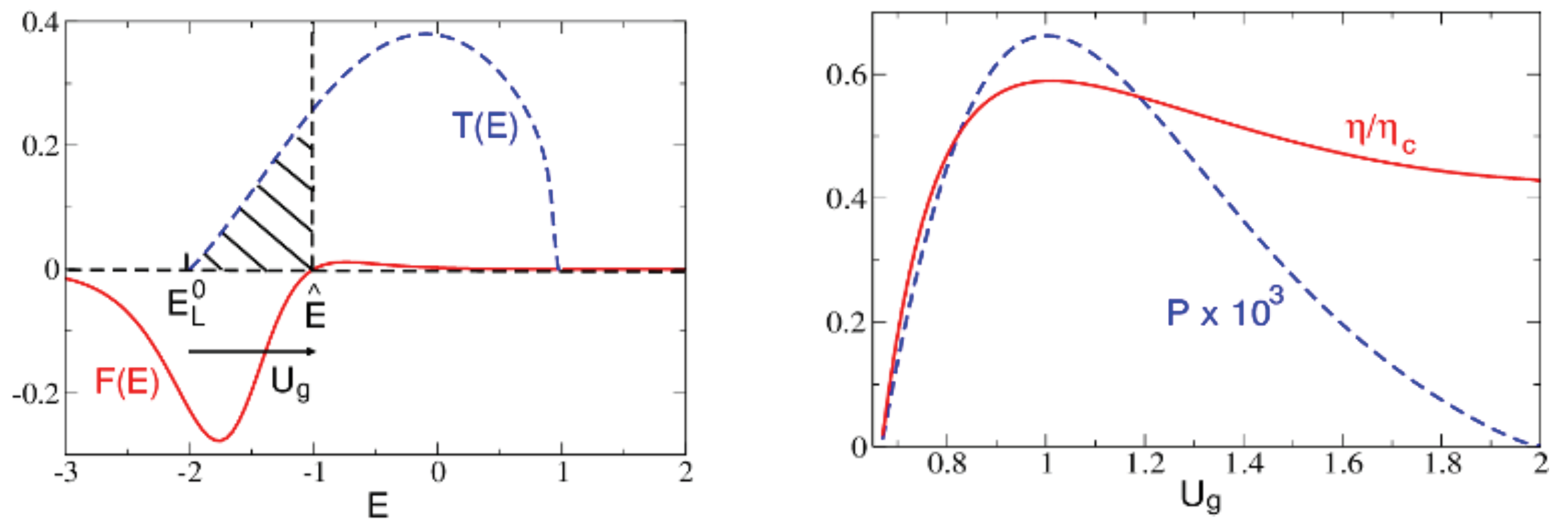
A proposal from Ref. [50] provides a sketch for a tunable thermoelectric device based on nanowires. The proposal assumes that the lower impurity band edge of a semiconducting nanowire can be modified within a reasonable range by applying a gate voltage . Given , only electrons with energy will be in the allowed band, and the resulting transmission function will be zero for all . In the absence of the gate voltage, when the wire is connected to the leads and the load, the lower band edge will, in general, be different from determined by the thermodynamic parameters of the system. By applying a tunable gate voltage, it should now be possible to align precisely, thus maximizing the number current. The tuning allows for optimizing power output and efficiency simultaneously.
Figure 3, reprinted from [50], shows the transmission function of a weakly disordered wire (localization length ten times larger than the length of the wire) obtained from an exactly solvable model of a one-dimensional wire with N sites described by a standard tight-binding model and a Lorentzian disorder:
where t is the hopping element and W is the strength of disorder. All energies are measured in units of the hopping element t. For particular choices of the coupling to the leads, the transmission function is shown in Figure 3, the lower band edge being at . Thermodynamic parameters are chosen for which the function is also shown, with the crossover energy . Application of a gate voltage characterized by the parameter shifts all energies in the transmission function by , so that the new lower band edge is at . The corresponding power and relative efficiency as a function of is shown in the right panel in Figure 3. The increase in efficiency is quite remarkable, given the estimate that can make a device industrially competitive. The power P is not maximum at the same gate voltage where the efficiency is maximum, but there is a range of for which both the efficiency and the power output are large.
While the above estimate is promising, the maximum power P for a single nanowire considered in Figure 3 is of the order . This is clearly too small to be useful in any practical device. However, the advantage here is that one can have a large number of independent parallel wires, all connected to the same leads and all subject to the same gate voltage, which will increase the power output without compromising efficiency. In other words, such a device is scalable. One limiting consideration is that if the wires are too close to each other, then the interactions between them can become important, and the wires can no longer be treated as independent.
One important additional advantage of the tunable device is that in any device, the chemical potential will depend on the resistance of the load. Since depends on the chemical potentials, the efficiency and power will also change with each different load. However, the device can be easily optimized for each load by tuning the lower band edge appropriately, hopefully by turning a knob, instead of having to fabricate customized systems for running different loads. Thus, while running a fan during the day, the device can be tuned for optimum efficiency and power, and it can be also be optimized for lighting a bulb at night by simply turning the same knob.
3. Phonon Localization
In principle, the thermal conductivity of a system could be reduced by the scattering of phonons from impurities in the bulk. Similarly to electrons, phonons could also be spatially localized in a certain region of the sample if the disorder is sufficiently strong. Before our discussion of thermal conductivity, it is worth understanding the scattering of phonons in disordered structures, and in particular, the possibility of the spatial localization of acoustic waves. Various numerical simulations and experiments [51,52,53,54,55,56,57,58,59,60,61] confirm that the localization of phonons plays an important role in the reduction in the thermal conductivity of various systems.
The localization of electrons due to bulk disorder [62] is responsible for a variety of experimentally observed phenomena; from weak localization and universal conductance fluctuations in samples with weak disorder [63], to the localization of electrons in the strongly disordered systems (for review, see [64,65,66]). Since localization is a wave phenomenon caused by the interference of multiple scattered waves, it should also influence the propagation of classical waves through non-homogeneous media [67]; either electromagnetic waves [68,69] or acoustic waves [70].
Although similar in its physical origin [71,72,73,74], the localization of phonons caused by systematically increasing bulk disorder had been much harder to observe. A primary reason is that while for electronic systems, transport is dominated by electrons near the Fermi energy, heat transport involves a sum over a band of phonon frequencies, including very low frequencies (large wavelengths) that are difficult to localize. Thus, even when high-frequency optical phonons are localized, transport is dominated by the band of ballistic or diffusive phonons that remain delocalized. Consequently, typical transport measurements do not show evidence of localized phonons. Furthermore, the localization of an acoustic phonon of a given frequency appears only if the disorder exceeds its critical value; as numerically shown in [52], the localization of acoustic waves in a binary alloy requires that the masses of two kinds of atoms differ from each other by an order of magnitude. For instance, the localization of phonons in BaSi was observed and related to very low thermal conductivity in [55] (atomic mass of Barium and Silicon is 137 and 28, respectively). The prediction of [52] is consistent with numerical work [75], which observed no localization in carbon nanotubes (with isotope C playing the role of disorder) and boron–nitrite nanotubes (for experiments, see [76]). Localization of optical phonons was theoretically found in the AlGa alloy when x exceeds critical value [56].
For completeness, we also report the experimental observation of localization phenomena in phononic systems in macroscopic structures. For instance, the weak localization of seismic waves has been observed in [77], and the localization of ultrasound waves was observed in a system of randomly distributed aluminum beads [78]. The phenomenon of localization of acoustic waves is used for the engineering of new metamaterials [79,80,81,82]. The role of localization in nanowires will be discussed in the next section.
3.1. Quasi-One-Dimensional Structures with Surface Disorder
The special case of a localization phenomenon arises in quasi-one-dimensional systems, with a length much larger than width, in which disorder is present only by the corrugation of the surface. In the unperturbed quasi-one-dimensional wire, the propagating wave can be decomposed into a sum of partial waves:
with the sum consisting of all components of the wave vector, , with a real . If surface disorder is present, components with scatter only weakly, in contrast to waves with large values of [83,84,85]. This means that the wave with a given frequency always contains components which only weakly scatter on the surface and guarantee the non-zero value of the conductance [86,87,88]. The strong influence of the surface disorder on the transmission properties of the nanowire can be used to design samples with required transport properties [89,90]. Note that this conclusion holds for scattering both classical (electromagnetic, acoustic) waves and quantum waves (electrons) [91,92].
As mentioned previously, numerical works using properties of realistic surface irregularities have provided a lot of detailed information about the role of surface disorder in thin corrugated wires, but it is difficult to use them to develop a systematic framework which allows, e.g., a detailed calculation of the thermoelectric current. An alternative approach that combines a simple analytic framework together with the numerical method described above provides some complementary insight into the effects of surface disorder. The analytic part exploits an exact mapping which we will consider in some detail later.
3.2. Excitation of Localized States
As is important in the context of thermoelectricity, here we only focus on the excitation of localized phonon states. Figure 4 presents another feature of the samples with surface corrugation, some of the phononic states become localized in a certain region of the sample. The amplitude of the localized wave exponentially decreases as a function of distance from the localization center. Acoustic waves propagating along the wire can excite such localized states. This process reduces the transmission of acoustic waves. This mechanism of reduction in the conductivity works only for phonons, not for electrons, because the latter have much smaller wavelengths.
It turns out that the interaction of propagating waves with localized modes strongly influences the transmission through the sample. For instance, in a strongly disordered electronic system, it explains the mechanism of transmission of electrons by the coupling of propagating electrons with localized states inside the structure [93]. This mechanism was confirmed experimentally in optical one-dimensional structure [53] and generalized to three-dimensional systems in [94].
In photonic structures, the coupling of propagating waves with localized eigenstates can also be identified [95,96,97]. Photons can also induce localized surface plasmons [98,99,100], which we do not discuss here. General theory of excitation of localized states by propagating waves is described in [101,102]. In an acoustic model, the excitation of localized phonon states by propagating acoustic phonons was numerically described in [103]. A detailed description of the model will be given in Section 4.
![Applnano 02 00013 g004]()
Figure 4.
Acoustic phonons localized in wires with surface corrugation. Three localized eigenstates of the structure displayed on the top panel are shown (the eigenfrequency is given in the legend; for a definition of the model, see Section 4.3) [104].
Figure 4.
Acoustic phonons localized in wires with surface corrugation. Three localized eigenstates of the structure displayed on the top panel are shown (the eigenfrequency is given in the legend; for a definition of the model, see Section 4.3) [104].

4. Thermal Conductivity
As (11) shows, any heat current through the system diminishes the thermoelectric efficiency. In the estimates above in Section 2, the heat current through the nanowire carried by the electrons, characterized by the thermal conductivity , was included; however, the heat current from phonons, characterized by the thermal conductivity , has been entirely ignored. Indeed, even the most efficient device discussed above could become hopelessly inefficient if the total thermal conductivity of the wire is too large. In general, , so the phonon part is usually the more important contribution. In particular, silicon nanowires with weak bulk disorder have a relatively large that can reduce the efficiency of a silicon-nanowire-based device by a significant factor. While a lot of work has been done on thermal conductivity in low-dimensional systems [79,105,106,107,108,109,110,111,112,113,114,115,116], the role of surface disorder has only recently been systematically studied. We will review experiments that show the role of surface disorder in reducing the thermal conductivity.
4.1. Experiments
Fortunately, a series of recent experiments [117,118,119,120,121,122,123,124] have shown that, while weak bulk disorder does not appreciably change the thermal conductivity of a nanowire, then surface disorder can reduce it significantly. Li et al. [118] measured the linear response thermal conductivity as a function of temperature T from 25 to 325 K for a series of “smooth” Si nanowires, grown by the vapor–liquid–solid process (VLP), of diameters 115, 56, 37 and 22 nm. On the other hand, as shown by Hochbaum et al. [119], if the wire is prepared in a different way (electroless etching (ELE)) such that the surface is “more rough”, the phonon thermal conductance can be almost an order of magnitude smaller near room temperature. In fact, the thermal conductivity in such wires can reach the amorphous limit when the diameter nm, although the wire is far from being amorphous. Figure 2 of [119] shows the difference between the two types of surface disorder, VLP vs. ELE.
Lim et al. [121] performed a systematic characterization of the surface roughness to understand the difference in the two sets of wires in Ref. [119]. In particular, they defined a roughness power spectrum that characterizes the disorder of the wire and concludes that a frequency-dependent phonon scattering is an important consequence of the surface roughness.
The dependence of on the diameters of the VLP wires in Figure 2 of [119] (with the exception of the 22 nm wire) can be understood in terms of the Boltzmann transport of phonons through a tube with specular as well as diffuse boundary scattering [125], which predicts a linearly decreasing with the decreasing diameter of the wire. However, for the ELE wires, even the maximum diffusive surface scattering model cannot explain the phonon thermal conductance, which can be almost an order of magnitude smaller near room temperature. Monte Carlo simulations by Moore et al. [126] showed possible phonon mean free paths below the Casimir limit (of the order of the diameter), but this is not enough to explain the experiment on ELE wires mentioned above. Interestingly, Martin et al. [127] explained the surprisingly small within a Born approximation for phonon scattering where the surface roughness changes the phonon dispersion relation; this predicts a dependence of as opposed to the linear dependence within a Boltzmann transport formulation. However, Carrete et al. [128] points out that Born approximation should break down at wavelengths comparable to the size of the scatterers. They use an atomic level investigation to conclude that Born approximation overestimates thermal resistance by an order of magnitude, and so cannot explain the experiments of Hochbaum et al.
4.2. Surface Disorder
The experiments of [119,121] show the importance of understanding the role of surface disorder in nanowires within the context of thermoelectricity. A good thermoelectric device needs good electrical conduction. Since electrical conduction is governed by electrons at the Fermi-surface, it is more sensitive to defects and scattering centers in the bulk. This implies that bulk disorder must be weak for a good thermoelectric device. At the same time, it requires very low thermal conductivity, which is dominated by the acoustic phonons due to their larger velocity. These long wavelength phonons are largely insensitive to bulk disorder. Thus, bulk disorder affects electrical and heat conduction differently [129]. It is claimed that “designer disorder” [81], where a correlated disorder is introduced into a crystalline material, can be used to control the thermal conductivity. However, it is more appropriate for thin film geometry, where two crystals with similar structures can be grown one on top of the other, resulting in a ‘crystallographic conflict’, which plays a role in the resulting thermal conductivity.
On the other hand, effects of surface disorder are more nuanced [80,88,130]. Indeed, it has been suggested on the basis of density functional theory [131] that for lithiated silicon nanowires, the effects of disorder and surface roughness is to increase the electrical conduction with lithium concentration as the Li ions metallize the Si nanowires, while the thermal conductivity decreases significantly due to random distribution of Li atoms. On the other hand, non-equilibrium Green’s function techniques have been used [132] to suggest that surface roughness suppresses small bias electrical current with length, and as the diameter of a nanowire becomes smaller, a transition to an Anderson localization regime may occur, making it an insulator with zero current. Thus, it is important to distinguish between different types of surface disorder that might affect phonon and electron transport differently. Typically, surface disorder starts to affect electron transport only when the diameter of the wire becomes comparable to the Fermi wavelength, which is much smaller than typical nanowires which might be used in a thermoelectric device. On the other hand, long-wavelength acoustic phonons can be significantly affected by surface disorder when the diameter is less than 100 nm, as shown in experiments by Hochbaum et al. These considerations suggest that a nanowire with large surface disorder (but not too small a diameter) would be an ideal candidate for an “electron metal, phonon glass” material as needed for a good thermoelectric device.
4.3. Numerical Methods
The effects of surface disorder on phonon transport in nanosystems have been numerically studied using a variety of techniques [112,126,133,134,135,136,137,138,139,140,141] including Monte Carlo and molecular dynamics as well as models using wave-scattering formalism. Such techniques rely on the careful modeling of realistic surface disorder and its effects on elastic waves inside the system. Since surface disorder is characterized by several different parameters, such as the mean fluctuation of the surface roughness height h, its correlation length , the diameter of the wire d as well as the length L, numerical simulations need to be done for a variety of different values of all these different relevant parameters.
For later reference, we described a simple model used in Refs. [103,104], explicitly designed to study some of the predictions of an analytical study that we will discuss shortly. In this method, the nanowire is represented by a two-dimensional square lattice of size , , with lattice constant . Simulations were carried out for , and . This would correspond to nanowires 12–50 nm wide and more than 200 nm long. For the atoms located at the site , the discretized wave equation representing a propagating phonon reads:
Atomic mass mimics bulk disorder; we assume and spring constant . The model is studied in the time domain in [103], and in the frequency domain, after substituting , in Ref. [104]. Due to the periodicity of the lattice, the frequency spectrum in the leads consists of a band, , with a Van Hove singularity (typical for 2D systems) at [5].
In order to create the surface disorder characterized by appropriate values of the parameters h, and d, a set of random numbers , is generated with zero mean and correlation . A surface profile is defined by , with a constant shift , which guarantees that for all x. Then, for a given x, all atoms with are substituted by heavy atoms of mass m. The opposite boundary of the sample is constructed in a similar way. This effectively restricts phonons to only propagate in the region occupied by the light atoms, which forms a surface corrugated wire. Note that the model mimics fixed boundary conditions along the corrugated surfaces. It will be important to extend the method to free boundary conditions for further studies [133].
A typical surface profile is shown in the upper panel of Figure 4 for the sample and surface parameters and . Three localized phonons shown in Figure 4 were calculated by the direct diagonalization of the lattice Hamiltonian. Analysis of the entire spectrum of phonons indicates that localized phonons exist for any frequency and their density increases in the middle of the frequency band [104].
In the time domain, the sample is excited by an external source located in the middle of the wire and its time evolution , given by Equation (15), is calculated. In the frequency domain, the wave model (15) is mapped, following Ref. [67], onto an electronic model with energy and bulk potential . The sample is then attached to two semi-infinite leads (see Figure 4). An incident monochromatic acoustic wave with frequency propagates through the left lead, scatters in the sample, and the transmission coefficient is calculated by the transfer matrix method [142,143,144]. The transmission coefficient as a function of the frequency exhibits a deep dip around the van Hove singularity, which is the frequency region where the density of localized phonons is maximal [104]. The thermal conductivity of the sample is then:
where T is the temperature and is the thermal conductance, given by
(we use the system of units in which Planck and Boltzmann constants ). Note that in contrast to the conductance of electrons, which is calculated only at the Fermi energy, the conductance is determined by phonons from the entire spectra of the lattice.
Results for different values of h and show [104] that the thermal conductivity (Equation (16)) decreases with increasing h but increases as either the correlation length or the width of the wire d increases. We will later see how such numerical methods can be used to check theoretical predictions and extract important additional properties that provide useful insights into the effects of surface disorder.
Various numerical methods were used for a more detailed numerical analysis of a given nanowire structure and the role of the surface disorder. Akguc and Gong [134] discussed the role of the correlation of the corrugation. The scattering of elastic waves in the continuous model was studied by Maurer et al. [133]. By comparing the two models, with fixed and free boundary conditions, they found that the free boundary conditions support the surface localized modes which further reduce the thermal conductivity. Quantitative calculations of both electron and phonon transmission in thin silicon nanowires were performed in [114,129]. He and Galli [137] numerically searched for the specific design of Si nanowires and found that a significant decrease in the thermal conductivity requires a combination of bulk and surface disorder. Zushi et al. [138] reported a reduction in the thermal conduction due to the SiO layer at the nanowire surface.
5. Localized Phonons and Surface Disorder
5.1. An Exact Mapping
It was first suggested in [145] that the large effects of surface disorder on the thermal conductance in thin silicon nanowires experimentally observed in [119] could be understood as the strong scattering of the propagating phonons (that carry heat) from localized phonons present in the wire at random positions that can arise due to a strong surface roughness. The suggestion is based on an exact mapping of a disordered wire with surface roughness to an equivalent smooth wire with an additional channel-mixing pseudo-potential. This mapping was introduced by Tesanovic et al. [146], who used it to work out the effects of surface disorder on electron transport in thin films. This is very helpful because various approximate but systematic theoretical methods exist to study smooth wires with different types of interactions.
The method was adapted in Ref. [145] for phonon transport, where the additional interaction term was interpreted as representing a localized phonon operator which couples to the propagating phonons, given by a phenomenological Hamiltonian:
Here, b and are destruction and creation operators for phonons and is the pseudo-potential, where are randomly distributed. The interpretation that is proportional to a localized phonon operator and that the impurity averaged is a measure of disorder (rms fluctuations of the thickness of the wire) then allows one to use the standard perturbation theory [147]. The impurity averaged exchange self energy for the propagating phonons can be written as
where is the number of impurities over which the averaging is done, is related to the , and and are the localized and the propagating phonon Green’s functions, respectively. Analysis of the experimental data by Lim et al. [121] suggests the following model for :
where the mean corrugation height h, the correlation length and diameter d define the strength of surface disorder and defines the strength of the coupling of the propagating phonons with the localized one. This provides an analytically tractable model to explore the role of surface roughness in reducing the thermal conductance, with realistic parameters directly related to the experiments.
5.2. Phonon Localization Due to Surface Roughness: Numerical Evidence
As discussed before, surface disorder is responsible for the existence of localized phononic states located in certain narrow parts of the sample. These resonances can be excited by phonons incident on this region from other parts of the system [96,101,102]. For thin wires, these resonances at random positions on different surfaces can sometimes combine to help create localized phonons across the width of the wire that can scatter phonons propagating along the length of the wire with large amplitudes. Thus, surface-roughness dominated nanowires are ideal candidates to observe the localization of phonons with increasing disorder. One effective way to study localized phonons, as suggested in [103], is to study the space and time evolution of the energy generated by a heat-pulse injected at a given point in a wire, solving the wave Equation (15). For samples excited by a time-dependent force acting on atoms in one column near the center of the wire, as the resulting energy propagates through the sample, there are several (related) quantities that should be sensitive to localization:
- (i)
- The energy (kinetic plus potential) accumulated at time t in the column x:
- (ii)
- Energy in a given region, defined aswhere is an appropriate range (100 lattice spacings). This should remain independent of time for a localized phonon.
- (iii)
- Normalized mean square energy displacement defined aswhich measures the diffusion of energy from the source at a given time. While means energy is homogeneously distributed along the sample, a saturation value of after a transient time would clearly correspond to a localized phonon.
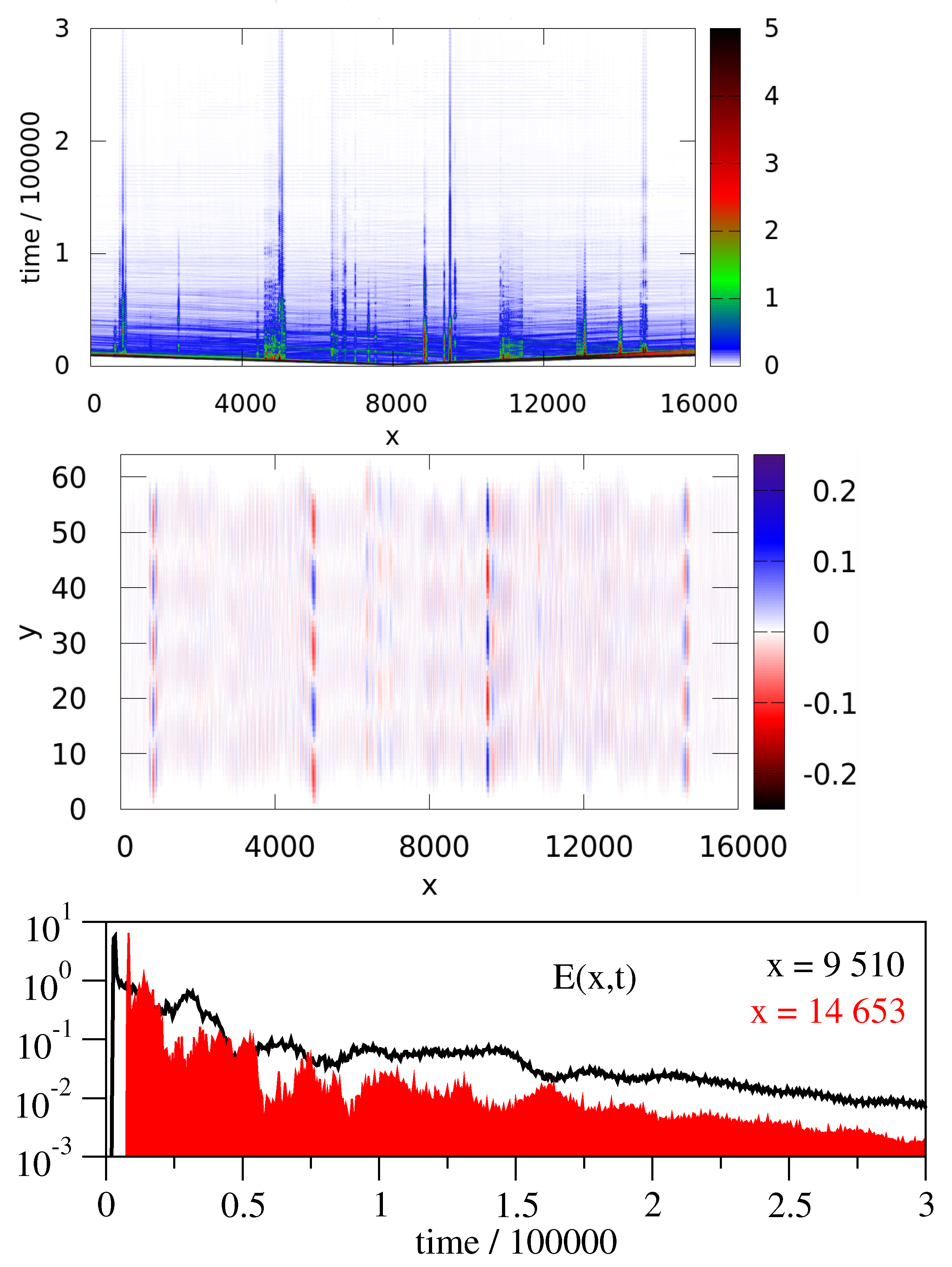
All of these measures show a clear signature of localization in numerical simulations [103]. As an example, Figure 5 shows the space and time evolution of normalized energy in the system excited by the heat pulse:
with parameters to assure that excited phonons are almost monochromatic. As is seen in the upper panel, part of the energy escapes the sample very quickly, being transmitted by ballistic phonons which do not scatter at the surface (Equation (14)). This energy is absorbed on the left and right boundaries and is not reflected back to the sample. Some parts of the energy, however, excited spatially localized resonances. The energy, trapped in the region of localization, might be re-emitted and absorbed by another resonance or reach the boundary of the sample. After a rather long period, only a few resonances survived, which are shown in the lower panel.
Figure 5 shows that a thin wire with corrugated surface contains quite a large number of localized phonons. As discussed in Ref. [103], the number of localized states increases when the frequency of the heat source increases, in agreement with frequency dependence of the transmission discussed in the previous section. The lifetime of localized resonances depends, of course, on the coupling of localized state to propagating waves [148], and of course, on the overlap of the localized waves of neighboring localized states.
Results shown in Figure 5 seem to suggest a straightforward inspiration for the observation of individual localized phonons in real experiments. However, owing to the high density of localized phonons, implementing this method might be difficult since it will require a very narrow frequency pulse.
5.3. Disorder Parameters and Universality
As mentioned above, there are many experimental parameters that can affect the thermal conductance of a thin wire with surface roughness. The experiments on silicon nanowires discussed above were characterized by several parameters, namely the rms height h of the roughness profile and a correlation length , as well as the diameter d of the wire, which is chosen to be much smaller than the length L of the wire. Assuming that the propagating phonons scatter from localized phonons as interpreted from the exact mapping, it was first conjectured in [104] that for a given width d of the sample the thermal conductivity is a universal function of a single parameter:
The universality was numerically verified, using the method discussed above, where the thermal conductance of different sets of the parameters but with the same value of were shown to be similar. To demonstrate the universality, Figure 6 presents the dependence of the integrated quantity:
where I serves as a “figure of merit” since the temperature dependence of the thermal conductivity is monotonic. Inset of Figure 6 indeed shows that the T-dependence of is universal. It was shown in Ref. [103] that the time evolution of energy after a pulse injected in the wire also satisfies this universality. This makes a theoretical study much easier, where one does not have to consider the effects of each of the parameters individually. It also makes experimental studies more flexible, where one can choose different sets of parameters to fabricate wires with the same effective strength of disorder. While the known parameters in existing experiments [119] seem to support this universality [104], there has been no systematic experimental study to confirm this important result to date.
5.4. Non-Linear Thermal Current
For a general frequency-dependent current , the thermal conductivity in the linear response regime (with ) is defined as
where is the Bose–Einstein distribution and is the Debye frequency. In the non-linear regime, for finite and possibly large , one can define an analogous quantity, namely:
The total current is a function of disorder as well as the lead temperatures.
Study of non-linear thermal transport in the presence of localized phonons requires using the full machinery of non-equilibrium quantum field theory [150]. In Ref. [151], non-equilibrium Green’s function techniques were used to evaluate the thermal current beyond the linear-response regime. For simplicity, only the effects of one localized phonon were considered, the width of the localized phonon chosen to be where it is assumed that the surface disorder can be characterized by the single parameter as defined in (25).
As expected, Figure 7 shows the thermal current with a clear dip in the assumed localized-phonon frequency, reducing the resulting thermal conductance. The normalized non-linear thermal conductivity as a function of the cold lead temperature (for a fixed ) shows more reduction for larger surface disorder (smaller ) at larger temperature difference. Unfortunately, there are no existing experiments for thermal current at large temperature differences. Systematic experimental studies of the thermal current with different values of as well as different strengths of surface disorder characterized by will be valuable in understanding the role of localized phonons in the context of thermoelectricity.
The model includes only one localized phonon at a fixed frequency and a fixed decay rate; a more realistic model should include a distribution of frequencies as well as the decay rates of the localized phonons characterized by the type of disorder. The model does not provide a dependence on the diameter of the wire, which is clearly observed in experiments [119,121,152]. It would be important to understand if/how the averaging over the impurities might lead to a diameter dependence of the thermal current, which will allow a deeper understanding of the relationship between surface disorder and localized phonons.
In addition, at high temperatures and large voltage differences, phonon–phonon interactions become important [153]. Beyond the couplings of the lead phonons with the phonons in the wire, it will also include three-phonon processes [125]. This is expected to be important especially if, e.g., the disorder leads to large scattering for high-energy phonons. Indeed, in a simulation of waves through disordered waveguides, Sanchez-Gil et al. [86] and Sadhu et al. [87] found evidence for ballistic, diffusive as well as localized waves to coexist within the same scale length, due to surface-type disorder. While low-energy acoustic phonons typically contribute more to thermal conductivity, high-energy phonons can become important at high temperatures [154]. The scattering of the high-energy optical phonons could therefore be important for thermoelectric devices.
6. Summary
Silicon nanowires with a particular type of surface roughness (electroless etching) have been experimentally shown to have very low thermal conductivity, which makes them a good candidate to be an efficient thermoelectric device. We review the theoretical claim and numerical evidence that this is due to the existence of localized phonons in the surface-disordered nanowires. An important consequence of these analytical and numerical studies is that although the surface roughness is characterized by several parameters, a single universal combination of these parameters describes the effective strength of the surface disorder. This is very useful for both theoretical and experimental studies of the effects of surface roughness on the thermal transport properties of the nanowire and needs to be experimentally investigated.
In addition to the lower thermal conductivity, we also review the idea that the overall efficiency of a thermoelectric device can be significantly improved by taking advantage of an interplay that exists only in the non-linear regime, between the material parameters (like the frequency dependent transmission function of the wire) and the thermodynamic parameters (like the temperatures and chemical potentials of the leads and the loads). The device is tunable in the sense that the efficiency can be maximized separately for each load, by tuning, e.g., by an applied gate voltage. Such a device is also scalable; increasing the number of wires kept in parallel and subject to the same gate voltage increases the power output. Experiments are needed to check whether it is indeed feasible to have both a high efficiency and a large power output in such a tunable nanowire-based thermoelectric device.
Author Contributions
Both authors contributed equally to original draft preparation, review and editing the text. Both authors have read and agreed to the published version of the manuscript.
Funding
Research performed in Slovakia was founded by Slovak Grand Agency Project n. 1/0101/20.
Acknowledgments
K.M. thanks their collaborators S. Abhinav, S. Hershfield and B. Nartowt.
Conflicts of Interest
The authors declare no conflict of interest.
References
- Harman, T.C.; Honig, J.M. Thermoelectric and Thermomagnetic Effects and Applications; McGraw-Hill: New York, NY, USA, 1967. [Google Scholar]
- Zebarjadi, M.; Esfarjani, K.; Dresselhaus, M.S.; Ren, Z.F.; Chen, G. Perspectives on thermoelectrics: From fundamentals to device applications. Energy Environ. Sci. 2012, 5, 5147. [Google Scholar] [CrossRef] [Green Version]
- Dubi, Y.; Di Ventra, M. Colloquium: Heat flow and thermoelectricity in atomic and molecular junctions. Rev. Mod. Phys. 2011, 83, 131. [Google Scholar] [CrossRef]
- Snyder, G.J.; Toberer, E.S. Complex thermoelectric materials. Nat. Mater. 2008, 7, 105. [Google Scholar] [CrossRef] [PubMed]
- Ashcroft, N.W.; Mermin, N.D. Solid State Physics; Holt, Rinehart and Winston: New York, NY, USA, 1976. [Google Scholar]
- Kim, T.-S.; Hershfield, S. Thermopower of an Aharonov-Bohm interferometer: Theoretical studies of quantum dots in the Kondo regime. Phys. Rev. Lett. 2002, 88, 136601. [Google Scholar] [CrossRef] [PubMed] [Green Version]
- Kim, T.-S.; Hershfield, S. Thermoelecteric effects of an Aharonov-Bohm interferometer with an embedded quantum dot in the Kondo regime. Phys. Rev. B 2003, 67, 165313. [Google Scholar] [CrossRef] [Green Version]
- Hicks, L.D.; Dresselhaus, M.S. Effect of quantum well structures on the thermoelectric figure of merit. Phys. Rev. B 1993, 47, 12727. [Google Scholar] [CrossRef]
- Hicks, L.D.; Harman, T.C.; Sun, X.; Dresselhaus, M.S. Experimental study of the effect of quantum well structure on the thermoelectric figure of merit. Phys. Rev. B 1996, 53, 10493(R). [Google Scholar] [CrossRef]
- Majumdar, A. Thermoelectricity in semiconductor nanostructures. Science 2004, 303, 777. [Google Scholar] [CrossRef]
- Paulsson, M.; Datta, S. Thermoelectric effect in molecular electronics. Phys. Rev. B 2003, 67, 241403(R). [Google Scholar] [CrossRef] [Green Version]
- Dresselhaus, M.; Chen, G.; Tang, M.Y.; Yang, R.; Lee, H.; Wang, D.; Ren, Z.; Fleurial, J.-P.; Gogna, P. New directions for low-dimensional thermoelectric materials. Adv. Mater. 2007, 19, 1043. [Google Scholar] [CrossRef]
- Reddy, P.; Jang, S.Y.; Segalman, R.A.; Majumdar, A. Thermoelectricity in molecular junctions. Science 2007, 315, 1568. [Google Scholar] [CrossRef]
- Abbout, A.; Ouerdane, H.; Goupil, C. Mesoscopic thermoelectric transport near zero transmission energies. Phys. Rev. B 2013, 87, 155410. [Google Scholar] [CrossRef] [Green Version]
- Glatz, A.; Beloborodov, I.S. Thermoelectric performance of weakly coupled granular materials. Europhys. Lett. 2009, 87, 57009. [Google Scholar] [CrossRef] [Green Version]
- Wu, K.; Rademaker, L.; Zaanen, J. Bilayer excitations in two-dimensional nanostructures for greatly enhanced thermoelectric efficiency. Phys. Rev. Appl. 2014, 2, 054013. [Google Scholar] [CrossRef] [Green Version]
- Sothman, B.; Sanchez, R.; Jordan, A.N. Thermoelectric energy harvesting with quantum dots. Nanotechnology 2015, 26, 032001. [Google Scholar] [CrossRef] [PubMed] [Green Version]
- Nakanishi, T.; Kato, T. Thermopower of a quantum dot in a coherent regime. J. Phys. Soc. Jpn. 2007, 76, 034715. [Google Scholar] [CrossRef] [Green Version]
- Wierzbicki, M.; Swirkowicz, R. Influence of interference effects on thermoelectric properties of double quantum dots. Phys. Rev. B 2011, 84, 075410. [Google Scholar] [CrossRef]
- Jordan, A.N.; Sothmann, B.; Sánchez, R.; Buttiker, M. Powerful and efficient energy harvester with resonant tunneling quantum dots. Phys. Rev. B 2013, 87, 075312. [Google Scholar] [CrossRef] [Green Version]
- Svensson, S.F.; Hoffmann, E.A.; Nakpathomkun, N.; Wu, P.M.; Xu, H.Q.; Nilsson, H.A.; Sanchez, D.; Kashcheyevs, V.; Linke, H. Nonlinear thermovoltage and thermocurrent in quantum dots. New J. Phys. 2013, 15, 105011. [Google Scholar] [CrossRef]
- Bergfield, J.P.; Solis, M.A.; Stafford, C.A. Giant thermoelectric effect from transmission supernodes. ACS Nano 2010, 4, 5314. [Google Scholar] [CrossRef] [Green Version]
- Koch, J.; von Oppen, F.; Oreg, Y.; Sela, E. Thermopower of single-molecule devices. Phys. Rev. B 2004, 70, 195107. [Google Scholar] [CrossRef] [Green Version]
- Karlström, O.; Linke, H.; Karlström, G.; Wacker, A. Increasing thermoelectric performance using coherent transport. Phys. Rev. B 2011, 84, 113415. [Google Scholar] [CrossRef] [Green Version]
- Murphy, P.; Mukerjee, S.; Moore, J. Optimal thermoelectric figure of merit of a molecular junction. Phys. Rev. B 2008, 78, 161406(R). [Google Scholar] [CrossRef] [Green Version]
- Entin-Wohlman, O.; Imry, Y.; Aharony, A. Three-terminal thermoelectric transport through a molecular junction. Phys. Rev. B 2010, 82, 115314. [Google Scholar] [CrossRef] [Green Version]
- Finch, C.M.; Garcia-Suarez, V.M.; Lambert, C.J. Giant thermopower and figure of merit in single-molecule devices. Phys. Rev. B 2009, 79, 033405. [Google Scholar] [CrossRef]
- Hicks, L.D.; Dresselhaus, M.S. Thermoelectric figure of merit of a one-dimensional quantum wire. Phys. Rev. B 1993, 47, 16631. [Google Scholar] [CrossRef]
- Kim, J.; Bahk, J.-H.; Hwang, J.; Kim, H.; Park, H.; Kim, W. Thermoelectricity in semiconductor nanowires. Phys. Status. Solidi RRL 2013, 7, 767. [Google Scholar] [CrossRef]
- Bossisio, R.; Fleury, G.; Pichard, J.-L. Gate-modulated thermopower in disordered nanowires. New J. Phys. 2014, 16, 035004. [Google Scholar] [CrossRef] [Green Version]
- Bossisio, R.; Gorini, C.; Fleury, G.; Pichard, J.-L. Using activated transport in parallel nanowires for energy harvesting and hot-spot cooling. Phys. Rev. Appl. 2015, 3, 054002. [Google Scholar] [CrossRef] [Green Version]
- Brovman, Y.M.; Small, J.; Hu, Y.; Fang, Y.; Lieber, C.M.; Kim, P. Electric field effect thermoelectric transport in individual silicon and Germanium/silicon nanowires. arXiv 2013, arXiv:1307.0249v1. [Google Scholar] [CrossRef] [Green Version]
- Mingo, N.; Yang, L.; Li, D.; Majumdar, A. Predicting the thermal conductivity of Si and Ge nanowires. Nano Lett. 2003, 3, 1713. [Google Scholar] [CrossRef]
- Meair, J.; Jacquod, P. Scattering theory of non-linear thermoelectricity in quantum coherent conductors. J. Phys. Condens. Matter 2013, 25, 082201. [Google Scholar] [CrossRef] [Green Version]
- Slack, G.A. CRC Handbook of Thermoelectrics; Rowe, D.M., Ed.; CRC Press: Boca Raton, FL, USA, 1995; p. 407. [Google Scholar]
- Takabatake, T.; Suekuni, K. Phonon-glass electron-crystal thermoelectric clathrates: Experiments and theory. arXiv 2014, arXiv:1402.5756. [Google Scholar] [CrossRef] [Green Version]
- Whitney, R.S. Non-linear thermoelectricity in point contacts at pinch off: A catastrophe aids cooling. Phys. Rev. B 2013, 88, 064302. [Google Scholar] [CrossRef] [Green Version]
- Zebarjadi, M.; Esfarjani, K.; Shakouri, A. Nonlinear Peltier effect in semiconductors. Appl. Phys. Lett. 2007, 91, 122104. [Google Scholar] [CrossRef] [Green Version]
- Sanchez, D.; Lopez, R. Nonlinear phenomena in quantum thermoelectrics and heat. Comptes Rendus Phys. 2016, 17, 1060. [Google Scholar] [CrossRef]
- Leijnse, M.; Wegewijs, M.R.; Flensberg, K. Nonlinear thermoelectric properties of molecular junctions with vibrational coupling. Phys. Rev. B 2010, 82, 045412. [Google Scholar] [CrossRef] [Green Version]
- Hershfield, S.; Muttalib, K.A.; Nartowt, B.J. Non-linear thermoelectric transport: A class of nano-devices for high efficiency and large power output. Phys. Rev. B 2013, 88, 085426. [Google Scholar] [CrossRef] [Green Version]
- Mahan, G.D.; Sofo, J.O. The best thermoelectric. Proc. Natl. Acad. Sci. USA 1996, 93, 7436. [Google Scholar] [CrossRef] [Green Version]
- Humphrey, T.E.; Linke, H. Reversible thermoelectric nanomaterials. Phys. Rev. Lett. 2005, 94, 096601. [Google Scholar] [CrossRef] [Green Version]
- Kim, R.; Datta, S.; Lundstrom, M.S. Influence of dimensionality on thermoelectric device. J. Appl. Phys. 2009, 105, 034506. [Google Scholar] [CrossRef]
- Jordan, A.N.; Sothmann, B.; Sanchez, R.; Büttiker, M. Rectification of thermal fluctuations in a chaotic cavity heat engine. Phys. Rev. B 2013, 87, 075312. [Google Scholar] [CrossRef] [Green Version]
- Whitney, R.S. The best quantum thermoelectric at finite power output. Phys. Rev. Lett. 2014, 112, 130601. [Google Scholar] [CrossRef] [PubMed] [Green Version]
- Nakpathomkun, N.; Xu, H.Q.; Linke, H. Thermoelectric efficiency at maximum power in low-dimensional systems. Phys. Rev. B 2010, 82, 235428. [Google Scholar] [CrossRef] [Green Version]
- Muralidharan, B.; Grifoni, M. Performance analysis of an interacting quantum dot thermoelectric setup. Phys. Rev. B 2012, 85, 155423. [Google Scholar] [CrossRef] [Green Version]
- Stadler, R.; Markussen, T. Controlling the transmission line shape of molecular t-stubs and potential thermoelectric applications. J. Chem. Phys. 2011, 135, 154109. [Google Scholar] [CrossRef] [Green Version]
- Muttalib, K.A.; Hershfield, S. Nonlinear thermoelectricity in disordered nanowires. Phys. Rev. Appl. 2015, 3, 054003. [Google Scholar] [CrossRef]
- Ludlam, J.J.; Taraskin, S.N.; Eliott, D.S.R. Disorder-induced vibrational localization. Phys. Rev. B 2003, 67, 132203. [Google Scholar] [CrossRef] [Green Version]
- Monthus, C.; Garel, T. Anderson localization in dimension d=1, 2, 3: Finite-size properties of the inverse participation rtatios of eigenstates. Phys. Rev. B 2010, 81, 224208. [Google Scholar] [CrossRef] [Green Version]
- Bertolotti, J.; Gottardo, S.; Wiersma, D.S.; Ghulinyan, M.; Pavesi, L. Optical necklace States in Anderson Localized 1D system. Phys. Rev. Lett. 2005, 94, 113903. [Google Scholar] [CrossRef]
- Hu, S.; Zhang, Z.; Jiang, P.; Chen, J.; Volz, S.; Nomura, M.; Li, B. Randomness-induced phonon localization in graphene heat conduction. Phys. Chem. Lett. 2018, 9, 3959. [Google Scholar] [CrossRef] [PubMed]
- Pailhes, S.; Euchner, H.; Giordano, V.M.; Debord, R.; Assy, A.; Gomes, S.; Bosak, A.; Machon, D.; Paschen, S.; de Boissieu, M. Localization of Propagative Phonons in a Perfectly Crystalline Solid. Phys. Rev. Lett. 2014, 113, 025506. [Google Scholar] [CrossRef] [Green Version]
- Song, P.H.; Kim, D.S. Localization of disordered phonon system: Anderson localization of optical phonons in AlxGa1−xAs. Phys. Rev. B 1996, 54, 2288(R). [Google Scholar] [CrossRef]
- Doring, F.; Eberl, C.; Schlenkrich, S.; Schlenkrich, F.; Hoffmann, S.; Liese, T.; Krebs, H.U.; Pisana, S.; Santos, T.; Schuhmann, H.; et al. Phonon localization in ultra thin layered structures. Appl. Phys. A 2015, 119, 11. [Google Scholar] [CrossRef]
- Mondal, W.R.; Berlijn, T.; Jarell, M.; Vidhyadhiraja, N.S. Phonon localization in binary alloys with diagonal and off-diagonal disorder: A cluster Green’s function approach. Phys. Rev. B 2019, 99, 134203. [Google Scholar] [CrossRef] [Green Version]
- Sun, Y.; Zhou, Y.; Han, J.; Liu, W.; Nan, C.; Lin, Y.; Hu, M.; Xu, B. Strong phonon localization in PbTe with dislocations and large deviation to Matthiessen’s rule. Comput. Mater. 2019, 5, 97. [Google Scholar] [CrossRef]
- Luckyanova, M.N.; Mendoza, J.; Lu, H.; Song, B.; Huang, S.; Zhou, J.; Li, M.; Dong, Y.; Zhou, H.; Garlow, J.; et al. Phonon localization in heat conduction. Sci. Adv. 2018, 4, eaat9460. [Google Scholar]
- Williams, M.L.; Marris, H.J. Numerical study of phonon localization in disordered systems. Phys. Rev. B 1985, 31, 4508. [Google Scholar] [CrossRef] [PubMed]
- Anderson, P.W. Absence of Diffusion in Certain Random Lattices. Phys. Rev. 1958, 109, 1492. [Google Scholar] [CrossRef]
- van Rossum, M.C.W.; Nieuwenhuizen, T.M. Multiple scattering of classical waves: Microscopy mesoscopy and diffusion. Rev. Mod. Phys. 1999, 71, 313. [Google Scholar] [CrossRef] [Green Version]
- Lee, P.A.; Ramakrishnan, T.V. Disordered electronic systems. Rev. Mod. Phys. 1985, 57, 287. [Google Scholar] [CrossRef]
- Kramer, B.; MacKinnon, A. Localization: Theory and experiment. Rep. Progr. Phys. 1993, 56, 1469. [Google Scholar] [CrossRef]
- Abrahams, E. (Ed.) 50 Years of Anderson Localization; World Scientific: Singapore, 2010. [Google Scholar]
- Soukoulis, C.M.; Economou, E.N.; Grest, G.S.; Cohen, M.H. Existence of Anderson Localization of Classical Waves in a Random Two-Component Medium. Phys. Rev. Lett. 1989, 62, 575. [Google Scholar] [CrossRef] [PubMed]
- John, S. Electromagnetic Absorption in a Disordered Mediu near a Photon Mobility Edge. Phys. Rev. Lett. 1984, 53, 2169. [Google Scholar] [CrossRef]
- John, S. Localization of light. Phys. Today 1991, 44, 32–40. [Google Scholar] [CrossRef]
- Sheng, P.; Zhoy, M.; Zhang, Z.-Q. Phonon transport in strongly-scattering media. Phys. Rev. Lett. 1994, 72, 234. [Google Scholar] [CrossRef] [Green Version]
- Akkermans, E.; Montambaux, G. Mesoscopic Physics of Electrons and Photons; Cambridge University Press: Cambridge, UK, 2007. [Google Scholar]
- Sheng, P. Introduction to Wave Scattering, Localization and Mesoscopis Phenomena; Springer: Berlin/Heidelberg, Germany; New York, NY, USA, 2006. [Google Scholar]
- Lagendijk, A.; vanTiggelen, B.; Wiersma, D.S. Fifty years of Anderson localization. Phys. Today 2009, 62, 24–29. [Google Scholar] [CrossRef] [Green Version]
- Lopez, M.; Clement, J.-F.; Szriftgiser, P.; Garreau, J.C.; Delande, D. Expermental test of universality of the Anderson Transition. Phys. Rev. Lett. 2012, 101, 095701. [Google Scholar] [CrossRef] [Green Version]
- Savic, I.; Mingo, N.; Stewart, D.A. Phonon Transport in isotope-disordered carbon and boron-nitride nanotubes: Is localization observable? Phys. Rev. Lett. 2008, 101, 165502. [Google Scholar] [CrossRef] [Green Version]
- Chang, C.W.; Okawa, D.; Garcia, H.; Majumdar, A.; Zettl, A. Breakdown Fourier’s Law Nanotub. Therm. Conductors. Phys. Rev. Lett. 2008, 101, 075903. [Google Scholar] [CrossRef] [Green Version]
- Larose, E.; Margerin, L.; van Tiggelen, B.A.; Campillo, M. Weak Localization of Seismic Waves. Phys. Rev. Lett. 2004, 93, 048501. [Google Scholar] [CrossRef]
- Hu, H.; Strybulevych, A.; Page, J.H.; Skipetrov, S.E.; van Tiggelen, B.A. Localization of ultrasound in a three-dimensional elastic network. Nat. Phys. 2008, 4, 945. [Google Scholar] [CrossRef]
- Upadhyaya, N.; Amir, A. Disorder engineering: From structural coloration to acoustic filters. Phys. Rev. Mater. 2018, 2, 075201. [Google Scholar] [CrossRef]
- Markussen, T.; Jauho, A.-P.; Brangbyge, M. Surface-Decorated Silicon Nanowires: A Route to High-ZT Thermoelectrics. Phys. Rev. Lett. 2009, 103, 055502. [Google Scholar] [CrossRef] [PubMed] [Green Version]
- Chaney, D.; Castellano, A.; Bosak, A.; Bouchet, J.; Bottin, F.; Dorado, B.; Paolasini, L.; Rennie, S.; Bell, C.; Springell, R.; et al. Tuneable correlated disorder in alloys. Phys. Rev. Mater. 2021, 5, 035004. [Google Scholar] [CrossRef]
- Xiong, S.; Saaskilahti, K.; Kosevich, Y.A.; Han, H.; Donadio, D.; Volz, S. Blocking phonon transport by structural resonances in alloy-based nanophononic metamaterials lead to ultralow thermal conductivity. Phys. Rev. Lett. 2016, 117, 025503. [Google Scholar] [CrossRef] [PubMed]
- Garcia-Martin, A.; Lopez-Ciudad, T.; Saenz, J.J.; Nieto-Vesperinas, M. Statistical Distribution of Intensities reflected from disordered media. Phys. Rev. Lett. 1998, 81, 329. [Google Scholar] [CrossRef] [Green Version]
- Garcia-Martin, A.; Torres, J.A.; Saenz, J.J.; Nieto-Vesperinas, M. Intensity distribution of modes in surface corrugated waveguides. Phys. Rev. Lett. 1998, 80, 4165. [Google Scholar] [CrossRef] [Green Version]
- Lio, G.E.; Ferraro, A.; Ritacco, T.; Aceti, D.M.; De Luca, A.; Giocondo, M.; Caputo, R. Leveraging on ENZ Metamaterials to Achieve 2D and 3D Hyper-Resolution in Two-Photon Direct Laser Writing. Adv. Mater. 2021, 33, 2008644. [Google Scholar] [CrossRef]
- Sanchez-Gil, J.A.; Freilikher, V.; Yurkevich, I.; Maradudin, A.A. Coexistence of ballistic transport, diffusion and localization in surface disordered waveguides. Phys. Rev. Lett. 1998, 80, 948. [Google Scholar] [CrossRef]
- Sadhu, J.; Sinha, S. Room-temperature phonon boundary scattering below the Casimir limit. Phys. Rev. B 2011, 84, 115450. [Google Scholar] [CrossRef] [Green Version]
- Feilhauer, J.; Moško, M. Quantum and Boltzmann transport in a quasi-one-dimensional wire with rough edges. Phys. Rev. B 2011, 83, 245328. [Google Scholar] [CrossRef] [Green Version]
- Izrailev, F.M.; Krokhin, A.A.; Makarov, N.M. Anomalous localization in low-dimensional systems with correlated disorder. Phys. Rep. 2012, 512, 125. [Google Scholar] [CrossRef] [Green Version]
- Dietz, O.; Stockmann, H.-J.; Kuhl, U.; Izrailev, F.M.; Makarov, N.M.; Doppler, J.; Libisch, F.; Rotter, S. Surface scattering and band gaps in rough nanowires and waveguides. Phys. Rev. B 2012, 86, R201106. [Google Scholar] [CrossRef] [Green Version]
- Santamore, D.H.; Cross, M.C. Effect of Phonon Scattering by Surface Roughness on the Universal Thermal Conductance. Phys. Rev. Lett. 2001, 87, 115502. [Google Scholar] [CrossRef] [Green Version]
- Santamore, D.H.; Cross, M.C. Effect of surface roughness on the universal thermal conductance. Phys. Rev. B 2001, 63, 184306. [Google Scholar] [CrossRef] [Green Version]
- Pendry, J.B. Quasi-extended electron states in strongly disordered systems. J. Phys. C Solid State Phys. 1987, 20, 733. [Google Scholar] [CrossRef]
- Skipetrov, S.E.; Sokolov, I.M. Ioffe-Regel criterion of Anderson localization in the model of resonant point scatterers. Phys. Rev. B 2018, 98, 064207. [Google Scholar] [CrossRef] [Green Version]
- Fan, S.; Joannopoulos, J.D. Analysis of guided resonances in photonic crystal slabs. Phys. Rev. B 2002, 65, 235112. [Google Scholar] [CrossRef] [Green Version]
- Poddubny, A.N.; Rybin, M.V.; Limonov, M.F.; Kivshar, Y. Fano interference governs wave transport in disordered systems. Nat. Commun. 2012, 3, 914. [Google Scholar] [CrossRef] [PubMed]
- Markoš, P. Fano resonances and band structure of two dimensional photonic structures. Phys. Rev. A 2015, 92, 043814. [Google Scholar] [CrossRef] [Green Version]
- Maier, S.A. Plasmonics: Fundamentals and Applications; Springer Science: Berlin, Germany, 2007. [Google Scholar]
- Lio, G.E.; De Luca, A.; Umeton, C.P.; Caputo, R. Opto-mechanically induced thermoplasmonic response of unclonable flexible tags with hotspot fingerprint. J. Appl. Phys. 2020, 128, 093107. [Google Scholar]
- Baffou, G. Thermoplasmonics; World Scientific: Singapore, 2017. [Google Scholar]
- Bliokh, K.Y.; Bliokh, Y.P.; Freilikher, V. Resonances in 1D disordered systems: Localization of energy and resonant transmission. J. Am. Opt. Soc. B 2004, 21, 113. [Google Scholar] [CrossRef] [Green Version]
- Bliokh, K.Y.; Bliokh, Y.P.; Freilikher, V.; Savelev, S.; Nori, F. Unusual Resonators: Plasmonics, Metamaterials, and Random Media. Rev. Mod. Phys. 2008, 80, 1201. [Google Scholar] [CrossRef] [Green Version]
- Markoš, P.; Muttalib, K.A. Phonon localization in surface-roughness dominated nanowires. Phys. Rev. B 2019, 99, 134208. [Google Scholar] [CrossRef] [Green Version]
- Markoš, P.; Muttalib, K.A. Universality of phonon transport in nanowires dominated by surface-roughness. Phys. Rev. B 2018, 97, 085423. [Google Scholar] [CrossRef] [Green Version]
- Ozisik, M.N.; Tzou, D.Y. On the Wave Theory in Heat Conduction. Trans. ASME 1994, 116, 526. [Google Scholar] [CrossRef]
- Lepri, S.; Livi, R.; Politi, A. Thermal conduction in classical low-dimensional lattices. Phys. Rep. 2003, 377, 1. [Google Scholar] [CrossRef] [Green Version]
- Zebarjadi, M.; Yang, J.; Lukas, K.; Kozinsky, B.; Yu, B.; Dresselhaus, M.S.; Opeli, C.; Ren, Z.; Chen, G. Role of phonon dispersion in studying phonon mean free paths in skutterudities. J. Appl. Phys. 2012, 112, 044305. [Google Scholar] [CrossRef]
- Zhang, H.; Hua, C.; Ding, D.; Minnich, A.J. Length Dependent Thermal Conductivity Measurements Yiels Phonon Mean Free Path Spectra in Nanostructures. Sci. Rep. 2015, 5, 9121. [Google Scholar] [CrossRef] [PubMed] [Green Version]
- Minnich, A.J. Determining Phonon Mean Free Path from Observations of Quasiballistic Thermal Transport. Phys. Rev. Lett. 2012, 109, 205901. [Google Scholar] [CrossRef]
- Minnich, A.J.; Dresselhaus, M.S.; Ren, Z.F.; Chen, G. Bulk nanostructured thermoelectric materials: Current research and future prospects. Energy Environ. Sci. 2009, 2, 466. [Google Scholar] [CrossRef]
- Regner, K.T.; Sellan, D.P.; Su, Z.; Amon, C.H.; McGaughey, A.J.H.; Malen, J.A. Broadband phonon mean free path contributions to thermal conductivity measured using frequency domain thermoreflectance. Nat. Commun. 2013, 4, 1640. [Google Scholar] [CrossRef] [Green Version]
- Malthora, A.; Maldovan, M. Impact of Phonon Surface Scattering on Thermal Energy Distribution of Si and SiGe Nanowires. Sci. Rep. 2016, 6, 25818. [Google Scholar] [CrossRef]
- Zhao, Y.; Liu, D.; Chen, J.; Zhu, L.; Belianinov, A.; Ovchinnikova, O.S.; Unocic, R.R.; Burch, M.J.; Kim, S.; Hao, H.; et al. Engineering the thermal conductivity along an individual silicon nanowire by selective helium ion irradation. Nat. Commun. 2017, 8, 15919. [Google Scholar]
- Markussen, T.; Jauho, A.-P.; Brandbyge, M. Heat conductance is strongly anisotropic for pristine silicon nanowires. Nano Lett. 2008, 8, 3771. [Google Scholar] [CrossRef] [PubMed] [Green Version]
- Jiang, P.; Ouyang, Y.; Ren, W.; Yu, C.; He, J.; Chen, J. Total-transmission and total-reflection of individual phonons in phononic crystal nanostructures. APLMater 2021, 9, 040703. [Google Scholar]
- Ferraro, A.; Cerza, P.; Mussi, V.; Maiolo, L.; Convertino, A.; Caputo, R. Efficient Photothermal Generation by Nanoscale Light Trapping in a Forest of Silicon Nanowires. J. Phys. Chem. C 2021, 125, 14134. [Google Scholar] [CrossRef]
- Boukai, A.I.; Bunimovich, Y.; Tahir-Kheli, J.; Yu, J.-K.; Goddard, W.A., III; Heath, J.R. Silicon nanowires as efficient thermoelectric materials. Nature 2008, 451, 168. [Google Scholar] [CrossRef]
- Li, D.; Wu, Y.; Kim, P.; Shi, L.; Yang, P.; Majumdar, A. Thermal conductivity of individual silicon nanowires. App. Phys. Lett. 2003, 83, 2934. [Google Scholar] [CrossRef]
- Hochbaum, A.I.; Chen, R.; Delgado, R.D.; Liang, W.; Garnett, E.C.; Najarian, M.; Majumdar, A.; Yang, P. Enhanced thermoelectric performance of rough silicon nanowires. Nature 2008, 451, 163. [Google Scholar] [CrossRef] [PubMed]
- Chen, R.; Hochbaum, A.I.; Murphy, P.; Moore, J.; Yang, P.; Majumdar, A. Thermal Conductance of Thin Silicon Nanowires. Phys. Rev. Lett. 2008, 101, 105501. [Google Scholar] [CrossRef] [PubMed] [Green Version]
- Lim, J.; Hippalgaonkar, K.; Andrews, S.C.; Majumdar, A. Quantifying surface roughness effects on phonon transport in silicon nanowires. Nano Lett. 2012, 12, 2475. [Google Scholar] [CrossRef] [PubMed]
- Heron, J.-S.; Fournier, T.; Mingo, N.; Bourgeois, O. Mesoscopic size effects on the thermal conductance of silicon nanowires. Nano Lett. 2009, 9, 1861. [Google Scholar] [CrossRef] [PubMed]
- Blanc, C.; Rajabpour, A.; Volz, S.; Fournier, T.; Bourgeois, O. Phonon heat conduction in corrugated silicon nanowires below the Casimir limit. Appl. Phys. Lett. 2013, 103, 043109. [Google Scholar] [CrossRef] [Green Version]
- Blanc, C.; Heron, J.-S.; Fournier, T.; Bourgeois, O. Heat transmission between a profiled nanowire and a thermal bath. App. Phys. Lett. 2014, 105, 043106. [Google Scholar] [CrossRef]
- Mingo, N. Anharmonic phonon flow through molecular-sized junctions. Phys. Rev. B 2006, 74, 125402. [Google Scholar] [CrossRef]
- Moore, A.L.; Saha, S.K.; Prasher, R.S.; Shi, L. Phonon backscattering and thermal conductivity suppression in sawtooth nanowires. Appl. Phys. Lett. 2008, 93, 083112. [Google Scholar] [CrossRef] [Green Version]
- Martin, P.; Aksamija, Z.; Popp, E.; Ravioli, U. Impact of phonon-surface roughness scattering on thermal conductivity of thin nanowires. Phys. Rev. Lett. 2009, 102, 125503. [Google Scholar] [CrossRef]
- Carrete, J.; Gallego, L.J.; Varela, L.M.; Mingo, N. Surface roughness and thermal conductivity of semiconductor nanowires: Going below Casimir limit. Phys. Rev. B 2011, 84, 075403. [Google Scholar] [CrossRef] [Green Version]
- Markussen, T.; Jauho, A.-P.; Brandbyge, M. Electron and phonon transport in silicon nanowires: Atomic approach to thermoelectric properties. Phys. Rev. B 2009, 79, 035415. [Google Scholar] [CrossRef] [Green Version]
- Markussen, T.; Rurali, R.; Brandbyge, M.; Jauho, A.-P. Electronic transport through Si nanowires: Role of bulk and surface disorder. Phys. Rev. B 2006, 74, 245313. [Google Scholar] [CrossRef] [Green Version]
- Bauer, D.; Luisier, M. Influence of disorder and surface roughness on the electrical and thermal properties of lithiated silicon nanowires. J. Appl. Phys. 2020, 127, 135101. [Google Scholar] [CrossRef]
- Svizhenko, A.; Leu, P.; Cho, K. Effect of growth orientation and surface roughness on electron transport in silicon nanowires. Phys. Rev. B 2007, 75, 125417. [Google Scholar] [CrossRef]
- Maurer, L.N.; Mei, S.; Knezevic, I. Rayleigh waves, surface disorder, and phonon localization in nanostructures. Phys. Rev. B 2016, 94, 045312. [Google Scholar] [CrossRef] [Green Version]
- Akguc, G.B.; Gong, J. Wave-scattering formalism for thermal conductance in thin wires with surface disorder. Phys. Rev. B 2009, 80, 195408. [Google Scholar] [CrossRef]
- Lacroix, D.; Joulain, K.; Damian, T.; Lemonnier, D. Monte Carlo simulation of phonon confinement in silicon nanostructures: Application to the determination of the thermal conductivity of silicon nanowires. Appl. Phys. Lett. 2006, 89, 103104. [Google Scholar] [CrossRef]
- Donadio, D.; Galli, G. Atomistic Simulations of Heat Transport in Silicon Nanowires. Phys. Rev. Lett. 2009, 102, 195901. [Google Scholar] [CrossRef]
- He, Y.; Galli, G. Microscopic Origin of the Reduced Thermal Conductivity of Silicon Nanowires. Phys. Rev. Lett. 2012, 108, 215901. [Google Scholar] [CrossRef] [Green Version]
- Zushi, T.; Ohmori, K.; Yamada, K.; Watanabe, T. Effect of a SiO2 layer on the thermal transport properties of <100> Si nanowires: A molecular dynamics study. Phys. Rev. B 2015, 91, 115308. [Google Scholar]
- Liu, L.; Chen, X. Effect of surface roughness on thermal conductivity of silicon nanowires. J. Appl. Phys. 2010, 107, 033501. [Google Scholar] [CrossRef]
- Hyun, O.J.; Shin, M.; Jang, M.-G. Phonon transport in Si nanowires with elastically dissimilar barriers. J. Appl. Phys. 2012, 111, 044304. [Google Scholar] [CrossRef]
- Murphy, P.G.; Moore, J.E. Coherent phonon scattering effects on thermal transport in thin semiconductor nanowires. Phys. Rev. B 2007, 76, 155313. [Google Scholar] [CrossRef] [Green Version]
- Ando, T. Quantum point contact in magnetic fields. Phys. Rev. B 1991, 44, 8017. [Google Scholar] [CrossRef] [PubMed]
- Pendry, J.B.; MacKinnon, A.; Roberts, P.J. Universality classes and fluctuation in disordered systems. Proc. R. Soc. Lond. Ser. A 1992, 437, 67. [Google Scholar]
- Markoš, P. Numerical analysis of Anderson localization. Acta Phys. Slovaca 2006, 56, 561. [Google Scholar] [CrossRef] [Green Version]
- Muttalib, K.A.; Abhinav, S. Suppressing phonon transport in nanowires: A simple model for phonon-surface-roughness interaction. Phys. Rev. B 2017, 96, 075403. [Google Scholar] [CrossRef] [Green Version]
- Tesanovich, Z.; Jaric, M.V.; Maekawa, S. Quantum transport and surface scattering. Phys. Rev. Lett. 1986, 57, 2760. [Google Scholar] [CrossRef]
- Abrikosov, A.A.; Gorkov, L.P.; Dzyaloshinskii, I.E. Methods of Quantum Field Theory in Statistical Physics; Courier Corporation: Chelmsford, MA, USA, 1975. [Google Scholar]
- Kottos, T. Statistics of resonances and delay time in random media: Beyond random matrix theory. J. Phys. A Math. Gen. 2005, 38, 10761. [Google Scholar] [CrossRef]
- Clayton, R.; Enquist, B. Absorbing boundary conditions for acoustic and elastic wave equations. Bull. Seism. Soc. Am. 1977, 67, 1529. [Google Scholar]
- Rammer, J.; Smith, H. Quantum field-theoretical methods in transport theory of metals. Rev. Mod. Phys. 1986, 58, 323. [Google Scholar] [CrossRef]
- Abhinav, S.; Muttalib, K.A. Non-equilibrium phonon transport in surface-roughness dominated nanowires. J. Phys. Commun. 2019, 3, 105010. [Google Scholar] [CrossRef] [Green Version]
- Vakulov, D.; Gireesan, S.; Swinkels, M.Y.; Chavez, R.; Vogelaar, T.; Torres, P.; Campo, A.; De Luca, M.; Verheijen, M.A.; Koelling, S.; et al. Ballistic phonons in ultrathin nanowires. Nano Lett. 2020, 20, 2703. [Google Scholar] [CrossRef]
- Galperin, M.; Nitzan, A.; Ratner, M. Heat conduction in molecular transport junctions. Phys. Rev. B 2007, 75, 155312. [Google Scholar] [CrossRef] [Green Version]
- Tian, Z.; Esfarjani, K.; Shiomi, J.; Henry, A.S.; Chen, G. On the importance of optical phonons to thermal conductivity in nanostructures. Appl. Phys. Lett. 2011, 99, 053122. [Google Scholar] [CrossRef]
- Hyldgaard, P.; Hershfield, S.; Davies, J.H.; Wilkins, J.W. Resonant tunneling with an electron-phonon interaction. Ann. Phys. 1994, 236, 1. [Google Scholar] [CrossRef]
- Prange, R.E.; Kadanoff, L.P. Transport theory for electron-phonon interactions in metals. Phys. Rev. 1964, 134, A566. [Google Scholar] [CrossRef] [Green Version]
- Mitra, A.; Aleiner, I.; Millis, A.J. Phonon effects in molecular transistors: Quantal and classical treatment. Phys. Rev. B 2004, 69, 245302. [Google Scholar] [CrossRef] [Green Version]
Figure 1.
Cartoon of a thermoelectric device.

Figure 3.
Left panel: transmission function for a weakly disordered wire of length in units of the lattice spacing and localization length L. The lower impurity band edge is at Difference of the Fermi functions (solid black curve) with , , , and . A gate voltage corresponding to will move and align it with . Right panel: the efficiency and power output P as a function of the gate voltage, using the parameters chosen in the left panel. Maximum power occurs at , where the lower band edge aligns with . At the same time, there exists a wide range of for which and P is near the peak value [50].

Figure 5.
Space and time evolution of normalized energy in a weakly surface disordered sample, with = (64, 200, 6, 16,000). A set of resonances excited by an external source with period corresponds to localized phonons with eigenfrequencies lying in the lower part of the acoustic frequency band. Note the length of the sample L = 16,000 and the time of simulations, in comparison with the period of excited acoustic waves. Perfectly absorbed boundary conditions [149] were implemented at the left and right boundaries of the wire in order to eliminate any reflection of the energy: Upper panel: the space–time dependence of the amplitude of the acoustic wave; Middle panel: the spatial distribution of energy at a time t = 194,400; Lower panel: time evolution of the energy at x = 9510 and x = 14,653. Localized states are first excited by phonons from the source (the narrow maxima at the beginning of the time evolution) which then exchanges their energy with other localized states in its neighborhood. The energy of a localized state close to the boundary exponentially decreases due to loss through the right boundary of the sample [103].

Figure 6.
Integral I, given by Equation (26) of the thermal conductance over frequency for wires with different combinations of the disorder parameters. Overlapping region confirms the universality (25). The size of the wire is . Data for the same symbol correspond to samples with different surface corrugation h. Inset confirms that two samples with the same value of possess the same thermal conductance for any temperature (shown by solid lines and dots, respectively) [104].

Figure 7.
Effect of a single localized phonon on the thermal current as a function of frequency for various surface disorder (top panel) and the non-linear thermal conductivity as a function of the temperature of the cold lead for various temperature differences (bottom panel). Frequency and temperature are given in units introduced in the text. Reprinted from Ref. [151].

Publisher’s Note: MDPI stays neutral with regard to jurisdictional claims in published maps and institutional affiliations. |
© 2021 by the authors. Licensee MDPI, Basel, Switzerland. This article is an open access article distributed under the terms and conditions of the Creative Commons Attribution (CC BY) license (https://creativecommons.org/licenses/by/4.0/).
Share and Cite
MDPI and ACS Style
Markoš, P.; Muttalib, K. Non-Linear Thermoelectric Devices with Surface-Disordered Nanowires. Appl. Nano 2021, 2, 162-183. https://0-doi-org.brum.beds.ac.uk/10.3390/applnano2030013
AMA Style
Markoš P, Muttalib K. Non-Linear Thermoelectric Devices with Surface-Disordered Nanowires. Applied Nano. 2021; 2(3):162-183. https://0-doi-org.brum.beds.ac.uk/10.3390/applnano2030013
Chicago/Turabian StyleMarkoš, Peter, and Khandker Muttalib. 2021. "Non-Linear Thermoelectric Devices with Surface-Disordered Nanowires" Applied Nano 2, no. 3: 162-183. https://0-doi-org.brum.beds.ac.uk/10.3390/applnano2030013