Carbon Allotropes as ITO Electrode Replacement Materials in Liquid Crystal Devices


Department of Physics and Astronomy, University of Manchester, Oxford Road, Manchester M139PL, UK
C 2020, 6(4), 80; https://0-doi-org.brum.beds.ac.uk/10.3390/c6040080
Submission received: 21 November 2020
/
Accepted: 8 December 2020
/
Published: 10 December 2020
(This article belongs to the Special Issue Carbon Based Electrochemical Devices)
Abstract
:Indium tin oxide (ITO)-free optoelectronic devices have been discussed for a number of years in the light of a possible indium shortage as demand rises. In particular, this is due to the largely increased number of flat panel displays and especially liquid crystal displays (LCDs) being produced for home entertainment TV and mobile technologies. While a shortage of primary indium seems far on the horizon, nevertheless, recycling has become an important issue, as has the development of ITO-free electrode materials, especially for flexible liquid crystal devices. The main contenders for new electrode technologies are discussed with an emphasis placed on carbon-based materials for LCDs, including composite approaches. At present, these already fulfil the technical specifications demanded from ITO with respect to transmittance and sheet resistance, albeit not in relation to cost and large-scale production. Advantages and disadvantages of ITO-free technologies are discussed, with application examples given. An outlook into the future suggests no immediate transition to carbon-based electrodes in the area of LCDs, while this may change in the future once flexible displays and environmentally friendly smart window solutions or energy harvesting building coverings become available.
Keywords:
ITO; electrode; nanotubes; graphene; liquid crystals; metal nanowires; conducting polymers
1. Introduction
Indium was discovered in 1863 by Reich and Richter, who were two chemists studying the ores from the mines of the region around Freiberg in Germany. It is one of the critical metals for the modern, technologically oriented industry [1]. Mined from zinc sulphide ores, it is a minor component and produced during the refinement process of the major component, zinc. In technology, it finds its main uses in the production of transparent electrodes as an indium–tin alloy, ITO, or indium tin oxide, consisting of indium oxide (In2O3) and tin oxide (SnO2) at a mass ratio of 9:1, or 74% In, 8% Sn, and 18% O2 [2].
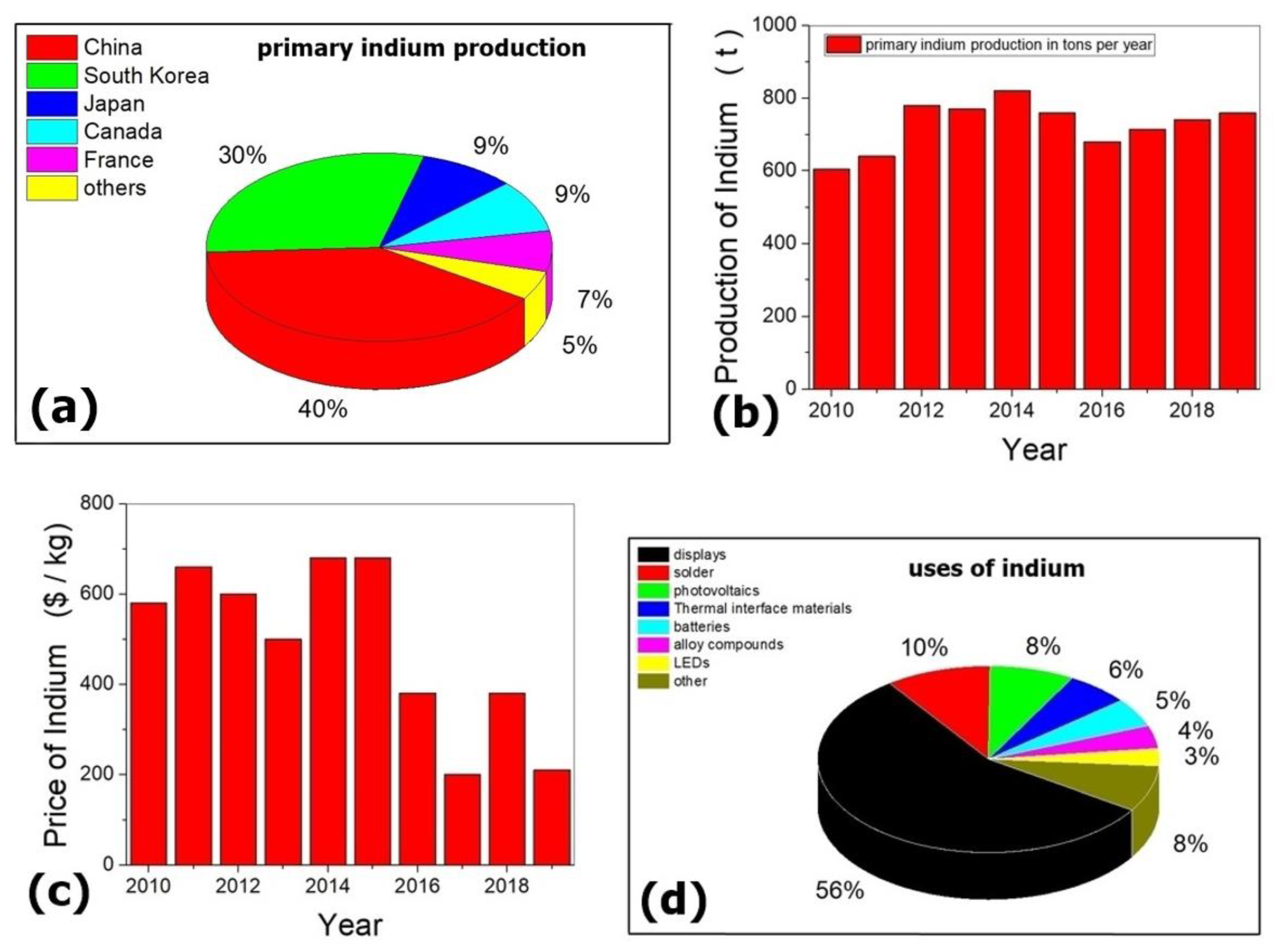
The primary indium production is mainly located in China, South Korea, Japan, and Canada (Figure 1a), which contribute nearly all of the world’s current annual indium production of roughly 800 tons per year [3]. This amount has been relatively stable and constant over the last decade (Figure 1b) [4], while during the three decades before (1980–2010), the production has increased more than tenfold. The constant primary indium production should not disguise an increasing demand of the metal, even over the last decade. This has several reasons; firstly, there has been an increase in secondary indium production through recycling, and secondly, stored overproduction in China has been released onto the world market. It is thought that the secondary indium production has by now reached a similar level as the primary production, fulfiling the current total world demand of indium, which is in the order of about 1300 tons per year. While prices had been steeply increasing during the beginning of the 21st century, they have been dropping recently from about $600 per kg to roughly half of that value (Figure 1c) [4] due to reasons mentioned above. The main end-use of indium by far is found in the display technology, having shifted nearly exclusively from CRTs (cathode ray tubes) to flat panel displays (FPDs) over the last two decades. This is followed by the use as solder and in photovoltaics and solar cells (Figure 1d) [5]. Since the display market is by a large margin the main consumer of indium in the form of ITO, this paper will place an emphasis on this technology.
In recent years, there has been a controversial discussion about the exhaustion of indium supplies for the technology industry. While first claims of the supply of indium being at threat already in the mid 2020s have proven to be incorrect [6], it is estimated that imminent shortages may occur over the next one or two generations, approximately around the year 2050 [7]. Of course, such an estimate is quite hard to make, as it does not only rely on an estimation of the remaining primary indium deposits and the rate of increased consumption—one also has to take into account increasing incentives for recycling through policy changes, the price development of indium, and therefore the viability of different recycling processes and technological developments. This is just naming some of the factors, which have a relatively large margin of error for prediction. For example, during the sputtering process of ITO, roughly 90% of the material actually remains in the production machine, which is viable for industry to be recycled. However, the recycling of indium from end-of-life displays is not yet viable. This may change as the resources become increasingly scarce and the price of indium increases. Yet, the recycling of display components in general may also be brought about through political measures and the drive for greener technologies.
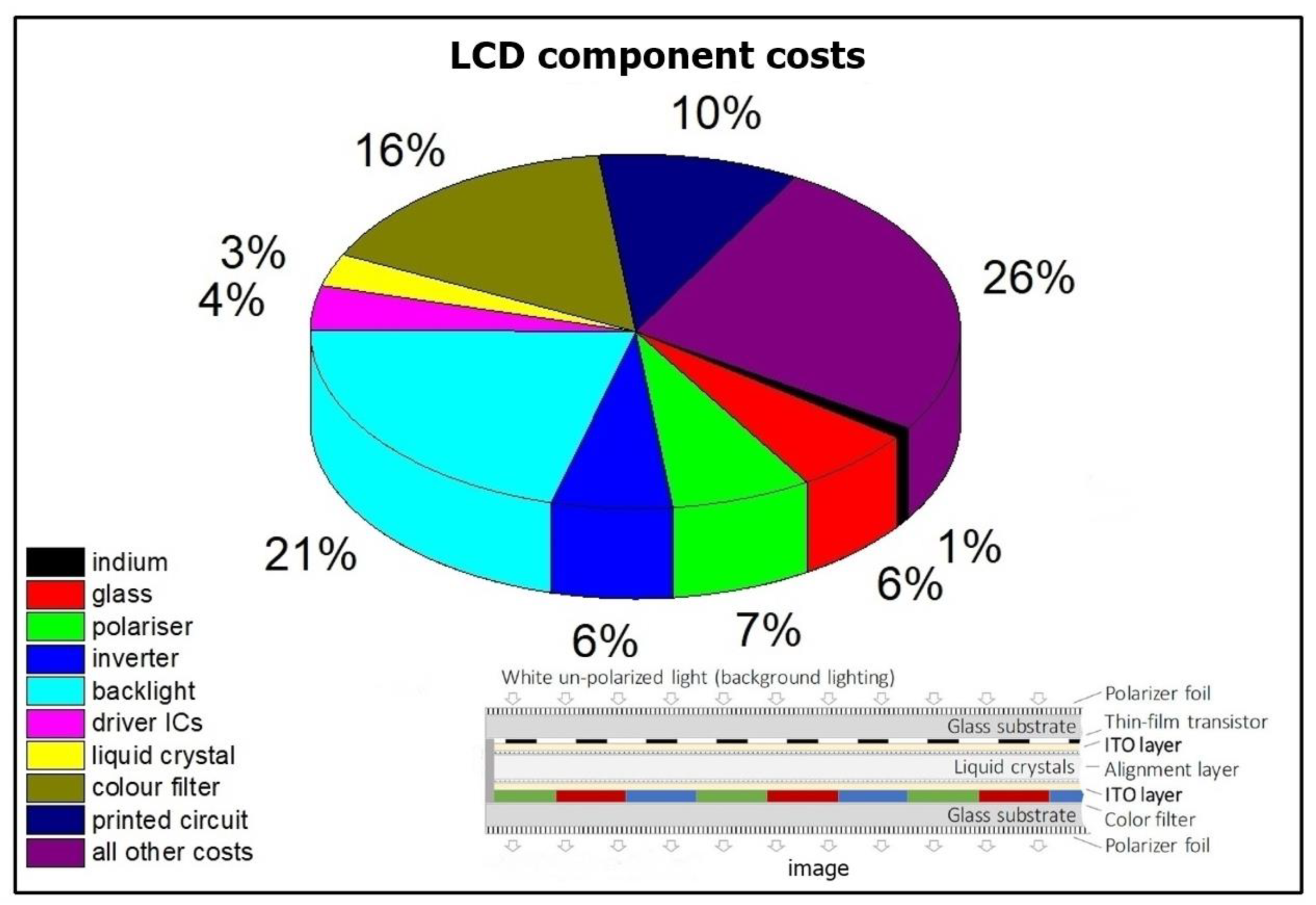
This can illustratively be seen by the real cost of the different components installed in a liquid crystal flat panel display. The actual display sandwich cell is constructed of two ITO-coated glass substrates onto which polarizer films are laminated. The ITO films act as transparent, conductive electrodes. The substrates are glued together, being kept at a distance of approximately 5 μm through spacers. Alignment layers, often rubbed polyimide, assure a uniform orientation of the liquid crystal, which is filled in the narrow sandwich cell gap. One of the glass substrates hosts an arrays of thin film transistors (TFT) to address individual pixels and produce grey-scale levels, while the other contains red–green–blue (RGB) colour filters providing the overall video rate colour images of, for example, a movie (see inset of Figure 2). In contrast to popular belief, it is neither the liquid crystal nor the indium of the ITO-coated glass sheets that carry the main cost of a display. The most expensive components of a flat panel display are in fact the backlight, and the colour filter, if one ignores the indirect, personnel, and sales costs (Figure 2). From this point of view, it becomes clear that indium recycling from end-of-life displays cannot be a viable solutions for industry, but that only an overall recycling solution can be strived for, which includes glass, polarisers, and electronics. This would also be desirable for environmental reasons.
At the present, end-of-life products do not play a significant role for recycling. Nevertheless, much research is being done, and limitations in primary indium production as well as environmental aspects can increase the amount of recycled flat screen TVs, computer monitors, laptop displays, and mobile phones in the future.
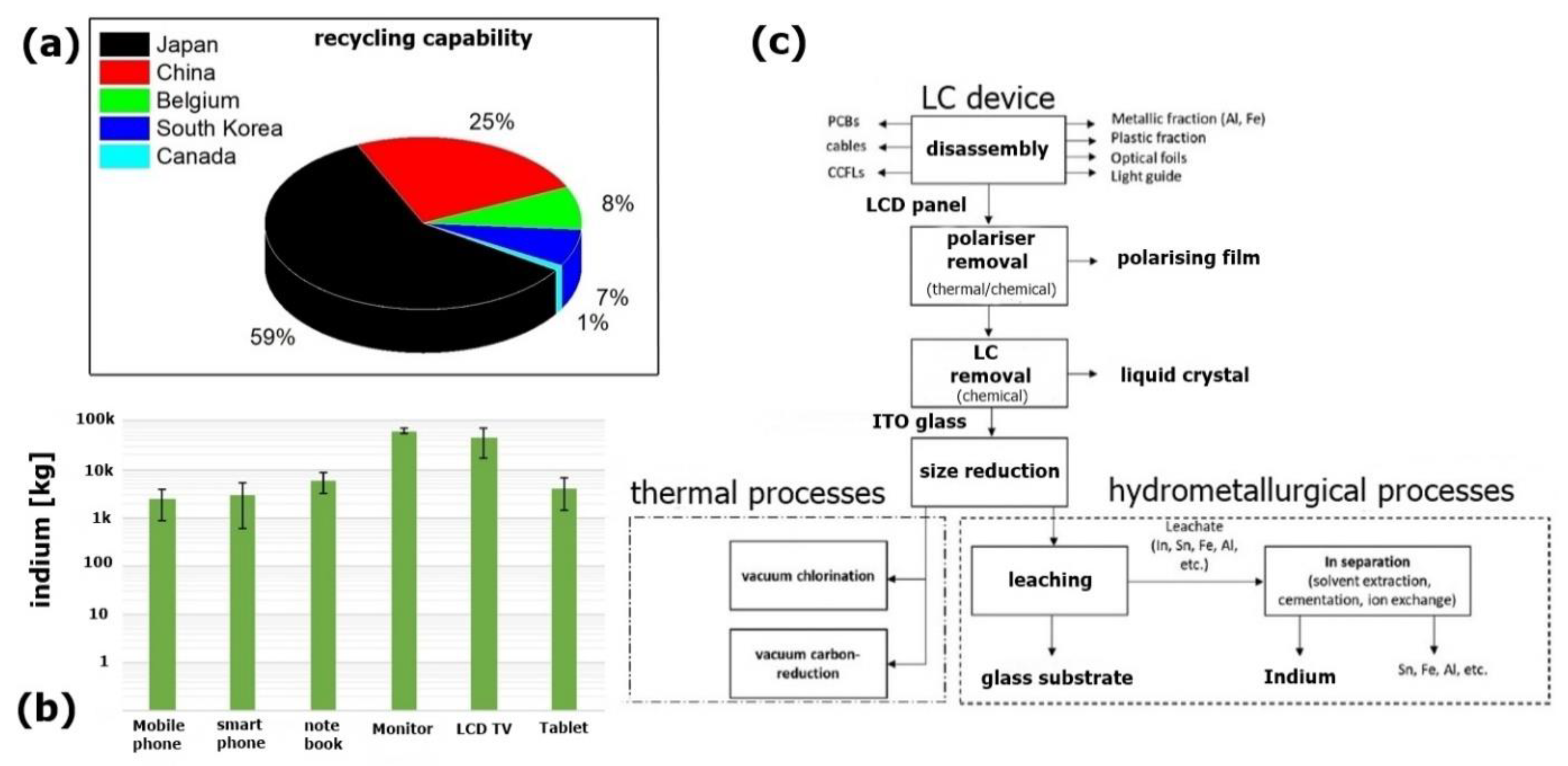
Currently, the country with the largest recycling capability of indium (secondary production mainly from waste products during manufacturing) is Japan, followed by China, Belgium, and South Korea (Figure 3a) [5]. Naturally, the largest amount of indium is recycled from liquid crystal display (LCD) TVs and computer monitors, while tablets, smartphones, and mobile phones play a much less significant role. This is due to the obviously much smaller display size of the product, but also because these devices are often not simply disposed of, but often kept in cupboards. The overall amount of indium recycled from end-of-life display devices is of the order of 80 tons, representing approximately 10% of the secondary indium production [8]. The amount of indium retrieved from one ton of electronic display waste varies between about 100 and 1400 g, depending on respective device products and treatment methods [9].
A typical recycling process is schematically depicted in Figure 3c. It starts with the collection of end-of-life liquid crystal display devices, which are then manually disassembled into a number of different fractions, including plastic housing, metal pieces, cables, printed circuit boards (PCB), cold cathode fluorescent lamps (CCFL) of the backlight, optical foils, and light guides. Once disassembled, the polariser from the actual LCD panel is often removed by thermal [11] or chemical methods [12]. In some processes, polariser foils are also recovered after a thermal shock treatment [13]. Then, the liquid crystal (LC) is removed in a chemical process, generally by dissolution with an organic solvent. This leaves the ITO-covered glass, which needs to be mechanically crushed and milled to reduce the size to a powder of approximately 10–20 μm grain size [14]. Different milling processes can be employed, leading to variations in indium recovery efficiency. To separate the ITO and therefore indium from the glass, two principle process may be employed: a thermal process and the more widely researched hydrometallurgical processes. The former consists of vacuum chlorination [15] or vacuum carbon reduction [16], while the latter uses leaching with mainly HCl, H2SO4, or HNO3 [11,17] to separate the glass from the leachate, which contains different metals such as In, Se, Fe, and Al. Then, these are further separated by solvent extraction [18,19] or cementation [20].
The topic of indium recycling, different strategies and applied methods, is obviously too extended to be treated comprehensively in this review, which is rather concerned about the possible replacement methodologies of ITO in the liquid crystal technology sector based on carbon allotropes. Thus, we refer the interested reader to some excellent reviews on the aspects of indium recycling. A first summary of the recovery of valuable materials from waste liquid crystal display panels has been given by Li et al. [21] already more than a decade ago. A more recent review of recycling indium from waste LCDs was published by Zhang et al. [22]. The recent advances of indium metallurgy were reviewed by Pradhan and co-workers [23], with a particular view on comparing mining and secondary indium production from LCDs. The potential and strategies for recycling LCDs was discussed by Ueberschaar et al. [8], while a very recent review with a particular focus on indium was published by Fontana et al. [10]. An enlightening analysis of the techno-economic aspects of waste LCDs as a source of value for electronic waste treatment centres can be found in a work by D’Adamo et al. [24], while Amato and Beolchini [25] provide a recent patent review for recycling of end-of-life liquid crystal displays.
2. Non-Carbon ITO Replacement Technologies
Above, we have shortly discussed indium (In) and indium tin oxide (ITO), as well as some recycling aspects of that critical metal, because ITO is still the by far most used material for transparent electrodes, not only in liquid crystal display (LCD) technology, although this makes up most of its global use. There are several reasons behind this fact. Firstly, it simply is the major established technology in industry, which is reluctant to change when devices work perfectly fine. With a resistivity of approximately 10–30 Ω□−1 for a film of approximately 200 nm thickness and a transmission of >90% for optical wavelengths, ITO outperforms most of its rivals. Secondly, its properties rival most replacement methods with respect to transmission, which is a key factor in display devices. A third reason is its environmental stability against degradation. LCDs based on liquid crystal-filled ITO sandwich cells or panels are UV stable and can last for several decades. Nevertheless, the use of ITO also has its drawbacks. The first lies in the production process of ITO coated glass, which is based on sputtering techniques. These are slow in production and relatively expensive due to losses and the high temperatures and vacuum equipment needed. Solution-based processes as used for other transparent electrode materials are much faster and mostly cheaper. Another disadvantage of ITO is a certain brittleness, which makes other materials better suited for flexible substrates, which is a display development that is predicted to strongly increase in the future. For these reasons, as well as the discussed limited natural resources of indium, a range of other materials are currently developed for the use as flexible, transparent electrodes. These include doped metal oxides other than ITO, metal grids, silver nanowires and meshes, conductive polymers, ultrathin metal films, carbon nanotube films and graphene, as reviewed by Cao and co-workers in reference [26]. In the following, we will shortly introduce some of these materials before concentrating in more detail on the carbon allotropes as well as carbon-based composites.
2.1. Metal Nanowires
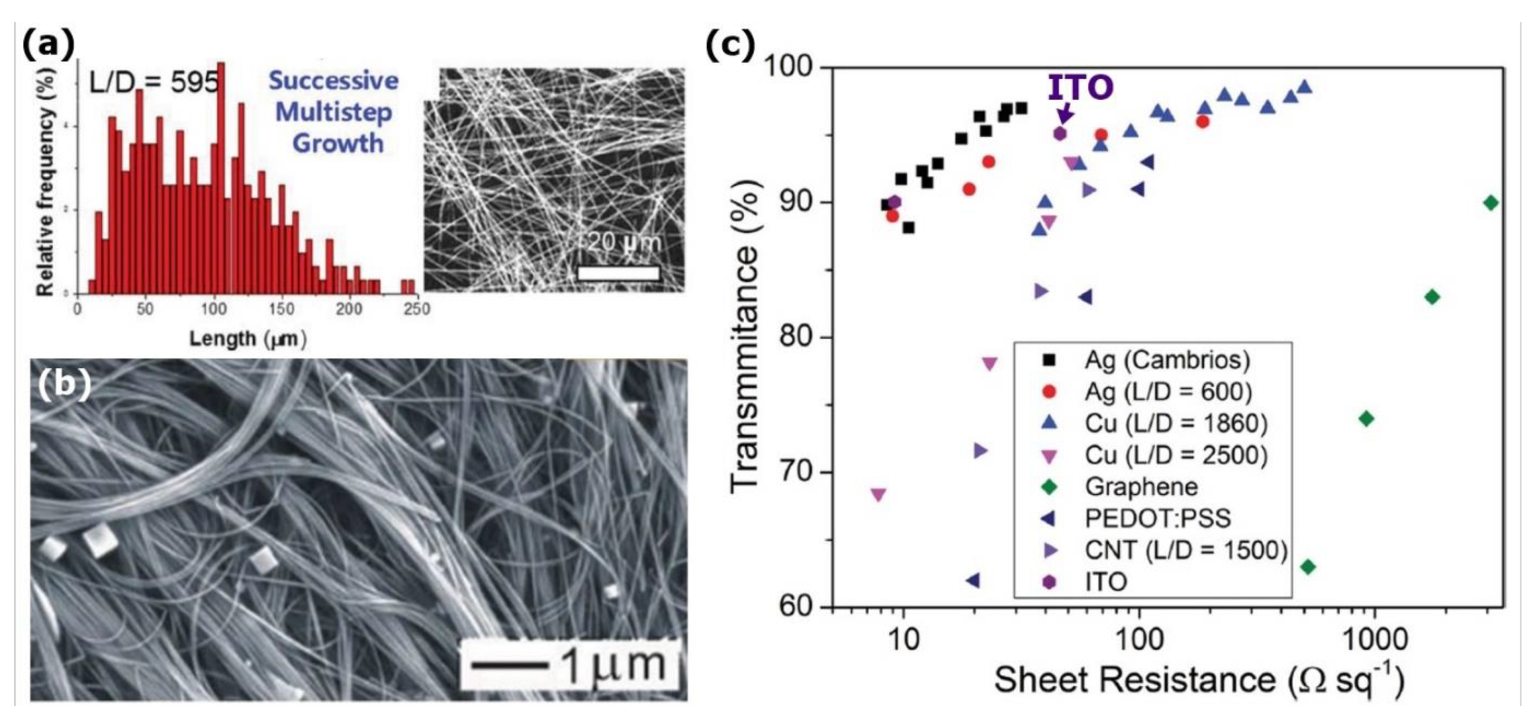
One of the most promising materials that may be used to replace ITO as transparent electrodes in future technologies are most likely meshes or thin films of metal nanowire networks [27,28]. Two different metals are commonly used, Cu [29,30], and the even more popular Ag nanowires [31,32,33,34,35,36,37,38,39,40], due to their very high conductivity. A comparative study of yet another few materials used (Cu, Ag, Al, and Au) can be found in reference [41].
The metal nanowires have a quite polydisperse length of the order of 100 μm and are very thin with a diameter of approximately ≈20 nm (Figure 4). One of the main advantages of nanowires is their processing possibilities, which includes solution processing and electro-spinning, which makes them most suitable for flexible polymer substrates. They can be produced as random thin film networks, meshes, and oriented structures, which can also be aligned.
With respect to performance as transparent electrode material, the main parameters are sheet resistance R, which should be low, and transmittance T, which should be high. The industry standard for ITO is approximately R ≈10 Ω□−1 and T ≈ 93%. As can be seen from Figure 4c, silver nanowire electrodes achieve a similar performance as ITO, while copper nanowires lag behind in sheet resistance for the required transmittance, or alternatively, if they achieve the required sheet resistance, the transmittance strongly decreases to values not acceptable or optical applications, such as liquid crystal displays. Currently, it appears that the only real alternative to ITO with regard to the physical performance side is Ag nanowires, which also explains why the main effort in metal nanowire research lies on these materials, as is evidenced in the number of review articles specifically written about silver nanowires. Langley et al. [44] have reviewed the fabrication, properties of Ag nanowires, and applications employing the latter as electrode material. Two much more recent summaries of the current state-of-the-art with respect to Ag nanowire networks have been written by Dongchen Tan et al. [45] and by Wenting Li et al. [46].
2.2. Conductive Polymers, PEDOT:PSS
Of all the conductive polymers [47,48], it is poly(3,4-ethylenedioxythiophene) (PEDOT) and its additive poly(styrene sulfonate) (PSS), which form the transparent, conductive polyelectrolyte complex PEDOT:PSS [49,50,51,52,53,54,55], which are by far the most prominent to be used as electrode materials. The chemical structure of PEDOT:PSS is shown in Figure 5a, together with a schematic representation of the polymer film formed from gel particles in dispersion with water. The grey areas of the film are PSS rich, while the blue areas are PEDOT: PSS rich, with crystalline regions that enhance the conductivity.
The performance of PEDOT:PSS as an electrode material in comparison to ITO reveals that the transmittance of up to T ≈95% can in fact be similar to that of ITO, while the sheet resistance is usually substantially larger, in the order of several 100 Ω□−1. As with most of the electrode materials, transmittance versus sheet resistance is a trade-off in performance. For PEDOT:PSS with a sheet resistance comparable to that of poor ITO (R ≈60 Ω□−1), the transmittance reduces to below 80%, which is not acceptable for high-performance liquid crystal devices.
Nevertheless, some liquid crystal applications have been demonstrated in which the ITO electrodes were replaced by PEDOT:PSS. These were mainly applications where solution processing is desirable, for example in devices with flexible substrates. One of such applications is polymer-dispersed liquid crystals (PDLC), where liquid crystalline droplets are dispersed in a polymer matrix. These devices switch from a scattering mode at zero-applied electric field to a clear, transmissive mode for applied voltages. An exemplary device was presented with post-treated PEDOT:PSS electrodes [58], where it was shown that the electro-optic performance was comparable to that with ITO electrodes. Similarly, such a technology has been used to demonstrate privacy windows on the basis of electrodes combining Ag nanowires with PEDOT:PSS, which exhibited a performance slightly diminished to that using ITO electrodes [59]. A different application of PEDOT:PSS electrodes are flexible liquid crystal contact lenses with a variable focal length [60]. However, also, more traditional display designs were accomplished with PEDOT:PSS electrodes, a normal twisted nematic (TN) cell [57], vertically aligned nematic (VAN) cells [61], or TN devices for phase shifters in the THz frequency regime [62].
2.3. Ultrathin Metal Films
Another alternative to the use of ITO as electrode materials that has been proposed is to employ metals of larger availability, for example silver, gold, copper, or aluminium, as ultrathin layered transparent films [67,68]. One of the problems with the production of ultrathin metal layers, which exhibit a thickness of approximately 3–10 nm, is the growth of islands [69,70], which is shown in Figure 6a for an ultrathin silver film. This leads to a percolation threshold behaviour for the conductivity (and thus sheet resistance). This island growth may be reduced or even avoided through the addition of seed layers [71,72,73,74,75,76,77,78], which are often Ge, TiO2, Al, Au, Cr, or Ni.
The wetting behaviour of the metal on the substrate is one of the key factors for reducing the percolation threshold, as well as the surface roughness [80]. Seed layers of thickness 1–2 nm [81] and doping [82,83,84,85] of the ultrathin metal films often with Al, N, or O, are the main parameters to adjust the wetting behaviour.
Figure 6b summarises the T-R performance of a collection of data on ultrathin metal films of Ag, Au, and Cu, produced by a variety of methods including seed layers and doping. The data can be found in tabular form in the excellent recent review on ultrathin metal films as transparent electrodes by Yan-Gang et al. [86]. From the graph, it is apparent that ultrathin metal films can outperform ITO in terms of sheet resistance, which can be decreased to well below 10–20 Ω□−1. Problems in the replacement of ITO electrodes are related to the transmittance values, which are quite clearly below 90% in nearly all cases, representing the barrier threshold for any electrooptic applications utilising liquid crystal technology. Furthermore, besides the optical performance, also the production process of ultrathin metal films represents no strategic improvement over standard ITO electrodes, as discussed in the review by Yun [87].
3. Carbon Allotropes as Electrode Materials
Due to the possibility of large conductivities and charge mobility, carbon nanotubes as well as graphene have been discussed as potential materials for transparent electrodes for a number of years [88,89,90]. The clear advantage of these materials over ITO, but also other methods such as ultrathin metal films, lies in the possibility for solution processing, which enables the production of flexible electronics and displays in conjunction with polymer substrates. One of the problems is the poor solubility, which has partially been resolved by the use of surfactants [91,92]. On the other hand, this use of surfactants or even covalent bonding of dispersion agents negatively affects the conductivity. Nevertheless, in recent years, some enhanced solutions have emerged.
3.1. Single-Wall and Multi-Wall Carbon Nanotubes
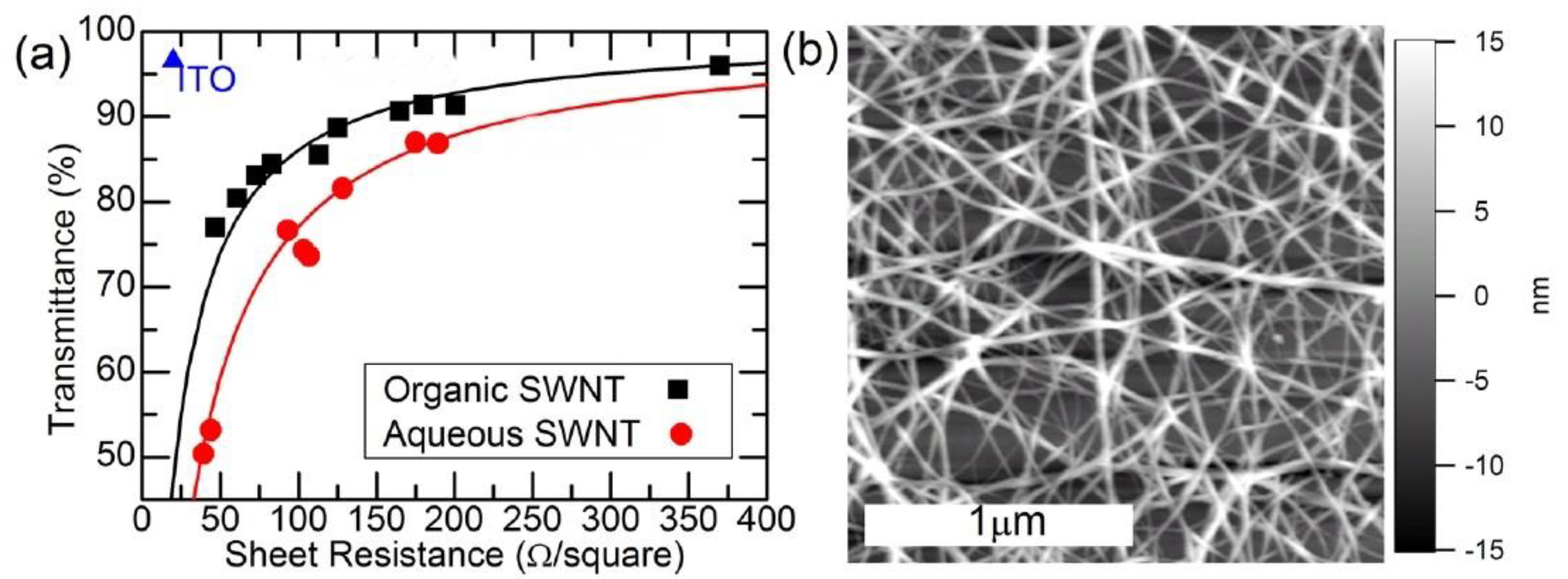
The main issue of using carbon nanotubes as materials to form thin network sheets as transparent electrodes is again the trade-off between transmittance at optical wavelengths and sheet resistance [93,94,95,96,97,98,99], as shown in Figure 7 [100].
Due to the poor interconnectivity between nanotubes and nanotube bundles in the film, the sheet resistance is increased. Surfactants or dispersing agents further reduce the conductivity and thus increase the sheet resistance. The sheet or network conductivity can be described by a percolation mechanism [36,101], which already indicates that poor interconnectivity between carbon nanotubes is one of the major problems, and that an understanding of the conductivity mechanism involves a fragile balance between carbon nanotube quality, solubility, dispersion agent, and processing conditions. This is essential for a reproducible and thus commercially viable source of carbon nanotube network films for transparent electrodes. Further, the sheet resistance of those electrodes at approximately R > 200 Ω□−1 for acceptable transmittance values of T > 90% is still too large. Any solution based on carbon nanotubes alone, which reduces the sheet resistance, decreases the transmittance to unacceptable values (Figure 7a). A further problem, specifically also with respect to liquid crystal applications, is the roughness of the carbon nanotube films (Figure 7b). These issues of interconnectivity and roughness have been addressed by post-treatment with strong acids, such as HNO3 [102].
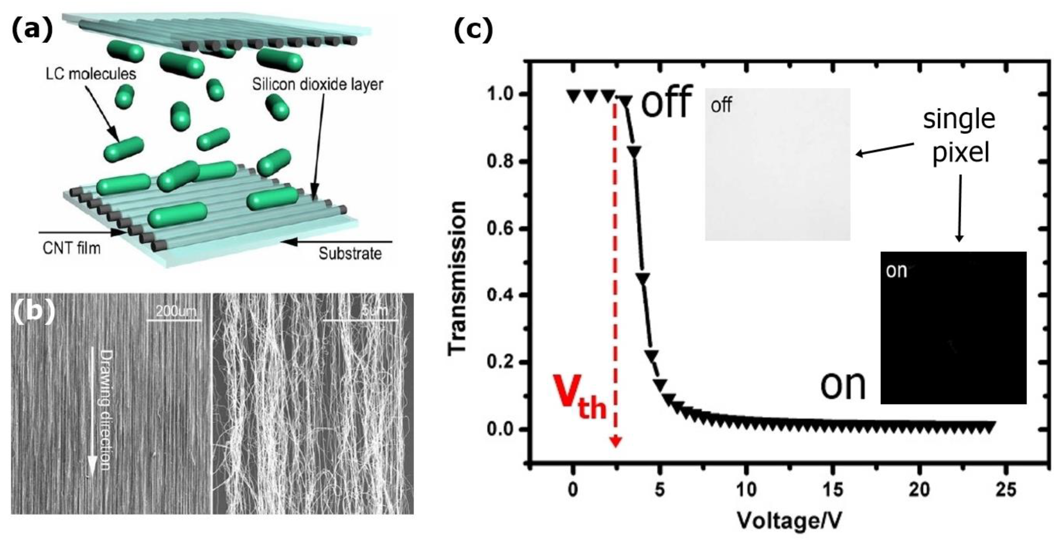
Thin nanotube network films [103,104,105,106] and treated films for increased conductivity [107,108,109] may be used as electrodes for liquid crystal devices. In addition to the feature of acting as an electrode, one would like to incorporate further functionality, for example, the action as a patterned substrate [103] or an alignment layer [110,111,112]. Most often, this would be a planar alignment of the liquid crystal, for example, in a TN cell, as shown in Figure 8a. This can be achieved by aligned nanotubes or nanotube bundles, which are depicted at different magnifications in Figure 8b. The liquid crystal molecules will align in such structures with their long molecular axis parallel to the natural grooves, which are otherwise generated through rubbing a polymer layer that is spin-coated onto the ITO electrode. In the case of the aligned nanotube films, the latter fulfils both functions at once: that of the electrode and that of the alignment layer.
For a TN cell, the orientation direction of both substrates is chosen such that the bottom and top alignment are at an angle of 90 degrees. Incoming linear polarised light is guided by the twisted structure and can pass the crossed polariser. The device appears transmissive, or bright without applied voltage, as shown in Figure 8c. Application of an electric field above the threshold causes the positively dielectric liquid crystal to reorient the long molecular axis, which is at the same time the optic axis, along the field direction, perpendicular to the substrates. Incoming linear polarised light is not affected by the LC and is absorbed by the crossed polariser. The device appears black. A typical transmission curve of a TN device as a function of applied voltage via the nanotube electrodes is also shown in Figure 8c. Although most often employed, not only single-wall carbon nanotubes (SWCNTs) can be used for applications as electrodes in liquid crystal devices, but also devices with multi-wall carbon nanotubes (MWCNTs) are feasible [113,114,115], albeit at even higher sheet resistance.
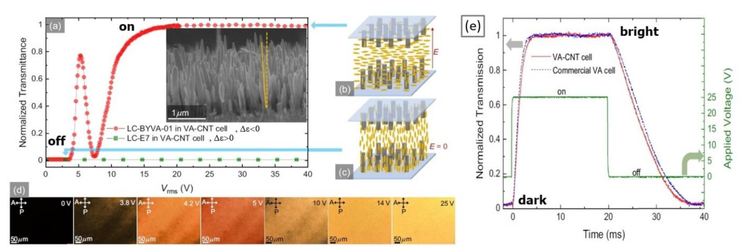
Similarly, it was very recently demonstrated that also a vertically aligned liquid crystal device can be constructed with nanotube electrodes and alignment [116]. Nanotubes are (nearly) vertically grown on the substrate, and the liquid crystal orients perpendicular with its long molecular axis to the substrates on both sides. Here, the long molecular axis represents the director and thus the optic axis. When viewed at zero applied voltage between two crossed polarisers, the device appears black in the off state, as there is no birefringence when the direction of light propagation is along the optic axis. Incoming linearly polarised light is unaffected by the LC and absorbed by the crossed polariser. In the case of such a vertically aligned cell, one employs a liquid crystal with a negative dielectric anisotropy. This will switch from homeotropic to planar for an applied voltage above a threshold voltage, leading to an electro-optic response of the cell, as shown in Figure 9a. The corresponding schematic device with nanotube alignment electrodes (grey) and liquid crystal orientation (yellow) is shown for the electric field on- and off-state in Figure 9b,c, respectively.
When viewing the device between crossed polarisers, one thus observes an increasing transmission from the dark off-state to the bright on-state, as the voltage across the cell is increased (Figure 9d). The dynamic response of this device is depicted in Figure 9e. The response time for the dark off- to the bright on-state is dependent on the applied electric field and of the order of a few milliseconds. That of the transition from the bright on- to the dark off-state is longer, as it is not driven by the electric field but dominated by elastic interactions between the liquid crystal and the homeotropic substrate. One should also note that the very slight offset angle of the nanotube alignment from the right angle to the substrate (Figure 9a) is in fact intentional and of great advantage, as it prevents the formation of so-called reverse tilt domains, which degrade the performance of any vertically aligned nematic LC device.
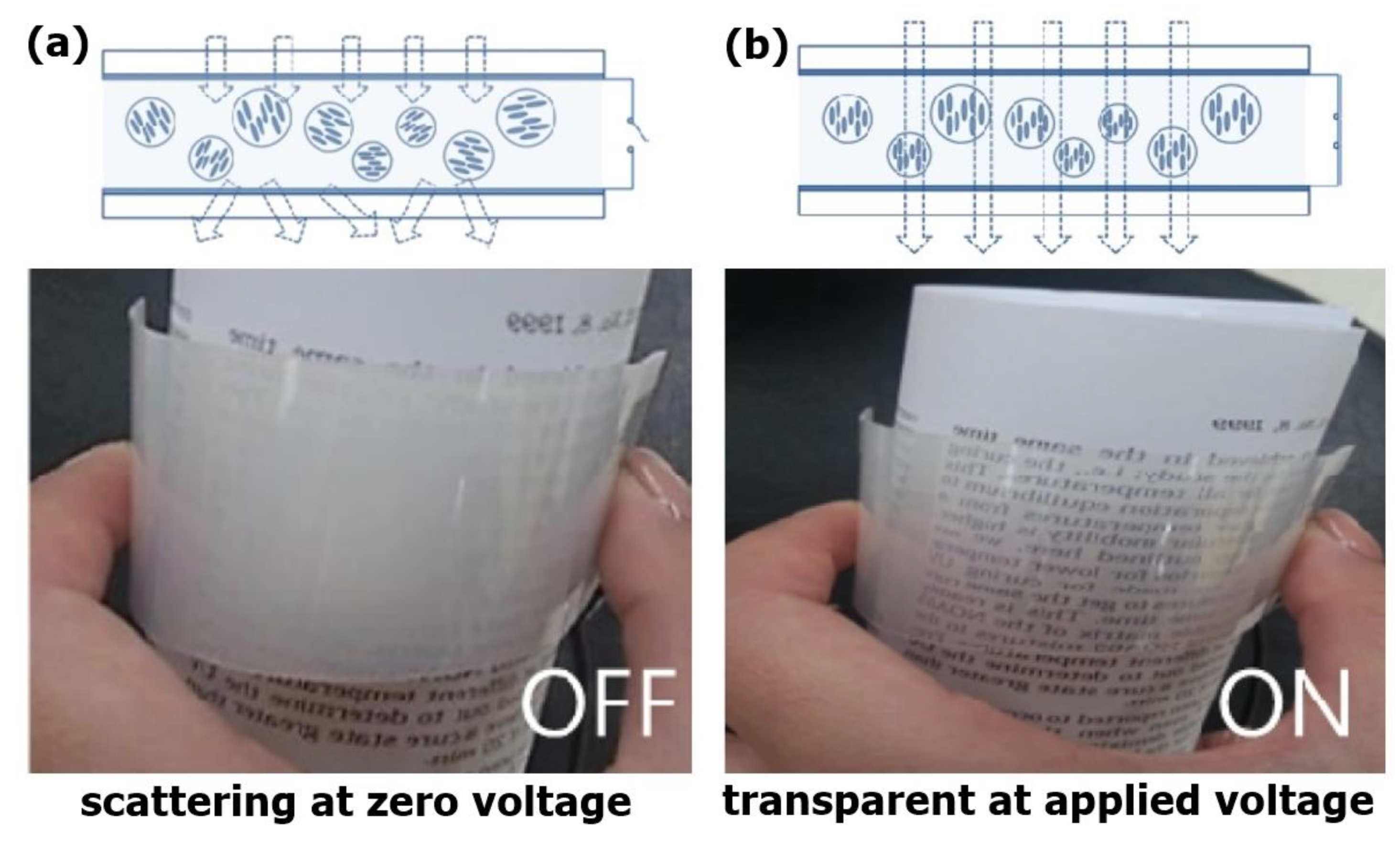
We should mention at this point that also other display devices based on liquid crystals have been realised with nanotube film electrodes, such as polymer-dispersed liquid crystals (PDLC) [117]. These are scattering devices without the use of polarisers. Liquid crystal droplets of the low micrometre-size range are dispersed and phase separated within a continuous polymer matrix. This leads to light scattering as the LC director is randomly oriented. Application of an electric field via nanotube film electrodes causes the director to align with the field direction. The refractive index of the surrounding polymer matrix is matched to that of the long molecular axis and scattering is diminished, the device becomes transparent. PDLCs have their application as privacy windows, and nanotube electrodes can be produced as flexible foils.
Other applications of conductive, transparent nanotube film electrodes in liquid crystal devices are mostly found as hybrid materials with other technologies, such as Ag nanowires, PEDOT:PSS, or graphene, and these will be discussed in more detail below. A review of the fabrication, properties, and applications of carbon nanotube thin films was published by Liangbing Hu et al. [118] and more recently by Hirotani and Ohno [119], concentrating on flexible electronics applications.
3.2. Graphene, Graphene Oxide, and Reduced Graphene Oxide
Due to its high electric conductivity, transparency, and mechanical stability, graphene and its derivatives appear to be ideal materials for transparent, ITO-free electrodes that offer solution processibility and the potential for flexible devices [120,121,122,123,124,125,126,127,128]. In principle, for single-layer graphene, a transmittance of T = 97.7% can be achieved with a sheet resistance of approximately R ≈ 30 Ω□−1. These are theoretical values that have very closely been reached experimentally under laboratory conditions [129,130,131,132]. Under more realistic conditions, on the other hand, for real graphene thin films, flake sizes imply that multi-layers may exist and that there are grain boundaries both affecting the transmittance and the sheet resistance. Therefore, as in the case of carbon nanotubes, there will be a trade-off between conductivity, transmittance, device lifetime, and cost [133,134].
Probably, the first LC device made with graphene electrode is a cell shown schematically in Figure 10a, consisting largely of graphene on a glass substrate, a polyvinyl alcohol alignment layer, and the nematic liquid crystal, which is covered by a top substrate with an ITO electrode [128]. The electro-optic response as a function of applied increasing voltage is shown in Figure 10b, switching the liquid crystal from a bright zero volt off-state to a dark on-state.
The transmission through the 20 μm thick LC device is shown in Figure 10c for monochromatic green light with a wavelength of 505 nm (blue curve), as well as for white light (red curve in the inset). The oscillatory behaviour of the transmission is due to the change in birefringence, as the molecular long axis reorients for increasing applied voltage, which results in an additional phase retardation of several multiples of π.
We have seen above that aligned nanotube films can be used not only as electrode material but simultaneously as an alignment layer for the liquid crystal. A similar behaviour can be observed for graphene due to the π–π interaction of the carbon honeycomb lattice with the phenyl-ring system of the liquid crystal core. This has been exploited in nematic devices [135,136] as well as a ferroelectric liquid crystal (FLC) cell with graphene electrodes and alignment [137].
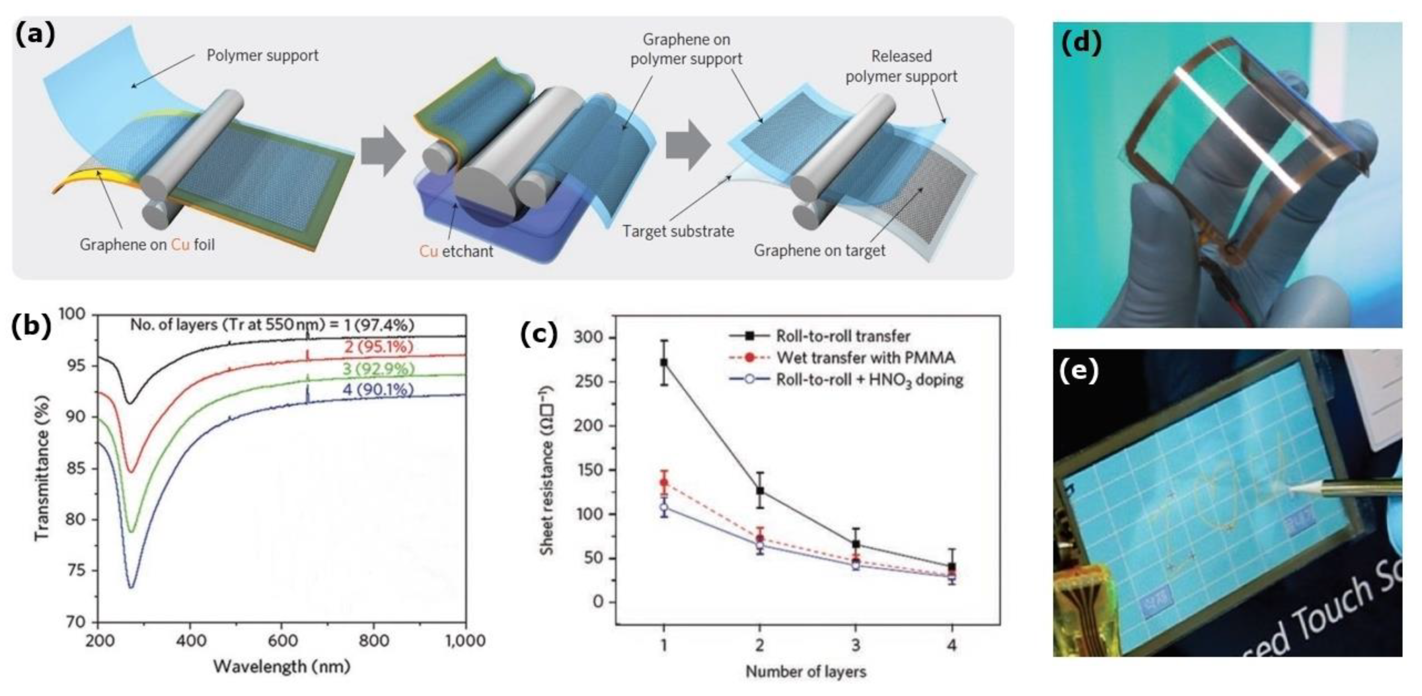
Another advantage of graphene electrodes is the possibility to produce flexible substrates on polymer films, as shown in Figure 11. The graphene film is grown on a copper foil, which is laminated to the polymer film. In an etching step, the copper is removed, and the flexible graphene on polymer foil electrode is obtained. This has been shown to produce flexible substrates of sizes up to 30 inches [121], but it may be extended to even larger sizes, which is suitable for example for the use in the production of touch screen displays or PDLC privacy windows. The process can be repeated for a layer by layer increase of the graphene film. The successive addition of graphene layers reduces the transmittance in the optical wavelength regime (Figure 11b), while it decreases the sheet resistance (Figure 11c). Once again, a compromise needs to be made between high transmittance and low sheet resistance, although for 3-layer substrates, the performance comes close to that of ITO, with the additional benefit of flexibility, as shown in Figure 11d or the touch panel of Figure 11e.
Other applications of ITO-free, flexible, and transparent graphene electrode liquid crystal devices can be found in the previously discussed Polymer-Dispersed Liquid Crystals (PDLC) for example as privacy or smart windows [138,139]. These will be discussed further in Section 4.
Furthermore, to reduce costs, it has also been attempted to exploit reduced graphene oxide (rGO) as electrode material [140,141,142,143,144]. This can be obtained from graphene oxide (GO) through thermal reduction, i.e., heating to approximately 160 °C, when GO loses its surface and edge attached epoxide and hydroxide functional groups. While GO is non-conducting, rGO regains some of the conductivity of graphene. It should be noted though that the sheet resistance of rGO films is much larger than that of graphene or indeed ITO, at values of approximately RrGO≈1–50 kΩ□−1. In addition, the transmittance is generally not quite acceptable for high-end display applications, ranging at about TrGO ≈ 80%. This performance can be somewhat improved by acid treatments [145] or the doping and attachment of Ag nanoparticles [146].
As in the case for carbon nanotubes, much research is being done to increase the performance of graphene or graphene-based materials as electrodes, which are to be exploited effectively for electro-optic and flexible electronic devices. Here, one may resort to hybrid materials with PEDOT:PSS or silver nanowires or even nanotube/graphene hybrids for improvement, as will be discussed in more detail in the next section. Several reviews can be found on the topic of graphene-related materials as transparent, flexible electrodes, discussing different systems, preparation, and applications in detail [147,148,149,150].
4. Carbon Composite Technologies
From the discussion of many of the options to replace ITO by other materials, we have so far concentrated our attention on the use of single materials, such as metal nanowires, conductive polymers, ultrathin metal film, and especially carbon nanotubes and graphene. While there are materials with properties approaching those of ITO in terms of high transmittance and low sheet resistivity, there is no competitor that is clearly standing out. Thus, one can try to combine the various advantages of different approaches in such a way that the shortcomings of one material may be compensated by another through hybrid approaches or composite materials. In the following, we will focus on composites incorporating carbon allotropes.
4.1. Nanotube-Based Composites
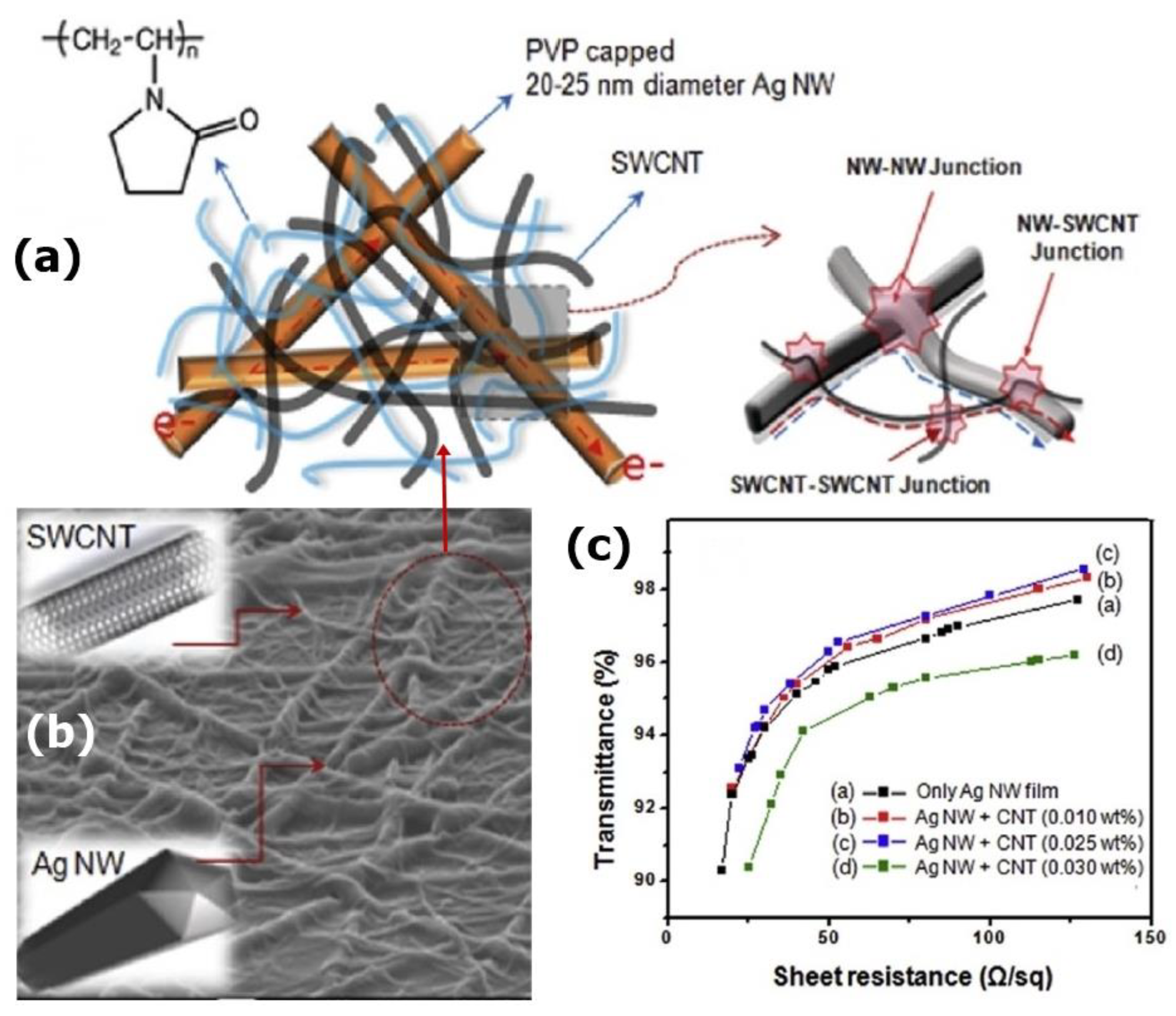
One of the popular combinations is that of metal nanowires with carbon nanotubes [151,152,153]. An example is shown in Figure 12, where a network of silver nanowires (Ag NW) forms a composite with single-wall carbon nanotubes to make a transparent conducting film [152]. The actual current conduction is achieved via different junctions, nanowire–nanowire, nanowire–nanotube, and nanotube–nanotube junctions, while the composite network is embedded in a polymer matrix.
The sheet resistance of the composite at equal transmittance values is lower than that of the Ag nanowire network alone due to the additional contact junctions formed by the carbon nanotube network. The electrode performance with a transmittance of 95% at a sheet resistance of 30 Ω□−1 is comparable to that of standard ITO electrodes, while showing the excellent bending behaviour needed for flexible devices. Similar results are shown by solution-processed carbon nanotubes with self-assembled Ag nanoparticles, which form a conductive nanoparticle network with sheet resistance < 10 Ω□−1 and transmittance of 84% [151]. Shin et al. [153] investigated the composites of an Ag metal grid in combination with multi-wall carbon nanotube (MWCNT) networks as well as graphene films. They found that while the transmittance was acceptable in all cases of possible combinations, (i) MWCNT, (ii) MWCNT + Ag grid, (iii) graphene, (iv) graphene + Ag grid, and comparable to that of ITO (93%), the sheet resistance was clearly larger in cases (i)–(iii) and only comparable to ITO (21 Ω□−1)for the graphene film with an Ag grid composite.
In addition, all-carbon composites of nanotubes and graphene-based materials have been produced. Double-layer composites of a MWCNT film on rGO [154] showed a drastic reduction of sheet resistance when the nanotubes were added onto the reduced graphene oxide film from about 30 to 2 kΩ□−1 before annealing. Even after annealing, the sheet resistance was still reduced by another factor of about 2 or 3. The transmittance was obviously also reduced as compared to single material solutions, but it remained at values > 90%, which is sufficient for devices. Similar attempts with multi-layer composites [155] produced electrodes with a transmittance of 81% and sheet resistance of 8 kΩ□−1. In addition, the use of nanotube interlinked graphene films [156] did not reach a performance that could rival ITO.
A possibility to increase the performance of nanotube-based composite electrodes is to embed the composite in a conductive polymer, mostly PEDOT:PSS [157,158,159,160]. Cho et al. [157] used multi-wall carbon nanotube networks for which the sheet resistance was reduced by the addition of gold nanoparticles anchored uniformly on the outside of the nanotubes. In a plasma treatment step, these nanoparticles fused individual MWCNTs to form conductive junctions and thus increase the percolation conductivity, leading to a reduction in sheet resistance of the network from approximately 225 to 50 Ω□−1, which is a value close to that of ITO (Figure 13). The such connected nanotube network was embedded in a PEDOT:PSS matrix. Together with a transmittance close to 90%, flexible transparent electrodes were produced, which had a much-improved bending behaviour compared to that of ITO electrodes. A similar methodology was used by Shin et al. [158] to achieve a corresponding performance. Furthermore, hybrid composites combining rGO, MWCNTs, and PEDOT:PSS were realised [159], as well as Ag nanowire–nanotube–PEDOT:PSS hybrids [160] with 86% transmittance and sheet resistance as low as 7 Ω□−1.
4.2. Graphene-Based Composites
Most single graphene material approaches show that the transmittance of a one to four-layer graphene film lies above approximately 90%, which is comparable to ITO. Yet, due to the relatively small graphene flake sizes, there are numerous defects and grain boundaries in such films, which increase the sheet resistance to values far above those observed for the standard ITO material. This implies that a hybrid approach is favourable, and as for carbon nanotube films, also for the use of graphene in electrode materials, the most investigated composite appears to be a hybrid structure of metal nanowires with graphene-based films [161,162,163,164,165,166].
Chen and co-workers [161] proposed a co-percolating graphene–Ag nanowire structure in two different hybrid varieties: (1) Ag nanowire network on a flat film of graphene and (2) Ag nanowire network covered by a graphene film. While in both cases, the sheet resistance of the hybrid is strongly reduced from that of a graphene film alone, it is still not competitive with ITO for hybrid-1. On the other hand, hybrid-2 does exhibit a sheet resistance of about 20 Ω□−1 at a transmittance of approximately 90%. These are values as expected for good ITO electrodes. Given the relatively costly price of silver and the very much comparable conductivity of copper at much lower costs, it is well worth exploring the possibility of replacing the Ag nanowire with a Cu nanowire network [162]. Such a Cu nanowire–graphene hybrid electrode was shown to have a sheet resistance of ≈ 50 Ω□−1 at a transmittance of ≈ 90%, which is still quite close to the performance of ITO. A similar electrode hybrid with Cu nanowires has also been proposed using reduced graphene oxide, rGO, albeit at increased sheet resistance of 300 Ω□−1 for a 90% transmittance [164]. A hybrid Ag nanowire–GO electrode has been demonstrated to drive a PDLC display [165].
A somewhat different fabrication approach was chosen by Liu et al. [166], in depositing an Ag nanowire–graphene hybrid material on flexible polymer (PET) substrates through electrophoresis, as shown in the scheme of Figure 14. The transmittance of the reported device is practically constant over the optical range of the visible spectrum, and it depends on the applied electrophoresis voltage, decreasing with increasing voltage amplitude, and generally being still too low at T < 65% for high-end optical technology. On the other hand, the sheet resistance is in fact well below the normally required values for ITO-free electrodes.
Another approach that we have briefly touched upon above is the combination of graphene and nanotubes in all-carbon based flexible and transparent electrodes [155,167]. It should be mentioned from the beginning that the performance of such electrodes with respect to sheet resistance is by no standards comparable to ITO—rather in the kΩ□−1 than the low Ω□−1 range and thus far larger than desired by the liquid crystal display industry. Nevertheless, it is worthwhile to discuss these approaches because of the excellent flexibility, bending behaviour, processing, and lower costs of these hybrid materials. Furthermore, these graphene-based composites can in fact be made from the largely available graphene oxide or reduced graphene oxide. Figure 15 depicts one of such electrodes composed from multi-layer GO/rGO and MWCNTs.
By atomic force microscopy (AFM), one can clearly resolve the surface morphology of the multi-layer GO/rGO-MWCNT structures with GO/rGO flakes visible at an average size of approximately 1 μm and MWCNTs on top, leading to a surface roughness of about 10 nm on average. The latter strongly increase the conductivity, or lowers the sheet resistance, by bridging the grain boundaries and possible open spaces of the GO/rGO layers. Nevertheless, even after treatment procedures to further decrease the sheet resistance, the latter is still well in the kΩ□−1 range, much larger than for ITO and indeed other single material or hybrid electrode materials. While the transmittance is high at about 95% for small numbers of bilayers, it naturally continuously decreases with increasing the number of bilayers.
5. Applications of Carbon-Based ITO-Free Technologies
We have discussed the possible need for replacement technologies of ITO electrodes, not simply in light of the limited supply of indium, but also due to reasons of an increasing need for flexible substrate technologies, which require different processing conditions. Several materials were shown to be candidates for a sufficiently transparent yet highly conductive ITO-free technology, including hybrid materials and composites. We will now specifically address some of the applications based on liquid crystals that incorporate these ITO-free electrodes, besides the already mentioned twisted nematic TN cells [103,136] or the vertically aligned switching devices with negative dielectric liquid crystal [116].
One of the promising ITO-free applications are flexible privacy windows, as demonstrated in Figure 16 [138]. Sub-micrometre nematic droplets are dispersed in a continuous polymer matrix with graphene electrodes for electric field application. In the electric field free off-state, the film is strongly light scattering, due to a random orientation of director field of the LC droplets, which leads to an abruptly changing refractive index on length scales of optical wavelengths (Figure 16a). The application of an electric field causes a director reorientation of the LC within the droplet such that the long molecular axes are all pointing in the same direction. Light experiences a refractive index n‖, which is index matched to that of the isotropic polymer matrix, npolymer≈n‖, and the foil becomes transparent (Figure 16b). It is worth noting that these foils rely on light scattering, not on the modulation of the polarisation state of light, and thus, they do not have any need for polarisers, which generally absorb a lot of the transmitted light intensity already. A similar device was also demonstrated by Kim et al. [139].
THz devices have increasingly become important in the area of non-destructive testing and for security screening. As liquid crystals are switchable and thus are suitable to modulate the birefringence of devices also in the THz regime, it is of benefit to construct LC-based THz optical components. One of the problems is the opaqueness of ITO at these frequencies, which cause the need for THz-transparent electrodes. A number of phase shift and wave-plate devices have been reported, which utilise graphene film electrodes.
Such ITO-free LC devices are for example employed as THz phase shifters [168] and polarisation phase controllers [169], THz quarter wave-plates [170], or broadband tuneable liquid crystal THz wave-plates [171]. Figure 17a schematically depicts such a THz device, which resembles a liquid crystal sandwich cell with planar boundary conditions and graphene electrodes. The application of an electric field switches the dielectrically positive liquid crystal from planar to homeotropic orientation, changing the THz refractive index. For the graphene electrodes, one is once again faced with the compromise between transmittance and sheet resistance. Ideally, the device would have a high transmittance > 90% while exhibiting a low sheet resistance < 50 Ω□−1. A suitable compromise would probably be a two-layer graphene film. The THz signal that is transmitted through the device is phase shifted depending on the applied voltage, as shown for several different applied voltages and frequencies in Figure 17d,e, respectively.
For all non-display LC devices that rely on curved, flexible surfaces, an ITO-free electrode on a polymer substrate is of great advantage. An illustrative example of such a device is switchable lenses and variable focus lenses and especially adaptive contact lenses [60,172,173].
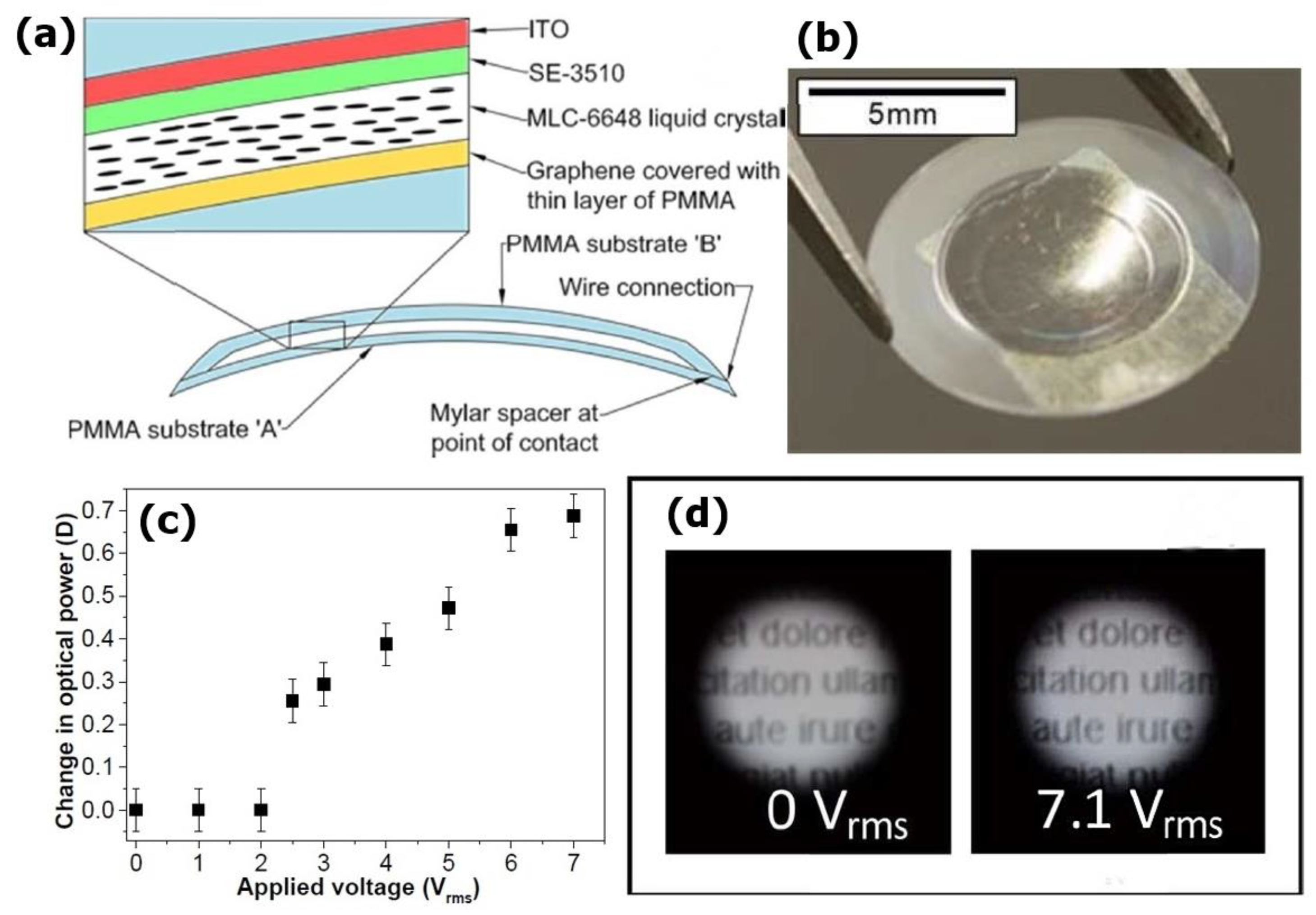
An example of a contact lens of size suitable for the human eye is depicted in Figure 18, which is based on a flexible polymer substrate and covered with a transparent graphene electrode on the curved active part of the contact lens. Above a threshold voltage of approximately 2 V, the optical power changes continuously up to 0.7 D, which allows focussing on a text.
6. Discussion and Outlook
In the last few years, it has emerged that the predicted shortage of indium to produce ITO electrodes on substrates is not as imminent as it was once feared. It now looks as though natural resources will last for the next three decades until about 2050. The price of indium has not exploded; on the contrary, it remained on a more or less constant level for a decade, despite the strong increase of flat panel display production during this time. One of the reasons is an increased indium recovery during the ITO sputtering process, where much of the material is in fact not being used up on the substrate. Furthermore, it can be expected that more indium will be recovered from advancing recycling processes. These will be not so much driven through the lack of indium resources but rather through ecological considerations, as an increasing amount of electronic waste in landfill will bring about advanced technologies for recycling not only of indium, but also glass, plastics, metal, and electronic components of end-of-life LCDs. At present, these technologies are not financially viable, and there will be the need for financial incentives, such as a blanket recycling fee for electronic consumable items, as it is already done in some countries.
Much research has been performed over the last decade to present technical alternatives to the use of ITO in displays and other optoelectronic applications. Some of these were outlined above, and the most promising appear to be based on Ag nanowire networks and meshes, graphene, and single-wall nanotube network films, and their composite materials. Materials are also available at comparable performance to ITO (Figure 19a), yet at still higher cost and mostly not having been scaled up to sizes and the reproducibility of industrial standard (Figure 19b). The main problem with all alternative material solutions appears to be the trade-off between high transmittance versus low sheet resistance. Nevertheless, it is well conceivable that these issues will be solved over the next few years.
Even once a performance equivalent replacement technology for ITO is found, it is unlikely that we will see ITO-free devices taking over the market soon afterwards. For this to happen, the new materials either need to be considerably better or clearly cheaper than ITO, because the latter is, and has been for many years, the established industry standard with all the necessary production infrastructure and R&D knowledge in place. Moreover, a deviation from this standard will be a slow process that can only be initiated via a considerable step-increase in performance or cost decrease, or for example via legislation in the form of environmental decisions, or with the development of novel display technologies, which cannot be realised with conventional ITO electrode techniques. One of such technologies that may be on the rise over the next years are flexible devices on polymer substrates, which cannot be processed by ITO sputtering techniques. In this case, solution processing would pave the way for electrodes either of metal nanowire networks or of carbon-based materials, or indeed composite materials of both. In this case, it is likely that price will be the decisive factor, which could favour carbon-based technologies. Especially, future large-area applications with environmental impact, such as energy saving or energy-harvesting windows, technologies which are often first seen on office buildings, could tip the balance towards carbon-based electrode materials. Yet, it is not likely that within the next few years, a drastic move towards ITO-free technologies will be observed.
Funding
This research received no external funding.
Conflicts of Interest
The author declares no conflict of interest.
References
- European Commission. Report on Critical Raw Materials for the EU: Report of the Ad hoc Working Group on Defining Critical Raw Materials May 2014, Ref. Ares(2015)1819503—29/04/2015. (See Also: European Commission, Critical Raw Materials for the EU: Report of the Ad-hoc Working Group on Defining Critical Raw Materials, June 2010.). Available online: https://ec.europa.eu/docsroom/documents/10010/attachments/1/translations/en/renditions/pdf (accessed on 14 November 2020).
- Nakashima, K.; Kumahara, Y. Effect of tin oxide dispersion on nodule formation in ITO sputtering. Vacuum 2002, 66, 221–226. [Google Scholar] [CrossRef]
- U.S. Geological Survey (USGS). Mineral Commodity Summaries 2019; U.S. Geological Survey: Reston, VA, USA, 2019. Available online: https://pubs.er.usgs.gov/publication/70202434 (accessed on 14 November 2020).
- Indium Statistics and Information. Available online: http://minerals.usgs.gov/minerals/pubs/commodity/indium/ (accessed on 14 November 2020).
- Lokanc, M.; Eggert, R.; Redlinger, M. The Availability of Indium: The Present, Medium Term, and Long Term, NREL, Report NREL/SR-6A20-62409, October 2015. Available online: https://www.nrel.gov/docs/fy16osti/62409.pdf (accessed on 14 November 2020).
- Hester, R.E.; Harrison, R.M. Analysis and Application, 2. In Electronic Waste Management Design; RSC Publishing: Cambridge, UK, 2009; Volume 27, p. 55. [Google Scholar]
- Stevenson, R. Endangered Elements. Phys. World 2020. Available online: http://physicsworld/a/endangered-elements/ (accessed on 14 November 2020).
- Ueberschaar, M.; Schlummer, M.; Jalalpoor, D.; Kaup, N.; Rotter, V.S. Potential and Recycling Strategies for LCD Panels from WEEE. Recycling 2017, 2, 7. [Google Scholar] [CrossRef] [Green Version]
- Zhang, S.; Ding, Y.; Liu, B.; Chang, C. Supply and demand of some critical metals and present status of their recycling in WEEE. Waste Manag. 2017, 65, 113–127. [Google Scholar] [CrossRef] [PubMed]
- Fontana, D.; Forte, F.; Pietrantonio, M.; Pucciarmati, S. Recent developments on recycling end-of-life flat panel displays: A comprehensive review focused on indium. Crit. Rev. Environ. Sci. Technol. 2020. [Google Scholar] [CrossRef]
- Fontana, D.; Forte, F.; De Carolis, R.; Grosso, M. Materials recovery from waste liquid crystal displays: A focus on indium. Waste Manag. 2015, 45, 325–333. [Google Scholar] [CrossRef] [PubMed] [Green Version]
- Silveira, A.V.M.; Fuchs, M.S.; Pinheiro, D.K.; Tanabe, E.H.; Bertuol, D.A. Recovery of indium from LCD screens of discarded cell phones. Waste Manag. 2015, 45, 334–342. [Google Scholar] [CrossRef]
- Savvilotidou, V.; Hahladakis, J.N.; Gidarakos, E. Leaching capacity of metals–metalloids and recovery of valuable materials from waste LCDs. Waste Manag. 2015, 45, 314–324. [Google Scholar] [CrossRef]
- Lee, C.-H.; Jeong, M.-K.; Kilicaslan, M.F.; Lee, J.-H.; Hong, H.-S.; Hong, S.-J. Recovery of indium from used LCD panel by a time efficient and environmentally sound method assisted HEBM. Waste Manag. 2013, 33, 730–734. [Google Scholar] [CrossRef]
- Ma, E.; Lu, R.; Xu, Z. An efficient rough vacuum-chlorinated separation method for the recovery of indium from waste liquid crystal display panels. Green Chem. 2012, 14, 3395. [Google Scholar] [CrossRef]
- He, Y.; Ma, E.; Xu, Z. Recycling indium from waste liquid crystal display panel by vacuum carbon-reduction. J. Hazard. Mater. 2014, 268, 185–190. [Google Scholar] [CrossRef]
- Swain, B.; Lee, C.G. Commercial indium recovery processes development from various e-(industry) waste through the insightful integration of valorization processes: A perspective. Waste Manag. 2019, 87, 597–611. [Google Scholar] [CrossRef] [PubMed]
- Virolainen, S.; Ibana, D.; Paatero, E. Recovery of indium from indium tin oxide by solvent extraction. Hydrometallurgy 2011, 107, 56–61. [Google Scholar] [CrossRef]
- Yang, J.; Retegan, T.; Ekberg, C. Indium recovery from discarded LCD panel glass by solvent extraction. Hydrometallurgy 2013, 137, 68–77. [Google Scholar] [CrossRef]
- Li, Y.; Liu, Z.; Li, Q.; Liu, Z.; Zeng, L. Recovery of indium from used indium-tin oxide (ITO) targets. Hydrometallurgy 2011, 105, 207–212. [Google Scholar] [CrossRef]
- Li, J.; Gao, S.; Duan, H.; Liu, L. Recovery of valuable materials from waste liquid crystal display panel. Waste Manag. 2009, 29, 2033–2039. [Google Scholar] [CrossRef] [PubMed]
- Zhanga, K.; Wua, Y.; Wanga, W.; Li, B.; Zhang, Y.; Zuo, T. Recycling indium from waste LCDs: A review. Resour. Conserv. Recycl. 2015, 104, 276–290. [Google Scholar] [CrossRef]
- Pradhana, D.; Pandab, S.; Sukla, L.B. Recent advances in indium metallurgy: A review. Miner. Process. Extr. Metall. Rev. 2018, 39, 167–180. [Google Scholar] [CrossRef]
- D’adamo, I.; Ferella, F.; Rosa, P. Wasted liquid crystal displays as a source of value for e-waste treatment centers: A techno-economic analysis. Curr. Opin. Green Sustain. Chem. 2019, 19, 37–44. [Google Scholar] [CrossRef]
- Amato, A.; Beolchini, F. End of life liquid crystal displays recycling: A patent review. J. Environ. Manag. 2018, 225, 1–9. [Google Scholar] [CrossRef]
- Cao, W.; Li, J.; Chen, H.; Xue, J. Transparent electrodes for organic optoelectronic devices: A review. J. Photonics Energy 2014, 4, 40990. [Google Scholar] [CrossRef]
- Ye, S.; Rathmell, A.R.; Chen, Z.; Stewart, I.E.; Wiley, B.J. Metal Nanowire Networks: The Next Generation of Transparent Conductors. Adv. Mater. 2014, 26, 6670–6687. [Google Scholar] [CrossRef]
- Sannicolo, T.; Lagrange, M.; Cabos, A.; Celle, C.; Simonato, J.-P.; Bellet, D. Metallic Nanowire-Based Transparent Electrodes for Next Generation Flexible Devices: A Review. Small 2016, 12, 6052–6075. [Google Scholar] [CrossRef]
- Kang, M.G.; Park, H.J.; Ahn, S.H.; Guo, L.J. Transparent Cu nanowire mesh electrode on flexible substrates fabricated by transfer printing and its application in organic solar cells. Sol. Energy Mater. Sol. Cells 2010, 94, 1179–1184. [Google Scholar] [CrossRef]
- Wu, H.; Hu, L.; Rowell, M.W.; Kong, D.; Cha, J.J.; McDonough, J.R.; Zhu, J.; Yang, Y.; McGehee, M.D.; Cui, Y. Electrospun Metal Nanofiber Webs as High-Performance Transparent Electrode. Nano Lett. 2010, 10, 4242–4248. [Google Scholar] [CrossRef]
- Xu, F.; Zhu, Y. Highly Conductive and Stretchable Silver Nanowire Conductors. Adv. Mater. 2012, 24, 5117–5122. [Google Scholar] [CrossRef]
- Van de Groep, J.; Spinelli, P.; Polman, A. Transparent Conducting Silver Nanowire Networks. Nano Lett. 2012, 12, 3138–3144. [Google Scholar] [CrossRef]
- Hu, L.; Kim, H.S.; Lee, J.-Y.; Peumans, P.; Cui, Y. Scalable Coating and Properties of Transparent, Flexible, Silver Nanowire Electrodes. ACS Nano 2010, 4, 2955–2963. [Google Scholar] [CrossRef]
- De, S.; Higgins, T.M.; Lyons, P.E.; Doherty, E.M.; Nirmalraj, P.N.; Blau, W.J.; Boland, J.J.; Coleman, J.N. Silver Nanowire Networks as Flexible, Transparent, Conducting Films: Extremely High DC to Optical Conductivity Ratios. ACS Nano 2009, 3, 1767–1774. [Google Scholar] [CrossRef]
- Krantz, J.; Richter, M.; Spallek, S.; Spiecker, E.; Brabec, C.J. Solution-processed metallic nanowire electrodes as indium tin oxide replacement for thin-film solar cells. Adv. Funct. Mater. 2011, 21, 4784–4787. [Google Scholar] [CrossRef]
- De, S.; King, P.J.; Lyons, P.E.; Khan, U.; Coleman, J. N Size effects and the problem with percolation in nanostructured transparentconductors. ACS Nano 2010, 4, 7064–7072. [Google Scholar] [CrossRef]
- Leem, D.S.; Edwards, A.; Faist, M.; Nelson, J.; Bradley, D.D.C.; de Mello, J.C. Efficient organic solar cells with solution-processed silver nanowire electrodes. Adv. Mater. 2011, 23, 4371–4375. [Google Scholar] [CrossRef] [PubMed]
- Yang, L.; Zhang, T.; Zhou, H.; Price, S.C.; Wiley, B.J.; You, W. Solution-processed flexible polymer solar cells with silver nanowire electrodes. ACS Appl. Mater. Interfaces 2011, 3, 4075–4084. [Google Scholar] [CrossRef] [PubMed]
- Zhu, R.; Chung, C.-H.; Cha, K.C.; Yang, W.; Zheng, Y.B.; Zhou, H.; Song, T.-B.; Chen, C.-C.; Weiss, P.S.; Li, G.; et al. Fused silver nanowires with metal oxide nanoparticles and organic polymers for highly transparent conductors. ACS Nano 2011, 5, 9877–9882. [Google Scholar] [CrossRef] [PubMed]
- Reinhard, M.; Eckstein, R.; Slobodskyy, A.; Lemmer, U.; Colsmann, A. Solution-processed polymer-silver nanowire top electrodes forinverted semi-transparent solar cells. Org. Electron. 2013, 14, 273–277. [Google Scholar] [CrossRef]
- Wu, H.; Kong, D.; Ruan, Z.; Hsu, P.-C.; Wang, S.; Yu, Z.; Carney, T.J.; Hu, L.; Fan, S.; Cui, Y. A transparent electrode based on a metal nanotrough network. Nat. Nanotechnol. 2013, 8, 421–425. [Google Scholar] [CrossRef] [PubMed]
- Lee, J.; Lee, P.; Lee, H.; Lee, D.; Lee, S.S.; Ko, S.H. Very long Ag nanowire synthesis and its application in a highly transparent, conductive and flexible metal electrode touch panel. Nanoscale 2012, 4, 6408–6414. [Google Scholar] [CrossRef]
- Jin, M.; He, G.; Zhang, H.; Zeng, J.; Xie, Z.; Xia, Y. Shape-Controlled Synthesis of Copper Nanocrystals in an Aqueous Solution with Glucose as a Reducing Agent and Hexadecylamine as a Capping Agent. Angew. Chem. Int. Ed. 2011, 50, 10560–10564. [Google Scholar] [CrossRef]
- Langley, D.; Giusti, G.; Mayousse, C.; Celle, C.; Bellet, D.; Simonato, J.-P. Flexible transparent conductive materials based on silver nanowire networks: A review. Nanotechnology 2013, 24, 452001. [Google Scholar] [CrossRef]
- Tan, D.; Jiang, C.; Li, Q.; Bi, S.; Song, J. Silver nanowire networks with preparations and applications: A review. J. Mater. Sci. Mater. Electron. 2020, 31, 15669–15696. [Google Scholar] [CrossRef]
- Li, W.; Zhang, H.; Shi, S.; Xu, J.; Qin, X.; He, Q.; Yang, K.; Dai, W.; Liu, G.; Zhou, Q.; et al. Recent progress in silver nanowire networks for flexible organic electronics. J. Mater. Chem. C 2020, 8, 4636–4674. [Google Scholar] [CrossRef]
- Waltman, R.J.; Bargon, J. Electrically conducting polymers: A review of the electropolymerization reaction, of the effects of chemical structure on polymer film properties, and of applications towards technology. Can. J. Chem. 1986, 64, 76–95. [Google Scholar] [CrossRef] [Green Version]
- Li, Y. Chapter 2: Conducting Polymers. In Organic Optoelectronic Materials; Li, Y., Ed.; Springer: Cham, Switzerland, 2015. [Google Scholar]
- Na, S.-I.; Kim, S.-S.; Jo, J.; Kim, D.-Y. Efficient and flexible ITO-free organic solar cells using highly conductive polymer anodes. Adv. Mater. 2008, 20, 4061–4067. [Google Scholar] [CrossRef]
- Gupta, D.; Wienk, M.M.; Janssen, R.A.J. Efficient polymer solar cells on opaque substrates with a laminated PEDOT:PSS top electrode. Adv. Energy Mater. 2013, 3, 782–787. [Google Scholar] [CrossRef]
- Cho, C.-K.; Hwang, W.-J.; Eun, K.; Choa, S.-H.; Na, S.-I.; Kim, H.-K. Mechanical flexibility of transparent PEDOT:PSS electrodes prepared by gravure printing for flexible organic solar cells. Sol. Energy Mater. Sol. Cells 2011, 95, 3269–3275. [Google Scholar] [CrossRef]
- Kim, Y.H.; Sachse, C.; Machala, M.L.; May, C.; Müller-Meskamp, L.; Leo, K. Highly conductive PEDOT:PSS electrode with optimized solvent and thermal post-treatment for ITO-free organic solar cells. Adv. Funct. Mater. 2011, 21, 1076–1081. [Google Scholar] [CrossRef]
- Ellmer, K. Past achievements and future challenges in the development of optically transparent electrodes. Nat. Photonics 2012, 6, 808–816. [Google Scholar] [CrossRef]
- Vosgueritchian, M.; Lipomi, D.J.; Bao, Z. Highly conductive and transparent PEDOT:PSS films with a fluorosurfactant for stretchable and flexible transparent electrodes. Adv. Funct. Mater. 2012, 22, 421–428. [Google Scholar] [CrossRef]
- Zhang, W.; Zhao, B.; He, Z.; Zhao, X.; Wang, H.; Yang, S.; Wu, H.; Cao, Y. High-efficiency ITO-free polymer solar cells using highly conductive PEDOT:PSS/surfactant bilayer transparent anodes. Energy Environ. Sci. 2013, 6, 1956–1964. [Google Scholar] [CrossRef]
- Rivnay, J.; Inal, S.; Collins, B.A.; Sessolo, M.; Stavrinidou, E.; Strakosas, X.; Tassone, C.; Delongchamp, D.M.; Malliaras, G.G. Structural control of mixed ionic and electronic transport in conducting polymers. Nat. Commun. 2016, 7, 1–9. [Google Scholar] [CrossRef] [Green Version]
- Chou, T.-R.; Chen, S.-H.; Chiang, Y.-T.; Lina, Y.-T.; Chao, C.-Y. Highly conductive PEDOT:PSS films by posttreatment with dimethyl sulfoxide for ITO-free liquid crystal display. J. Mater. Chem. C 2015, 3, 3760–3766. [Google Scholar] [CrossRef]
- Chou, T.-R.; Chen, S.-H.; Chiang, Y.-T.; Chang, T.-T.; Lin, C.-W.; Chao, C.-Y. Highly conductive PEDOT:PSS film by doping p-toluenesulfonic acid and post-treatment with dimethyl sulfoxide for ITO-free polymer dispersed liquid crystal device. Org. Electron. 2017, 48, 223–229. [Google Scholar] [CrossRef]
- Park, J.-Y.; Kim, H.-K. Highly stretchable polymer-dispersed liquid crystal-based smart windows with transparent and stretchable hybrid electrodes. RSC Adv. 2018, 8, 36549–36557. [Google Scholar] [CrossRef] [Green Version]
- Bailey, J.; Kaur, S.; Morgan, P.B.; Gleeson, H.F.; Clamp, J.H.; Jones, J.C. Design considerations for liquid crystal contact lenses. J. Phys. D Appl. Phys. 2017, 50, 485401. [Google Scholar] [CrossRef]
- Chen, S.-H.; Chou, T.-R.; Chiang, Y.-T.; Chao, C.-Y. Nanoparticle-induced vertical alignment liquid crystal cell with highly conductive PEDOT:PSS films as transparent electrodes. Mol. Cryst. Liq. Cryst. 2017, 646, 107–115. [Google Scholar] [CrossRef]
- Sahoo, A.K.; Yang, C.-S.; Yen, C.-L.; Lin, H.-C.; Wang, Y.-J.; Lin, Y.-H.; Wada, O.; Pan, C.-L. Twisted Nematic Liquid-Crystal-Based Terahertz Phase Shifter using Pristine PEDOT: PSS Transparent Conducting Electrodes. Appl. Sci. 2019, 9, 761. [Google Scholar] [CrossRef] [Green Version]
- Xia, Y.; Ouyang, J. Chapter 8: Transparent Conducting Polymers. In Organic Optoelectronic Materials; Li, Y., Ed.; Springer: Cham, Switzerland, 2015. [Google Scholar]
- Kayser, L.V.; Lipomi, D.J. Stretchable Conductive Polymers and Composites Based on PEDOT and PEDOT:PSS. Adv. Mater. 2019, 31, 1806133. [Google Scholar] [CrossRef] [Green Version]
- Gueyea, M.N.; Carella, A.; Faure-Vincent, J.; Demadrillec, R.; Simonato, J.P. Progress in understanding structure and transport properties of PEDOT-based materials: A critical review. Prog. Mater. Sci. 2020, 108, 100616. [Google Scholar] [CrossRef]
- Huseynova, G.; Kim, Y.H.; Lee, J.-H.; Lee, J. Rising advancements in the application of PEDOT:PSS as a prosperous transparent and flexible electrode material for solution-processed organic electronics. J. Inf. Disp. 2020, 21, 71–91. [Google Scholar] [CrossRef] [Green Version]
- Yambem, S.D.; Haldar, A.; Liao, K.-S.; Dillon, E.P.; Barron, E.R.; Curran, S.A. Optimization of organic solar cells with thin film Au as anode. Sol. Energy Mater. Sol. Cells 2011, 95, 2424–2430. [Google Scholar] [CrossRef]
- Formica, N.; Ghosh, D.S.; Chen, T.L.; Eickhoff, C.; Bruder, I.; Pruneri, V. Highly stable Ag-Ni based transparent electrodes on PET substrates for flexible organic solar cells. Sol. Energy Mater. Sol. Cells 2012, 107, 63–68. [Google Scholar] [CrossRef]
- Bi, Y.-G.; Feng, J.; Ji, J.-H.; Chen, Y.; Liu, Y.-S.; Li, Y.-F.; Liu, Y.-F.; Zhang, X.-L.; Sun, H.-B. Ultrathin and ultrasmooth Au films as transparent electrodes in ITO-free organic light-emitting devices. Nanoscale 2016, 8, 10010. [Google Scholar] [CrossRef] [PubMed]
- Zhang, T.; Cheng, P.; Li, W.J.; Sun, Y.J.; Wang, G.; Zhu, X.G.; He, K.; Wang, L.L.; Ma, X.C.; Chen, X.; et al. Superconductivity in one-atomic-layer metal filmsgrown on Si(111). Nat. Phys. 2010, 6, 104–108. [Google Scholar] [CrossRef]
- Formica, N.; Ghosh, D.S.; Carrilero, A.; Chen, T.L.; Simpson, R.E.; Pruneri, V. Ultrastable and Atomically Smooth Ultrathin Silver Films Grown on a Copper Seed Layer. ACS Appl. Mater. Interfaces 2013, 5, 3048. [Google Scholar] [CrossRef] [PubMed]
- Meiss, J.; Riede, M.K.; Leo, K. Optimizing the morphology of metal multilayer films for indium tin oxide (ITO)-free inverted organic solar cells. J. Appl. Phys. 2009, 105, 063108. [Google Scholar] [CrossRef]
- Fukuda, K.; Lim, S.H.N.; Anders, A. Coalescence of magnetron-sputtered silver islands affected by transition metal seeding (Ni, Cr, Nb, Zr, Mo, W, Ta) and other parameters. Thin Solid Film. 2008, 516, 4546–4552. [Google Scholar] [CrossRef]
- Hutter, O.S.; Stec, H.M.; Hatton, R.A. An indium-free low work function window electrode for organic photovoltaics which improves with in-situ oxidation. Adv. Mater. 2013, 25, 284–288. [Google Scholar] [CrossRef]
- Logeeswaran, V.J.; Kobayashi, N.P.; Islam, M.S.; Wu, W.; Chaturvedi, P.; Fang, N.X.; Wang, S.Y.; Williams, R.S. Ultrasmooth Silver Thin Films Deposited with a Germanium Nucleation Layer. Nano Lett. 2009, 9, 178–182. [Google Scholar] [CrossRef]
- Formica, N.; Mantilla-Perez, P.; Ghosh, D.S.; Janner, D.; Chen, T.L.; Huang, M.; Garner, S.; Martorell, J.; Pruneri, V. An indium tin oxide-free polymer solar cell on flexible glass. ACS Appl. Mater. Interfaces 2015, 7, 4541–4548. [Google Scholar] [CrossRef] [Green Version]
- Kim, K.; Hong, K.; Koo, B.; Lee, I.; Lee, J.-L. Transparency controllable silver-based electrode for flexible optoelectronics. Appl. Phys. Lett. 2013, 102, 081118. [Google Scholar] [CrossRef]
- Schubert, S.; Hermenau, M.; Meiss, J.; Müller-Meskamp, L.; Leo, K. Oxide Sandwiched Metal Thin-Film Electrodes for Long-Term Stable Organic Solar Cells. Adv. Funct. Mater. 2012, 22, 4993–4999. [Google Scholar] [CrossRef]
- Zhang, C.; Zhao, D.; Gu, D.; Kim, H.; Ling, T.; Wu, Y.-K.R.; Guo, L.J. An Ultrathin, Smooth, and Low-Loss Al-Doped Ag Film and Its Application as a Transparent Electrode in Organic Photovoltaics. Adv. Mater. 2014, 26, 5696–5701. [Google Scholar] [CrossRef] [Green Version]
- Galhenage, R.P.; Yan, H.; Tenney, S.A.; Park, N.; Henkelman, G.; Albrecht, P.; Mullins, D.R.; Chen, D.A. Understanding the Nucleation and Growth of Metals on TiO2: Co Compared to Au, Ni, and Pt. J. Phys. Chem. C 2013, 117, 7191. [Google Scholar] [CrossRef] [Green Version]
- Chen, W.; Thoreson, M.D.; Ishii, S.; Kildishev, A.V.; Shalaev, V.M. Ultra-thin ultra-smooth and low-loss silver films on a germanium wetting layer. Opt. Express 2010, 18, 5124–5134. [Google Scholar] [CrossRef] [PubMed]
- Xi, J.; Bi, Y.; Ye, M.; Rao, Z.; Shu, L.; Lin, P.; Zeng, X.; Ke, S. Epitaxial ultrathin Au films on transparent mica with oxide wetting layer applied to organic light-emitting devices. Appl. Phys. Lett. 2019, 114, 081902. [Google Scholar] [CrossRef]
- Zhao, D.; Zhang, C.; Kim, H.; Guo, L.J. High-Performance Ta2O5/Al-Doped Ag Electrode for Resonant Light Harvesting in Efficient Organic Solar Cells. Adv. Energy Mater. 2015, 5, 1500768. [Google Scholar] [CrossRef]
- Zhao, G.; Kim, S.M.; Lee, S.G.; Bae, T.S.; Mun, C.; Lee, S.; Yu, H.; Lee, G.H.; Lee, H.S.; Song, M.; et al. Bendable Solar Cells from Stable, Flexible, and Transparent Conducting Electrodes Fabricated Using a Nitrogen-Doped Ultrathin Copper Film. Adv. Funct. Mater. 2016, 26, 4180–4191. [Google Scholar] [CrossRef]
- Wang, W.; Song, M.; Bae, T.S.; Park, Y.H.; Kang, Y.C.; Lee, S.G.; Kim, S.Y.; Kim, D.H.; Lee, S.; Min, G.; et al. Transparent Ultrathin Oxygen-Doped Silver Electrodes for Flexible Organic Solar. Cells Adv. Funct. Mater. 2014, 24, 1551–1561. [Google Scholar] [CrossRef]
- Bi, Y.-G.; Liu, Y.-F.; Zhang, X.-L.; Yin, D.; Wang, W.-Q.; Feng, J.; Sun, H.-B. Ultrathin Metal Films as the Transparent Electrode in ITO-Free Organic Optoelectronic Devices. Adv. Opt. Mater. 2019, 7, 1800778. [Google Scholar] [CrossRef] [Green Version]
- Yun, J. Ultrathin Metal films for Transparent Electrodes of Flexible Optoelectronic Devices. Adv. Funct. Mater. 2017, 27, 1606641. [Google Scholar] [CrossRef]
- Baughman, R.H.; Zakhidov, A.A.; de Heer, W.A. Carbon nanotubes—The route toward applications. Science 2002, 297, 787–792. [Google Scholar] [CrossRef] [Green Version]
- Wu, Z.; Chen, Z.; Du, X.; Logan, J.M.; Sippel, J.; Nikolou, M.; Kamaras, K.; Reynolds, J.R.; Tanner, D.B.; Hebard, A.F.; et al. Transparent, conductive carbon nanotube films. Science 2004, 305, 1273–1276. [Google Scholar] [CrossRef] [PubMed]
- Zhang, M.; Fang, S.; Zakhidov, A.A.; Lee, S.B.; Aliev, A.E.; Williams, C.D.; Atkinson, K.R.; Baughman, R.H. Strong, transparent, multifunctional, carbon nanotube sheets. Science 2005, 309, 1215–1219. [Google Scholar] [CrossRef] [PubMed] [Green Version]
- Bandyopadhyaya, R.; Nativ-Roth, E.; Regev, O.; Yerushalmi-Rozen, R. Stabilization of individual carbon nanotubes in aqueous solutions. Nano Lett. 2002, 2, 25–28. [Google Scholar] [CrossRef]
- Zheng, M.; Jagota, A.; Semke, E.D.; Diner, B.A.; Mclean, R.S.; Lustig, S.R.; Richardson, R.E.; Tassi, N.G. DNA-assisted dispersion and separation of carbon nanotubes. Nat. Mater. 2003, 2, 338–342. [Google Scholar] [CrossRef] [PubMed]
- Du Pasquier, A.; Unalan, H.E.; Kanwal, A.; Miller, S.; Chhowalla, M. Conducting and transparent single-wall carbon nanotube electrodes for polymer-fullerene solar cells. Appl. Phys. Lett. 2005, 87, 203511. [Google Scholar] [CrossRef] [Green Version]
- Rowell, M.W.; Topinka, M.A.; McGehee, M.D.; Prall, H.-J.; Dennler, G.; Sariciftci, N.S.; Hu, L.; Gruner, G. Organic solar cells with carbon nanotube network electrodes. Appl. Phys. Lett. 2006, 88, 233506. [Google Scholar] [CrossRef] [Green Version]
- Abdelhalim, A.; Abdellah, A.; Scarpa, G.; Lugli, P. Fabrication of carbon nanotube thin films on flexible substrates by spray deposition and transfer printing. Carbon 2013, 61, 72–79. [Google Scholar] [CrossRef]
- Kim, S.; Yim, J.; Wang, X.; Bradley, D.D.C.; Lee, S.; de Mello, J.C. Spin- and spray-deposited single-walled carbon-nanotube electrodes for organic solar cells. Adv. Funct. Mater. 2010, 20, 2310–2316. [Google Scholar] [CrossRef]
- Barnes, T.M.; Reese, M.O.; Bergeson, J.D.; Larsen, B.A.; Blackburn, J.L.; Beard, M.C.; Bult, J.; van de Lagemaat, J. Comparing the fundamental physics and device performance of transparent, conductive nanostructured networks with conventional transparent conducting oxides. Adv. Energy Mater. 2012, 2, 353–360. [Google Scholar] [CrossRef]
- De, S.; Coleman, J.N. The effects of percolation in nanostructured transparent conductors. MRS Bulletin 2011, 36, 774–781. [Google Scholar] [CrossRef] [Green Version]
- Cho, D.-Y.; Eun, K.; Choa, S.-H.; Kim, H.-K. Highly flexible and stretchable carbon nanotube network electrodes prepared by simple brush painting for cost-effective flexible organic solar cells. Carbon 2014, 66, 530–538. [Google Scholar] [CrossRef]
- Ostfeld, A.E.; Catheline, A.; Ligsay, K.; Kim, K.-C.; Chen, Z.; Facchetti, A.; Fogden, S.; Arias, A.C. Single-walled carbon nanotube transparent conductive films fabricated by reductive dissolution and spray coating for organic photovoltaics. Appl. Phys. Lett. 2014, 105, 253301. [Google Scholar] [CrossRef] [Green Version]
- Kuwahara, Y.; Hirai, T.; Saito, T. Effects of tube diameter and length on transparent conductivity of single-walled carbon nanotube network films. J. Nanomater. 2018, 2018, 5393290. [Google Scholar] [CrossRef] [Green Version]
- Ou, E.C.; Hu, L.; Raymond, G.C.; Soo, O.K.; Pan, J.; Zheng, Z.; Park, Y.; Hecht, D.; Irvin, G.; Drzaic, P.; et al. Surface-modified nanotube anodes for high performance organic light emitting diode. ACS Nano 2009, 3, 2258–2264. [Google Scholar] [CrossRef] [PubMed]
- Lee, E.H.; Ryu, J.H.; Jang, J.; Park, K.C. Patterned Single-Wall Carbon Nanotube Transparent Conducting Films for Liquid Crystal Switching Electrodes. Jpn. J. Appl. Phys. 2011, 50, 3CA04. [Google Scholar] [CrossRef]
- Miyata, Y.; Yanagi, K.; Maniwa, Y.; Kataura, H. Highly Stabilized Conductivity of Metallic Single Wall Carbon Nanotube Thin Films. J. Phys. Chem. C 2008, 112, 3591–3596. [Google Scholar] [CrossRef]
- Hecht, D.S.; Thomas, D.; Hu, L.; Ladous, C.; Lam, T.; Park, Y.; Irvin, G.; Drzaic, P. Carbon-nanotube film on plastic as transparent electrode for resistive touch screens. J. Sid. 2009, 17, 941–946. [Google Scholar] [CrossRef]
- Schrage, C.; Kaskel, S. Flexible and Transparent SWCNT Electrodes for Alternating Current Electroluminescence Devices. ACS Appl. Mater. Interfaces 2009, 1, 1640–1644. [Google Scholar] [CrossRef]
- Jo, J.W.; Jung, J.W.; Lee, J.U.; Jo, W.H. Fabrication of Highly Conductive and Transparent Thin Films from Single-Walled Carbon Nanotubes Using a New Non-ionic Surfactant via Spin Coating. ACS Nano 2010, 4, 5382–5388. [Google Scholar] [CrossRef]
- Zhou, Y.; Tanaka, S.; Azumi, R. The use of acids in the exfoliation of carbon nanotubes and its application toward fabricating chemically stable and highly conducting transparent films. Appl. Surf. Sci. 2020, 515, 146027. [Google Scholar] [CrossRef]
- Hecht, D.S.; Heintz, A.M.; Lee, R.; Hu, L.; Moore, B.; Cucksey, C.; Risser, S. High conductivity transparent carbon nanotube films deposited from superacid. Nanotechnology 2011, 22, 75201. [Google Scholar] [CrossRef]
- Fu, W.; Liu, L.; Jiang, K.; Li, Q.; Fan, S. Super-aligned carbon nanotube films as aligning layers and transparent electrodes for liquid crystal displays. Carbon 2010, 48, 1876–1879. [Google Scholar] [CrossRef]
- Allen, R.; Fuller, G.G.; Bao, Z. Aligned SWNT Films from Low-Yield Stress Gels and Their Transparent Electrode Performance. ACS Appl. Mater. Interfaces 2013, 5, 7244–7252. [Google Scholar] [CrossRef] [PubMed]
- Rahman, M.A.; Agha, H.; Truong, T.K.; Park, J.H.; Suh, D.; Scalia, G. Incorporation and orientational order of aligned carbon nanotube sheets on polymer films for liquid crystal-aligning transparent electrodes. J. Mol. Liq. 2018, 267, 363–366. [Google Scholar] [CrossRef]
- Roy, B.; Karmakar, S.; Tarafdar, S. Self assembled transparent conducting network of multi-walled carbon nanotubes formed by evaporation. Mater. Lett. 2017, 207, 86–88. [Google Scholar] [CrossRef]
- Kędzierski, K.; Rytel, K.; Majchrzycki, L.; Wróbel, D. Conductive and transparent films of oriented multi-walled carbon nanotubes by Langmuir–Schaefer method. Thin Solid Film. 2015, 589, 701–706. [Google Scholar] [CrossRef]
- Feng, Y.; Ju, X.; Feng, W.; Zhang, H.; Cheng, Y.; Liu, J.; Fujii, A.; Ozaki, M.; Yoshino, K. Organic solar cells using few-walled carbon nanotubes electrode controlled by the balance between sheet resistance and the transparency. Appl. Phys. Lett. 2009, 94, 123302. [Google Scholar] [CrossRef] [Green Version]
- Basu, R.; Atwood, L.J. Homeotropic liquid crystal device employing vertically aligned carbon nanotube arrays as the alignment agent. Phys. Rev. E 2020, 102, 22701. [Google Scholar] [CrossRef]
- King, R.C.; Roussel, F. Transparent carbon nanotube-based driving electrodes for liquid crystal dispersion display devices. Appl. Phys. A 2007, 86, 159–163. [Google Scholar] [CrossRef]
- Hu, L.; Hecht, D.S.; Grüner, G. Carbon Nanotube Thin Films: Fabrication, Properties, and Applications. Chem. Rev. 2010, 110, 5790–5844. [Google Scholar] [CrossRef] [PubMed]
- Hirotani, J.; Ohno, Y. Nanotube Thin Films for High-Performance Flexible Electronics Applications. Top. Curr. Chem. 2019, 377, 3. [Google Scholar] [CrossRef] [PubMed]
- Koh, W.S.; Gan, C.H.; Phua, W.K.; Akimov, Y.A.; Bai, P. The Potential of Graphene as an ITO Replacement in Organic Solar Cells: An Optical Perspective. IEEE J. Sel. Top. Quantum Electron. 2014, 20, 4000107. [Google Scholar]
- Bae, S.; Kim, H.; Lee, Y.; Xu, X.; Park, J.-S.; Zheng, Y.; Balakrishnan, J.; Lei, T.; Kim, H.R.; Song, Y.I.; et al. Roll-to-roll production of 30-inch graphene films for transparent electrodes. Nat. Nanotechnol. 2010, 5, 574–578. [Google Scholar] [CrossRef] [PubMed] [Green Version]
- Li, X.; Zhu, Y.; Cai, W.; Borysiak, M.; Han, B.; Chen, D.; Piner, R.D.; Colombo, L.; Ruoff, R.S. Transfer of Large-Area Graphene Films for High-Performance Transparent Conductive Electrodes. Nano Lett. 2009, 9, 4359–4363. [Google Scholar] [CrossRef] [PubMed]
- Kim, K.S.; Zhao, Y.; Jang, H.; Lee, S.Y.; Kim, J.M.; Kim, K.S.; Ahn, J.-H.; Kim, P.; Choi, J.-Y.; Hong, B.H. Large-scale pattern growth of graphene films for stretchable transparent electrodes. Nature 2009, 457, 706–710. [Google Scholar] [CrossRef]
- Choe, M.; Lee, B.H.; Jo, G.; Park, J.; Park, W.; Lee, S.; Hong, W.-K.; Seong, M.-J.; Kahng, Y.H.; Lee, K.; et al. Efficient bulk-heterojunction photovoltaic cells with transparent multilayer graphene electrodes. Org. Electron. 2010, 11, 1864–1869. [Google Scholar] [CrossRef]
- Kim, K.K.; Reina, A.; Shi, Y.; Park, H.; Li, L.; Lee, Y.H.; Kong, J. Enhancing the conductivity of transparent graphene films via doping. Nanotechnology 2010, 21, 285205. [Google Scholar] [CrossRef]
- Park, H.; Rowehl, J.A.; Kim, K.K.; Bulovic, V.; Kong, J. Doped graphene electrodes for organic solar cells. Nanotechnology 2010, 21, 505204. [Google Scholar] [CrossRef] [Green Version]
- Han, T.H.; Lee, Y.; Choi, M.R.; Woo, S.H.; Bae, S.H.; Hong, B.H.; Ahn, J.H.; Lee, T.W. Extremely efficient flexible organic light-emitting diodes with modified graphene anode. Nat. Photonics 2012, 6, 105–110. [Google Scholar] [CrossRef]
- Blake, P.; Brimicombe, P.D.; Nair, R.R.; Booth, T.J.; Jiang, D.; Schedin, F.; Ponomarenko, L.A.; Morozov, S.V.; Gleeson, H.F.; Hill, E.W.; et al. Graphene-Based Liquid Crystal Device. Nano Lett. 2008, 8, 1704–1708. [Google Scholar] [CrossRef] [Green Version]
- Xu, Z.; Gao, C. Graphene chiral liquid crystals and macroscopic assembled fibres. Nature Commun. 2011, 2, 571. [Google Scholar] [CrossRef] [PubMed] [Green Version]
- Chen, H.; Müller, M.B.; Gilmore, K.J.; Wallace, G.G.; Li, D. Mechanically Strong, Electrically Conductive, and Biocompatible Graphene Paper. Adv. Mater. 2010, 20, 3557. [Google Scholar] [CrossRef]
- Wang, G.; Sun, X.; Lu, F.; Sun, H.; Yu, M.; Jiang, W.; Liu, C.; Lian, J. Flexible pillared graphene-paper electrodes for high-performance electrochemical supercapacitors. Small 2012, 8, 452. [Google Scholar] [CrossRef] [PubMed]
- Gwon, H.; Kim, H.S.; Lee, K.U.; Seo, D.H.; Yun, C.P.; Lee, Y.S.; Ahn, B.T.; Kang, K. Flexible energy storage devices based on graphene paper. Energy Environ. Sci. 2011, 4, 1277. [Google Scholar] [CrossRef]
- Wang, L.; Liu, W.; Zhang, Y.; Zhang, Z.H.; Tan, S.T.; Yi, X.; Wang, G.; Sun, X.; Zhu, H.; Demir, H.V. Graphene-based transparent conductive electrodes for GaN-based light emitting diodes: Challenges and countermeasures. Nano Energy 2015, 12, 419–436. [Google Scholar] [CrossRef]
- Arvidsson, R.; Kushnir, D.; Molander, S.; Sanden, B.A. Energy and resource use assessment of graphene as a substitute for indium tin oxide in transparent electrodes. J. Clean. Prod. 2016, 132, 289–297. [Google Scholar] [CrossRef] [Green Version]
- Nakagaki, T.; Yamada, K.; Nakamura, A.; Temmyo, J.; Kubono, A. Nematic liquid crystalline alignment on graphitic carbon film surfaces and its electrooptical characteristics. Jpn. J. Appl. Phys. 2015, 54, 90305. [Google Scholar] [CrossRef]
- Basu, R.; Shalov, S. A Graphene as transmissive electrodes and aligning layers for liquid-crystal-based electro-optic devices. Phys. Rev. E 2017, 96, 12702. [Google Scholar] [CrossRef] [Green Version]
- Chandran, A.; Joshi, T.; Sharma, I.; Subhedar, K.M.; Mehta, D.S.; Biradar, A.M. Monolayer graphene electrodes as alignment layer for ferroelectric liquid crystal devices. J. Mol. Liq. 2019, 279, 294–298. [Google Scholar] [CrossRef]
- Chung, S.-H.; Noh, H.Y. Polymer-dispersed liquid crystal devices with graphene electrodes. Opt. Express 2015, 23, 32149–32157. [Google Scholar] [CrossRef]
- Kim, Y.; Kim, K.; Kim, K.B.; Park, J.-Y.; Lee, N.; Seo, Y. Flexible polymer dispersed liquid crystal film with graphene transparent electrodes. Curr. Appl. Phys. 2016, 16, 409–414. [Google Scholar] [CrossRef]
- Yin, Z.; Sun, S.; Salim, T.; Wu, S.; Huang, X.; He, Q.; Lam, Y.M.; Zhang, H. Organic Photovoltaic Devices Using Highly Flexible Reduced Graphene Oxide Films as Transparent Electrodes. ACS Nano 2010, 4, 5263–5268. [Google Scholar] [CrossRef]
- Becerril, H.A.; Mao, J.; Liu, Z.; Stoltenberg, R.M.; Bao, Z.; Chen, Y. Evaluation of solution-processed reduced graphene oxide films as transparent conductors. ACS Nano 2008, 2, 463–470. [Google Scholar] [CrossRef] [PubMed]
- Savchak, M.; Borodinov, N.; Burtovyy, R.; Anayee, M.; Hu, K.; Ma, R.; Grant, A.; Li, H.; Cutshall, D.B.; Wen, Y. Highly conductive and transparent reduced graphene oxide nanoscale films via thermal conversion of polymer-encapsulated graphene oxide sheets. ACS Appl. Mater. Interfaces 2018, 10, 3975–3985. [Google Scholar] [CrossRef] [PubMed]
- Eda, G.; Fanchini, G.; Chhowalla, M. Large-area ultrathin films of reduced graphene oxide as a transparent and flexible electronic material. Nat. Nanotechnol. 2008, 3, 270. [Google Scholar] [CrossRef] [PubMed]
- Wang, X.; Zhi, L.; Müllen, K. Transparent, conductive graphene electrodes for dye-sensitized solar cells. Nano Lett. 2008, 8, 323–327. [Google Scholar] [CrossRef]
- Sa, K.; Mahanandia, P. Conducting reduced graphene oxide film as transparent electrode. Thin Solid Film. 2019, 692, 137594. [Google Scholar] [CrossRef]
- Khan, S.; Ali, J.; Harsh; Husain, M.; Zulfequar, M. Synthesis of reduced graphene oxide and enhancement of its electrical and optical properties by attaching Ag nanoparticles. Phys. E 2016, 81, 320–325. [Google Scholar] [CrossRef]
- Pang, S.; Hernandez, Y.; Feng, X.; Müllen, K. Graphene as Transparent Electrode Material for Organic Electronics. Adv. Mater. 2011, 23, 2779–2795. [Google Scholar] [CrossRef]
- Woo, Y.S. Transparent Conductive Electrodes Based on Graphene-Related Materials. Micromachines. 2019, 10, 13. [Google Scholar] [CrossRef] [Green Version]
- Ma, Y.; Zhi, L. Graphene-Based Transparent Conductive Films: Material Systems, Preparation and Applications. Small Methods 2019, 3, 1800199. [Google Scholar] [CrossRef] [Green Version]
- Mustonen, P.; Mackenzie, D.M.A.; Lipsanen, H. Review of fabrication methods of large-area transparent graphene electrodes for industry. Front. Optoelectron. 2020, 13, 91–113. [Google Scholar] [CrossRef]
- Wang, J.; Zhang, J.; Sundramoorthy, A.K.; Chen, P.; Chan-Park, M.B. Solution-processed flexible transparent conductors based on carbon nanotubes and silver grid hybrid films. Nanoscale 2014, 6, 4560–4565. [Google Scholar] [CrossRef] [PubMed]
- Hwang, B.Y.; Choi, S.H.; Lee, K.W.; Kim, J.Y. Highly stretchable and transparent electrode film based on SWCNT/Silver nanowire hybrid nanocomposite. Compos. Part B 2018, 151, 1–7. [Google Scholar] [CrossRef]
- Shin, S.W.; Jung, Y.U.; Kim, K.-B.; Choi, S.-W.; Kang, S.J. ITO-free transparent conductive films based on carbon nanomaterials with metal grid for liquid crystal displays. Liq. Cryst. 2015, 42, 954–958. [Google Scholar] [CrossRef]
- Kim, Y.-K.; Min, D.-H. Durable Large-Area Thin Films of Graphene/Carbon Nanotube Double Layers as a Transparent Electrode. Langmuir 2009, 25, 11302–11306. [Google Scholar] [CrossRef] [PubMed]
- Hong, T.-K.; Lee, D.W.; Choi, H.J.; Shin, H.S.; Kim, B.-S. Transparent, Flexible Conducting Hybrid Multilayer Thin Films of Multiwalled Carbon Nanotubes with Graphene Nanosheets. ACS Nano 2010, 4, 3861–3868. [Google Scholar] [CrossRef]
- Xin, G.; Hwang, W.; Kim, N.; Cho, S.M.; Chae, H. A graphene sheet exfoliated with microwave irradiation and interlinked by carbon nanotubes for high-performance transparent flexible electrodes. Nanotechnology 2010, 21, 405201. [Google Scholar] [CrossRef]
- Cho, E.C.; Li, C.P.; Huang, J.H.; Lee, K.C.; Huang, J.H. Three-Dimensional Conductive Nanocomposites Based on Multiwalled Carbon Nanotube Networks and PEDOT:PSS as a Flexible Transparent Electrode for Optoelectronics. ACS Appl. Mater. Interfaces 2015, 7, 11668–11676. [Google Scholar] [CrossRef]
- Shin, N.-R.; Choi, S.-H.; Kim, J.-Y. Highly conductive PEDOT:PSS electrode films hybridized with gold-nanoparticle-doped-carbon nanotubes. Synth. Met. 2014, 192, 23–28. [Google Scholar] [CrossRef]
- Mahakul, P.C.; Sa, K.; Das, B.; Subramaniam, B.V.R.S.; Saha, S.; Moharana, B.; Raiguru, J.; Dash, S.; Mukherjee, J.; Mahanandia, P. Preparation and characterization of PEDOT:PSS/reduced graphene oxide–carbon nanotubes hybrid composites for transparent electrode applications. J. Mater. Sci. 2017, 52, 5696–5707. [Google Scholar] [CrossRef]
- Stapleton, A.J.; Yambem, S.D.; Johns, A.H.; Afre, R.A.; Ellis, A.V.; Shapter, J.G.; Andersson, G.G.; Quinton, J.S.; Burn, P.L.; Meredith, P.; et al. Planar silver nanowire, carbon nanotube and PEDOT:PSS nanocomposite transparent electrodes. Sci. Technol. Adv. Mater. 2015, 16, 25002. [Google Scholar] [CrossRef] [PubMed]
- Chen, R.; Das, S.R.; Jeong, C.; Khan, M.R.; Janes, D.B.; Alam, M.A. Co-Percolating Graphene-Wrapped Silver Nanowire Network for High Performance, Highly Stable, Transparent Conducting Electrodes. Adv. Funct. Mater. 2013, 23, 5150–5158. [Google Scholar] [CrossRef]
- Ahn, Y.; Jeong, Y.; Lee, D.; Lee, Y. Copper Nanowire_Graphene Core_Shell Nanostructure for Highly Stable Transparent Conducting Electrodes. ACS Nano 2015, 9, 3125–3133. [Google Scholar] [CrossRef] [PubMed]
- Lee, M.S.; Lee, K.; Kim, S.Y.; Lee, H.; Park, J.; Choi, K.H.; Kim, H.K.; Kim, D.G.; Lee, D.Y.; Nam, S.; et al. High-Performance, Transparent, and Stretchable Electrodes Using Graphene−Metal Nanowire Hybrid Structures. Nano Lett. 2013, 13, 2814–2821. [Google Scholar] [CrossRef] [PubMed]
- Kholmanov, I.N.; Domingues, S.H.; Chou, H.; Wang, X.; Tan, C.; Kim, J.-Y.; Li, H.; Piner, R.; Zarbin, A.J.G.; Ruoff, R.S. Reduced Graphene Oxide/Copper Nanowire Hybrid Films as High-Performance Transparent Electrodes. ACS Nano 2013, 7, 1811–1816. [Google Scholar] [CrossRef]
- Choi, Y.; Kim, C.S.; Jo, S. Spray Deposition of Ag Nanowire–Graphene Oxide Hybrid Electrodes for Flexible Polymer–Dispersed Liquid Crystal Displays. Materials 2018, 11, 2231. [Google Scholar] [CrossRef] [Green Version]
- Liu, J.; Jiang, T.; Duan, F.; Shen, G.; He, X.; Yang, W.; Liang, P.; Yue, Y.; Lan, Q.; Wu, J.; et al. Electrophoresis deposition of flexible and transparent silver nanowire/graphene composite film and its electrochemical properties. J. Alloy. Compd. 2018, 745, 370–377. [Google Scholar] [CrossRef]
- Kim, S.H.; Song, W.; Jung, M.W.; Kang, M.A.; Kim, K.; Chang, S.J.; Lee, S.S.; Lim, J.; Hwang, J.; Myung, S.; et al. Carbon Nanotube and Graphene Hybrid Thin Film for Transparent Electrodes and Field Effect Transistors. Adv. Mater. 2014, 26, 4247–4252. [Google Scholar] [CrossRef]
- Wu, Y.; Ruan, X.; Chen, C.-H.; Shin, Y.J.; Lee, Y.; Niu, J.; Liu, J.; Chen, Y.; Yang, K.-L.; Zhang, X.; et al. Graphene/liquid crystal based terahertz phase Shifters. Opt. Express 2013, 21, 21395. [Google Scholar] [CrossRef]
- Sasaki, T.; Noda, K.; Kawatsuki, N.; Ono, H. Universal polarization terahertz phase controllers using randomly aligned liquid crystal cells with graphene electrodes. Opt. Lett. 2015, 40, 1544–1547. [Google Scholar] [CrossRef] [PubMed]
- Yang, C.-S.; Kuo, C.; Tang, C.-C.; Chen, J.C.; Pan, R.-P.; Pan, C.-L. Liquid-Crystal Terahertz Quarter-Wave Plate Using Chemical-Vapor-Deposited Graphene Electrodes. IEEE Photonics J. 2015, 7, 2200808. [Google Scholar] [CrossRef]
- Wang, L.; Lin, X.W.; Hu, W.; Shao, G.H.; Chen, P.; Liang, L.J.; Jin, B.B.; Wu, P.H.; Qian, H.; Lu, Y.N.; et al. Broadband tunable liquid crystal terahertz waveplates driven with porous graphene electrodes. Light Sci. Appl. 2015, 4, e253. [Google Scholar] [CrossRef] [Green Version]
- Kaur, S.; Kim, Y.-J.; Milton, H.; Mistry, D.; Syed, I.M.; Bailey, J.; Novoselov, K.S.; Jones, J.C.; Morgan, P.B.; Clamp, J.; et al. Graphene electrodes for adaptive liquid crystal contact lenses. Opt. Express 2016, 24, 8782–8787. [Google Scholar] [CrossRef]
- Bailey, J.; Morgan, P.B.; Gleeson, H.F.; Jones, J.C. Switchable Liquid Crystal Contact Lenses for the Correction of Presbyopia. Crystals 2018, 8, 29. [Google Scholar] [CrossRef] [Green Version]
- Wang, H.; Liu, B.; Wang, L.; Chen, X.; Chen, Z.; Qi, Y.; Cui, G.; Xie, H.; Zhang, Y.; Liu, Z. Graphene Glass Inducing Multidomain Orientations in Cholesteric Liquid Crystal Devices toward Wide Viewing Angles. ACS Nano 2018, 12, 6443–6451. [Google Scholar] [CrossRef]
- Micallefa, F.G.; Shresthaa, P.K.; Chua, D.; McEwanb, K.; Rughooburc, G.; Careyd, T.; Coburnc, N.; Torrisid, F.; Txoperenae, O.; Zurutuza, A. Transparent conductors for Mid-infrared liquid crystal spatial light Modulators. Thin Solid Film. 2018, 660, 411–420. [Google Scholar] [CrossRef]
- Wang, X.; Wilkinson, T.D.; Mann, M.; Teo, K.B.K.; Milne, W.I. Characterization of a liquid crystal microlens array using multiwalled carbon nanotube electrodes. Appl. Opt. 2010, 49, 3311–3315. [Google Scholar] [CrossRef] [Green Version]
- Khan, A.A.; Dabera, G.D.M.R.; Butt, H.; Qasim, M.M.; Amaratunga, G.A.J.; Silvab, S.R.P.; Wilkinson, T.D. Tunable scattering from liquid crystal devices using carbon nanotubes network electrodes. Nanoscale 2015, 7, 330–336. [Google Scholar] [CrossRef] [Green Version]
Figure 1.
(a) Proportion of primary indium production for the main producer countries, China, South Korea, Japan, and Canada in 2018. (b) Quantity in tons of worldwide primary indium production per year for the last decade (2010–2019). (c) Price of indium in US$ per kg for the last decade (2010–2019). (d) The main uses of indium can be found in the production of flat panel displays, as solder and in photovoltaics/solar cells, 2015. [Data collected from references [1,2,3,4,5]].

Figure 2.
Cost of the components of a liquid crystal display (LCD). The inset depicts the actual construction of a standard sandwich cell for display devices. [Reproduced by permission after [8]].
Figure 2.
Cost of the components of a liquid crystal display (LCD). The inset depicts the actual construction of a standard sandwich cell for display devices. [Reproduced by permission after [8]].

Figure 3.
(a) Main countries with a recycling capability for indium. (b) Worldwide recycled mass of indium for different liquid crystal display technologies 2013 (note the logarithmic scale) [Reproduced by permission from ref. [8]]. (c) General block diagram of a simple recycling process for LCD devices. [Reproduced by permission from [10]].

Figure 4.
(a) Polydisperse size distribution of a metal nanowire made from Cu. (b) Scanning electron micrograph of a thin film of a random Cu nanowire mesh. (c) Performance of Cu and Ag nanowires as transparent electrode materials in comparison to indium tin oxide (ITO), as well as other materials such as carbon nanotubes (CNT), graphene, or organic conductive polymers such as poly(3,4-ethylenedioxythiophene) (PEDOT) and its additive poly(styrene sulfonate) (PSS), that forms the transparent, conductive polyelectrolyte complex PEDOT:PSS. [Figures reproduced by permission: (a) from [42]; (b) from [43], (c) from [27]].

Figure 5.
(a) Chemical structure of PEDOT:PSS, which is solution processed in water via the formation of gel particles. The resulting polymer film of PEDOT:PSS-rich regions and PSS-rich regions on a substrate forms a transparent conductive layer. The conductivity is enhanced by the crystalline PEDOT:PSS regions. (Reproduced by permission from ref. [56]). (b–d) show the optical and electro-optical performance of a liquid crystal cell compared between an ITO and polyimide coated glass substrate versus a PEDOT:PSS electrode layer. While the transmittance performance of the PEDOT:PSS electrode is outperformed in the visible optical region by the ITO electrode (b), the switching characteristics (c), as well as the switching dynamics (d) of the respective liquid crystal devices are quite similar. (Reproduced by permission from ref. [57]).

Figure 6.
(a) Island formation of an ultrathin Ag transparent conducting film leading to a rough surface morphology (bottom), which can be avoided by doping with Al (top) (Reproduced by permission from ref. [79]). (b) Transmission versus sheet resistance performance of a range of ultrathin Ag, Au, and Cu films produced with seed layers and/or doping. Ultrathin metal films can outperform ITO in terms of sheet resistance, but they generally have lower transmittance.

Figure 7.
(a) Transmittance versus sheet resistance for single-walled carbon nanotube films processed from either an organic or an aqueous solution. At acceptable transmittances for liquid crystal-based devices (T > 90%), the sheet resistance of approximately R ≈200–300 Ω□−1 falls far short of the requirements of R ≈10–20 Ω□−1. (b) SEM image of a typical carbon nanotube network film, which demonstrates a quite large roughness (Reproduced by permission from [100]).

Figure 8.
(a) Schematic illustration of a twisted nematic (TN) cell using a film of oriented carbon nanotubes as electrodes and at the same time as an alignment layer for the liquid crystal molecules. (b) SEM images at different magnification of such an aligned carbon nanotube film. (c) Electro-optic switching curve of a TN cell with carbon nanotube electrode/alignment films, switching from bright at zero applied voltage to dark at applied electric field above a threshold voltage. (Reproduced by permission from reference [111]).

Figure 9.
Electrooptic response of a vertically aligned liquid crystal device with nanotube electrodes and negative dielectric liquid crystal (LC). (a) Typical transmission versus voltage curve, due to the birefringence changes between crossed polarisers. The device is dark in the “off-state” and bright in the “on-state”. (b,c) Schematic orientation of the liquid crystal in the on- and the off-state, respectively. (d) The change in transmission between crossed polarisers as the negative dielectric liquid crystal responds to the applied increasing voltage. (e) Dynamic switching response of the cell with response times in the ms range for the electric field driven switching into the on-state, and in the 10s of ms range for the elastically-driven switching into the off-state. The response is similar for the nanotube electrodes as compared to a commercial cell. (Reproduced by permission from [116]).

Figure 10.
Liquid crystal sandwich cell made of a graphene layer electrode and an ITO electrode. (a) The cell is constructed of ① a glass substrate, ② a graphene layer, ③ electrical contacts, ④ an alignment layer, ⑤ the liquid crystal layer, ⑥ another alignment layer, ⑦ an ITO electrode, and ⑧ the top glass substrate. (b) Due to the positive dielectric anisotropy of the LC, the optic axis switches from planar to homeotropic; thus, it switches from bright to dark between crossed polarisers for increasing voltage. (c) Light transmission through the 20-μm thick LC device as a function of applied voltage. The inset depicts the low-voltage regime in more detail for monochromatic green light (505 nm, blue curve) and for white light (red curve). (Reproduced by permission from ref. [128]).

Figure 11.
(a) Schematic of the roll-to-roll production process of 30” flexible polymer foils with a graphene electrode. (b) The transmittance of the transparent and flexible electrode depends on the number of graphene layers, decreasing for increasing graphene film thickness. (c) At the same time, the sheet resistance decreases for increasing graphene film thickness, illustrating the trade-off that needs to be managed. In the given example, a 3-layer film is probably the best compromise between high transmittance and low sheet resistance, approaching the performance of ITO electrodes. (d) Visual example of a transparent flexible assembled touch panel from graphene/PET, and (e) graphene-based touch screen with computer control (Reproduced by permission from [121]).

Figure 12.
(a) Schematic illustration of the silver nanowire (Ag NW)–single-wall carbon nanotube (SWCNT) network and the conductive junctions of the composite. (b) SEM of the surface morphology of the Ag nanowire–nanotube composite. (c) Transmittance versus sheet resistance at different nanotube loading, which displays a performance comparable to ITO. (Reproduced by permission from ref. [152]).

Figure 13.
(a) Multi-wall carbon nanotubes are uniformly covered with anchored Au nanoparticles. Through a plasma treatment, these nanoparticles fuse the nanotubes and create conductive junctions. (b) SEM of a gold nanoparticle-covered MWCNT network. (c) The transmission of the composite embedded in a PEDOT:PSS matrix exhibits optical transmittance values of the order 85–90% depending on composition. (d) The sheet resistance is largely decreased through the plasma treatment of the Au nanoparticles anchored on the MWCNTs. (Reproduced by permission from ref. [157]).

Figure 14.
(a) Schematic illustration of the mechanism to fabricate Ag nanowire/graphene material on a polymer substrate by electrophoresis. (b) SEM of the obtained electrode morphology. (c) The transmittance of the flexible electrode depends on applied electrophoresis voltage but is constant throughout the optical regime. (d) The sheet resistance is well below that of ITO, while the transmittance is still too low for state-of-the-art electro-optic devices. (Reproduced by permission from [166]).

Figure 15.
(a) Schematic illustration of the multi-layer electrode structure made from GO/rGO and multi-wall carbon nanotubes. (b) Atomic force microscopy image of the film surface morphology. One can see individual GO/rGO flakes as well as MWCNTs, and the surface roughness is about 10 nm on average. (c) The transmittance versus sheet resistance diagram shows a relatively high sheet resistance, which can be lowered by treatment processes. (d) The optical transmittance of the film electrode is quite high for a low number of bilayers, and it is comparable to ITO, but it naturally decreases with an increasing number of bilayers. (Reproduced by permission from [155]).

Figure 16.
Schematic (top) and device example (bottom) of a polymer-dispersed liquid crystal (PDLC) flexible display with graphene electrodes in (a) the light scattering off-state and (b) the transparent on-state. Such switchable, flexible foils are used without polarisers, for example in smart and privacy windows. (Reproduced by permission from ref. [138]).

Figure 17.
Liquid crystal THz wave shifter with graphene electrodes. (a) Schematic device with a glass substrate, graphene electrode, and alignment layer sandwich cell, confining the liquid crystal. The liquid crystal director is reoriented from planar (left) to homeotropic (right) on application of an electric field. (b) The transmittance of the device decreases with increasing graphene film thickness, while (c) the sheet resistance also decreases. (d) THz signal transmitted through the phase shifter device at varied applied electric voltages. (e) Phase shift as a function of applied bias voltage for several THz frequencies. (Reproduced by permission from [168]).

Figure 18.
(a) Schematic of a graphene electrode flexible contact lens. (b) Substrate of the contact lens with deposited graphene film electrode, covering the whole curved active area. (c) Change of the optical power of the lens as a function of applied voltage, allowing changes from 0–0.7 D. (d) Focussing a text by application of a voltage. (Reproduced by permission from [172]).

Figure 19.
(a) Transmittance versus sheet resistance performance of a range of single alternative materials proposed to replace ITO; status 2014. Composite materials are not considered in this graph. (Reproduced by permission from [26]). (b) A rough placement of different material groups as alternatives to ITO electrodes, showing conductivity versus cost. The higher the conductivity, the lower the sheet resistance, but also the lower the transmittance generally as well.

Publisher’s Note: MDPI stays neutral with regard to jurisdictional claims in published maps and institutional affiliations. |
© 2020 by the author. Licensee MDPI, Basel, Switzerland. This article is an open access article distributed under the terms and conditions of the Creative Commons Attribution (CC BY) license (http://creativecommons.org/licenses/by/4.0/).
Share and Cite
MDPI and ACS Style
Dierking, I. Carbon Allotropes as ITO Electrode Replacement Materials in Liquid Crystal Devices. C 2020, 6, 80. https://0-doi-org.brum.beds.ac.uk/10.3390/c6040080
AMA Style
Dierking I. Carbon Allotropes as ITO Electrode Replacement Materials in Liquid Crystal Devices. C. 2020; 6(4):80. https://0-doi-org.brum.beds.ac.uk/10.3390/c6040080
Chicago/Turabian StyleDierking, Ingo. 2020. "Carbon Allotropes as ITO Electrode Replacement Materials in Liquid Crystal Devices" C 6, no. 4: 80. https://0-doi-org.brum.beds.ac.uk/10.3390/c6040080
Note that from the first issue of 2016, this journal uses article numbers instead of page numbers. See further details here.