
Fabrication and Supercapacitor Applications of Multiwall Carbon Nanotube Thin Films


School of Materials Science and Engineering, Georgia Institute of Technology, Atlanta, GA 30332, USA
*
Author to whom correspondence should be addressed.
C 2021, 7(4), 70; https://0-doi-org.brum.beds.ac.uk/10.3390/c7040070
Submission received: 5 September 2021
/
Revised: 21 September 2021
/
Accepted: 24 September 2021
/
Published: 30 September 2021
(This article belongs to the Collection Nanocarbon-Based Composites and Their Thermal, Electrical, and Mechanical Properties)
Abstract
:Multiwalled carbon nanotubes (MWCNTs) are a one-dimensional nanomaterial with several desirable material properties, including high mechanical tensile modulus and strength, high electrical conductivity, and good thermal conductivity. A wide variety of techniques have been optimized to synthesize MWCNTs and to fabricate thin films of MWCNTs. These synthesis and fabrication methods vary based on precursor materials, process parameters, and physical and chemical principals, and have a strong influence on the properties of the nanotubes and films. Thus, the fabrication methods determine the performance of devices that can exploit the advantageous material properties of MWCNTs. Techniques for the fabrication of carbon nanotubes and carbon nanotube thin films are reviewed, followed by a discussion of the use of MWCNTs as an electrode material for electrochemical double-layer supercapacitors (EDLCs). EDLCs feature high power density, excellent reversibility and lifetime, and improved energy density over electrolytic capacitors. Beyond surveying fabrication techniques previously explored for MWCNT electrodes, an alternative approach based on inkjet printing capable of depositing a small amount of active material is discussed. Such an approach allows for a high degree of control over electrode properties and can potentially reduce cost and active material waste, which are essential components to the gradual conversion to green energy.
1. Introduction
Carbon nanotubes are a one-dimensional nanomaterial and have been extensively studied since their initial discovery in the soot of evaporated graphite by Iijima [1] in the early 1990s. There are two primary variants of carbon nanotubes: single-walled carbon nanotubes (SWCNTs) and multi-walled carbon nanotubes (MWCNTs). SWCNTs consist of a single cylinder of graphitic carbon, while MWCNTs are composed of several concentric layers of graphene. While SWCNTs have outer diameters in the range of around 1–2 nm [2], MWCNTs have larger outer diameters, often on the order of 10–100 nm [3]. Lengths of nanotubes can reach the order of micro- or millimeters. Because nanotubes are synthesized from readily available carbon precursor materials, their cost can be low compared to other nanomaterials. In general, MWCNTs can be synthesized via a wide variety of physical and chemical processes with less stringent requirements on materials and synthesis parameters compared to SWCNTs. For example, with deposition-based synthesis techniques such as CVD, catalyst particle sizes can be larger for MWCNTs than for SWCNTs. Catalysts are not required at all to synthesize MWCNTs from methods such as arc discharge and laser ablation [4].
The thin film device topology, which is defined as a layer of material whose thickness is on the order of nanometers to microns [5], allows for a high surface area-to-volume ratio, low material usage, and features enhanced material properties in the normal direction. These are advantageous for several applications of carbon nanotubes, including sensors, gas separators, and electrically conductive devices. Several methods have been used to fabricate thin films of multiwall nanotubes including direct synthesis on the application substrate, transfer from an initial substrate to the application substrate, and a variety of wet deposition techniques that deposit previously synthesized nanotubes onto the application substrate. The adhesion between nanotube materials and substrate, properties of the thin film, and performance in various applications are determined by the film fabrication method and parameters.
A crucial application for carbon nanotube thin films is in energy storage materials. In 2003, energy derived from fossil fuels, which are nonrenewable and known to increase atmospheric concentration of CO2 and other “greenhouse gases” [6], made up 95% of the global energy consumption [7]. Renewable forms of energy, such as hydroelectric, wind, and solar, typically generate power intermittently and therefore require energy storage technologies such as fuel cells, batteries, and supercapacitors to supply the electrical grid during downtimes [8]. Compared to fuel cells and batteries, supercapacitors store less energy per active material mass because they operate based on the principle of electrostatic energy storage as opposed to chemical storage [9]; however, supercapacitors can deliver more power per active material mass because of the more facile and reversible charge transfer through ionic transport and electronic conduction at the electrodes [10]. Due to its high electrical conductivity and compatibility with electrolytes, carbon is a desirable electrode material. In lithium batteries, graphite is a common commercial anode material. In double layer supercapacitors, electrodes are typically composed of high-specific surface area carbons [11]. Multiwalled carbon nanotube thin films therefore provide enhanced energy storage due to higher available surface area onto which ions can adsorb.
In this article, previous investigations into the synthesis and supercapacitor applications of MWCNTs and their thin films are discussed, with an emphasis on the use of nanotube materials in supercapacitor electrodes for electrical energy storage. An experimental section describes the fabrication, simulation, electrical, and electrochemical characterization of MWCNT electrodes spin-coated and inkjet-printed onto photopaper. Following is an outline of the sections of the paper.
Section 2 overviews MWCNTs as a nanomaterial. The most prominent techniques for their synthesis are highlighted. MWCNTs can be synthesized via physical routes, i.e., the evaporation of graphite or other carbon precursors by electric current or laser sources, or via chemical routes, i.e., the growth of nanotubes on metallic catalyst particles from gas precursors. This is followed by a brief overview of their mechanical and electrical properties.
Section 3 focuses on MWCNT thin films. The broad classes of MWCNT thin film synthesis techniques—direct growth, substrate transfer, and wet deposition—are discussed, with emphasis on wet deposition. Wet deposition techniques are of interest in thin film fabrication because they can be performed with commercial nanotubes, which lowers cost, shortens fabrication time, and offers flexibility in substrate selection. Following fabrication techniques, the mechanical, electrical, and other properties of MWCNT thin films are presented. MWCNT thin films possess enhanced properties because of the intrinsic material properties of MWCNTs.
Section 4 discusses the application of MWCNT thin films in supercapacitor electrodes. The double-layer capacitor device is introduced. Some methods to improve the electrochemical performance of electrodes, including acid functionalization, compositing with pseudocapacitive components, is overviewed. An experimental section follows that details the fabrication of a double-layer supercapacitor using spin-coating and inkjet-printing methods, which have not been extensively studied in the literature.
2. Multiwalled Carbon Nanotubes
2.1. Synthesis
Several techniques have been used to synthesize MWCNTs. These techniques have been previously reviewed [12,13,14]. Among these methods, arc discharge, laser ablation, and chemical vapor deposition are representative of the synthesis of MWCNTs in the laboratory. Other methods include flame synthesis, electrolysis, and high-pressure carbon monoxide (HiPCO) synthesis.
2.1.1. Arc Discharge
MWCNTs were first discovered after synthesis by arc discharge [1]. In this technique, a graphite anode is sublimated by an applied dc current in a low-pressure, high-temperature atmosphere, and nanotubes are extracted from the negative electrode (cathode). A schematic of a typical arc discharge synthesis is shown in Figure 1. Several parameters affect the quality and morphology of nanotubes, including the atmospheric gas, pressure, gas flow rate, input current, and electrode configuration. The effects of various parameters have previously been reviewed [15].
An important parameter in nanotube growth with arc discharge is the choice of atmosphere. In previous works, nanotubes have been synthesized in helium, argon, nitrogen, hydrogen, and mixtures between these and other gases. At high temperatures, gas excited by the applied electric current ionizes, allowing for vaporized carbon to mobilize from the anode toward the cathode. Gases with higher ionization energies, such as helium, require a larger electrical potential between the electrodes to ionize. The potential, in turn, depends on the applied current and electrical conductivity of the induced plasma.
Besides the choice of atmosphere, gas pressure affects the morphology of nanotubes, as it determines the concentration of ionized gas in the discharge chamber. Cadek et al. [16] have determined that in helium atmosphere, both yield (characterized by electron paramagnetic resonance and thermogravimetric analysis of nanotubes purified by a PmPV/toluene suspension) and purity of nanotubes increased increasing pressure up to 500 Torr. Zhao [17] determined that 500 Torr was also an optimal pressure for yield in arc- discharge nanotube synthesis in hydrogen atmospheres. On the other hand, Kim and Kim [18] have found that in air atmosphere, decreasing the air pressure from ambient to 300 Torr increased the MWCNT yield.
Another important parameter in arc discharge is the applied dc current. Electrical current causes the vaporization of the anode; the current density determines the concentration of carbon precursor that is vaporized from the graphitic anode. Furthermore, electrical current induces excitation of the atmosphere to cause ionization of gas into plasma, which carries the carbon vapor to the cathode, where it is deposited. As assessed by their Id/Ig defect intensity ratio, nanotubes synthesized via arc discharge with higher currents up to 70 A were found to have a reduced isotropic effect, resulting in more ordered nanotubes [19].
2.1.2. Laser Ablation
Another technique for MWCNT synthesis is laser ablation, which is similar to arc discharge in that both methods involve a graphitic precursor. However, instead of electrical current, a laser (either continuous or pulsed) vaporizes the graphite target in an inert atmosphere. As the vapor condenses on the walls of the reactor, nanotubes are formed. Laser ablation is a high-yield process, and nanotubes produced by laser ablation are generally of high quality [14]. Interestingly, however, while single-walled nanotubes have been frequently synthesized by this method, to the best of the authors’ knowledge, no previous works have synthesized MWCNTs with laser ablation. Possible reasons for this include the large amount of energy required by laser methods, low yield compared to chemical methods, and the similarity of nanotube properties to those synthesized by arc discharge, which requires less specialized equipment and may thus be lower cost.
2.1.3. Chemical Vapor Deposition
Unlike arc discharge and laser ablation, chemical vapor deposition (CVD) promotes growth of nanotubes on metallic catalysts rather than graphite. In CVD, an inert carrier gas brings hydrocarbon gases such as benzene and acetylene into the reaction chamber, which is heated at elevated temperatures to decompose the reactants, forming nanotubes on the catalysts. The morphology and diameters of the nanotubes depend heavily on the catalysts used. Due to the lower temperature and power requirements of CVD, it is a scalable synthesis technique for MWCNTs. Synthesizing nanotubes via thermal CVD in oxidizing conditions, such as in air, was found to yield nanotubes free of amorphous carbon [20]. Other process parameters, such as the catalytic growth rate and secondary pyrolysis rates, also govern the structure and quality of nanotubes.
2.2. Properties of Individual Nanotubes
The geometry of SWCNTs can be described by the chiral vector, which points in the direction that a graphene sheet (hexagonal tessellation of sp2-hybridized carbon) would have to be rolled to form the same helical structure as the nanotube [21]. Since the graphene sheet is two-dimensional, the chiral vector has two components and is expressed with respect to a basis consisting of two vectors pointing at 30 and 90 degrees relative to the edge of one hexagon in the graphene sheet. The three main classes of SWCNT geometries are armchair (with coordinates (n, n)), zigzag (with coordinates (n, 0)), and chiral (all coordinates that are not reduceable to armchair or zigzag). These geometries and the conventional basis elements (a1, a2) used to describe chiral vectors are illustrated in Figure 2. The angle between the locus of zigzag vectors and that of armchair vectors is 30 degrees. Vectors that form angles outside the range of [0, 30] degrees with respect to the locus of zigzag vectors are always congruent to one in this range with an appropriate change of basis. For example, a chiral vector (0, n) is congruent to (n, 0)—a zigzag nanotube—when the basis elements are rotated clockwise by 60 degrees.
2.2.1. Mechanical Properties
The mechanical properties of MWCNTs and their composites have been reviewed [22]. Due to the strength of other carbon compounds, carbon nanotubes were proposed to have a high tensile modulus and mechanical strength. Indeed, Treacy et al. [23] obtained a Young’s modulus of 1.8 TPa (standard deviation of 1.4 TPa) for a series of 11 individual MWCNTs, which were found to be much higher than for other carbon fibers. Yu et al. [24] have determined moduli for 19 individual MWCNTs in the range of 270 GPa–950 GPa, and strengths in the range of 11 GPa–63 GPa. Furthermore, strains at failure were as high as 12%. Nanotubes were loaded in a scanning electron microscope (SEM) and attached to the tips of two AFM cantilevers by the deposition of a carbonaceous material [24]. Stress–strain curves for the individual nanotubes are shown in Figure 3. The discrepancy in the tensile strengths obtained in the two experiments [23,24] may be explained primarily by structural defects on the nanotubes, loading mode, and strain rate, and less importantly by experimental uncertainties in the estimation of nanotube lengths. It has been shown theoretically that structural defects are known to reduce the tensile modulus [25,26]. Yu, et al. [24] used a tensile-testing approach to find the elastic modulus, which was found to apply the most stress on the outermost layer of the MWCNTs as evidenced by the “sword-in-sheath” failure where the inner layers remained mostly intact after the nanotube broke. In contrast, Treacy et al. [23] deduced the modulus by observing the variation in cantilever vibration amplitude with temperature with the nanotube fixed at the base. Differences in the testing mode results in loading of different regions of the nanotube, which is radially anisotropic. This can result in different measured values of the modulus.
Salvetat et al. [27] found a relationship between tensile modulus and disorder in MWCNTs. The disorder in MWCNTs is controlled by synthesis process, with arc-discharge producing the most uniform nanotubes with the smallest number of defects, and catalytic CVDs producing nanotubes with a high concentration of defects and impurities. With a higher degree of disorder, the modulus decreases by several orders of magnitude, and the variation in modulus increases. In addition to structural defects, chirality and nanotube size have also been shown to affect the tensile strengths of nanotubes [28]. A tensile test of several nanotubes with different chiralities and diameters revealed that armchair nanotubes and nanotubes with smaller diameter had higher strengths [28]. As shown in Figure 4, the tensile strength was found to depend strongly on the chiral angle, which was attributed to the variation in the stress experienced by carbon–carbon bonds due to the orientation of those bonds relative to the axis [28]. Nanotubes with bonds oriented at a greater angle relative to the tensile axis experience a smaller effective stress; this angle is maximized at 30 degrees for armchair nanotubes. The dependence of strength on diameter followed an inverse-square root relationship [28], suggesting that nanotubes with smaller diameters have higher strengths.
2.2.2. Electrical Properties
The electrical properties of MWCNTs are unique because of their one-dimensional carbon structure. Single SWCNTs are either semiconducting or metallic, and the behavior solely depends on their geometry as determined by the chiral vector. The definition of the chiral vector was shown in Figure 2. All armchair nanotubes are conducting, as well as zigzag nanotubes with n evenly divisible by 3, and generally, chiral nanotubes with a difference between the coordinates that is divisible by 3. This is due to the periodicity of carbon atoms about the circumferential direction of the nanotube, resulting in only a few allowable wavevectors in that dimension, which contrasts with graphene, an infinite 2-dimensional plane. The periodicity determines the conduction and valence bands of the nanotube and the resulting electronic density of states [29]. Therefore, assuming a random distribution of chiral vectors, one out of three nanotubes will be metallic, while two-thirds will exhibit semiconducting behavior. While the preferential synthesis of metallic or semiconducting nanotubes is difficult, it is possible by tuning the shape and size of catalyst particles [30], substrate [31], and other growth conditions.
MWCNTs are composed of several concentric layers of SWCNTs and therefore allow for electronic conduction in the radial direction as well as along the nanotube axis. As such, at sufficiently high temperatures (above ~10 K), the electrical behavior of MWCNTs is very similar to that of bulk graphite, a mix between metallic and semiconducting [32].
3. MWCNT Thin Films
3.1. Fabrication
Several thin film fabrication methods exist for MWCNTs. Fabrication techniques for carbon nanotube thin films have previously been reviewed [13]. There are three general categories for MWCNT thin film synthesis methods. In the first, nanotubes are directly grown (via methods discussed in Section 2) on the final substrate. In another method, known as substrate transfer, nanotubes are grown on one substrate, which is subsequently removed and replaced with the final substrate. Finally, films can be created by depositing a slurry or a suspension that is composed of nanotubes onto the final substrate. Table 1 summarizes different techniques for MWCNT film synthesis that have been previously investigated.
3.1.1. Direct Growth
MWCNTs can be directly grown on the substrate used for the final application. Methods for nanotube growth were outlined in Section 2. The advantages of directly growing nanotubes on the final substrate include stronger adhesion, fewer processing steps leading to faster overall production from nanotube precursor materials to the final device, and more uniform films. Furthermore, the geometry of nanotubes themselves can be more precisely controlled by the synthesis technique, whereas other techniques typically cannot control individual nanotube geometries. This is important for applications that require specific material properties at the nanoscale. However, direct growth methods can be expensive because they require specialized equipment used in nanotube synthesis, such as CVD furnaces or arc discharge apparatuses. Furthermore, nanotube synthesis can be time-consuming and is generally less scalable for high-throughput production compared to other techniques.
3.1.2. Substrate Transfer
Films grown on one substrate can be subsequently transferred to another substrate. The transfer occurs by exploiting the surface energy differences between nanotubes and substrate. In several cases, carbon nanotubes were synthesized by CVD on a suitable catalyst substrate, then transferred to another substrate more suitable for the final application. Cole et al. [33] synthesized vertically-aligned MWCNT by thermal CVD on Si/SiO2 substrate sputter-coated with Al2O3/Fe catalyst. A schematic of the process is shown in Figure 5. To transfer the MWCNT to the final PET substrate, a quartz roller compressed aligned MWCNTs against the PET substrate forming a dense aligned film of MWCNTs [33]. Honda et al. [34] prepared a thin film of MWCNTs by transferring from an Si substrate initially coated with Fe CVD catalyst to an aluminum substrate required for the final electrode application. The alignment of the MWCNTs on the initial substrate was maintained following the transfer by applying a homogeneous coating of phenolic glue containing graphitic carbon [34]. SWCNTs have been similarly transferred from an aluminum oxide filter to PET using a wet-transfer process that utilizes the difference in wettability between the substrates [35]. It was also observed that nanotubes could also be transferred to other substrates including glass, PMMA, and PVDF, which are uncommon substrates for direct growth by first reducing their surface energies through techniques such as octadecyl trichlorosilane treatment [35].
3.1.3. Wet Deposition
Wet deposition methods, illustrated in Table 1, involve first the synthesis of MWCNTs followed by the dispersion in a suspension or the mixture into a slurry. Suspensions have lower concentrations of MWCNTs and thus tend to have lower viscosities and densities than slurries. As such, deposition methods are usually only applicable to either suspensions or slurries. Wet deposition techniques are advantageous because they can be used to form films from commercial, pre-synthesized nanotubes; no specialized equipment to directly synthesize nanotubes from precursor materials is required. Furthermore, wet deposition methods are generally faster to perform than direct growth or substrate transfer. Therefore, these methods are typically more scalable than other thin film fabrication methods.
However, challenges still exist for wet deposition. For suspension-based depositions, nanotubes should be uniformly dispersed in the solvent to form uniform thin films. Uniform dispersion of nanotubes is difficult due to their one-dimensional geometry and high aspect ratio, which results in significant van der Waals attractive interactions. To address this issue, nanotubes can be charged via functionalization, resulting in electrostatic repulsion that counters the van der Waals attraction, or dispersed in a surfactant, which breaks apart adjacent nanotubes and lowers the surface tension between the nanotubes and solvent. Slurry-based methods are also faced with the challenge of removing agglomeration of solid particles. Slurry-based methods are also sensitive to the specific fabrication steps and result in films with greater variation in local properties, which may not be desirable for certain applications. Finally, because the nanotube wet mixture is deposited onto the substrate, interactions between the dispersion and the substrate are critical. Deposition parameters must be tuned to achieve good uniformity and utilization of active material.
Dip coating is a popular technique thin film synthesis from sol–gels [36], but it has also been applied to thin-film fabrication from MWCNT dispersions. In this technique, the substrate is initially submerged in the dispersion then withdrawn at a specified velocity. As the substrate leaves the dispersion, the solvent is removed from the substrate via two physical processes: evaporation due to contact with the air, and vertical draining due to gravity.
Like dip coating, drop casting deposits material through the evaporation of solvent from dispersion on a substrate. In this technique, a small quantity of solution is first dropped on the substrate. Optionally, the droplet can be flowed over the substrate by orienting the substrate at an angle with respect to the vertical or flowing gas across the substrate to propel the droplet. By patterning the substrate, a preferred nanotube orientation can also be achieved.
Spin coating is another dispersion deposition technique. However, unlike in dip coating and drop casting, the relative motion between the dispersion and the substrate is not linear. Rather, a small volume of liquid mixture is dropped at the center of a substrate that is rotating at a specified speed. The high shear rate of the substrate simultaneously spreads a volume of liquid in the lateral direction and reduces its thickness. This results in a highly uniform thin film whose thickness can be controlled by the rotational speed and the spinning time [37,38].
In inkjet printing, a small volume of dispersion is ejected by a piezoelectric excitation along the nozzle [39]. The droplet size and velocity are controlled by the properties of the ink and the nozzle voltage profile. Inkjet printing has the potential to be very cost effective since commercial inkjet printers can simply be used after modifying the cartridge to be compatible with MWCNT dispersions. Although similar in principle, inkjet printing is distinct from drop casting because of the very small volume of liquid in each droplet. Furthermore, unlike other thin film fabrication techniques, inkjet printing also allows for high precision in the droplet location. Thin films with highly specific geometries can be printed, which is ideal for applications such as thin-film transistors and patterned sensors and electrodes. Nonetheless, several challenges remain for the effective use of inkjet printing in nanotube deposition. Because of the very small nozzle orifice diameter, the ink cannot contain agglomerates that are larger than about 10% of the orifice [39]. As-made dispersions must be filtered before printing, and depending on the dispersion technique, the filtering process can remove a significant number of nanotubes, resulting in low material utilization.
Screen printing is a method similar to inkjet printing in the sense that it is capable of controlling the location of the deposited inks. Instead of depositing the ink drop-by-drop, the ink is pressed using a squeegee against a screen containing an open mesh with the desired pattern. The substrate below the screen receives the ink in the open areas and after evaporation, the film is formed.
Meyer rod coating, also known as metering rod coating, creates a thin film by spreading a slurry over a surface [40]. A suspension or dispersion cannot be used because the viscosity is too low. The rod is threaded with a uniform diameter, leaving a small space between adjacent threads. As the rod is pulled over the substrate, a film with uniform thickness on the order of the thread diameter is formed behind the rod.
A similar technique to Meyer rod coating for slurry-based thin film fabrication is doctor blading, otherwise known as tape casting [41]. Instead of a threaded rod, however, a doctor blade is used that consists of a plane set at a uniform distance from the substrate. Optionally, a reservoir fixed to the back of the blade supplies the dispersion. The blade mechanism can be pulled over the substrate, or the substrate can be moved relative to the blade. The gap distance between the blade and substrate is the primary factor in controlling the thickness of the film.
Table 1 summarizes MWCNT thin-film wet deposition fabrication methods. The operating principles are described, and schematics display the general configuration of the substrate and dispersion. Common applications of films produced via the methods are provided in the final column [42,43,44,45,46,47,48,49,50,51,52,53,54,55,56,57,58,59,60,61,62,63,64,65,66,67,68,69,70,71]. While the primary process parameters controlling film properties are listed, the mechanisms by which the thin film is formed in each case are often dependent on dispersion properties as well. For instance, after the dispersion droplet has been ejected from the nozzle of an inkjet printer, the dynamics of the droplet as it impacts the substrate and the solvent begins to evaporate. These quantities are characterized by the Reynolds, Weber, and Ohnesorge numbers [42], where the Reynolds number represents the dispersion viscosity, the Weber number represents the surface tension of the droplet’s contact with the substrate and the air, and the Ohnesorge number is a function of the Reynolds and Weber numbers. Likewise, the qualities of doctor bladed films are dependent on several factors, including the blading mechanism and the dispersion’s fluid properties. While the thickness of the film is primarily controlled by the gap between the substrate and blade, the wet thickness of the cast is different from the film thickness because of solvent evaporation and dry shrinkage, which are affected by casting speed, pressure, and several other parameters [41].
3.2. Properties of Multiwalled Nanotube Films
The properties of MWCNT films fabricated from different techniques vary widely, and therefore have a significant bearing on the specific applications for the film. For instance, inkjet printing and screen printing allow for patterned deposits of nanotubes, which is essential for sensors and other devices requiring specific placement of nanotubes. For other applications, such as electrochemical supercapacitors, much larger quantities of active material are needed than can be efficiently deposited by printing techniques. As such, slurry-based methods such as lamination, Meyer rod coating, and doctor blading have been preferred [51,71]. In this section, different properties of MWCNT thin films synthesized through various techniques are reviewed and connected to potential applications.
3.2.1. Mechanical Properties
A study by Ma et al. [73] determined the mechanical properties of pure MWCNT films using the digital speckle correlation method (DSCM). In this approach, paint with known mechanical properties was sprayed on the surface of the film. Tensile tests were performed using the paint speckles as indicators of the displacement field and correcting for the effect of paint on the mechanical properties. MWCNT thin film was fabricated by filtration of a MWCNT:PVA dispersion and subsequent removal of the microporous substrate. The stress–strain curve is shown in Figure 6. It was determined that the corrected elastic modulus of the film was ~1.04 GPa and the tensile strength was ~26.6 MPa, showing good agreement with theoretical analyses [73].
MWCNTs have been used to increase the strength of polymer thin films. In a study by Xu et al. [74], spin coating a dispersion of 0.1 wt% MWCNT in chloroform with EPON SU-8 photoresist epoxy increased the elastic modulus of the thin film over the pure epoxy by 20%, from 4.2 GPa to 5 GPa. The authors attribute the strong interfacial adhesion between the MWCNTs and epoxy to (1) nanomechanical locking between twisted MWCNTs and epoxy, partially caused by a mismatch in the thermal expansion coefficient and (2) level bond and nonbond interactions [74]. The spin coating process realigned the MWCNTs to be parallel to the thin film plane and perpendicular to the crack direction through the centrifugal force, but was limited by the concentration of solution that could be deposited. Koval’chuk et al. [75] fabricated nanocomposite thin films by hot pressing powders of either unidecyl-functionalized nanotubes (C11–MWCNT) or unfunctionalized nanotubes (MWCNT). They used eiher isotactic polypropylene (iPP) or syndiotactic polypropylene (sPP) and found an increase in the Young’s modulus by 37%, 66%, 30%, and 84% for iPP/MWCNT, sPP/MWCNT, iPP/C11–MWCNT, and sPP/C11–MWCNT composites, respectively, compared to uncomposited iPP and sPP [75], shown in Figure 7. It was observed that the Young’s modulus increases more significantly at low MWCNT loading (<~1 wt%) but plateaus upon higher loading amounts. Tensile strength was also affected by MWCNT loading, although less significantly. At high loading, strength was adversely affected by MWCNTs, which was attributed to nanotube agglomeration [75]. Sun et al. [76] investigated the mechanical properties of multilayered chitosan/MWCNT composite films prepared using the sublimation and compression method (SAC) and casting-evaporation (CE) method. The precursor dispersion was a mixture of acid treated MWCNT dispersion and a 1.0 wt% aqueous chitosan solution. Films produced by both SAC and CE showed increased modulus and ultimate tensile strength after compositing with MWCNTs, from 484 to 502 MPa and 1288 to 1613 MPa, respectively. Tensile strength was similarly improved from 4.43 to 9.82 MPa for films produced by SAC and from 8.86 to 12.36 MPa for films produced by CE. The improved mechanical properties are attributed to the suppression of cracks caused by crazing by the added MWCNTs [76].
3.2.2. Electrical Properties
The electrical properties of MWCNT thin films are important for applications in transistors and electrodes. Lau et al. [77] investigated the effect of nanotube functionalization by thermal treatment, acid treatment, and UV–ozone treatment on electrical conductivity. The MWCNT mat was fabricated on glass filter paper by filtration and drying. The electrical conductivity of the unmodified nanotube mat was ~49.5 S/cm [77]. In the case of thermal treatment, increasing the treatment time with temperature held fixed at 500 °C increased the thermal conductivity to ~4000 S/cm at 6 h [77]. Similarly, increasing the temperature of the thermal treatment with time held fixed at 1 h increased the electrical conductivity to ~2800 S/cm at just above 500 °C [77]. Similar trends in the conductivity were observed for increasing treatment time and temperature for acid treatment as well as increasing treatment time and ozone flow rates for UV–ozonolysis. The maximum conductivity observed was over 16,000 S/cm for ozone treatment at 300 °C for 30 min and an ozone flow rate of 5 L/min [77].
Because of its high electrical conductivity, MWCNTs have been used to improve the conductivity of polymer films. Chen et al. [78] dispersed acid-treated MWCNTs in DMAc and reacted with sorbitol and PEDOT:PSS. The mixture was spin coated onto silicon wafers. With increasing reaction time from 0 to 6 h, the resistivity of the film decreased from 8.3 × 10⁵ Ω·cm to 260 Ω·cm due to increased homogeneity of the distribution of MWCNTs in the PEDOT:PSS matrix [78]. Ram et al. [79] composited MWCNTs with PVDF in DMF and solution-casted the mixture. The DC conductivity of the film increased to ~10−3 S/cm (resistivity ~1000 Ω·cm) with 5 wt% MWCNT, with a percolation threshold at ~1 wt% MWCNT. Furthermore, the AC conductivity for composites less than 1 wt% MWCNTs were found to increase monotonically with frequency, which was attributed to insulating behavior and the contribution of “electron hopping” to conductivity [79]. Chen and Tao et al. [80] determined the conductivity of PDMS-backfilled MWCNT-graphene aerogels fabricated by vacuum filtration to be ~6.3 S/cm (resistivity of 0.16 Ω·cm), and this was irrespective of the number of tensile or bending cycles the films were subjected to. The film also showed more stable conductivity with applied strain compared to graphene-PDMS or MWCNT-PDMS composites, with a ~30% decrease in conductivity at 30% tensile strain [80]. Kim et al. [81] prepared MWCNT-PMMA films using a solution casting technique from hydrochloric acid-treated MWCNTs sonicated with PMMA and PVP in DMF, with a PET substrate. The sheet resistance of the sheets, as measured by 2-probe multimeter, was observed to decrease from 4 × 10⁴ kΩ/□ for 1.0 wt% MWCNTs to ~250 kΩ/□ for 4.0 wt% MWCNTs [81]. Vacuum filtration of polyurethane–MWCNT composites has been explored by Fernandez-d’Arlas et al. [82], and the DC conductivity was found to follow a percolation pattern with a percolation threshold of 2.5% volume ratio MWCNTs and a maximum observed conductivity on the order of 10−2 S/cm (resistivity ~100 Ω·cm) at 10.5% volume ratio MWCNTs. Spray-coated, and melt-mixed thin films of MWCNT composites with various polymers were investigated by Staudinger et al. [83]. The electrical resistivities of melt-mixed PC–MWCNT, PMMA–MWCNT, and PVDF–MWCNT all drastically decreased with MWCNT concentration below 1 wt% and more gradually at higher concentrations, and beyond 2 wt% MWCNT loading, the resistivity for each composite was on the order of 10 Ω·cm [83].
Okimoto et al. [62] prepared SWCNTs by dispersion in DMF. When deposited at varying thicknesses via inkjet printing, the nanotubes changed properties, from a semiconducting material at low thicknesses to metallic at high thicknesses, an effect attributed to the emergent interactions between nanotubes when the coverage is uniform and complete. The IV response is shown in Figure 8. The electrical characteristics were found to depend strongly on areal coverage, which is explained by the variation in carrier mobility due to coverage [62]. Mustonen et al. [63] also investigated inkjet-printed carbon nanotube TFTs. The charge mobility in the TFTs was between 1.6 and 4.2 cm2/V-s. The on–off current ratio for the TFTs was on the order of 105. Similar results were obtained by another group investigating flexible TFTs using a top-gate geometry and silver electrodes. Kim et al. [64] developed an inkjet-printed hybrid TFT using zinc oxide as the n-channel material and SWCNT as the p-channel material on both glass (SiO2) and plastic (polyimide) substrate. The performance of the TFT was rigorously tested using a 5-stage complementary-ring oscillator, revealing a propagation delay of only 140 ns, as shown in Figure 9. The voltage behavior for the CNTs printed on SiO2 is evidently more stable than for those on the polyimide substrate, but on both substrates, the static power consumption of the TFTs is exceptional (<0.25 W at 5 V) [64].
Multi-walled carbon-nanotubes printed on paper with different pore sizes have been demonstrated by Muhlbauer et al. [61] to have a wide range of electrical properties, especially in response to ac inputs. The effect of different number of deposition layers was also explored, and it was concluded that four layers provided a uniform, consistent, and interconnected network of nanotubes. Depositions on papers with smaller pores were found to have a lower impedance, attributed to higher material retention during filtration. This is reflected in Figure 10, which shows a much lower impedance magnitude for MWCNTs deposited on 410 and 413 filter papers than on 415 and 417 papers. The study demonstrated that samples produced by drying carbon nanotubes all displayed an RL equivalent network in series with another resistor as part of an RC segment. This interesting behavior of high-frequency inductive behavior was attributed to the wrapping of the nanotubes around pores in the paper substrate [61]. For vacuum-filtered carbon nanotubes deposited on paper, a constant-phase element parallel to resistor branch was observed to explain the region of the Nyquist plot that contains a negative imaginary part of the impedance. Vacuum-filtered depositions on paper were characterized to be more insulating in nature (i.e., resistive more than reactive) due to the large pore size and more inhomogeneous surface [61].
3.2.3. Other Properties
While mechanical and electrical properties of MWCNT thin films are of primary interest for general film applications, other material properties are also influenced by the fabrication technique. Optical transmittance is important for optoelectronic films and transparent films. Many investigations into the electrical properties of MWCNT thin films have also measured the optical transmittance, since a common application for thin films is as transparent conductors. It has been found that increasing the MWCNT concentration tends to decrease the transmittance because of the high absorbance and scattering of light by carbon nanotubes. Chen et al. found a decrease in the optical transmittance by more than 10% across the visible spectrum after compositing with nanotubes, but the transmittance could be improved ~5% by increasing the MWCNT/sorbitol/PEDOT:PSS reaction time from 2 h to 4 h, and by ~10% by increasing the reaction time to 6 h [78]. Ram et al. [79] discovered a more drastic decrease in transmittance with nanotube concentration in PVDF composites, down to 0% transmittance across the visible spectrum for 5.0 wt% MWCNT. For PET and PMMA composites, Kim et al. [81] found a gradually decreasing transmittance with increased nanotube concentration, in the range of 64% to 89% at 550 nm when increasing the MWCNT weight ratio from 1.0 wt% to 4.0 wt%. Staudinger et al. [83] observed lower transmittances ranging from 37% to 50% for 8 layers of 2 wt% MWCNTs spray coated on PVDF, 22% to 30% for 8 layers of 4 wt% MWCNTs on PC, and 6% to 10% for 8 layers of 3 wt% MWCNTs on PMMA. The differences were attributed to varying qualities of the MWCNT dispersions, since nanotube agglomerates in PMMA with sizes on the order of the wavelength of visible light can adversely affect the transmittance, in addition to differences in the surface roughness of the composites [83]. The optical transmittance of MWCNT thin films generally decreases as the electrical conductivity increases, which is reasonable since carbon nanotubes tend to absorb visible light but have higher electrical conductivity than the substrate [84,85,86]. Treatments of the device with alcohol spray [84] could simultaneously increase both the transmittance and electrical conductivity.
The thermal properties of carbon nanotube films have also been previously investigated. Hone et al. [87] measured the variation of thermal conductivity with temperature of a magnetically-aligned SWCNT film. At 300 K, the thermal conductivity was almost 220 W/m-K, which was much higher than a film with unaligned SWCNTs, with thermal conductivity of less than 50 W/m-K [87]. Yang et al. [88] investigated mechanical and thermal properties of MWCNT/epoxy composites and found a nearly linear variation of the thermal conductivity with nanotube volume fraction, up to 0.9 W/m-K for commercial MWCNTs and 1.3 W/m-K for TETA-treated MWCNTs. Pradhan et al. [89] synthesized MWCNTs with CVD on anodized aluminum oxide and removed the template with NaOH. The effective thermal conductivity of aligned MWCNTs was nearly an order of magnitude higher than randomly oriented MWCNTs and had a less significant temperature dependence.
4. Multiwall Carbon Nanotube Thin Films for Supercapacitor Applications
Carbon nanotubes are ideal for use in energy storage devices due to excellent conductivity that improves the power density; their one-dimensional geometry; mechanical strength that allows them to support the electrode and withstand stresses during electrochemical cycling; high specific surface area that increases the contact between electrode and electrolyte and promotes charge transfer; and low mass density [90]. Several reviews have discussed the use of carbon materials in supercapacitors and micro-supercapacitors [91]. Table 2 summarizes some of the previous publications that have investigated carbonaceous materials in supercapacitor electrodes, as well as properties obtained in our group with MWCNTs. Previous research efforts have used a wide variety of electrode fabrication techniques (e.g., pressing, lamination, and direct synthesis on the current collector), electrolyte systems (e.g., aqueous, organic), and substrates (both conducting and insulating), so direct comparison of the active material performance is difficult. Furthermore, few investigations have explored spin coating and inkjet printing techniques for fabricating electrodes because overall capacitance generally improves with increased loading of the active material and a limited interest in extremely lightweight energy storage. However, as shown in Figure 11, the specific capacitance is overall not heavily influenced by the electrode mass. Figure 11 also reveals that among different carbon materials, single-walled carbon nanotubes (SWCNTs) generally feature the highest specific capacitances, while MWCNTs have similar or slightly better performances compared to other carbon materials. However, the merit of using MWCNTs as supercapacitor electrode materials arises from their lower cost relative to single-walled nanotubes [92].
4.1. Electrochemical Double-Layer Capacitors
Electrochemical double-layer supercapacitors (ECDL) are energy storage devices that store electrical energy in the double-layer interface that forms between the solid electrode and electrolyte. As depicted in Figure 12, the Helmholtz layer is composed of the outer surface of the charged electrode and a layer of oppositely charged ions in the electrolyte solution electrostatically attracted to the electrode [101,102]. Depending on the concentration and size of the ions in solution and the surface area of the Helmholtz layer, the capacitance of the Helmholtz layers on both electrodes in the capacitor dominates the ECDL capacitance. The diffuse layer forms outside of the Helmholtz layer and consists of a concentration gradient of solvated electrolyte ions [103]. The concentration gradient of charge carriers results in a gradual potential gradient directed towards the electrode, which also contributes to the capacitance, although generally not as significantly as the Helmholtz capacitance.
An et al. [104] fabricated carbon nanotube thin film pellet capacitor electrodes by pressing CNTs synthesized by arc discharge with PVC binder in THF and subsequent high-temperature heat treatment. They achieved a high specific capacitance of 180 F/g, high energy density of 6.5 Wh/kg, and low equivalent series resistance (ESR) of 105 mΩ using a polished Ni foam current collector. Li et al. [105] also treated carbon nanotubes with sulfuric and nitric acid, resulting in high specific surface area of 279 m2/g and specific capacitance of 56.5 F/g. Chen et al. [106] grew carbon nanotubes directly on graphite foil substrate, followed by acid treatment. The nanotubes were found to be densely packed on the surface of the graphite. Highly rectangular CV curves are obtained, and a specific capacitance of 147 F/g was achieved at a scan rate of 25 mV/s, affirming the excellent capacitive properties of carbon nanotubes. Adding even a very small weight percentage (0.15 wt%) of MWCNTs to activated carbon (AC) electrode resulted in a significant decrease in supercapacitor impedance and increased the specific capacitance [107]. The improved electrochemical performance was explained by the ability of a small amount of MWCNTs to reduce the size of macropores and prevent the blocking of micropores in AC after the binder is added in the slurry-based electrode fabrication process. The increased micropore volume facilitates charge transfer.
4.2. Compositing Carbon Nanotubes with Conducting Polymer and Metal Oxides
Although carbon nanotubes alone have shown exceptional performance as electrical double-layer capacitor electrodes, capacitances and specific energies can be further increased by introducing conducting polymers or metal oxides on the nanotubes. This resulted in the so-called pseudocapacitance effect, wherein ions in the electrolyte de-solve and adsorb onto the electrode via Faradaic charge transfer [108]. For example, Frackowiak et al. [101] deposited polypyrrole (PPy), a conducting polymer, onto nanotubes to increase the specific capacitance from 80 F/g to 170 F/g, with a clear two-step charging mechanism. The potentiostat scans of the supercapacitors are shown in Figure 13, which shows much higher currents for the composite electrode. In addition to increasing the capacitance, the compositing of polypyrrole increased the operable voltage range for the charge and discharge, which is important for practical applications of the supercapacitor [109]. Kong et al. [110] synthesized MWNT/PANI composite via an in-situ chemical oxidation polymerization technique. The composite electrodes had a specific capacitance of 224 F/g. Other groups [111,112,113] have investigated the performance of carbon nanotube-metal oxide composites and have found that the addition of metal oxides to carbon nanotubes improves the specific capacitance, specific energy, and stability of the electrochemical capacitor. Teresawa, et al. [114] found that compositing MWCNT capacitor electrodes with RuO2 using a solution evaporation fabrication process increased the capacitance beyond that of SWCNT electrodes due to the pseudocapacitive redox reactions between the electrolyte ions and the mesoporous texture of the MWCNTs. The enhanced capacitance allowed the electrode to support higher mechanical strains and stresses [115].
4.3. Other Improvements to the Carbon Capacitor Electrode
While compositing nanotubes with conducting polymer increases the capacitance through the pseudocapacitive effect, it has the side effect of increasing the resistance of the electrode and thus decreasing the power density of the capacitor [115]. To avoid this, one method previously explored in the literature is the purposeful functionalization of surface groups on nanotubes, such as carboxyl (–COOH), hydroxyl (–OH), and carbonyl (=C=O:) groups [116]. Functionalization is conducted through treatment with a mixture of sulfuric acid and nitric acid [117] and is typically performed at elevated temperatures. For instance, Du, Yeh, and Pan [116] produced MWCNT electrodes by electrophoretic deposition (EPD), and the functionalized groups not only improved the capacitance but also increased the uniformity of the EPD suspension by increasing the mutual repulsion of nanotubes in dispersion. Ma et al. [118] found that functionalizing the electrode with sulfuric and nitric acid removed impurities, and more importantly increased the pore size, allowing better penetration of the electrolyte. Yun et al. [118] fabricated monolayer graphene/MWCNT electrodes via spray coating and functionalization with significantly increased surface area (~160 times) and lowered internal resistance compared to unmodified monolayer graphene electrodes. As shown in Figure 14, monolayer graphene/functionalized MWCNT electrodes exhibited much higher specific capacitance and energy and power densities than monolayer graphene electrodes.
A distinct process from functionalization that can be used to introduce pseudocapacitive redox reactions on MWCNT electrodes is ammoxidation in ammonia and air [92]. While functionalization alters the physical structure of nanotubes by breaking the walls and introducing mesopores to improve the specific surface, ammoxidation was observed to preserve the structure of nanotubes but modify the chemical composition of nanotubes [92], which allows for pseudo-faradaic charge transfer like the type that occurs in conducting polymer and metal oxide compounds. In another investigation, Geng et al. [119] observed that ammoxidation decreases the surface area and may not be as effective as functionalization and pretreatment by ball milling for the improvement of capacitance.
Table 2 below reviews carbon-based double-layer supercapacitors from the literature. The most common deposition processes for electrodes are pressing and lamination, but less conventional methods such as dip coating, direct growth on the substrate, and evaporation have also been explored. Depending on the deposition method, various amounts of active material are incorporated into the electrode. As discussed previously and shown in Figure 11, though the specific capacitance varies by several orders of magnitude across studies from ~1 F/g to ~200 F/g, it is not significantly affected by the mass of the electrode but does vary significantly with the material composition and electrolyte. Although the thickness of the electrode is not commonly reported by the literature, this suggests that the specific capacitance does not depend heavily on electrode thickness. Other design considerations, such as the choice of the substrate, additives, and electrolyte, in addition to post-processing treatments, should have a greater impact on device performance. Additives such as conducting polymers allow for charge storage through adsorbed ions and can significantly increase the specific capacitance. The substrate choice is also important, as it affects the impedance of the overall electrode. The electrolyte determines the ionic conductivity and stability of the supercapacitor.
4.4. Spin-Coated and Inkjet-Printed MWCNT Capacitor Electrodes
To further investigate their conductivity and performance in electrochemical devices, multiwall carbon nanotubes were dispersed in aqueous solvent with a surfactant. The dispersion was spin-coated and inkjet-printed onto commercial photo paper substrate. While these techniques have not been extensively used for supercapacitor electrode fabrication in previous investigations, they offer alternative methods for low-cost fabrication of miniature charge storage devices.
4.4.1. Experimental
Materials
Multiwall carbon nanotubes (Cheaptubes, purity >95%) synthesized by combustion CVD and purified using acid treatments were used without further modification. Deionized (DI) water (Thermo Scientific purifier) was used as solvent. Sodium dodecylbenzene sulfonate (SDBS) and sodium chloride (NaCl) were used as surfactant and electrolyte salt, respectively. The substrate is inkjet-compatible Epson glossy photo paper with a thickness of 230 μm (9 mil) and sheet density of 183 g/m2. Photo paper was cut into desired sizes, treated with UV–ozone before deposition to eliminate contaminants, activate polymers on the surface [120], and improve the hydrophilicity of the paper, which is essential for depositing a water-based ink [121]. Filter paper (410, VWR) with particle retention of 1 μm was used as the separator material for capacitive devices.
Multiwall Nanotube Ink Dispersion Preparation
Nanotube ink was prepared using a formulation described previously [122]. A mixture of 1 mg/mL MWCNTs added to DI water is ultrasonicated for 20 min. Sodium dodecyl benzenesulfonate (SDBS) is added to the suspension at a concentration of 5 mg/mL to disperse the nanotubes by reducing aggregation caused by the van der Waals interactions between adjacent nanotubes [123]. The resulting dispersion is magnetically stirred for 12 h, after which the inks appeared visually uniform.
Spin Coating
MWCNT dispersion was spin coated (CEE/Brewer Science 100) onto photo paper substrate (1.5 cm × 4 cm) at a rotational speed of 6000 RPM. 25 μL of the MWCNT dispersion was pipetted onto the substrate after accelerating to the steady-state speed. After deposition, the substrate was spun for 30 s to promote evaporation of the solvent. Additional layers were casted immediately on top of previous layers. The final depositions were dried in atmospheric conditions for 24 h before electrical measurements and further processing.
Inkjet Printing
MWCNT dispersion was inkjet-printed (Microfab Jetlab II, nozzle orifice diameter 50 μm) onto photo paper substrate. A 5 cm (2 in.) square of photo paper was placed flat on an unheated platen. To prevent flocculation of the nozzle, the ink was filtered using a 5 μm nylon Luer-lock syringe filter, which removed all visible nanotube agglomerates from the ink. The supernatant ink was subsequently loaded into an inkjet vial. Steady drop formation and ejection velocity of ~2.5 m/s was achieved using a dwell voltage of 50 V, dwell time of 30 μs, and no echo pulse. Uniform rectangular grid patterns with an inter-droplet spacing of 50 μm were printed using on-the-fly deposition technique, which consists of simultaneously ejecting droplets and continuously moving the platen. Additional layers are printed immediately on top of previous layers. The final depositions are let to rest in atmospheric conditions for 24 h before electrical measurements and further processing.
Device Fabrication
Capacitive devices were constructed from as-deposited MWCNT inks on photo paper substrate. Because photo paper is non-conducting—the AC impedance at 0.1 Hz was measured to be ~1011 Ω—the active nanotube material was used as the current collector. Two identical rectangular electrodes (1.5 cm × 3 cm) were either spin-coated or inkjet-printed. The electrodes were overlapped with an area of 1.5 cm × 2 cm, leaving 1.5 cm × 1 cm of active material exposed at either end for interfacing with electrochemical characterization devices. A small sheet of 410 filter paper (separator) was spin coated on both sides with a total of 60 μL of NaCl: DI water electrolyte solution. The wetted filter paper was inserted between the electrodes, and the paper stack was clamped using alligator contact clips to avoid evaporation of electrolyte.
Material and Sample Characterization
The diameter distribution of the multiwall nanotube starting material was estimated using transmission electron microscopy (TEM) and the ImageJ image processing software. Due to the limited number of discernable nanotubes from TEM, which results from the clustering and transparency of the nanotubes, statistical bootstrapping was used to approximate the diameter distribution of the nanotube population used in the study.
Deposited MWCNT films were observed using optical microscopy (Pentaview). Electrical properties of the films were measured using four-point probe (Keithley 6221 DC current source with Keithley 2182-A nanovoltmeter) operated in the delta mode and impedance spectroscopy (Solartron 1260 frequency response analyzer with Solartron 1296 dielectric interface) with AC impedance magnitude of 100 mV and frequency range from MHz to 10 mHz. Electrochemical characterization of the capacitor device was performed with a Gamry IFC5000 potentiostat operated at a scan rate of 100 mV/s and a potential window of −0.5 V to 1.0 V.
Computational Simulation of Thin Films
The electric currents (ec) physics interface of COMSOL Multiphysics 5.6 was used to simulate the electrical resistance of MWCNT thin films with different layer counts assuming isotropic metallic conduction. The thin film was simulated as a thin cylindrical disk with diameter of df = 0.692 cm, which roughly corresponds to the area of spin-coated and inkjet-printed films in the experimental study. The thickness was approximated to be proportional to the number of layers at a per-layer thickness of tl = 2.5 × 10⁻⁸ m, based on a previous report of an inkjet-printed MWCNT film [124]. The governing system of equations is shown in Equations (1)–(3).
where J is the current density, Je is the external current density, E is the electric field, and V is the electric potential. The conductivity of the film material is specified as σ = 143 S/m, reported previously as the bulk conductivity of MWCNTs synthesized via CVD for 12 h [125].
Four point-terminals are defined along the x-axis diameter on the top surface of the model with spacing of s = 0.155 cm, the inter-probe spacing on the 4-point probe used in experimental measurements. Viewed from the top, the left outer terminal (Terminal 1) is a current source I0 (set to 100 μA and 1 μA), and the right outer terminal (Terminal 4) is a grounded boundary (V0 = 0 V). The remaining terminals (Terminals 2 and 3) are for sense measurements. All other boundaries are insulating.
4.4.2. Results and Discussion
Material Structure and Deposition Morphology
The TEM images of the MWCNT material (Figure 15) show randomly oriented nanotubes with variation in both inner and outer tube diameters. To determine the mean outer diameters of the MWCNTs, several measurements were made along nanotubes in the micrograph using the ImageJ image processing software. The mean diameter of the nanotubes is 15.5 nm, with a standard deviation of ~4 nm. This is comparable to the MWCNT dimensions reported in previous investigations of electrical properties [126,127]. The random orientation and curling of the nanotubes are desirable for creating dispersions; however, agglomeration of the nanotubes, as seen in the leftmost region of Figure 15, are undesirable for inkjet printing due to the possibility of clogging the nozzle [128]. This justifies use of surfactants to disassemble agglomerates and uniformly disperse the active material [123,129,130].
It is important to note that due to the low viscosity of the MWCNT ink, some of the deposited ink was centrifuged away from the substrate during the deposition of each layer by spin-coating. As a result, the active material loading deposited on the substrate is less than the nominal amount contained in the dispersion. Nonetheless, the depositions appear uniform across the surface of the substrate. Individual film layers dry quickly, allowing for layers to be deposited continuously.
Figure 16 shows optical microscope images of MWCNT thin films with various numbers of layers produced by spin-coating. Even though nanotubes can be observed to cover the substrate area at each layer count, there are several particulates on each sample that suggest agglomeration still exists to some degree in the ink dispersion, despite the use of surfactant. These regions become more prevalent as the number of layers is increased, which supports the assumption that layers are deposited independently of one another on the existing surface. Agglomerates are proposed to contribute to electrical conductivity of the spin-coated samples, since connected regions can form conductive paths. In addition to the agglomerates, the dispersion can also be observed to wet the paper, as indicated by the grey regions behind the agglomerates. The degree of wetting increases with higher layer counts. However, the presence of non-wetted, lighter regions on the substrate indicate that the spin-coated films are mostly non-homogeneous.
Due to the nature of inkjet printing, which deposits a small volume of ink at each location, no active material was lost during the deposition process. As in spin-coating, the short drying time of the dispersion compared to the layer deposition time allowed layers of MWCNT to be printed continuously. Figure 17 shows optical images of the inkjet-printed films with various number of layers. Unlike the spin-coated films, the inkjet-printed films show no visible agglomerates, even at high layer counts. This is because inks for inkjet-printing were filtered before printing to prevent flocculation and subsequent clogging of the nozzle. Despite the lack of agglomerates, the optical images of the highly uniform films produced by inkjet printing confirm that the ink has absorbed into the substrate, which contributes to the electrical conductivity of the films.
The inkjet printing technique used in this study, known as on-the-fly, continuously deposits ink while moving the platen. Another technique, known as drop-on-demand, halts the platen at every print location and ejects a single droplet of ink before moving to the next position. Drop-on-demand is not investigated in the present study because of the associated long printing times, which may not be scalable for practical applications.
DC Electrical Characterization and Simulation of MWCNT Films
Figure 18 shows the sheet resistances of spin-coated and inkjet-printed films as measured by dc 4-point probe. Film resistance is strongly dependent on the number of layers, which correlates with the total amount of conductive material deposited onto the photo paper. As the number of layers increases, the sheet resistance falls rapidly, indicating the formation of conductive pathways. With 20 layers of spin coating, a sheet resistance of 1.64 kΩ/□ is achieved. With 20 overwritings of inkjet printing, the sheet resistance of 2.69 kΩ/□ is slightly more than one order of magnitude larger than that of the analogous spin-coated sample. The higher sheet resistance is attributed to the increased uniformity and lack of agglomerates, which are proposed to increase the conductivity in spin coated films. Increasing the number of overwritings of inkjet printing, a minimum sheet resistance of 166 Ω/□ is achieved. These resistances are comparable to sheet resistances obtained through spin coating and vacuum filtration on several filter papers (~1 kΩ for 20 layers) [131].
Potential distributions and normalized electric field lines within the simulated MWCNT films with 10, 40, and 100 layers are shown in Figure 19. As expected, the profiles are symmetric about the x-axis diameter, and the potential along the y-axis diameter is halfway between the potentials at the working terminals. The effect of the finite sample size is clearly indicated by the electric field lines, which are nearly tangent to the circular sample boundary at radial positions near the edge of the sample. It is important to note that the similarity between the color distributions in the three cases suggests a linear current-voltage response at the terminals, which is necessary for the characterization of sheet resistance with 4-point probe. This agrees with the linearity of the governing equations and boundary conditions. Even though the potential can be quite high (on the order of ~5 V) in some areas of the low-layer count models when excited with 100 μA, which are not encountered in experimental 4-point probe measurements, the calculated film resistances are independent of the input current. Simulating the system with a reduced current of 1 μA results in reduced but nonetheless dimensionally similar potential distributions, as discussed further below.
Figure 20 shows the potentials along the diameter of the simulated film at a depth of half of the film thickness for films with 20, 40, 60, 80, and 100 layers when the input current was set to 1 μA. The boundaries of the plot represent the edges of the film. The working (1, 4) and sense (2, 3) terminals are labeled. The potential difference between the sense terminals is used to compute the sheet resistance of the simulated film, which were plotted alongside the experimental measurements in Figure 18. Because the resistivity of the film material is held constant, the simulated sheet resistance is inversely proportional to the thickness. Furthermore, because the thickness in the simulation is proportional to the number of layers, the sheet resistance is also inversely proportional to the layer count. This contrasts with the inverse-square relationship between sheet resistance and layer count for spin-coated and in inkjet-printed films. If the thicknesses of MWCNT films scale linearly with layer counts, which is applicable if layers adsorb independently and identically to the existing surface, then the resistivity of the material varies inversely with the layer count. Such a behavior is comparable to the variation of resistivity with thickness reported for thin films of metallic conductors [132,133]. However, the thicknesses of deposited films are not expected to scale exactly linearly with the number of layers because of the relatively low active material loading in the ink and a correspondingly low surface layer density of nanotubes. The reduced sheet resistance likely arises from an increased number of interlayer conductive pathways formed on the substrate. Film thicknesses will be measured in future work and will help elucidate the resistive and nature of charge-transfer in MWCNT thin films.
AC Characterization of MWCNT Films
Impedance spectroscopy data for the spin-coated and inkjet-printed MWCNT films (Figure 21) show that all films exhibit purely resistive behavior at low frequencies, which is indicated by a constant impedance magnitude and a phase angle of nearly 0, and a transition to a capacitive reactance beyond the corner frequency. The capacitive reactance is indicated by (1) the magnitude decreasing by one order of magnitude for each decade in frequency and (2) the phase angle approaching −90 degrees. Near the corner frequency, the impedance angles for all films become positive. This indicates that some inductive charge transfer effects are occurring within the film, which can likely be attributed to the tubular nanostructure of MWCNTs, resulting in coiled conductive pathways [59].
For both spin coating and inkjet printing, films with only one layer of deposition appeared to have insulating behavior. This is evidenced by the high impedance magnitude at 0.1 Hz (which approximates DC conditions) low corner frequency, and predominantly capacitive behavior across all measured frequencies. Films with only one layer do not contain enough conducting pathways to provide acceptable conductivity. Increasing the number of layers—depositions in the case of spin coating or number of overwritings in the case of inkjet printing—introduces additional conducting pathways via the random positioning and alignment of nanotubes across different layers throughout the film. When the number of layers becomes large, critical conductive networks have already been formed, but the film impedance continues to decrease because of the formation of additional conductive paths. The effect diminishes with increasing layers, which agrees well with the general theory of percolation. For a spin-coated film with 20 layers, the impedance at DC approaches 1.2 × 10⁴ Ω. For an inkjet-printed film with 40 layers, the impedance at DC approaches 3.5 × 10⁴ Ω. The spin-coated films exhibit lower impedances for the same number of layers compared to the inkjet-printed films, which agrees with the trends observed for the DC sheet resistances. This is because, the amount of material deposited for spin coating is significantly larger compared to inkjet printing. Furthermore, as discussed previously, agglomerates in spin-coated films are absent in inkjet-printed films, and agglomerates may contribute to enhanced in-plane conductivity.
Electrochemical Capacitor
To demonstrate one application of inkjet-printed MWCNT thin films, a simple capacitive device was fabricated using only two inkjet-printed electrodes and an electrolyte-soaked separator. A schematic and picture of the device are shown in Figure 22. Unlike typical capacitor electrodes with rigid metallic current collectors, the active material in the present work is deposited on photopaper, allowing for flexible operation. The active area with liquid electrolyte is clamped but not thoroughly sealed, as shown in Figure 22, and measurements are performed immediately after the device is constructed.
The cyclic voltammogram for the device obtained with only 10 inkjet-printed layers is shown in Figure 23. Compared to previous works utilizing carbon nanotubes as active material (Table 2), the devices fabricated in the present work utilize far less weight of active material due to the lower active material concentration in dispersion, the use of thin film deposition techniques, and low layer counts. For the 10-layer electrode used here, the active mass of each electrode is 1.6 × 10⁻⁵ g, compared to typical masses on the order of several milligrams for previous works shown in Table 2. Additionally, no additives are used in the synthesis of the electrode film, other than the SDBS surfactant during ink preparation. Due to low material utilization and high resistivity of electrical contacts, the specific capacitances obtained for the device (0.22 F/g) are significantly lower than electrodes fabricated using conventional techniques, such as pressing and lamination. The high resistance of the device is indicated by the sloped profile of the CV curve, which contrasts with the box-shaped profiles typical of electric double-layer supercapacitors [134]. Nonetheless, the device demonstrates the application of conducting films in flexible charge storage. To enhance the electrochemical performance of inkjet-printed thin film devices, the contact between the active material and electrolyte can be improved, and substrates with improved electrical conductivity and external electrode contacts will be investigated in the future.
5. Summary and Outlook
In this review, the major synthesis techniques for generating MWCNTs and depositing MWCNT thin films were discussed. Due to their unique geometry and mechanical and electrical properties, multiwall carbon nanotubes exhibit excellent performance when used as active components in electrochemical energy storage. Spin coating and inkjet printing were investigated as techniques for MWCNT supercapacitor electrode fabrication. Electrical measurements revealed that nanotube films were conductive, and that the film conductivity increases with increasing material loading. Multiwall nanotube thin films were used as electrodes in symmetric double-layer flexible capacitors. The thin film electrodes exhibited acceptable charge storage, achieving similar performance as electrodes formed from other fabrication techniques, such as pressing and casting, which utilize a much higher amount of active material as well as additives. This suggests that spin coating and inkjet printing are viable techniques for producing high-performance flexible capacitors for small-scale energy storage. To further improve the performance of carbon nanotubes in electrochemical capacitors, different electrolyte systems with higher working potential ranges, as well as different substrate materials and device configurations, will be further investigated in the future. The quality of the ink dispersion, which greatly influences the quality of deposited films, can be improved by using different surfactants and mixing techniques. Fine control over thin film properties enabled by low-volume deposition techniques will become increasingly important as devices are diversified and miniaturized.
Funding
This research received no external funding.
Data Availability Statement
Data available by sending an email to Prof. Gerhardt at [email protected].
Acknowledgments
This work was conducted by K.J. as an undergraduate research project at the Georgia Institute of Technology. R.A.G. acknowledges use of the Goizueta Foundation Faculty Chair to cover the costs of accessing Institute for Electronics and Nanotechnology (IEN) facilities to conduct the inkjet printing experiments as well as the able assistance from David Gottfried. The authors would like to thank Siva Sethuraman for preparation and microscope images of the high-layer count inkjet-printed films. Morgan Watt is acknowledged for acquiring the TEM images of the multiwall carbon nanotube precursor material.
Conflicts of Interest
The authors declare no conflict of interest.
References
- Iijima, S. Helical microtubules of graphitic carbon. Nature 1991, 354, 56–58. [Google Scholar] [CrossRef]
- Moisala, A.; Nasibulin, A.G.; Kauppinen, E.I. The role of metal nanoparticles in the catalytic production of single-walled carbon nanotubes—A review. J. Phys. Condens. Matter 2003, 15, S3011–S3035. [Google Scholar] [CrossRef]
- Siegal, M.P.; Overmyer, D.L.; Provencio, P.P. Precise control of multiwall carbon nanotube diameters using thermal chemical vapor deposition. Appl. Phys. Lett. 2002, 80, 2171–2173. [Google Scholar] [CrossRef]
- Terrones, M. Carbon nanotubes: Synthesis and properties, electronic devices and other emerging applications. Int. Mater. Rev. 2004, 49, 325–377. [Google Scholar] [CrossRef]
- Jilani, A.; Abdel-Wahab, M.S.; Hammad, A.H. Advance Deposition Techniques for Thin Film and Coating. In Modern Technologies for Creating the Thin-film Systems and Coatings; IntechOpen: London, UK, 2017. [Google Scholar] [CrossRef] [Green Version]
- Dincer, I. Renewable energy and sustainable development: A crucial review. Renew. Sustain. Energy Rev. 2000, 4, 157–175. [Google Scholar] [CrossRef]
- Chow, J.; Kopp, R.J.; Portney, P.R. Energy Resources and Global Development. Science 2003, 302, 1528–1531. [Google Scholar] [CrossRef] [Green Version]
- Lehtola, T.; Zahedi, A. Solar energy and wind power supply supported by storage technology: A review. Sustain. Energy Technol. Assess. 2019, 35, 25–31. [Google Scholar] [CrossRef]
- Hall, P.J.; Bain, E. Energy-storage technologies and electricity generation. Energy Policy 2008, 36, 4352–4355. [Google Scholar] [CrossRef] [Green Version]
- Miller, J.R.; Simon, P. MATERIALS SCIENCE: Electrochemical Capacitors for Energy Management. Science 2008, 321, 651–652. [Google Scholar] [CrossRef] [Green Version]
- Qu, D. Studies of the activated carbons used in double-layer supercapacitors. J. Power Sources 2002, 109, 403–411. [Google Scholar] [CrossRef] [Green Version]
- Baddour, C.E.; Briens, C. Carbon Nanotube Synthesis: A Review. Int. J. Chem. React. Eng. 2005, 3. [Google Scholar] [CrossRef]
- Muhlbauer, R.L.; Gerhardt, R.A. A review on the synthesis of carbon nanotube thin films. In Carbon Nanotubes: Synthesis and Properties; Nova Science Publishers: New York, NY, USA, 2012; pp. 107–156. [Google Scholar]
- Rafique, M.M.A.; Iqbal, J. Production of Carbon Nanotubes by Different Routes-A Review. J. Encapsulation Adsorpt. Sci. 2011, 1, 29–34. [Google Scholar] [CrossRef] [Green Version]
- Arora, N.; Sharma, N. Arc discharge synthesis of carbon nanotubes: Comprehensive review. Diam. Relat. Mater. 2014, 50, 135–150. [Google Scholar] [CrossRef]
- Cadek, M.; Murphy, R.; McCarthy, B.; Drury, A.; Lahr, B.; Barklie, R.; Panhuis, M.I.H.; Coleman, J.; Blau, W. Optimisation of the arc-discharge production of multi-walled carbon nanotubes. Carbon 2002, 40, 923–928. [Google Scholar] [CrossRef]
- Zhao, T. Gas and pressure effects on the synthesis of amorphous carbon nanotubes. Chin. Sci. Bull. 2004, 49, 2569–2571. [Google Scholar] [CrossRef]
- Kim, H.H.; Kim, H.J. Preparation of carbon nanotubes by DC arc discharge process under reduced pressure in an air atmosphere. Mater. Sci. Eng. B 2006, 133, 241–244. [Google Scholar] [CrossRef]
- Bagiante, S.; Scalese, S.; Scuderi, V.; D’Urso, L.; Messina, E.; Compagnini, G.; Privitera, V. Role of the growth parameters on the structural order of MWCNTs produced by arc discharge in liquid nitrogen. Phys. Status Solidi (B) 2010, 247, 884–887. [Google Scholar] [CrossRef]
- Wienecke, M.; Bunescu, M.-C.; Deistung, K.; Fedtke, P.; Borchartd, E. MWCNT coatings obtained by thermal CVD using ethanol decomposition. Carbon 2006, 44, 718–723. [Google Scholar] [CrossRef]
- Rahmandoust, M.; Öchsner, A. Buckling Behaviour and Natural Frequency of Zigzag and Armchair Single-Walled Carbon Nanotubes. J. Nano Res. 2012, 16, 153–160. [Google Scholar] [CrossRef]
- Coleman, J.N.; Khan, U.; Blau, W.J.; Gun’Ko, Y. Small but strong: A review of the mechanical properties of carbon nanotube–polymer composites. Carbon 2006, 44, 1624–1652. [Google Scholar] [CrossRef]
- Treacy, M.M.J.; Ebbesen, T.W.; Gibson, J.M. Exceptionally high Young’s modulus observed for individual carbon nanotubes. Nature 1996, 381, 678–680. [Google Scholar] [CrossRef]
- Yu, M.-F.; Lourie, O.; Dyer, M.J.; Moloni, K.; Kelly, T.F.; Ruoff, R.S. Strength and Breaking Mechanism of Multiwalled Carbon Nanotubes Under Tensile Load. Science 2000, 287, 637–640. [Google Scholar] [CrossRef] [PubMed] [Green Version]
- Sammalkorpi, M.; Krasheninnikov, A.; Kuronen, A.; Nordlund, K.; Kaski, K. Mechanical properties of carbon nanotubes with vacancies and related defects. Phys. Rev. B 2004, 70, 245416. [Google Scholar] [CrossRef] [Green Version]
- Mielke, S.L.; Troya, D.; Zhang, S.; Li, J.-L.; Xiao, S.; Car, R.; Ruoff, R.S.; Schatz, G.C.; Belytschko, T. The role of vacancy defects and holes in the fracture of carbon nanotubes. Chem. Phys. Lett. 2004, 390, 413–420. [Google Scholar] [CrossRef]
- Salvetat, J.-P.; Bonard, J.-M.; Thomson, N.; Kulik, A.; Forró, L.; Benoit, W.; Zuppiroli, L. Mechanical properties of carbon nanotubes. Appl. Phys. A 1999, 69, 255–260. [Google Scholar] [CrossRef]
- Takakura, A.; Beppu, K.; Nishihara, T.; Fukui, A.; Kozeki, T.; Namazu, T.; Miyauchi, Y.; Itami, K. Strength of carbon nanotubes depends on their chemical structures. Nat. Commun. 2019, 10, 1–7. [Google Scholar] [CrossRef] [PubMed]
- Charlier, J.-C.; Issi, J.-P. Electronic structure and quantum transport in carbon nanotubes. Appl. Phys. A 1998, 67, 79–87. [Google Scholar] [CrossRef]
- Harutyunyan, A.R.; Chen, G.; Paroyan, T.M.; Pigos, E.M.; Kuznetsov, O.A.; Hewparakrama, K.; Kim, S.M.; Zakharov, D.; Stach, E.A.; Sumanasekera, G.U. Preferential Growth of Single-Walled Carbon Nanotubes with Metallic Conductivity. Science 2009, 36, 116–120. [Google Scholar] [CrossRef] [Green Version]
- Ding, L.; Tselev, A.; Wang, J.; Yuan, D.; Chu, H.; McNicholas, T.P.; Li, Y.; Liu, J. Selective Growth of Well-Aligned Semiconducting Single-Walled Carbon Nanotubes. Nano Lett. 2009, 9, 800–805. [Google Scholar] [CrossRef]
- Langer, L.; Stockman, L.; Heremans, J.P.; Bayot, V.; Olk, C.H.; Van Haesendonck, C.; Bruynseraede, Y.; Issi, J.-P. Electrical resistance of a carbon nanotube bundle. J. Mater. Res. 1994, 9, 927–932. [Google Scholar] [CrossRef]
- Cole, M.; Hiralal, P.; Ying, K.; Li, C.; Zhang, Y.; Teo, K.; Ferrari, A.; Milne, W. Dry-Transfer of Aligned Multiwalled Carbon Nanotubes for Flexible Transparent Thin Films. J. Nanomater. 2012, 2012, 1–8. [Google Scholar] [CrossRef]
- Honda, Y.; Haramoto, T.; Takeshige, M.; Shiozaki, H.; Kitamura, T.; Ishikawa, M. Aligned MWCNT Sheet Electrodes Prepared by Transfer Methodology Providing High-Power Capacitor Performance. Electrochem. Solid-State Lett. 2007, 10, A106–A110. [Google Scholar] [CrossRef]
- Shin, J.-H.; Shin, D.-W.; Patole, S.P.; Lee, J.H.; Park, S.M.; Yoo, J.B. Smooth, transparent, conducting and flexible SWCNT films by filtration–wet transfer processes. J. Phys. D Appl. Phys. 2009, 42, 045305. [Google Scholar] [CrossRef]
- Brinker, C.; Frye, G.; Hurd, A.; Ashley, C. Fundamentals of sol-gel dip coating. Thin Solid Films 1991, 201, 97–108. [Google Scholar] [CrossRef]
- Scriven, L.E. Physics and Applications of DIP Coating and Spin Coating. MRS Proc. 1988, 121, 717. [Google Scholar] [CrossRef]
- Sahu, N.; Parija, B.; Panigrahi, S. Fundamental understanding and modeling of spin coating process: A review. Indian J. Phys. 2009, 83, 493–502. [Google Scholar] [CrossRef] [Green Version]
- Derby, B. Inkjet Printing of Functional and Structural Materials: Fluid Property Requirements, Feature Stability, and Resolution. Annu. Rev. Mater. Res. 2010, 40, 395–414. [Google Scholar] [CrossRef]
- MacLeod, D. Wire-Wound Rod Coating. In Coatings Technology Handbook, 3rd ed.; Taylor and Francis: Boca Raton, FL, USA, 2006. [Google Scholar]
- Mistler, R.; Twiname, E.R. The Tape Casting Process. In Tape Casting: Theory and Practice; The American Ceramic Society: Westerville, OH, USA, 2000; pp. 83–186. [Google Scholar]
- Shin, P.; Sung, J.; Lee, M.H. Control of droplet formation for low viscosity fluid by double waveforms applied to a piezoelectric inkjet nozzle. Microelectron. Reliab. 2011, 51, 797–804. [Google Scholar] [CrossRef]
- Sánchez, M.; Rincón, M. Sensor response of sol–gel multiwalled carbon nanotubes-TiO2 composites deposited by screen-printing and dip-coating techniques. Sens. Actuators B Chem. 2009, 140, 17–23. [Google Scholar] [CrossRef]
- Choi, J.; Park, E.J.; Park, D.W.; Shim, S.E. MWCNT–OH adsorbed electrospun nylon 6,6 nanofibers chemiresistor and their application in low molecular weight alcohol vapours sensing. Synth. Met. 2010, 160, 2664–2669. [Google Scholar] [CrossRef]
- Bakhsheshi-Rad, H.; Hamzah, E.; Dias, G.J.; Saud, S.; Yaghoubidoust, F.; Hadisi, Z. Fabrication and characterisation of novel ZnO/MWCNT duplex coating deposited on Mg alloy by PVD coupled with dip-coating techniques. J. Alloys Compd. 2017, 728, 159–168. [Google Scholar] [CrossRef]
- Abrishamchian, A.; Hooshmand, T.; Mohammadi, M.; Najafi, F. Preparation and characterization of multi-walled carbon nanotube/hydroxyapatite nanocomposite film dip coated on Ti–6Al–4V by sol–gel method for biomedical applications: An in vitro study. Mater. Sci. Eng. C 2013, 33, 2002–2010. [Google Scholar] [CrossRef] [PubMed]
- Raut, S.S.; Sankapal, B.R. Comparative studies on MWCNTs, Fe2O3 and Fe2O3/MWCNTs thin films towards supercapacitor application. New J. Chem. 2016, 40, 2619–2627. [Google Scholar] [CrossRef]
- Karade, S.S.; Sankapal, B.R. Room temperature PEDOT: PSS encapsulated MWCNTs thin film for electrochemical supercapacitor. J. Electroanal. Chem. 2016, 771, 80–86. [Google Scholar] [CrossRef]
- Kalaivani, A.; Narayanan, S.S. Cadmium Selenide Quantum Dots—MWCNTs Nanocomposite Modified Electrode for the Determination of Epinephrine. Adv. Mater. Res. 2014, 938, 176–181. [Google Scholar] [CrossRef]
- Du, C.; Yeh, J.; Pan, N. High power density supercapacitors using locally aligned carbon nanotube electrodes. Nanotechnology 2005, 16, 350–353. [Google Scholar] [CrossRef]
- Niu, C.; Sichel, E.K.; Hoch, R.; Moy, D.; Tennent, H. Supercapacitors using carbon nanotubes films by electrophoretic deposition. Appl. Phys. Lett. 2006, 160, 1480–1482. [Google Scholar] [CrossRef]
- Sanli, A.; Benchirouf, A.; Ramalingame, R.; Palaniyappan, S.; Sharma, R.; Muller, C.; Kanoun, O. Characterization of the dielectric properties of multiwalled carbon nanotubes (MWCNTs)/PEDOT:PSS nanocomposites. In Proceedings of the 2014 IEEE 11th International Multi-Conference on Systems, Signals Devices (SSD14), Barcelona, Spain, 11–14 February 2014; pp. 1–5. [Google Scholar] [CrossRef]
- Wu, B.; Li, X.; An, D.; Zhao, S.; Wang, Y. Electro-casting aligned MWCNTs/polystyrene composite membranes for enhanced gas separation performance. J. Membr. Sci. 2014, 462, 62–68. [Google Scholar] [CrossRef]
- Peng, S.; Wu, Y.; Zhu, P.; Thavasi, V.; Mhaisalkar, S.G.; Ramakrishna, S. Facile fabrication of polypyrrole/functionalized multiwalled carbon nanotubes composite as counter electrodes in low-cost dye-sensitized solar cells. J. Photochem. Photobiol. A Chem. 2011, 223, 97–102. [Google Scholar] [CrossRef]
- Munkhbayar, B.; Hwang, S.; Kim, J.; Bae, K.; Ji, M.; Chung, H.; Jeong, H. Photovoltaic performance of dye-sensitized solar cells with various MWCNT counter electrode structures produced by different coating methods. Electrochim. Acta 2012, 80, 100–107. [Google Scholar] [CrossRef]
- Chen, H.; Wang, J.; Jia, C.; Mou, J.; Zhu, L. Highly efficient dye-sensitized solar cell with a novel nanohybrid film of Cu2ZnSnS4-MWCNTs as counter electrode. Appl. Surf. Sci. 2017, 422, 591–596. [Google Scholar] [CrossRef]
- Zhou, J.; Lubineau, G. Improving Electrical Conductivity in Polycarbonate Nanocomposites Using Highly Conductive PEDOT/PSS Coated MWCNTs. ACS Appl. Mater. Interfaces 2013, 5, 6189–6200. [Google Scholar] [CrossRef] [PubMed]
- Kordas, K.; Mustonen, T.; Toth, G.; Jantunen, H.; Lajunen, M.; Soldano, C.; Talapatra, S.; Kar, S.; Vajtai, R.; Ajayan, P.M. Inkjet Printing of Electrically Conductive Patterns of Carbon Nanotubes. Small 2006, 2, 1021–1025. [Google Scholar] [CrossRef] [PubMed]
- Song, J.-W.; Kim, J.; Yoon, Y.-H.; Choi, B.-S.; Kim, J.-H.; Han, C.-S. Inkjet printing of single-walled carbon nanotubes and electrical characterization of the line pattern. Nanotechnology 2008, 19, 095702. [Google Scholar] [CrossRef] [PubMed]
- Small, W.R.; Panhuis, M.I.H. Inkjet Printing of Transparent, Electrically Conducting Single-Walled Carbon-Nanotube Composites. Small 2007, 3, 1500–1503. [Google Scholar] [CrossRef]
- Muhlbauer, R.L.; Joshi, S.; Gerhardt, R. The effect of substrate pore size on the network interconnectivity and electrical properties of dropcasted multiwalled carbon nanotube thin films. J. Mater. Res. 2013, 28, 1617–1624. [Google Scholar] [CrossRef]
- Okimoto, H.; Takenobu, T.; Yanagi, K.; Miyata, Y.; Shimotani, H.; Kataura, H.; Iwasa, Y. Tunable Carbon Nanotube Thin-Film Transistors Produced Exclusively via Inkjet Printing. Adv. Mater. 2010, 22, 3981–3986. [Google Scholar] [CrossRef]
- Mustonen, T.; Mäklin, J.; Kordas, K.; Halonen, N.; Toth, G.; Saukko, S.; Vähäkangas, J.; Jantunen, H.; Kar, S.; Ajayan, P.M.; et al. Controlled Ohmic and nonlinear electrical transport in inkjet-printed single-wall carbon nanotube films. Phys. Rev. B 2008, 77. [Google Scholar] [CrossRef]
- Kim, B.; Jang, S.; Geier, M.L.; Prabhumirashi, P.L.; Hersam, M.C.; Dodabalapur, A. High-Speed, Inkjet-Printed Carbon Nanotube/Zinc Tin Oxide Hybrid Complementary Ring Oscillators. Nano Lett. 2014, 14, 3683–3687. [Google Scholar] [CrossRef]
- Ha, M.; Xia, Y.; Green, A.; Zhang, W.; Renn, M.J.; Kim, C.H.; Hersam, M.C.; Frisbie, C.D. Printed, Sub-3V Digital Circuits on Plastic from Aqueous Carbon Nanotube Inks. ACS Nano 2010, 4, 4388–4395. [Google Scholar] [CrossRef]
- Khan, S.; Dahiya, R.; Tinku, S.; Lorenzelli, L. Conformable tactile sensing using screen printed P(VDF-TrFE) and MWCNT-PDMS composites. Sensors 2014, 862–865. [Google Scholar] [CrossRef]
- Khan, S.; Lorenzelli, L.; Dahiya, R.S. Bendable piezoresistive sensors by screen printing MWCNT/PDMS composites on flexible substrates. In Proceedings of the 2014 10th Conference on Ph.D. Research in Microelectronics and Electronics (PRIME), Grenoble, France, 30 June–3 July 2014; pp. 1–4. [Google Scholar] [CrossRef]
- Khan, S.; Dang, W.; Lorenzelli, L.; Dahiya, R. Flexible Pressure Sensors Based on Screen-Printed P(VDF-TrFE) and P(VDF-TrFE)/MWCNTs. IEEE Trans. Semicond. Manuf. 2015, 28, 486–493. [Google Scholar] [CrossRef]
- Viswanathan, S.; Rani, C.; Anand, A.V.; Ho, J.-A.A. Disposable electrochemical immunosensor for carcinoembryonic antigen using ferrocene liposomes and MWCNT screen-printed electrode. Biosens. Bioelectron. 2009, 24, 1984–1989. [Google Scholar] [CrossRef]
- Viswanathan, S.; Rani, C.; Ho, A. Electrochemical immunosensor for multiplexed detection of food-borne pathogens using nanocrystal bioconjugates and MWCNT screen-printed electrode. Talanta 2012, 94, 315–319. [Google Scholar] [CrossRef] [PubMed] [Green Version]
- Portet, C.; Yushin, G.; Gogotsi, Y. Electrochemical performance of carbon onions, nanodiamonds, carbon black and multiwalled nanotubes in electrical double layer capacitors. Carbon 2007, 45, 2511–2518. [Google Scholar] [CrossRef]
- Markoulidis, F.; Lei, C.; Lekakou, C.; Figgemeier, E.; Duff, D.; Khalil, S.; Martorana, B.; Cannavaro, I. High-performance Supercapacitor cells with Activated Carbon/MWNT nanocomposite electrodes. IOP Conf. Ser. Mater. Sci. Eng. 2012, 40, 012021. [Google Scholar] [CrossRef] [Green Version]
- Ma, Y.J.; Yao, X.F.; Wang, D. Experimental investigation on mechanical properties of CNT film using digital speckle correlation method. Opt. Lasers Eng. 2012, 50, 1575–1581. [Google Scholar] [CrossRef]
- Xu, X.; Thwe, M.M.; Shearwood, C.; Liao, K. Mechanical properties and interfacial characteristics of carbon-nanotube-reinforced epoxy thin films. Appl. Phys. Lett. 2002, 81, 2833–2835. [Google Scholar] [CrossRef]
- Koval’Chuk, A.A.; Shevchenko, V.G.; Shchegolikhin, A.N.; Nedorezova, P.M.; Klyamkina, A.N.; Aladyshev, A.M. Effect of Carbon Nanotube Functionalization on the Structural and Mechanical Properties of Polypropylene/MWCNT Composites. Macromolecules 2008, 41, 7536–7542. [Google Scholar] [CrossRef]
- Sun, F.; Cha, H.-R.; Bae, K.; Hong, S.; Kim, J.-M.; Kim, S.H.; Lee, J.; Lee, D. Mechanical properties of multilayered chitosan/CNT nanocomposite films. Mater. Sci. Eng. A 2011, 528, 6636–6641. [Google Scholar] [CrossRef]
- Lau, C.H.; Cervini, R.; Clarke, S.R.; Markovic, M.G.; Matisons, J.G.; Hawkins, S.C.; Huynh, C.P.; Simon, G.P. The effect of functionalization on structure and electrical conductivity of multi-walled carbon nanotubes. J. Nanoparticle Res. 2008, 10, 77–88. [Google Scholar] [CrossRef]
- Chen, Y.; Kang, K.; Han, K.; Yoo, K.; Kim, J. Enhanced optical and electrical properties of PEDOT: PSS films by the addition of MWCNT-sorbitol. Synth. Met. 2009, 159, 1701–1704. [Google Scholar] [CrossRef]
- Ram, R.; Rahaman, M.; Khastgir, D. Electrical properties of polyvinylidene fluoride (PVDF)/multi-walled carbon nanotube (MWCNT) semi-transparent composites: Modelling of DC conductivity. Compos. Part A Appl. Sci. Manuf. 2015, 69, 30–39. [Google Scholar] [CrossRef]
- Chen, M.; Tao, T.; Zhang, L.; Gao, W.; Li, C. Highly conductive and stretchable polymer composites based on graphene/MWCNT network. Chem. Commun. 2013, 49, 1612–1614. [Google Scholar] [CrossRef]
- Kim, K.-S.; Park, S.-J. Effect of silver doped MWCNTs on the electrical properties of conductive MWCNTs/PMMA thin films. Synth. Met. 2010, 160, 123–126. [Google Scholar] [CrossRef]
- Fernandez-d’Arlas, B.; Khan, U.; Rueda, L.; Martin, L.; Ramos, J.A.; Coleman, J.N.; Gozalez, M.L.; Valea, A.; Mondragon, I.; Corcuera, M.A.; et al. Study of the mechanical, electrical and morphological properties of PU/MWCNT composites obtained by two different processing routes. Compos. Sci. Technol. 2012, 72, 235–242. [Google Scholar] [CrossRef]
- Staudinger, U.; Thoma, P.; Lüttich, F.; Janke, A.; Kobsch, O.; Gordan, O.; Pötschke, P.; Voit, B.; Zahn, D.R. Properties of thin layers of electrically conductive polymer/MWCNT composites prepared by spray coating. Compos. Sci. Technol. 2017, 138, 134–143. [Google Scholar] [CrossRef]
- Jung, D.; Kim, D.; Lee, K.H.; Overzet, L.J.; Lee, G.S. Transparent film heaters using multi-walled carbon nanotube sheets. Sens. Actuators A Phys. 2013, 199, 176–180. [Google Scholar] [CrossRef]
- Saw, L.; Mariatti, M.; Azura, A.; Azizan, A.; Kim, J. Transparent, electrically conductive, and flexible films made from multiwalled carbon nanotube/epoxy composites. Compos. Part B Eng. 2012, 43, 2973–2979. [Google Scholar] [CrossRef]
- Li, J.; Liu, J.; Gao, C.; Zhang, J.; Sun, H. Influence of MWCNTs Doping on the Structure and Properties of PEDOT:PSS Films. Int. J. Photoenergy 2009, 2009, 1–5. [Google Scholar] [CrossRef]
- Hone, J.; Llaguno, M.; Nemes, N.M.; Johnson, A.T.; Fischer, J.E.; Walters, D.A.; Casavant, M.J.; Schmidt, J.; Smalley, R.E. Electrical and thermal transport properties of magnetically aligned single wall carbon nanotube films. Appl. Phys. Lett. 2000, 77, 666–668. [Google Scholar] [CrossRef]
- Yang, K.; Gu, M.; Guo, Y.; Pan, X.; Mu, G. Effects of carbon nanotube functionalization on the mechanical and thermal properties of epoxy composites. Carbon 2009, 47, 1723–1737. [Google Scholar] [CrossRef]
- Pradhan, N.R.; Duan, H.; Liang, J.; Iannacchione, G. The specific heat and effective thermal conductivity of composites containing single-wall and multi-wall carbon nanotubes. Nanotechnology 2009, 20, 245705. [Google Scholar] [CrossRef] [PubMed]
- Antiohos, D.; Romano, M.; Chen, J.; Razal, J.M. Carbon nanotubes for energy applications. In Syntheses and Applications of Carbon Nanotubes and Their Composites; IntechOpen: London, UK, 2013. [Google Scholar] [CrossRef] [Green Version]
- Bu, F.; Zhou, W.; Xu, Y.; Du, Y.; Guan, C.; Huang, W. Recent developments of advanced micro-supercapacitors: Design, fabrication and applications. NPJ Flex. Electron. 2020, 4, 1–16. [Google Scholar] [CrossRef]
- Jurewicz, K.; Babeł, K.; Pietrzak, R.; Delpeux, S.; Wachowska, H. Capacitance properties of multi-walled carbon nanotubes modified by activation and ammoxidation. Carbon 2006, 44, 2368–2375. [Google Scholar] [CrossRef]
- Frackowiak, E.; Metenier, K.; Bertagna, V.; Beguin, F. Supercapacitor electrodes from multiwalled carbon nanotubes. Appl. Phys. Lett. 2000, 77, 2421–2423. [Google Scholar] [CrossRef]
- Frackowiak, E.; Jurewicz, K.; Szostak, K.; Delpeux, S.; Béguin, F. Nanotubular materials as electrodes for supercapacitors. Fuel Process. Technol. 2002, 77–78, 213–219. [Google Scholar] [CrossRef]
- Hu, S.; Rajamani, R.; Yu, X. Flexible solid-state paper based carbon nanotube supercapacitor. Appl. Phys. Lett. 2012, 100, 104103. [Google Scholar] [CrossRef]
- Hu, L.; Wu, H.; Cui, Y. Printed energy storage devices by integration of electrodes and separators into single sheets of paper. Appl. Phys. Lett. 2010, 96, 183502. [Google Scholar] [CrossRef]
- Liu, C.-Y.; Bard, A.J.; Wudl, F.; Weitz, I.; Heath, J.R. Electrochemical Characterization of Films of Single-Walled Carbon Nanotubes and Their Possible Application in Supercapacitors. Electrochem. Solid-State Lett. 1999, 2, 577–578. [Google Scholar] [CrossRef]
- Diederich, L.; Barborini, E.; Piseri, P.; Podestà, A.; Milani, P.; Schneuwly, A.; Gallay, R. Supercapacitors based on nanostructured carbon electrodes grown by cluster-beam deposition. Appl. Phys. Lett. 1999, 75, 2662–2664. [Google Scholar] [CrossRef]
- Le, L.T.; Ervin, M.H.; Qiu, H.; Fuchs, B.E.; Lee, W.Y. Graphene supercapacitor electrodes fabricated by inkjet printing and thermal reduction of graphene oxide. Electrochem. Commun. 2011, 13, 355–358. [Google Scholar] [CrossRef]
- Xu, Y.; Hennig, I.; Freyberg, D.; Strudwick, A.J.; Schwab, M.G.; Weitz, T.; Cha, K.C.-P. Inkjet-printed energy storage device using graphene/polyaniline inks. J. Power Sources 2014, 248, 483–488. [Google Scholar] [CrossRef]
- Sharma, P.; Bhatti, T. A review on electrochemical double-layer capacitors. Energy Convers. Manag. 2010, 51, 2901–2912. [Google Scholar] [CrossRef]
- Libich, J.; Máca, J.; Vondrák, J.; Čech, O.; Sedlaříková, M. Supercapacitors: Properties and applications. J. Energy Storage 2018, 17, 224–227. [Google Scholar] [CrossRef]
- Kisza, A. The capacitance of the diffuse layer of electric double layer of electrodes in molten salts. Electrochim. Acta 2005, 51, 2315–2321. [Google Scholar] [CrossRef]
- An, K.H.; Kim, W.S.; Park, Y.S.; Choi, Y.C.; Lee, S.M.; Chung, D.C.; Bae, D.J.; Lim, S.C.; Lee, Y.H. Supercapacitors Using Single-Walled Carbon Nanotube Electrodes. Adv. Mater. 2001, 13, 497–500. [Google Scholar] [CrossRef]
- Li, C.; Wang, D.; Liang, T.; Wang, X.; Ji, L. A study of activated carbon nanotubes as double-layer capacitors electrode materials. Mater. Lett. 2004, 58, 3774–3777. [Google Scholar] [CrossRef]
- Chen, J.; Li, W.; Wang, D.; Yang, S.; Wen, J.; Ren, Z. Electrochemical characterization of carbon nanotubes as electrode in electrochemical double-layer capacitors. Carbon 2002, 40, 1193–1197. [Google Scholar] [CrossRef]
- Markoulidis, F.; Lei, C.; Lekakou, C.; Duff, D.; Khalil, S.; Martorana, B.; Cannavaro, I. A method to increase the energy density of supercapacitor cells by the addition of multiwall carbon nanotubes into activated carbon electrodes. Carbon 2014, 68, 58–66. [Google Scholar] [CrossRef]
- Conway, B.; Birss, V.; Wojtowicz, J. The role and utilization of pseudocapacitance for energy storage by supercapacitors. J. Power Sources 1997, 66, 1–14. [Google Scholar] [CrossRef]
- Frackowiak, E.; Jurewicz, K.; Delpeux, S.; Beguin, F. Nanotubular materials for supercapacitors. J. Power Sources 2001, 97–98, 822–825. [Google Scholar] [CrossRef]
- Kong, L.-B.; Zhang, J.; An, J.-J.; Luo, Y.-C.; Kang, L. MWNTs/PANI composite materials prepared by in-situ chemical oxidative polymerization for supercapacitor electrode. J. Mater. Sci. 2008, 43, 3664–3669. [Google Scholar] [CrossRef]
- Gao, B.; Hao, L.; Fu, Q.; Su, L.; Yuan, C.; Zhang, X. Hydrothermal synthesis and electrochemical capacitance of RuO2·xH2O loaded on benzenesulfonic functionalized MWCNTs. Electrochim. Acta 2010, 55, 3681–3686. [Google Scholar] [CrossRef]
- Rakhi, R.; Alshareef, H. Enhancement of the energy storage properties of supercapacitors using graphene nanosheets dispersed with metal oxide-loaded carbon nanotubes. J. Power Sources 2011, 196, 8858–8865. [Google Scholar] [CrossRef]
- Zhi, M.; Xiang, C.; Li, J.; Li, M.; Wu, N. Nanostructured carbon–metal oxide composite electrodes for supercapacitors: A review. Nanoscale 2013, 5, 72–88. [Google Scholar] [CrossRef]
- Terasawa, N.; Mukai, K.; Yamato, K.; Asaka, K. Superior performance of non-activated multi-walled carbon nanotube polymer actuator containing ruthenium oxide over a single-walled carbon nanotube. Carbon 2012, 50, 1888–1896. [Google Scholar] [CrossRef]
- Lewandowski, A.; Galiński, M. Practical and theoretical limits for electrochemical double-layer capacitors. J. Power Sources 2007, 173, 822–828. [Google Scholar] [CrossRef]
- Du, C.; Yeh, J.; Pan, N. High power density supercapacitors electrodes of carbon nanotube films by electrophoretic deposition. Nanotechnology 2006, 17, 5314–5318. [Google Scholar] [CrossRef]
- Ma, R.; Liang, J.; Wei, B.; Zhang, B.; Xu, C.; Wu, D. Study of electrochemical capacitors utilizing carbon nanotube electrodes. J. Power Sources 1999, 84, 126–129. [Google Scholar] [CrossRef]
- Yun, J.; Kim, D.; Lee, G.; Ha, J.S. All-solid-state flexible micro-supercapacitor arrays with patterned graphene/MWNT electrodes. Carbon 2014, 79, 156–164. [Google Scholar] [CrossRef]
- Geng, X.; Li, F.; Wang, D.-W.; Cheng, H.-M. The influence of pretreatment on multi-wall carbon nanotubes for electrochemical capacitors. Carbon 2013, 60, 564. [Google Scholar] [CrossRef]
- Sham, M.L.; Li, J.; Ma, P.C.; Kim, J.-K. Cleaning and Functionalization of Polymer Surfaces and Nanoscale Carbon Fillers by UV/Ozone Treatment: A Review. J. Compos. Mater. 2009, 43, 1537–1564. [Google Scholar] [CrossRef]
- Tsao, C.W.; Hromada, L.; Liu, J.; Kumar, P.; DeVoe, D. Low temperature bonding of PMMA and COC microfluidic substrates using UV/ozone surface treatment. Lab Chip 2007, 7, 499–505. [Google Scholar] [CrossRef] [PubMed]
- Huang, L.; Chen, K.; Peng, C.; Gerhardt, R.A. Highly conductive paper fabricated with multiwalled carbon nanotubes and poly(3,4-ethylenedioxythiophene)-poly(styrenesulfonate) by unidirectional drying. J. Mater. Sci. 2011, 46, 6648–6655. [Google Scholar] [CrossRef]
- Uddin, N.M.; Capaldi, F.M.; Farouk, B. Molecular dynamics simulations of carbon nanotube dispersions in water: Effects of nanotube length, diameter, chirality and surfactant structures. Comput. Mater. Sci. 2012, 53, 133–144. [Google Scholar] [CrossRef]
- Chen, P.; Chen, H.; Qiu, J.; Zhou, C. Inkjet printing of single-walled carbon nanotube/RuO2 nanowire supercapacitors on cloth fabrics and flexible substrates. Nano Res. 2010, 3, 594–603. [Google Scholar] [CrossRef] [Green Version]
- Singjai, P.; Changsarn, S.; Thongtem, S. Electrical resistivity of bulk multi-walled carbon nanotubes synthesized by an infusion chemical vapor deposition method. Mater. Sci. Eng. A 2007, 443, 42–46. [Google Scholar] [CrossRef]
- Safadi, B.; Andrews, R.; Grulke, E.A. Multiwalled carbon nanotube polymer composites: Synthesis and characterization of thin films. J. Appl. Polym. Sci. 2002, 84, 2660–2669. [Google Scholar] [CrossRef]
- Castillo, F.Y.; Socher, R.; Krause, B.; Headrick, R.; Grady, B.P.; Prada-Silvy, R.; Pötschke, P. Electrical, mechanical, and glass transition behavior of polycarbonate-based nanocomposites with different multi-walled carbon nanotubes. Polymer 2011, 52, 3835–3845. [Google Scholar] [CrossRef]
- Lee, A.; Sudau, K.; Ahn, K.H.; Lee, S.J.; Willenbacher, N. Optimization of Experimental Parameters to Suppress Nozzle Clogging in Inkjet Printing. Ind. Eng. Chem. Res. 2012, 51, 13195–13204. [Google Scholar] [CrossRef]
- Ju, L.; Zhang, W.; Wang, X.; Hu, J.; Zhang, Y. Aggregation kinetics of SDBS-dispersed carbon nanotubes in different aqueous suspensions. Colloids Surf. A Physicochem. Eng. Asp. 2012, 409, 159–166. [Google Scholar] [CrossRef]
- Lin, L.; Peng, H.; Ding, G. Dispersion stability of multi-walled carbon nanotubes in refrigerant with addition of surfactant. Appl. Therm. Eng. 2015, 91, 163–171. [Google Scholar] [CrossRef]
- Zhang, H.; Gerhardt, R.A. AAMC Conference Presentation Given by Prof. Gerhardt in Miami, December 2016 Which Includes Data from Mulhbauer. Ph.D. Thesis. 2014. Available online: smartech-gatech.edu (accessed on 5 September 2021).
- Lacy, F. Developing a theoretical relationship between electrical resistivity, temperature, and film thickness for conductors. Nanoscale Res. Lett. 2011, 6, 636. [Google Scholar] [CrossRef] [Green Version]
- Karoui, A. Aluminum Ultra Thin Film Grown by Physical Vapor Deposition for Solar Cell Electric Nanocontacts. ECS Trans. 2011, 41, 21–28. [Google Scholar] [CrossRef]
- Patil, S.S.; Bhat, T.S.; Teli, A.M.; Beknalkar, S.A.; Dhavale, S.B.; Faras, M.M.; Karanjkar, M.M.; Patil, P.S. Hybrid solid state supercapacitors (HSSC’s) for high energy & power density: An overview. Eng. Sci. 2020. [Google Scholar] [CrossRef]
- Du, C.; Pan, N. Supercapacitors using carbon nanotubes films by electrophoretic deposition. J. Power Sources 2006, 160, 1487–1494. [Google Scholar] [CrossRef]
- Hughes, M.; Shaffer, M.S.P.; Renouf, A.C.; Singh, C.; Chen, G.Z.; Fray, D.J.; Windle, A.H. Electrochemical Capacitance of Nanocomposite Films Formed by Coating Aligned Arrays of Carbon Nanotubes with Polypyrrole. Adv. Mater. 2002, 14, 382–385. [Google Scholar] [CrossRef]
- Chen, J.; Huang, Z.; Wang, D.; Yang, S.; Li, W.; Wen, J.; Ren, Z. Electrochemical synthesis of polypyrrole films over each of well-aligned carbon nanotubes. Synth. Met. 2001, 125, 289–294. [Google Scholar] [CrossRef]
- Hughes, M.; Chen, G.; Shaffer, M.S.P.; Fray, D.J.; Windle, A.H. Electrochemical Capacitance of a Nanoporous Composite of Carbon Nanotubes and Polypyrrole. Chem. Mater. 2002, 14, 1610–1613. [Google Scholar] [CrossRef]
- Barisci, J.N.; Wallace, G.; Baughman, R.H. Electrochemical studies of single-wall carbon nanotubes in aqueous solutions. J. Electroanal. Chem. 2000, 488, 92–98. [Google Scholar] [CrossRef]
- An, K.H.; Jeon, K.K.; Heo, J.K.; Lim, S.C.; Bae, D.J.; Lee, Y.H. High-Capacitance Supercapacitor Using a Nanocomposite Electrode of Single-Walled Carbon Nanotube and Polypyrrole. J. Electrochem. Soc. 2002, 149, A1058–A1062. [Google Scholar] [CrossRef]
- Wang, W.; Guo, S.; Penchev, M.; Ruiz, I.; Bozhilov, K.N.; Yan, D.; Ozkan, M.; Ozkan, C.S. Three dimensional few layer graphene and carbon nanotube foam architectures for high fidelity supercapacitors. Nano Energy 2012, 2, 294–303. [Google Scholar] [CrossRef]
Figure 1.
Schematic of arc discharge synthesis of MWCNTs [15]. Reproduced with permission from Elsevier.
Figure 1.
Schematic of arc discharge synthesis of MWCNTs [15]. Reproduced with permission from Elsevier.

Figure 2.
Illustration of the typical basis (vectors a1 and a2) and the chiral vectors of zigzag, armchair, and general chiral single-walled nanotubes on a sheet of graphene.
Figure 2.
Illustration of the typical basis (vectors a1 and a2) and the chiral vectors of zigzag, armchair, and general chiral single-walled nanotubes on a sheet of graphene.

Figure 3.
(A) Loading configuration and (B) stress–strain curves for four individual MWCNTs showing high tensile moduli and strengths [24]. Used with permission from The American Association for the Advancement of Science.
Figure 3.
(A) Loading configuration and (B) stress–strain curves for four individual MWCNTs showing high tensile moduli and strengths [24]. Used with permission from The American Association for the Advancement of Science.

Figure 4.
Relationship between tensile strength and nanotube geometry, showing the dependence of strength on the chiral angle and diameter [28]. Used with permission from Springer Nature.
Figure 4.
Relationship between tensile strength and nanotube geometry, showing the dependence of strength on the chiral angle and diameter [28]. Used with permission from Springer Nature.

Figure 5.
Schematic of the substrate transfer technique of MWCNT film synthesis [33]. Starting substrate sputtered with Fe and Al2Ox (a). MWCNTs synthesized on the starting substrate with CVD (b). Final substrate aligned and pressed against grown MWCNTs (c). Final CNT film on target substrate (d). Used with permission from Hindawi.

Figure 6.
Stress–strain curve of an MWCNT film obtained by the digital speckle correlation method [73]. Used with permission from Elsevier.
Figure 6.
Stress–strain curve of an MWCNT film obtained by the digital speckle correlation method [73]. Used with permission from Elsevier.

Figure 7.
Elastic moduli as a function of unfunctionalized and functionalized MWCNT loading in polypropylene composites: (a) iPP/MWCNT, (b) iPP/C11–MWCNT, (c) sPP/MWCNT, and (d) sPP/C11–MWCNT [75]. Reprinted with permission from A.A. Koval’chuk, V.G. Shevchenko, A.N. Shchegolkhin, P.M. Nedorezova, A.N. Klyamkina, A.M. Aladyshev, Effect of Carbon Nanotube Functionalization on the Structural and Mechanical Properties of Polypropylene/MWCNT Composites, Macromolecules 2008, 41, 7536–7542. Copyright 2008 American Chemical Society.

Figure 8.
Inkjet-printed carbon nanotube thin-film transistor characteristics [62]. Figure (a) shows the output characteristics of the print with higher areal coverage, while figure (b) shows the output characteristics of the print with lower coverage. Figures (c,d) show the transfer characteristics of the prints and the on-off ratio dependence on coverage, respectively. Used with permission from John Wiley and Sons.

Figure 9.
Five-stage ring oscillator network built with inkjet-printed CNT thin-film transistors with a drain voltage of 2.5 V [64]. (a) image of device (b) equivalent circuit (c) Voltage profile for devices built on SiO2 and polyimide. Reprinted with permission from B. Kim, S. Jang, M.L. Geier, P.L. Prabhumirashi, M.C. Hersam, A. Dodabalapur, High-Speed, Inkjet-Printed Carbon Nanotube/Zinc Tin Oxide Hybrid Complementary Ring Oscillators, Nano Letters 14 (6), 2014, 3683–3687. Copyright 2014 American Chemical Society.

Figure 10.
Nyquist plots for frequency response of multi-walled carbon nanotubes deposited on 410 and 413 (inset), and 415 and 417 filter papers [61]. Used with permission from Springer Nature.
Figure 10.
Nyquist plots for frequency response of multi-walled carbon nanotubes deposited on 410 and 413 (inset), and 415 and 417 filter papers [61]. Used with permission from Springer Nature.

Figure 11.
Relationship between specific capacitance and the mass of active material per electrode (either directly measured or estimated based on other measurements) from previous investigations of carbon-based supercapacitor electrodes. Data taken from references: [50,71,93,94,95,96,97,98,99,100].

Figure 12.
Helmholtz layer comprising the inner and outer Helmholtz surfacers and diffuse layer developed on the interface between the electrolyte and a charged electrode [102]. Used with permission from Elsevier.
Figure 12.
Helmholtz layer comprising the inner and outer Helmholtz surfacers and diffuse layer developed on the interface between the electrolyte and a charged electrode [102]. Used with permission from Elsevier.

Figure 13.
Potentiostats of MWCNT electrodes without (a) and with (b) polypyrrole (Ppy) in 1 M H2SO4 electrolyte [109]. Reprinted with permission from Elsevier.
Figure 13.
Potentiostats of MWCNT electrodes without (a) and with (b) polypyrrole (Ppy) in 1 M H2SO4 electrolyte [109]. Reprinted with permission from Elsevier.

Figure 14.
Electrochemical performance of supercapacitors with MWCNT and monolayer graphene composite electrodes in all-solid-state supercapacitors (PVA-H3PO4 gel electrolyte) [118]. Cyclic voltammetry is shown in (a). The variation of area-specific capacitance with scan rate is shown in (b). Impedance spectra are shown in (c). Specific energy and specific power are plotted in (d). Used with permission from Elsevier.

Figure 15.
Transmission electron microscope images of multiwall nanotubes used to make electrodes. Inset shows the CNT diameter distribution as determined by statistical bootstrapping from the nanotubes in the images.
Figure 15.
Transmission electron microscope images of multiwall nanotubes used to make electrodes. Inset shows the CNT diameter distribution as determined by statistical bootstrapping from the nanotubes in the images.

Figure 16.
Optical microscope images of spin-coated MWCNT films on photo paper with varying layer counts (1–20 as labeled in each panel), showing visible agglomerates.
Figure 16.
Optical microscope images of spin-coated MWCNT films on photo paper with varying layer counts (1–20 as labeled in each panel), showing visible agglomerates.

Figure 17.
Optical microscope images of inkjet-printed MWCNT films on photo paper at 50 μm drop spacing and varying layer counts (1–40 as labeled in each panel), showing both center and edge regions of films.
Figure 17.
Optical microscope images of inkjet-printed MWCNT films on photo paper at 50 μm drop spacing and varying layer counts (1–40 as labeled in each panel), showing both center and edge regions of films.

Figure 18.
DC four-point probe measurements of sheet resistance for spin-coated and inkjet-printed MWCNT thin films, and the simulated sheet resistance.
Figure 18.
DC four-point probe measurements of sheet resistance for spin-coated and inkjet-printed MWCNT thin films, and the simulated sheet resistance.

Figure 19.
Potential and electric field color plots of simulated thin films.

Figure 20.
Electric potentials along the half-thickness of the simulated film. Terminal 1 is the current input. Terminal 4 is grounded. Terminals 2 and 3 are the sense terminals.
Figure 20.
Electric potentials along the half-thickness of the simulated film. Terminal 1 is the current input. Terminal 4 is grounded. Terminals 2 and 3 are the sense terminals.

Figure 21.
Electrical impedance spectroscopy for spin-coated samples (magnitude in (a) and phase in (b)) and inkjet-printed samples (magnitude in (c) and phase in (d)).
Figure 21.
Electrical impedance spectroscopy for spin-coated samples (magnitude in (a) and phase in (b)) and inkjet-printed samples (magnitude in (c) and phase in (d)).

Figure 22.
Photo and schematic of the capacitive device connected to the electrochemical measurement workstation. Thicknesses of layers in the schematic inset are exaggerated for visibility.
Figure 22.
Photo and schematic of the capacitive device connected to the electrochemical measurement workstation. Thicknesses of layers in the schematic inset are exaggerated for visibility.

Figure 23.
Cyclic voltammetry of the capacitive device built with inkjet-printed MWCNTs.


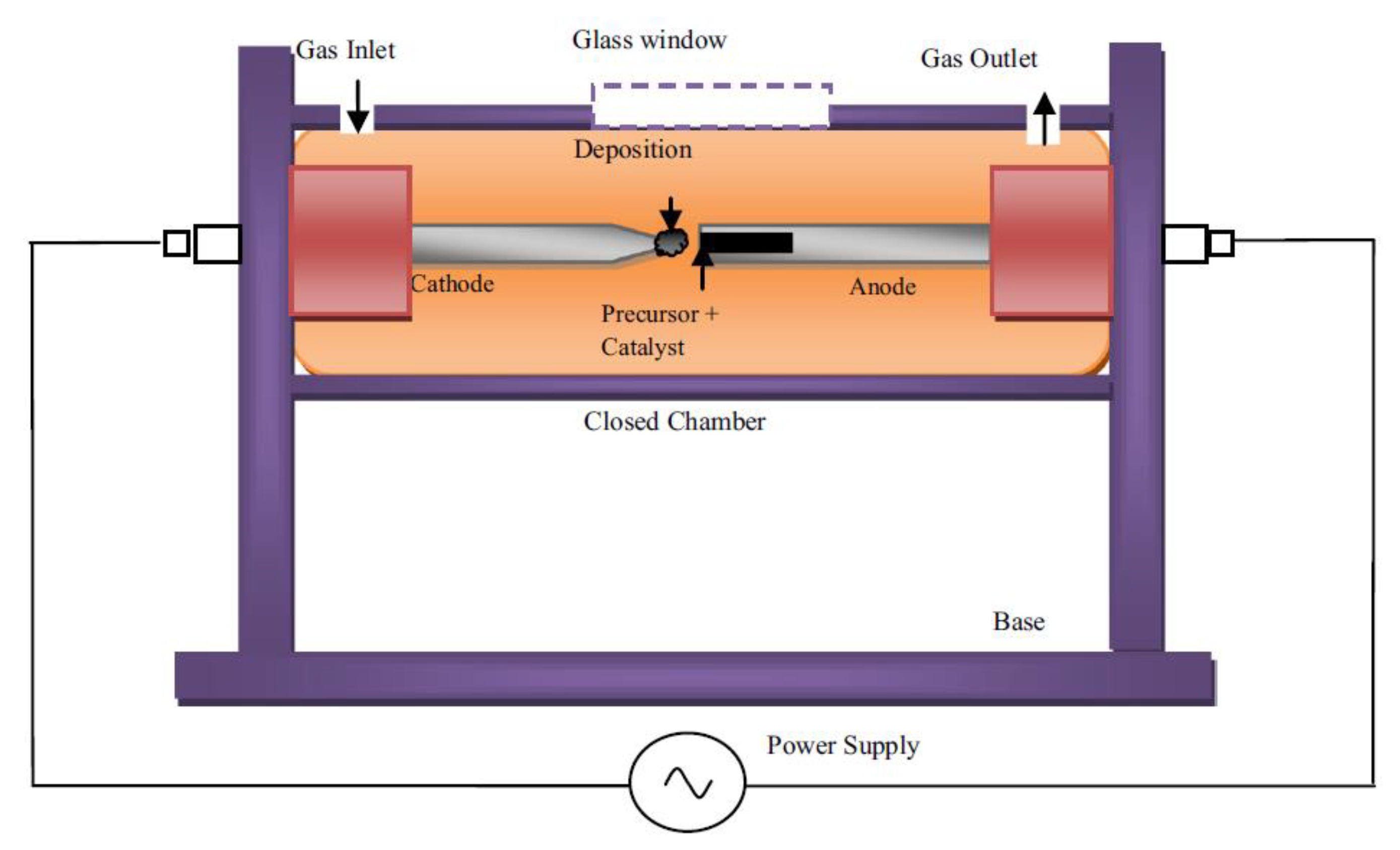
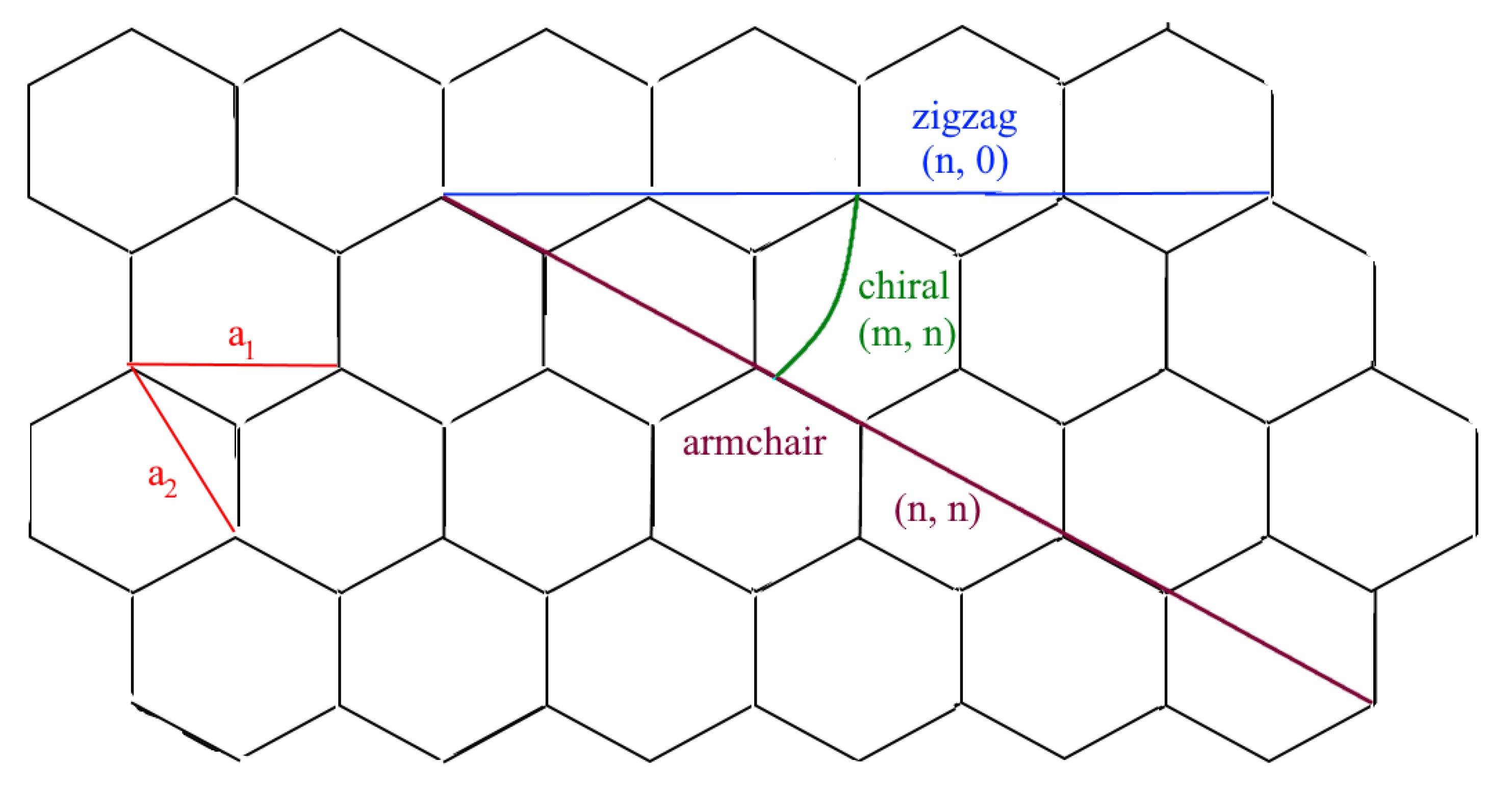
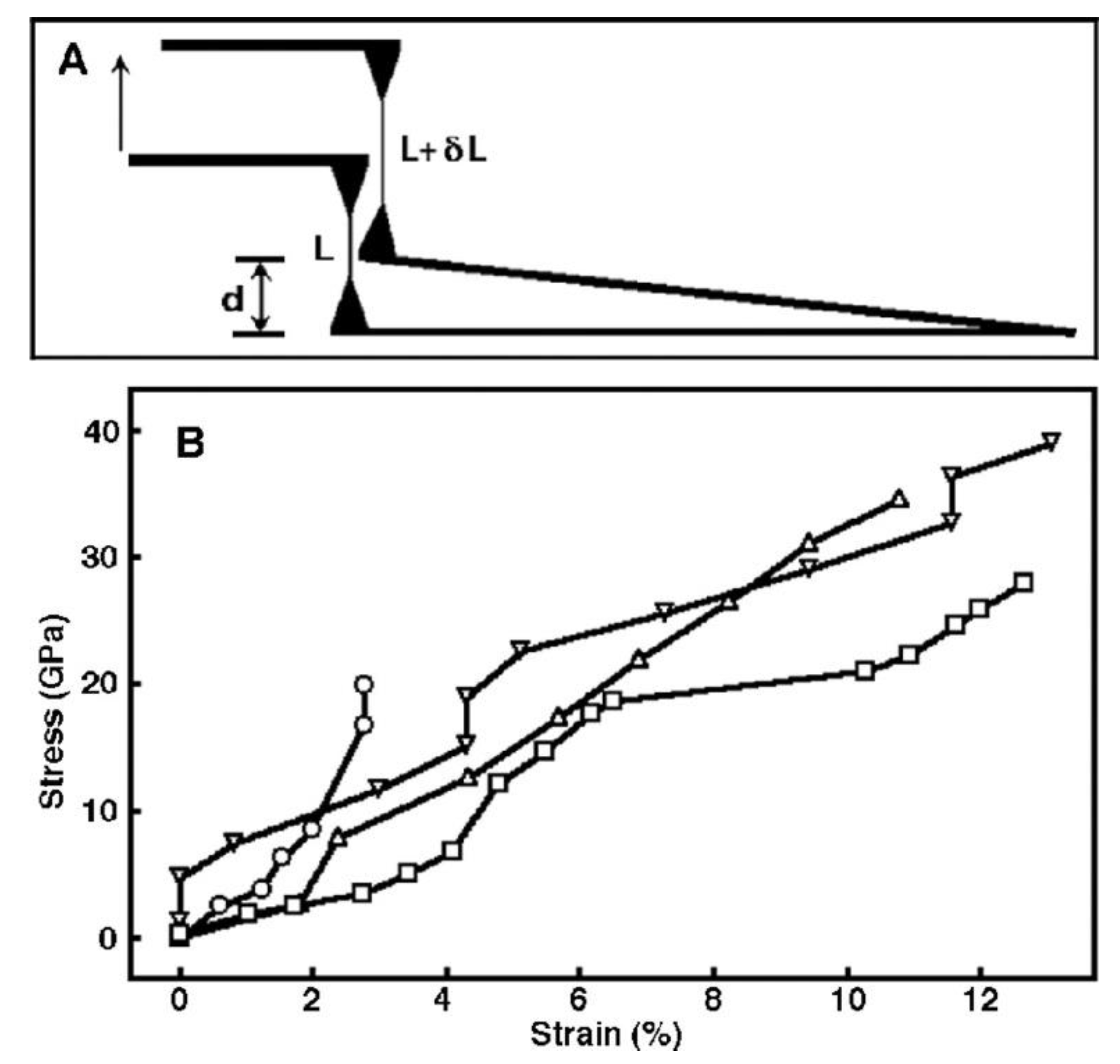
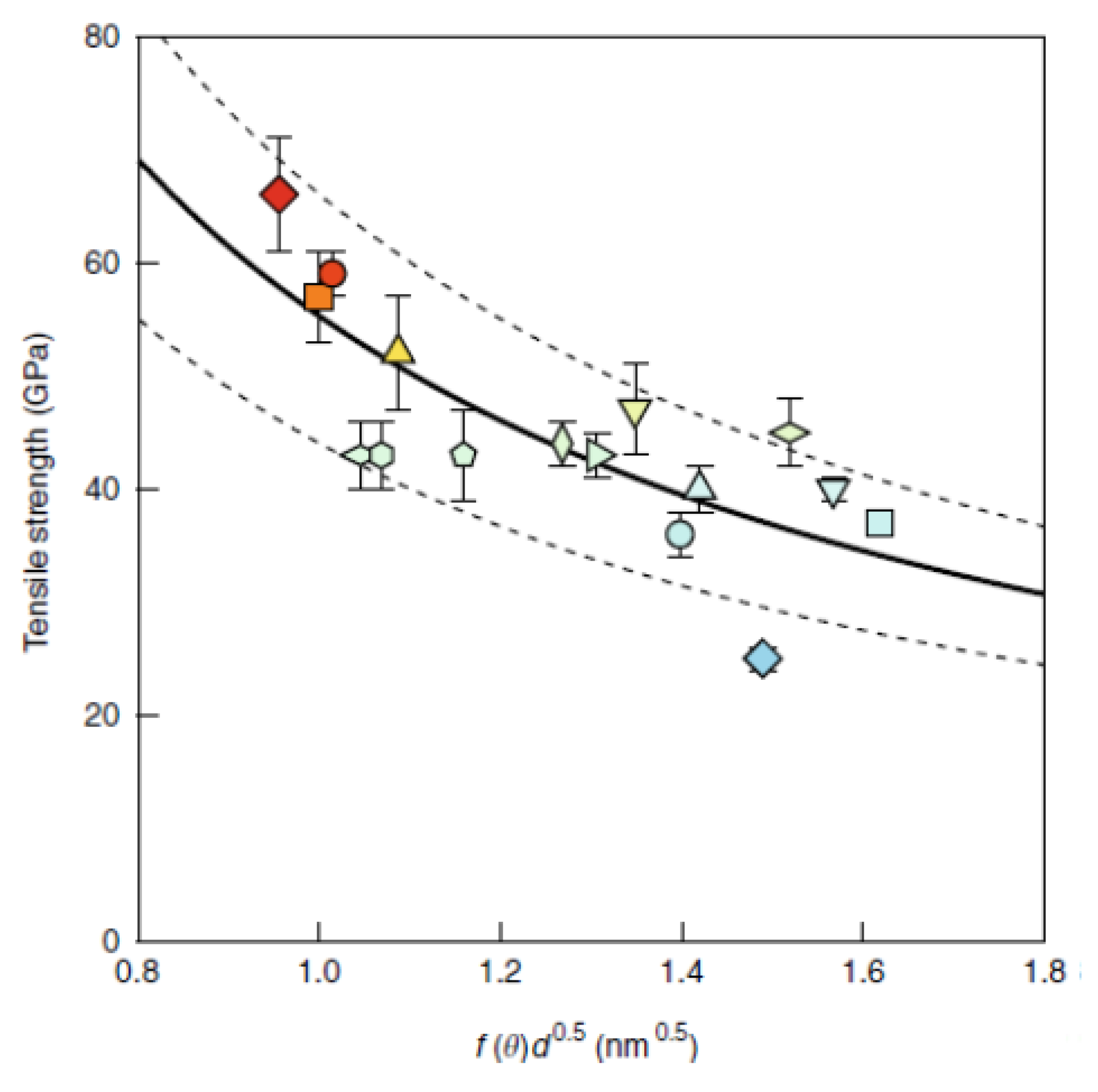
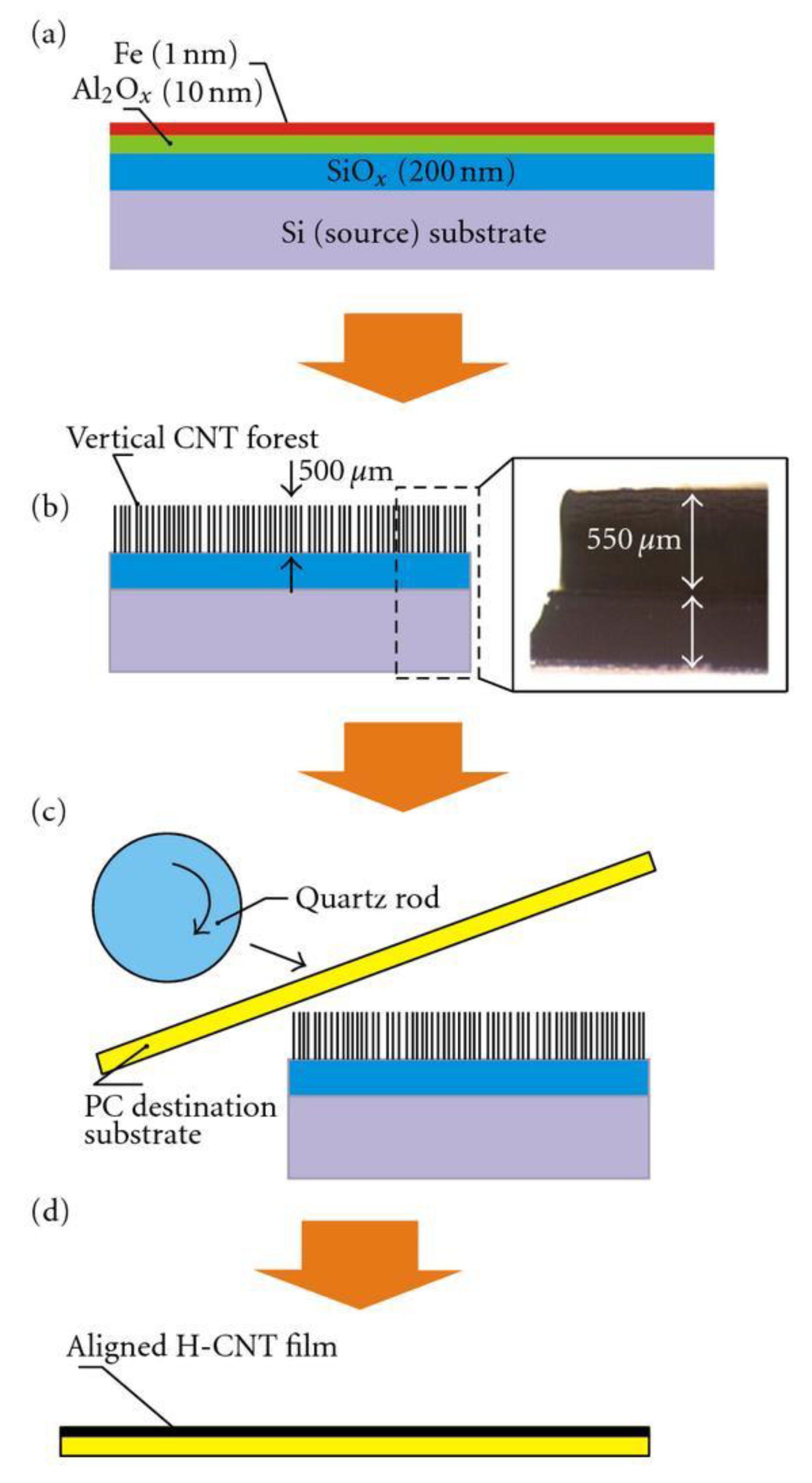
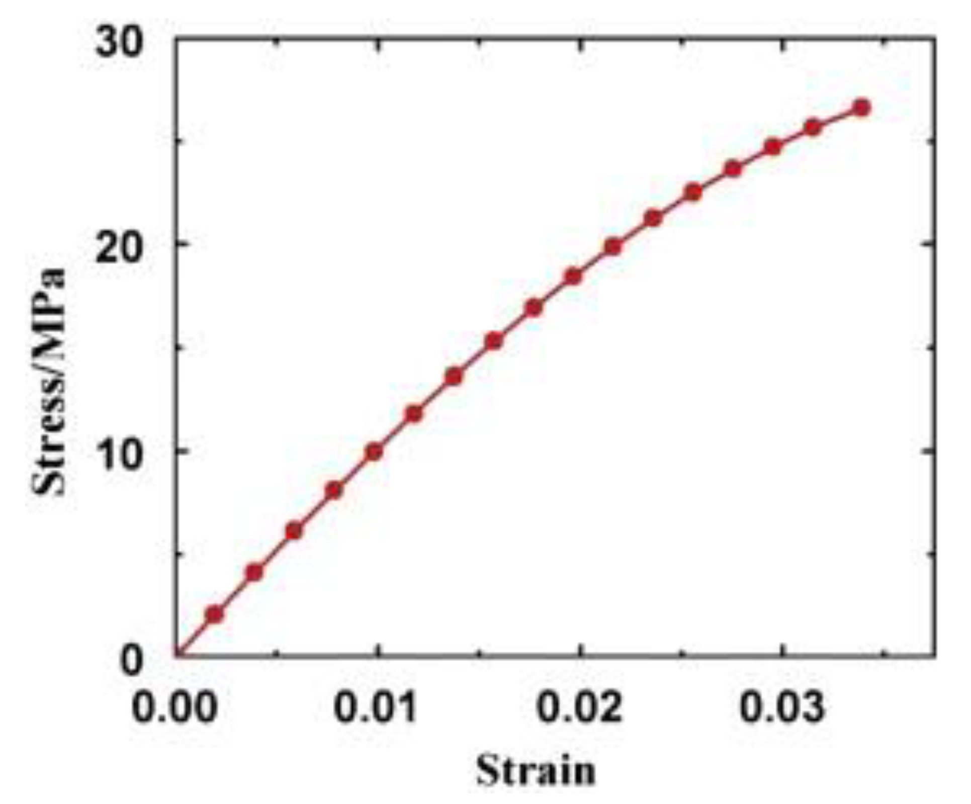
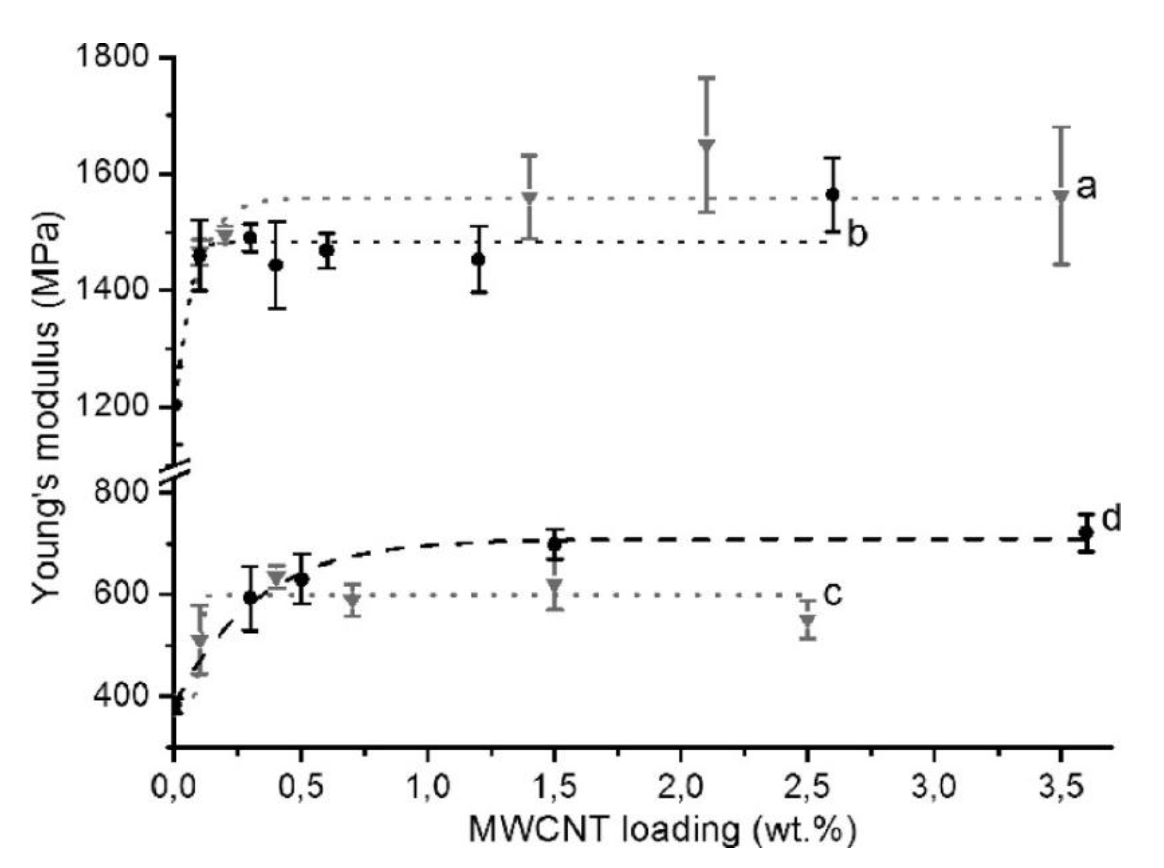
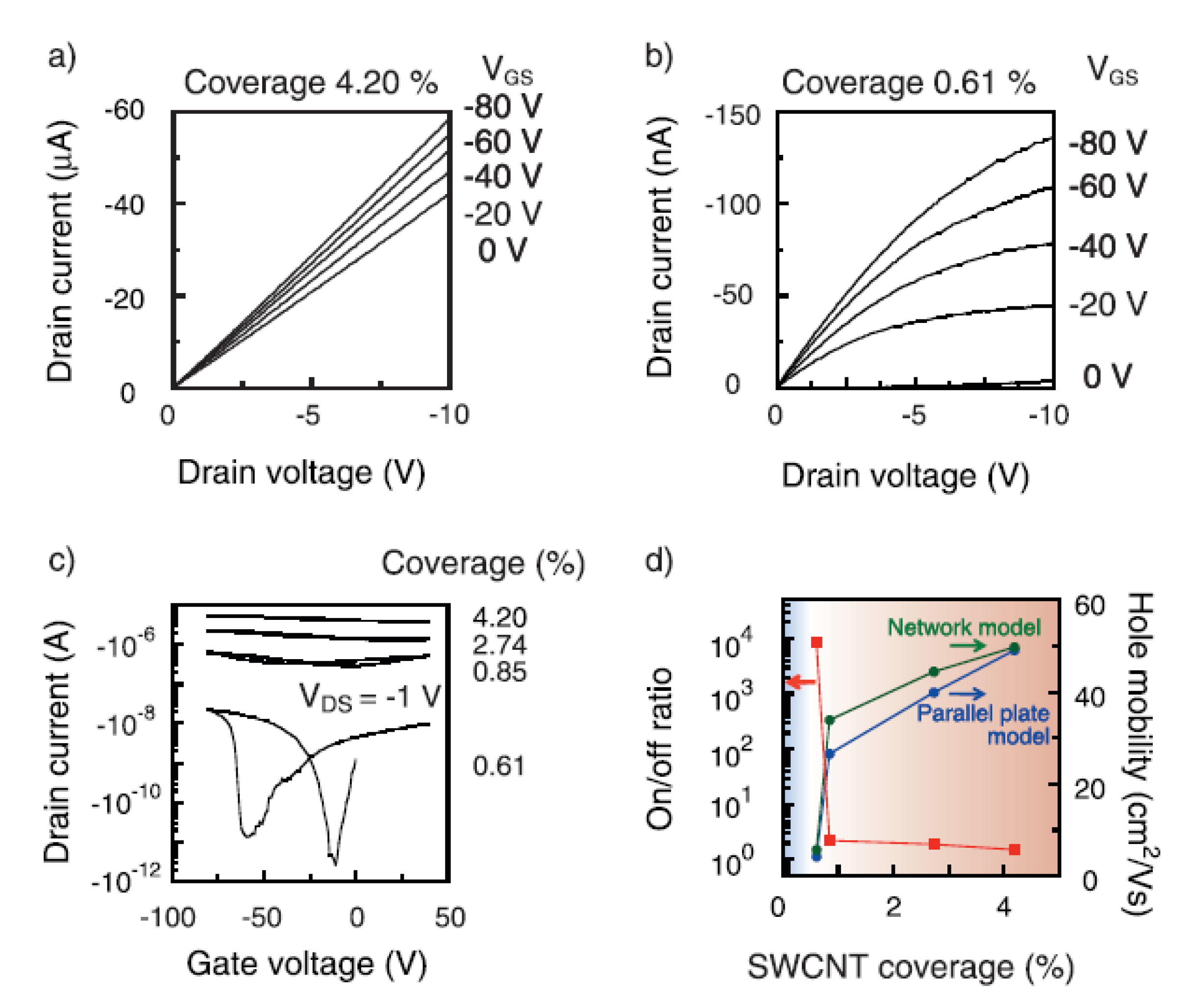
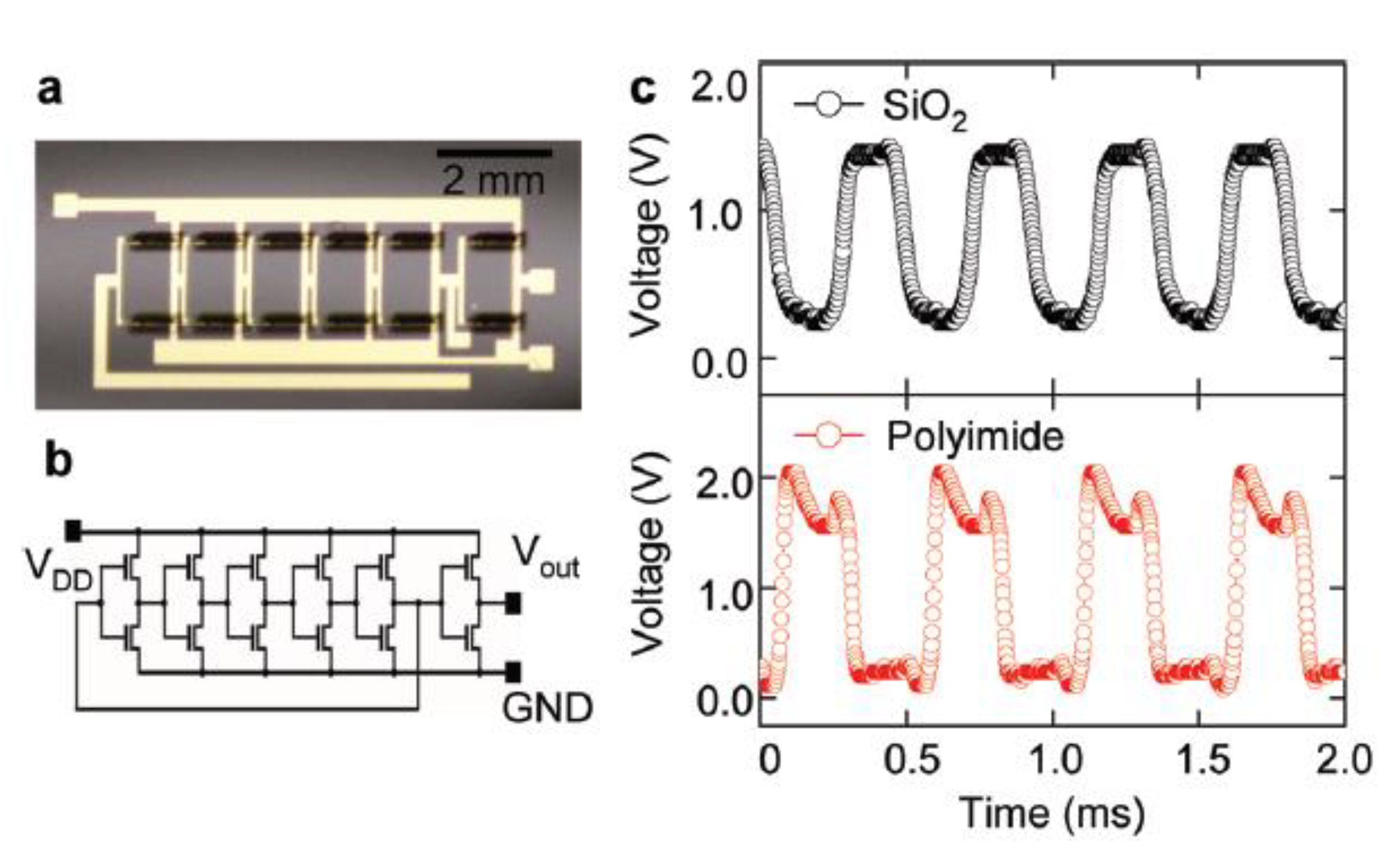
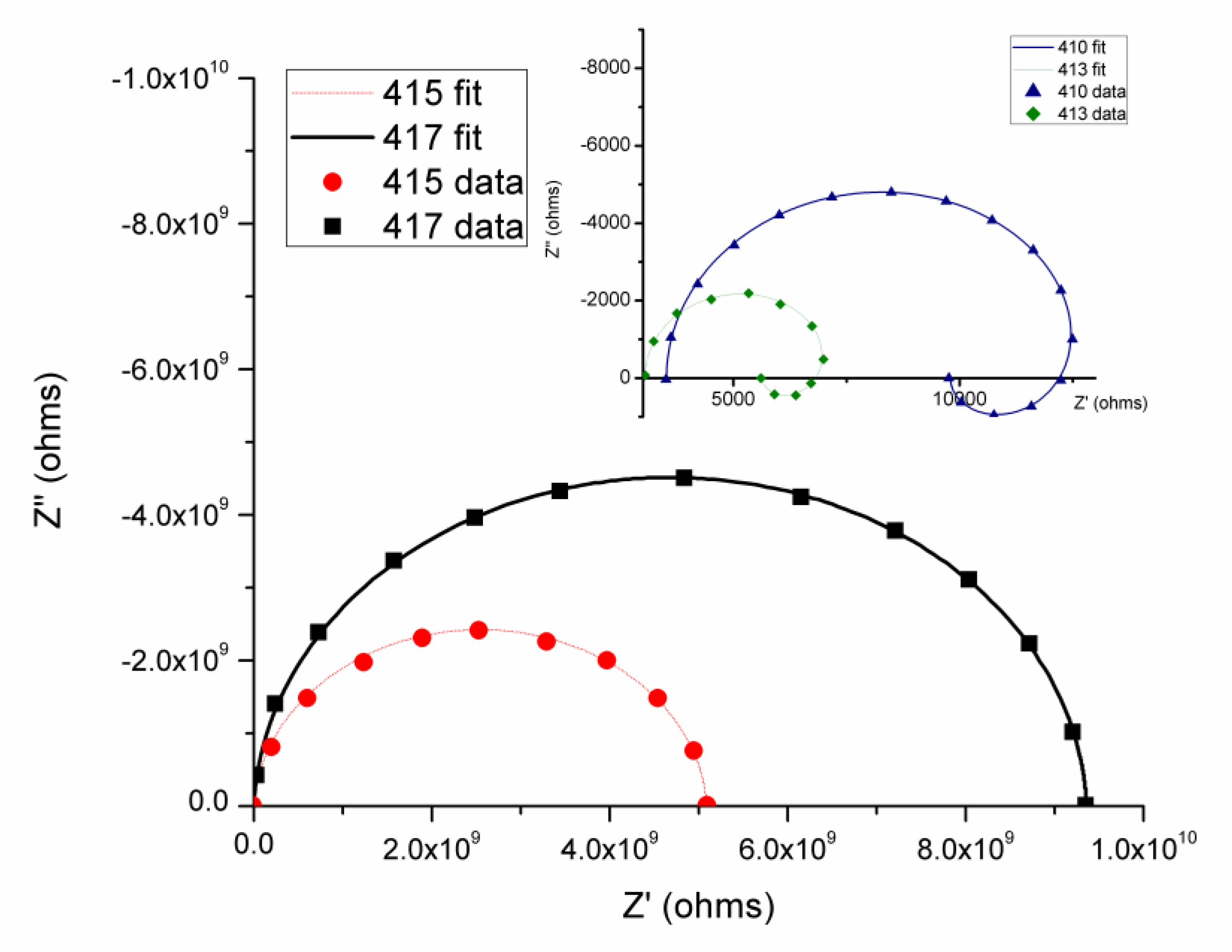
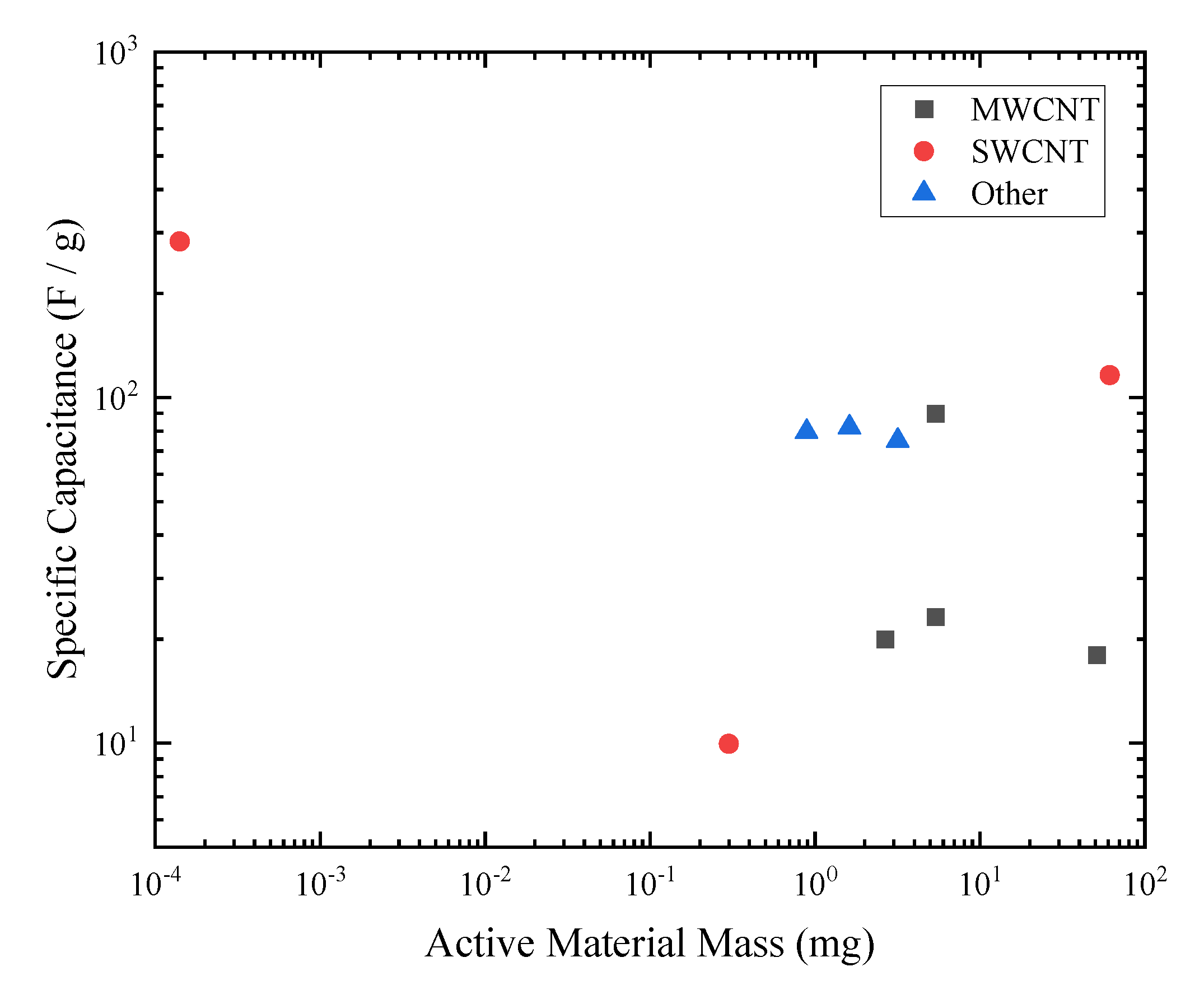
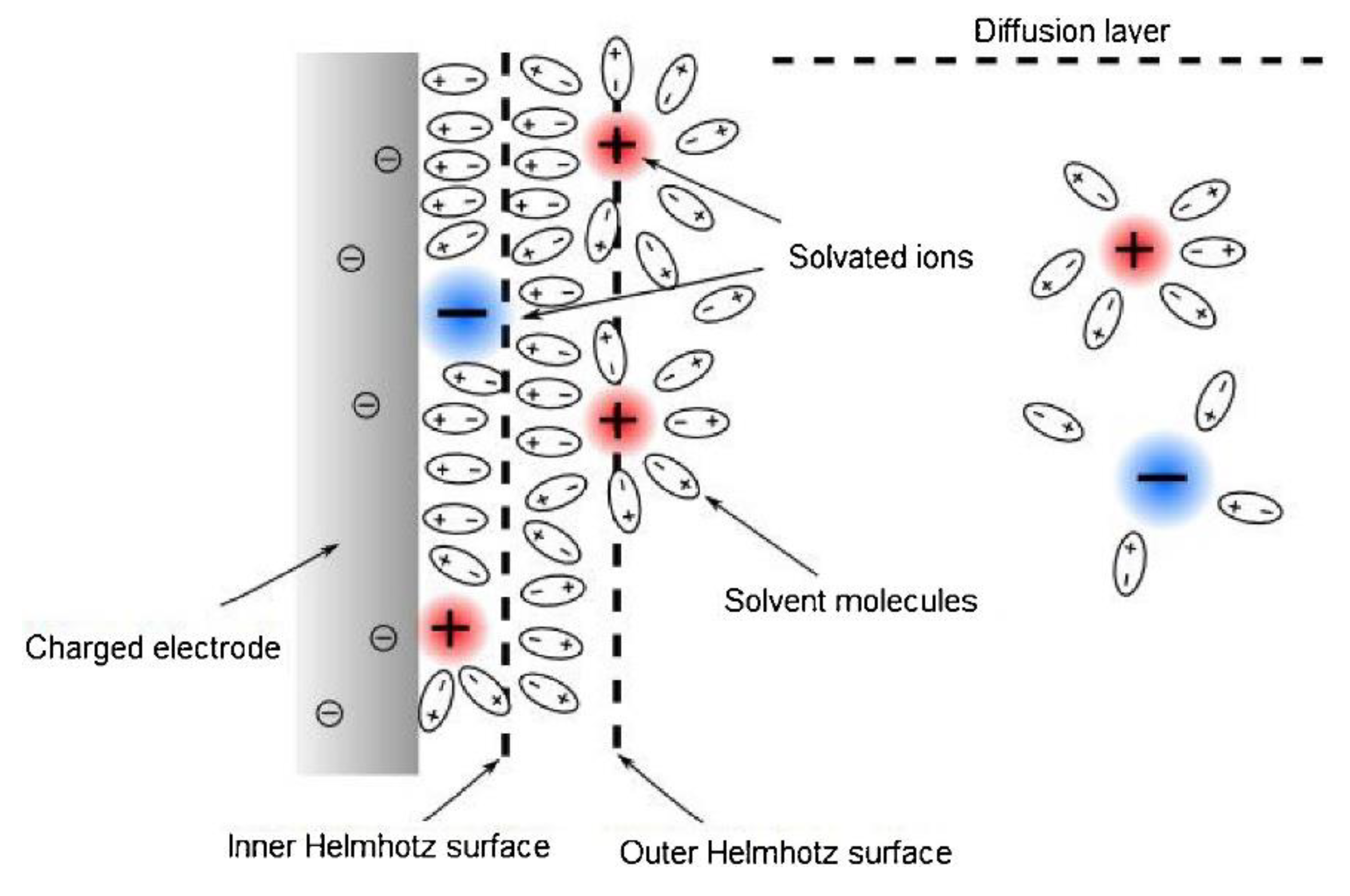
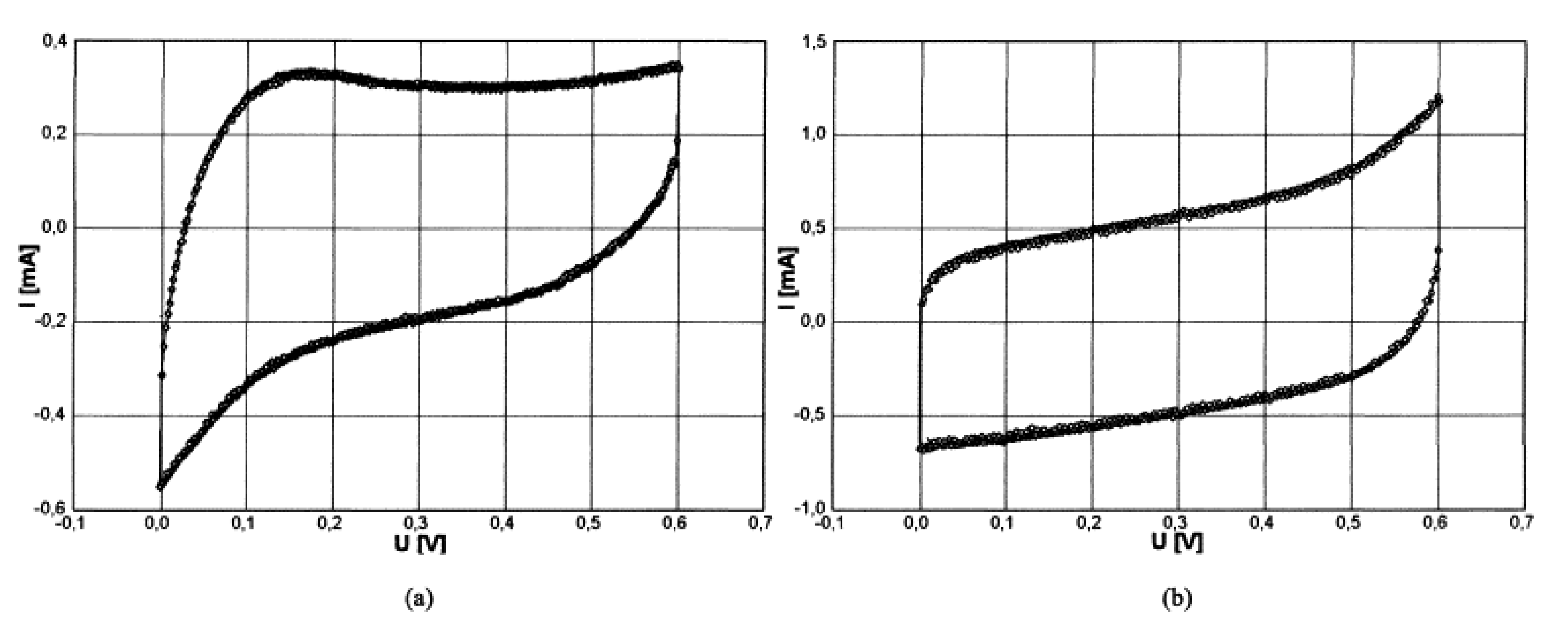
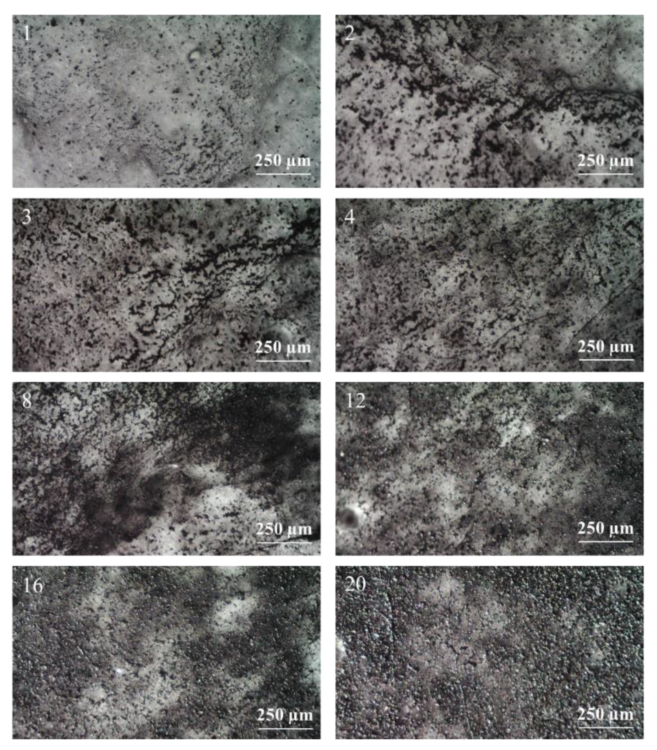
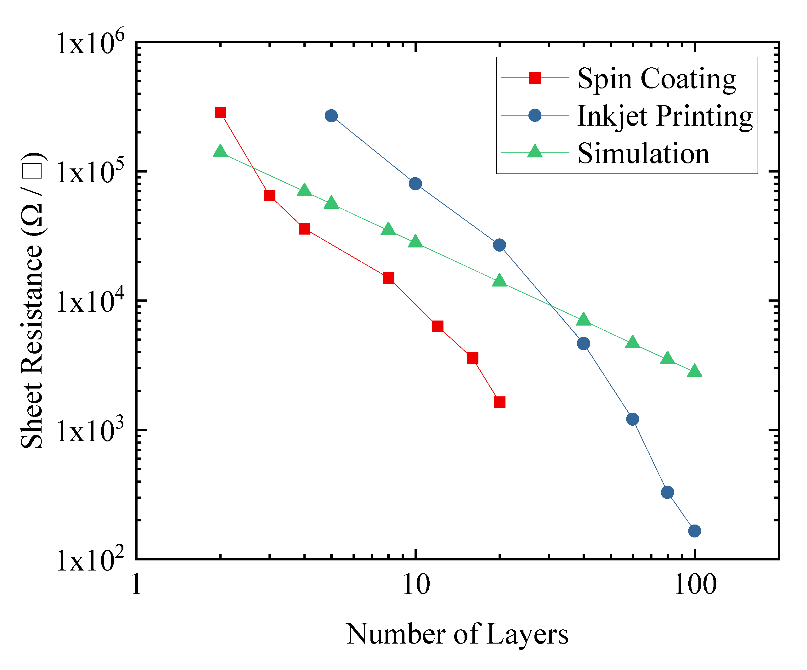
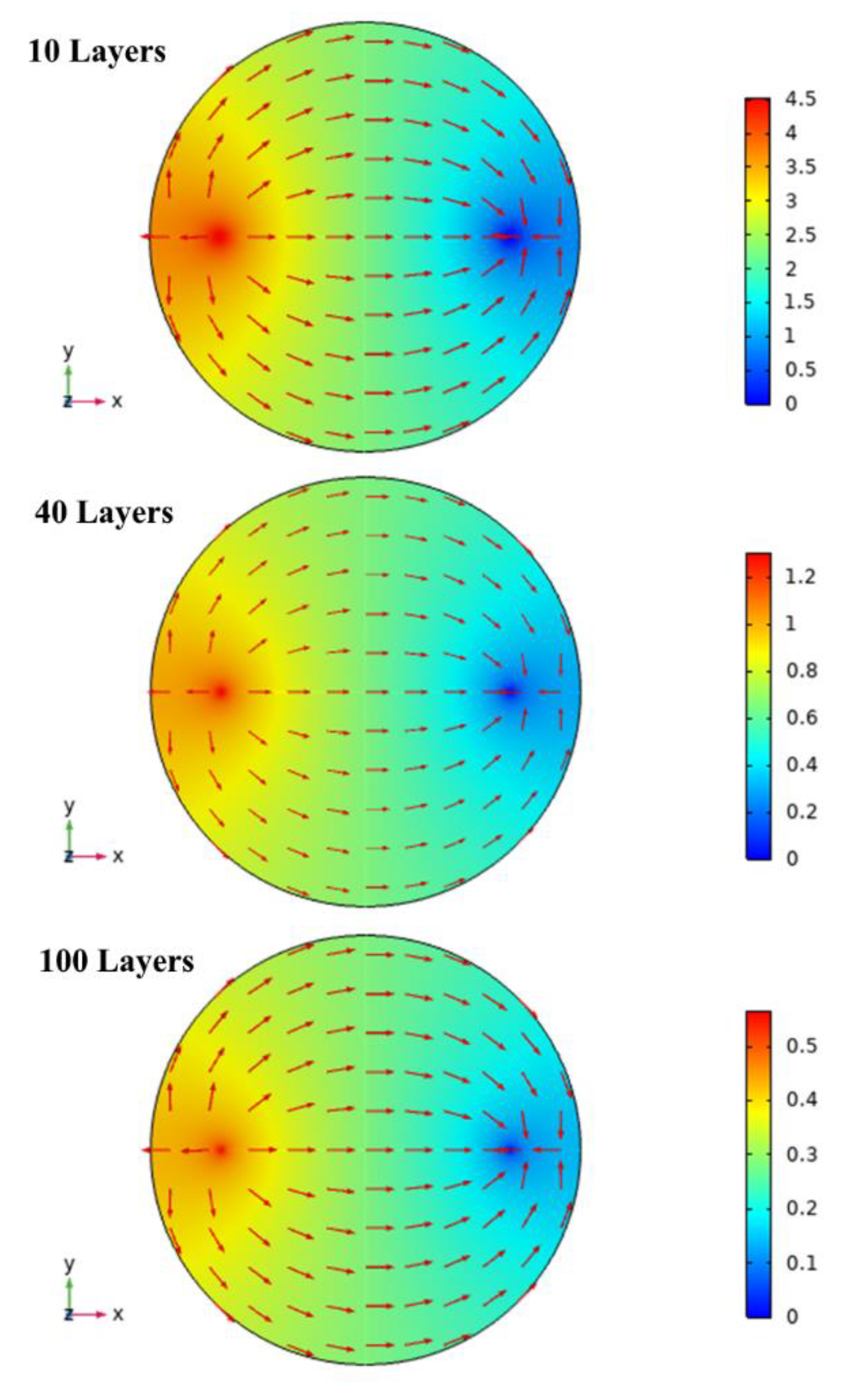
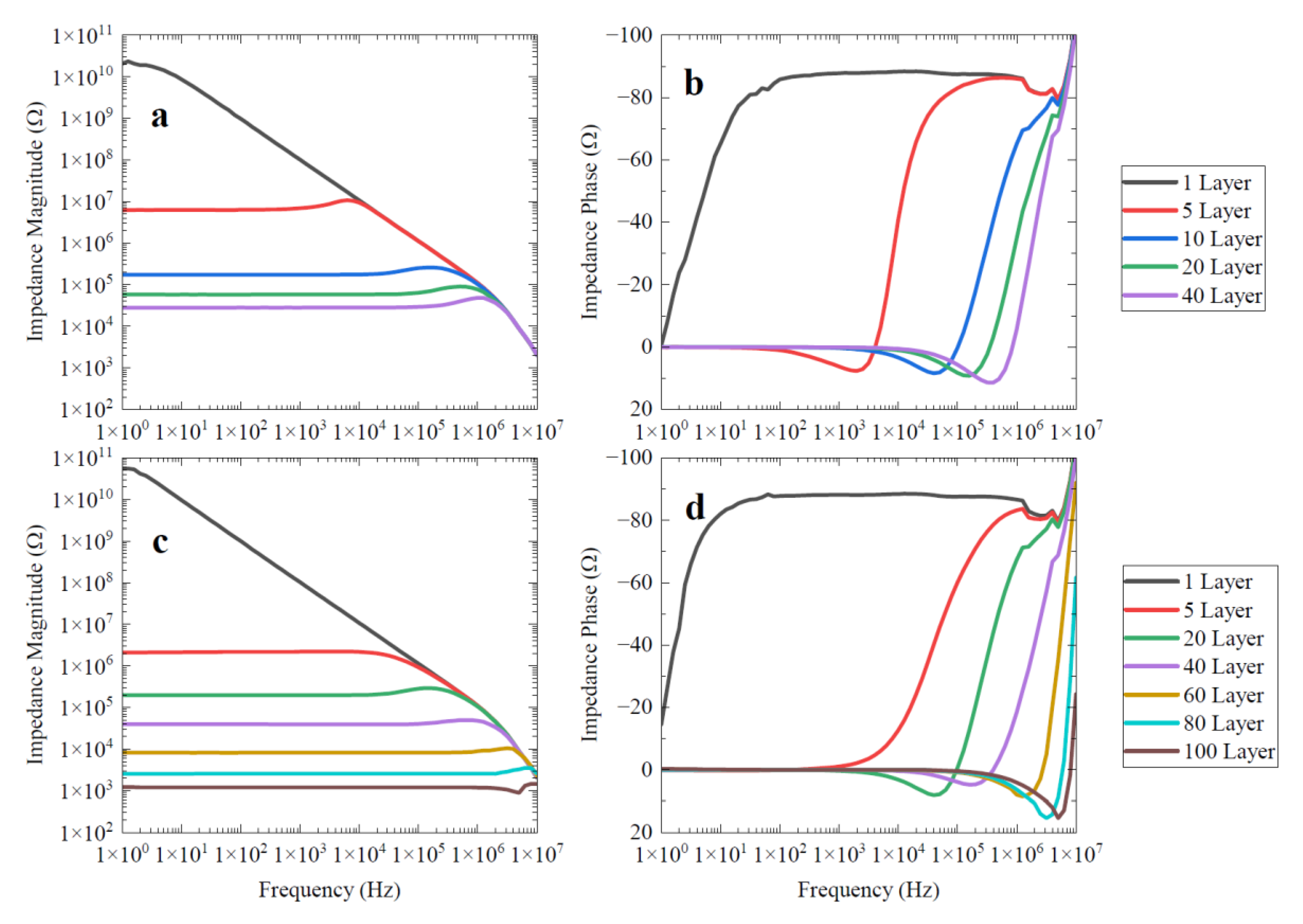
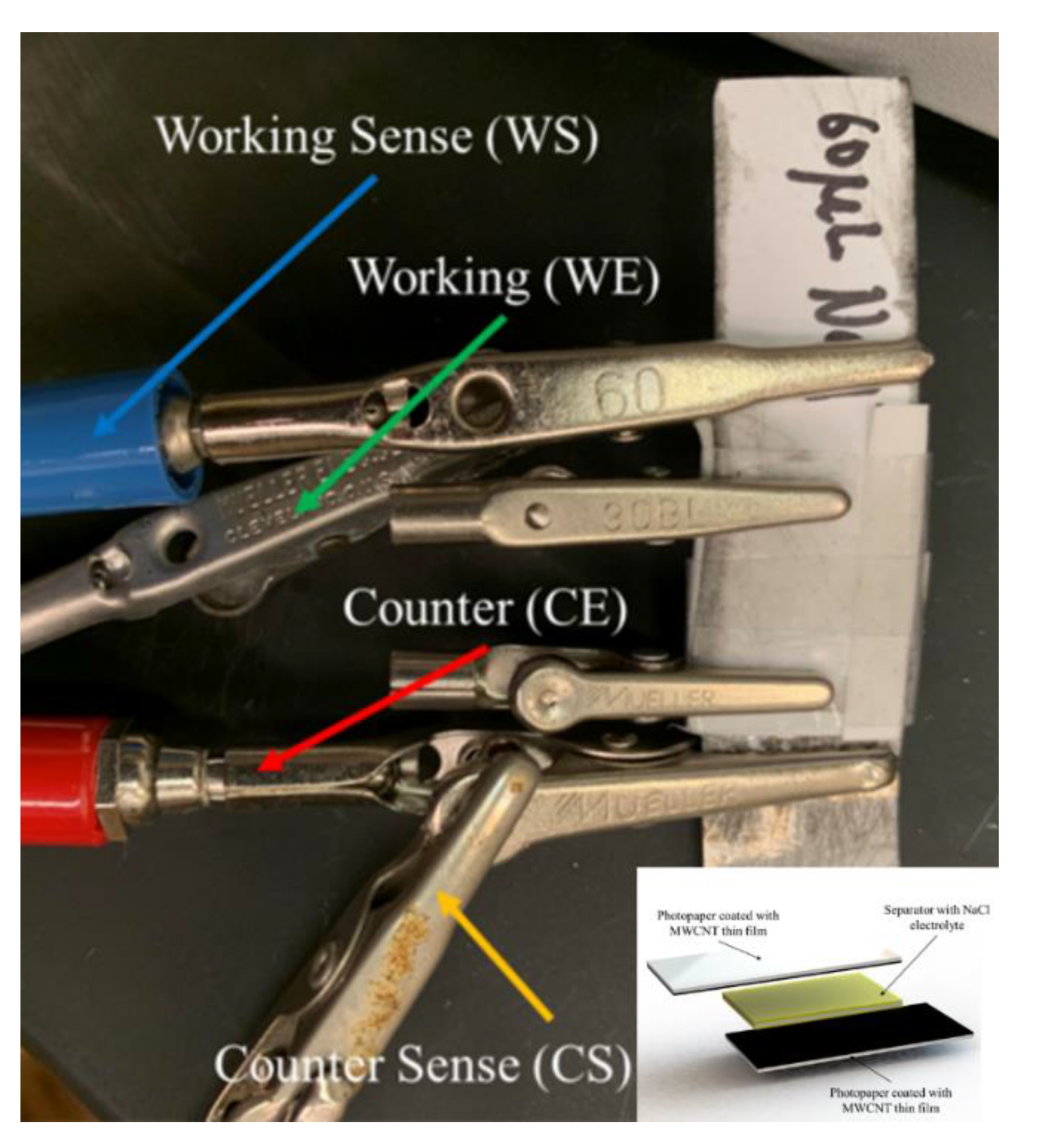
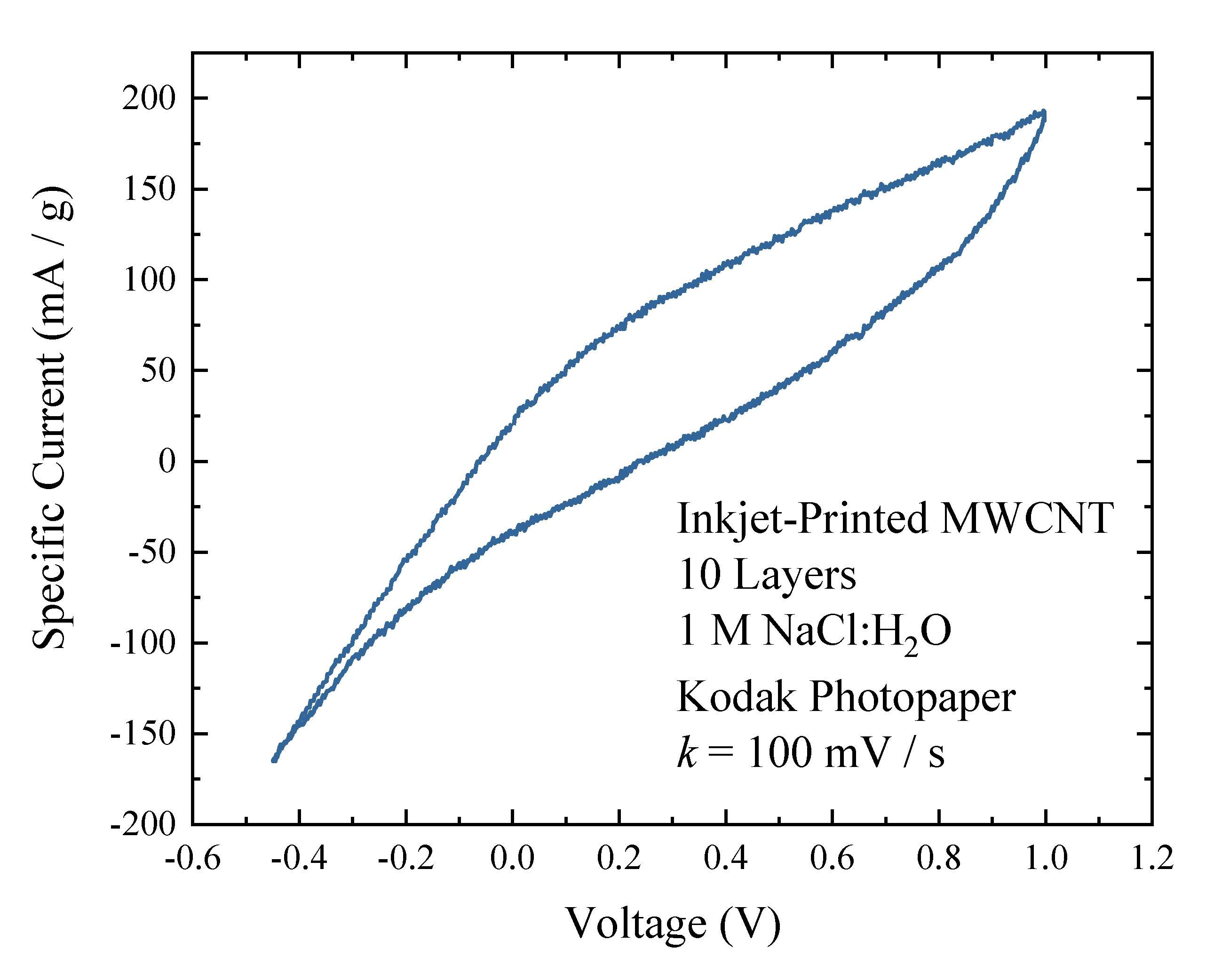
Table 1.
Schematics and applications of thin-film fabrication techniques for MWCNT dispersions and slurries.
Table 1.
Schematics and applications of thin-film fabrication techniques for MWCNT dispersions and slurries.
| Fabrication Technique | Description | Schematic | Applications |
|---|---|---|---|
| Dip coating | Substrate extracted from dispersion Thin film formed by evaporation and gravitational draining |  | Chemical sensing [43,44] Corrosion resistance [45] Biomedical [46] Supercapacitors [47,48] |
| Drop casting/Drying | Dispersion droplet placed on substrate Droplet optionally moved across substrate Evaporation removes solvent |  | Chemical sensing [49] Supercapacitors [50,51] Electrically conductive films [52] Gas separation [53] Photovoltaics [54] |
| Spin coating | Dispersion dropped onto rotating substrate Shearing force from rotation spreads dispersion over surface Evaporation removes solvent |  | Transparent films Photovoltaics [55,56] Electromagnetic shielding [57] |
| Inkjet printing | Electrical potential applied across piezoelectric nozzle, ejecting droplets on substrate Evaporation removes solvent |  | Electrically conductive films [58,59,60,61] Transistor devices [62,63,64,65] |
| Screen printing | Ink squeezed through open areas of a screen Ink is deposited on substrate Evaporation removes solvent |  | Piezoresistive pressure sensors [66,67,68] Bio sensing [69,70] Chemical sensing [43] Photovoltaics [55] |
| Meyer rod coating | Slurry is cast behind threaded rod Rod is translated without rotation over substrate |  | Supercapacitors [71,72] |
| Doctor blading | Slurry is cast in front of blade or in a reservoir Doctor blade is drawn over substrate Thickness of film is related to distance between blade and carrier |  | Supercapacitors |
Table 2.
Summary of previous investigations of carbon material-based electric double-layer supercapacitors.
Table 2.
Summary of previous investigations of carbon material-based electric double-layer supercapacitors.
| Active Material | Additives | Deposition Process | Active Material Details | Substrate Material/Surface Treatments | Post-Proessing | Electrolyte | Specific Capacitance [F/g] | Ref. |
|---|---|---|---|---|---|---|---|---|
| MWCNT | SDBS (surf.) | Spin coating/Inkjet printing | Spin coating: 400 μg (25 μg/layer, 8 layers) Inkjet printing: 60 μg (6.0 μg/layer, 10 layers) | Photo paper/UV ozone | N/A | 1 M NaCl in H2O | 0.02 | Current Work |
| MWCNT (acet. decomp.) | PVDF (bind.); acetylene black (cond.) | Pressing | 3.4–8.5 mg (85 wt% MWCNT, 4–10 mg total electrode mass) | Stainless steel | N/A | 6 M KOH | 4–135 | [93] |
| MWCNT (CCVD) | PTFE (bind.); carbon black (cond.) | Lamination | 51 mg (85 wt% active material, 15 mg/cm2, 4 cm2) | Aluminum/polyurethane paint (cond.) | N/A | 1.5 M NEt4BF4 in acetonitrile | 18 | [71] |
| MWCNT | PVDF (bind.); acetylene black (cond.) Activation with KOH | Pressing | 1.7–17 mg (85 wt% active material, 2–20 mg total) | Gold | N/A | 1 M H2SO4 | 90 | [94] |
| MWCNT | Mg(NO3)2 (EPD electrolyte) | Electrophoretic deposition | 0.8 cm × 0.8 cm (electrode area) | Nickel foil | Ar/H2 gas treatment | 6 N KOH | 21 | [135] |
| MWCNT | N/A | Colloid deposition and evaporation | 2.67 mg (26.7 mg/mL, 0.1 mL) | Nickel foil | Drying at room temperature | 6 M KOH | 20 | [50] |
| MWCNT | Nitric acid treatment | Drying | 25 μm (thickness), 800 mg/mL (MWCNT density) | N/A | Drying; thermally cross-linking | 38 wt% H2SO4 | 102 | [51] |
| MWCNT | Phenolic resin (PF) (bind.), nitric acid treatment | Molding | 1 g/cm3 (bulk density) | Graphite | Carbonization; Immersion in sulfuric/nitric acid | 38 wt% H2SO4 | 15–25 | [109] |
| MWCNT (aligned) | PPy (polymerization on MWCNTs) | Direct growth via pyrolysis of toluene and ferrocene | 100 μm (aligned MWCNT length); 0.16 cm2 (electrode area) | Gold-coated Mylar | N/A | 0.5 M KCl | 2.55 [F/cm2] | [136] |
| MWCNT/PPy | PPy (polymerization on MWCNTs) | Direct growth with Ni catalyst | 8–10 μm (aligned MWCNT length) | Titanium | Soaking in distilled water; bubbling in nitrogen (eliminate oxygen) | 0.1 M LiClO4 | N/A | [137] |
| MWCNT (in-plane aligned)/PPy | PPy (polymerization on MWCNTs) | MWCNT solution as polymerization | 0.2–2.5 μm (MWCNT length); 60 wt% MWCNTs | Graphite | N/A | 0.5 M KCl | 192 | [138] |
| SWCNT | Sulfuric acid/nitric acid treatment | Dip coating | 61.2 mg (by weighing) | Non-woven cotton paper | Drying at room temperature | PVA/phosphoric acid (solid) | 116 | [95] |
| SWCNT | SDBS (surf.) | Inkjet printing | 300 μg (0.3 mg/cm2, 1 cm2) | Newspaper; Kodak photo paper/PVDF coating | N/A | 1 M LiPF6 in EC: DEC | 3–33 | [96] |
| SWCNT | PVDC (bind.); THF (solv.) | Pressing | 150 μm (thickness of pellet), 750 mg/mL (SWCNT density) | Nickel foil/foam; Polishing | N/A | 38 wt% H2SO4 | 180 | [96] |
| SWCNT | SDS (surf.) | Suspension deposition and evaporation | 141 ng (by QCM) | Platinum | Heating in oven | 0.1 M TBAPF6 | 283 | [97] |
| SWCNT | N/A | Dip coating | 0.85 mg/cm2 | NTP | N/A | 3 M NaCl | 37.3 | [139] |
| SWCNT/PPy | PPy(polymerization on SWCNTs), PTFE (bind.), super P (cond.) | Pressing | 250 μm (electrode thickness) | Nickel foam | Vacuum drying | 7.5 M KOH | 265 | [140] |
| Activated Carbon (AC)/MWNT | PVDA or PVA (bind.) | Film application | 120 μm (thickness of AC/MWNT) | Aluminum foil | N/A | 1 M TEABF4 | 120 | [72] |
| Nanostructured Carbon | N/A | Cluster beam deposition | 3.17 mg (1 g/cm3 density, 6 cm × 6 cm × 0.8 μm) | Aluminum | N/A | Quartenary ammonium salt in PC | 75 | [98] |
| Graphene | N/A | Inkjet printing | 890 μg (8.9 μg/layer, 100 layers) | Titanium foil | Reduction of GO in flowing N2 | 1 M H2SO4 | 48–132 | [99] |
| Graphene/MWNT | Functionalized with nitric/sulfuric acid | Spray coating of MWCNTs onto CVD-grown graphene | 500 nm (thickness of MWNT film) | Polyethylene terephthalate (PET) | N/A | PVA-H3PO4 (gel) | 2.54 [mF/cm2] | [110] |
| Graphene/MWNT foam | Activation with KOH | Foam grown via one-step ambient pressure CVD | Nickel foam | Cooling to room temperature | 6 M KOH | 286 | [141] | |
| Graphene/PANI | SDBS (surf.) | Inkjet printing | 1.62 mg (800 × 800 array, 13 μm separation, 1.5 mg/cm2) 5 layers | Quartz; carbon fabric | N/A | 1 M H2SO4 | 82 | [100] |
Publisher’s Note: MDPI stays neutral with regard to jurisdictional claims in published maps and institutional affiliations. |
© 2021 by the authors. Licensee MDPI, Basel, Switzerland. This article is an open access article distributed under the terms and conditions of the Creative Commons Attribution (CC BY) license (https://creativecommons.org/licenses/by/4.0/).
Share and Cite
MDPI and ACS Style
Jiang, K.; Gerhardt, R.A. Fabrication and Supercapacitor Applications of Multiwall Carbon Nanotube Thin Films. C 2021, 7, 70. https://0-doi-org.brum.beds.ac.uk/10.3390/c7040070
AMA Style
Jiang K, Gerhardt RA. Fabrication and Supercapacitor Applications of Multiwall Carbon Nanotube Thin Films. C. 2021; 7(4):70. https://0-doi-org.brum.beds.ac.uk/10.3390/c7040070
Chicago/Turabian StyleJiang, Kyle, and Rosario A. Gerhardt. 2021. "Fabrication and Supercapacitor Applications of Multiwall Carbon Nanotube Thin Films" C 7, no. 4: 70. https://0-doi-org.brum.beds.ac.uk/10.3390/c7040070
Note that from the first issue of 2016, this journal uses article numbers instead of page numbers. See further details here.