
Temperature Sensors Based on Organic Field-Effect Transistors


Department of Chemical Engineering, Waterloo Institute for Nanotechnology (WIN), University of Waterloo, Waterloo, ON N2L 3G1, Canada
*
Author to whom correspondence should be addressed.
Chemosensors 2022, 10(1), 12; https://0-doi-org.brum.beds.ac.uk/10.3390/chemosensors10010012
Submission received: 5 December 2021
/
Revised: 22 December 2021
/
Accepted: 22 December 2021
/
Published: 27 December 2021
(This article belongs to the Special Issue Functionalized Organic Thin Film Transistors for Sensing)
Abstract
:The rapid growth of wearable electronics, Internet of Things, smart packaging, and advanced healthcare technologies demand a large number of flexible, thin, lightweight, and ultralow-cost sensors. The accurate and precise determination of temperature in a narrow range (~0–50 °C) around ambient temperatures and near-body temperatures is critical for most of these applications. Temperature sensors based on organic field-effect transistors (OFETs) have the advantages of low manufacturing cost, excellent mechanical flexibility, easy integration with other devices, low cross-sensitivity, and multi-stimuli detectability and, therefore, are very suitable for the above applications. This article provides a timely overview of research progress in the development of OFET-based temperature sensors. First, the working mechanism of OFETs, the fundamental theories of charge transport in organic semiconductors, and common types of OFET temperature sensors based on the sensing element are briefly introduced. Next, notable advances in the development of OFET temperature sensors using small-molecule and polymer semiconductors are discussed separately. Finally, the progress of OFET temperature sensors is summarized, and the challenges associated with OFET temperature sensors and the perspectives of research directions in this field are presented.

1. Introduction
Organic field-effect transistors (OFETs) or organic thin-film transistors (OTFTs) use organic semiconductors (OSCs) including covalent organic frameworks (COFs) and metal-organic frameworks (MOFs) as active channel materials, which enables the high-speed fabrication of electronic products on flexible plastic substrates under mild conditions at an ultralow cost [1,2,3,4,5,6]. OFETs have a wide range of applications, such as flexible displays, smart labels, intelligent packaging, various types of sensors, wearable electronics, implantable electronics, etc. OFET-based sensors, in particular, are ultralow in cost and can be integrated with other electronics as on-chip sensors, making them an excellent fit for the rapidly growing Internet of Things (IoT) technology, wearable electronics, and healthcare applications [7,8,9,10,11].
Temperature determination is one of the most common applications for modern-day sensors. The field of medicine has a demand for high functioning temperature sensors to be used in vital sign monitoring [12,13,14]. Furthermore, recent developments towards designing artificial skin, or electronic skin (e-skin), require accurate temperature monitoring as well as flexible systems with spatial resolution for practical application [15,16]. Temperature determination is also imperative for monitoring other physical parameters such as pressure, humidity, and gas concentration, which can have a temperature dependence and cannot be accurately determined without adjusting for temperature fluctuation [17].
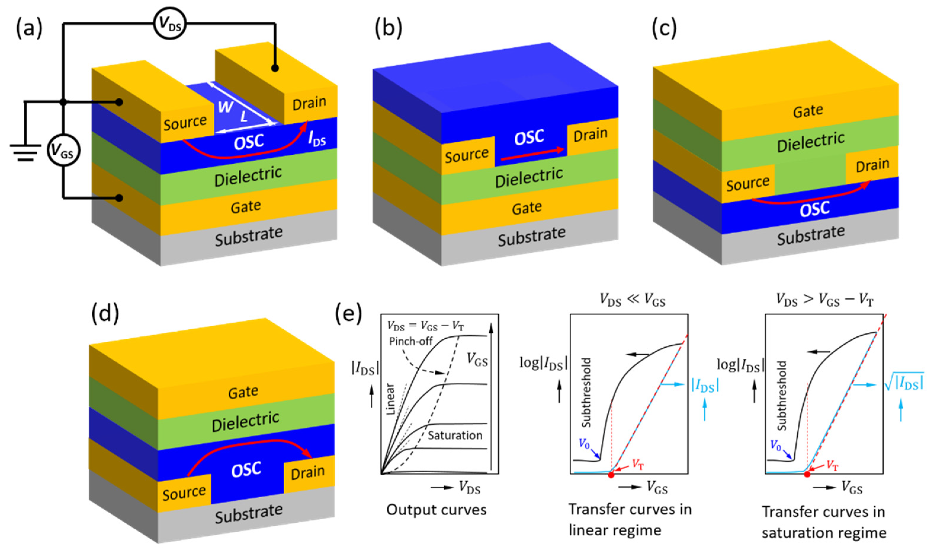
Similar to a conventional metal oxide semiconductor field-effect transistor (MOSFET), an OFET device consists of three electrodes (source, drain, and gate), a dielectric layer, and an organic semiconductor layer. Figure 1 shows the four common structures of OFETs, bottom-gate top-contact (BGTC), bottom-gate bottom-contact (BGBC), top-gate top-contact (TGTC), and top-gate bottom-contact (TGBC). The OFET current-voltage characteristics are schematically shown in Figure 1e. The output characteristics illustrate the changes of the drain current (IDS) with the drain voltage (VDS) at different gate voltages (VGS). At a very low VDS, the IDS-VDS relationship is ohmic (linear), and this region is called the linear regime (or region). As VDS increases, IDS increases at a slower rate, and the I-V curve becomes non-linear. After VDS reaches a certain point, where VDS = VGS − VT, IDS becomes independent of VDS, and the channel is called pinched off. VT here is the threshold voltage, which is the minimum gate voltage required to fill the charge traps at the channel. The region where VDS > VGS − VT is called the saturation regime. The changes of IDS with VGS at a fixed VDS are the transfer characteristics. In the linear regime (VDS << VGS), IDS and VGS have the following relationship [18,19]:
where W is the channel width, L is the channel length, μlin is the field effect mobility in the linear regime, and Ci is the capacitance of the dielectric layer.
From the IDS-VGS curve, μlin can be extracted:
In the saturation regime (VDS > VGS − VT), IDS and VGS have the following relationship:
where IDS,sat and μsat are the drain current and mobility in the saturation regime, respectively.
μsat can be calculated from the saturation transfer curves using the following equation:
Similar to the conventional resistor-type temperature sensor, or thermistor, the sensitivity of the OFET sensor can be described using the thermal coefficient of resistance (TCR), which can be calculated by
where R is the resistance of the channel at a given temperature, R0 is the resistance of the channel at a known reference temperature, and ΔT is the difference between the sensing and reference temperatures [20]. For OFET devices, the ratio of can be easily calculated using the variation of IDS with the temperature at constant VGS and VDS, .
The conventional two-electrode resistor-type temperature sensor can only give one independent output parameter, such as current or voltage. The change in current or voltage may be induced by interfering stimuli such as pressure and humidity, causing cross-sensitivity issues. On the other hand, the OFET temperature sensor can provide numerous parameters, such as IDS and VDS (in different regimes), onset voltage (V0), threshold voltage (VT), and mobility (μ) [18,19]. This multi-parameter sensing capability enables OFET temperature sensors to distinguish temperature-induced parameter changes from pressure, light, chemical substances, and other stimuli-induced changes, providing high selectivity and reliability of multi-functional sensing [21,22].
Organic materials are composed of molecules as the basic building blocks, which are made of carbon, oxygen, hydrogen, nitrogen, and other elements. The constituent atoms in an organic molecule are strongly held with covalent bonds between atoms by sharing the valence electrons. Therefore, most organic materials are insulators because valence electrons are highly localized. A characteristic of organic semiconductors is that their skeleton has an extended π-conjugated system, usually composed of alternating C–C and C=C bonds. The overlapping (or hybridization) of the molecular orbitals forms an extended highest occupied molecular orbital (HOMO) and a lowest unoccupied molecular orbital (LUMO), where the injected holes (in HOMO) and electrons (in LUMO) can move relatively easily. As the molecular size increases, such as in the case of high molecular weight polymers, long-range π conjugation results in a band-like structure with a small band gap (<3 eV) between HOMO and LUMO, similar to typical inorganic semiconductors. However, organic molecules are held together by weak van der Waals forces or London dispersion forces to form a solid, so the intermolecular distance is quite large, usually 0.3–0.4 nm. This makes intermolecular charge transport more difficult than intramolecular charge transport. Organic molecules are much larger than the spherical constituent atoms and ions in inorganic materials and have more complex geometric shapes. Therefore, most organic semiconductors are disordered (polycrystalline or amorphous), which makes charge transport in organic semiconductors even more difficult and highly dependent on the processing conditions of the material. As a result, the charge transport mechanism in organic semiconductors is extremely complicated and has been a subject of extensive study since its discovery.
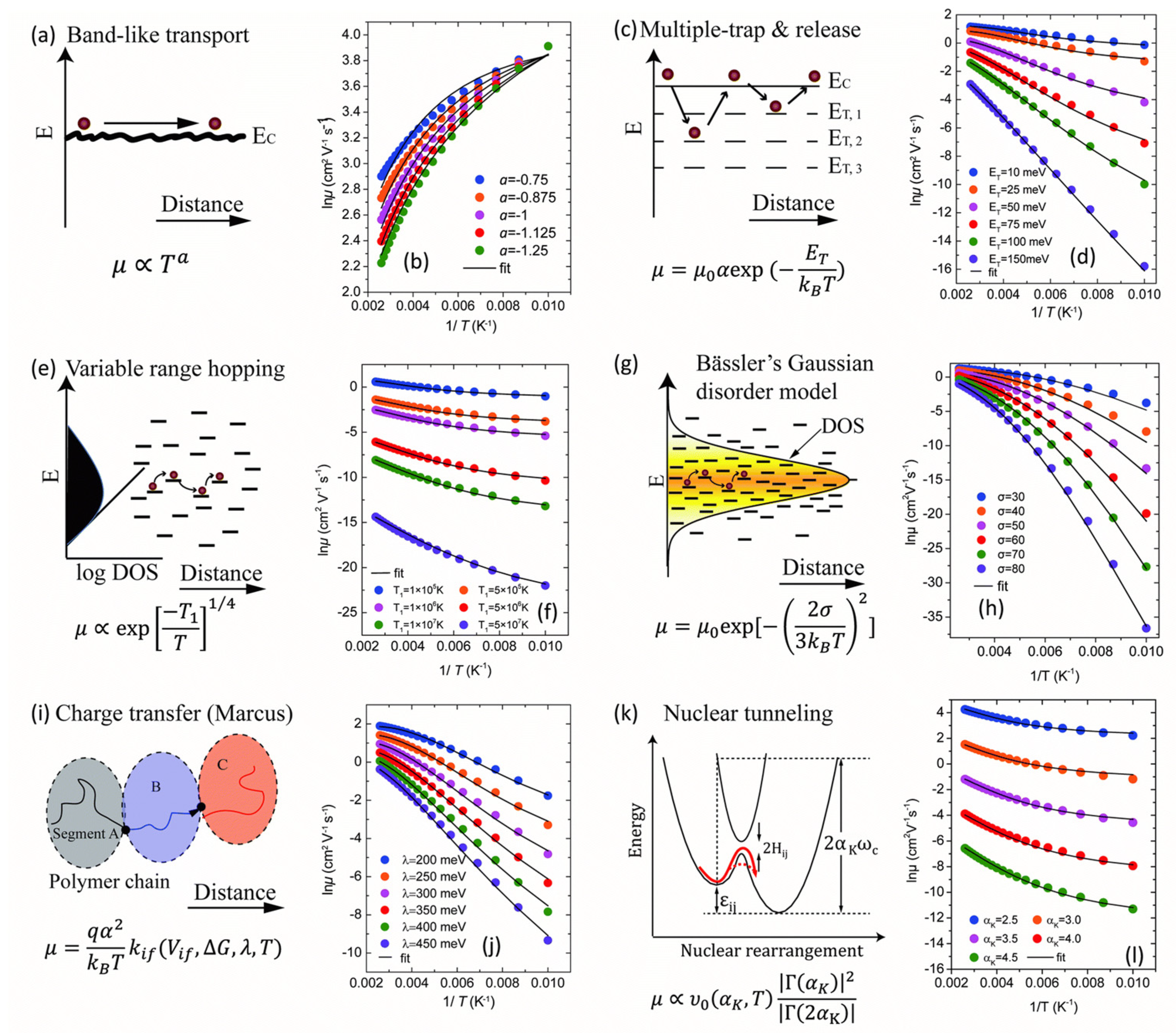
Numerous charge transport models have been proposed for organic semiconductors, including multiple trapping and release (MTR), variable range hopping (VRH), band-like transport, percolation model, and Gaussian disorder model (GDM), according to the type of material, degree of crystallinity, temperature range, applied voltage, etc. [23,24,25,26,27].
As shown in Figure 2, the charge carrier mobility of organic semiconductors may increase or decrease with increasing temperature, depending on the model, which results in a decrease in resistance (a negative temperature coefficient, NTC) or an increase in resistance (a positive temperature coefficient, PTC), respectively. Since IDS in the linear (Equation (1)) or saturated (Equation (2)) regime is a function of the carrier mobility of the organic semiconductor channel, it can be used as an output signal to detect the temperature change. MTR and VRH models, in which mobility increases with temperature, are most widely used in polycrystalline or amorphous organic semiconductors. Some highly crystalline small molecules [28,29,30,31] and polymers [32,33,34,35] have been found to follow a “band-like” transport model around room temperature, in which mobility decreases with temperature. The mobility of organic semiconductors is also field dependent [23,24], and the field-effect mobility is often strongly dependent on the gate voltage [27]. Consequently, the sensitivity of an OFET temperature sensor may also be influenced by the voltage applied.
Deep charge carrier traps in the organic semiconductor or the dielectric layer near their interface must be filled before a significant current flows in the channel; therefore, a larger number of deep traps leads to an increase in the threshold voltage (VT) and the onset voltage (V0) [18,19,37]. As temperature increases, some deep traps become shallow traps, resulting in a decrease in VT and V0 [36,37]. Therefore, VT or V0 can be directly used as a parameter to detect the temperature change. As shown in Equations (1) and (2) and Figure 1, IDS in the subthreshold region is also significantly dependent on the threshold voltage VT and hence on the temperature.
IDS is proportional to the capacitance (Ci) of the dielectric layer (Equations (1) and (2)), while Ci is proportional to the relative permittivity or dielectric constant (k) of the dielectric material: Ci = kC0, where C0 is the vacuum capacitance. The properties of the dielectric layer material, such as dielectric constant and surface trap density, also have a profound impact on IDS, VT, and even mobility [38]. Therefore, a dielectric material whose properties change dramatically with temperature can induce significant changes in OFET parameters and thus can be used as a sensor element.
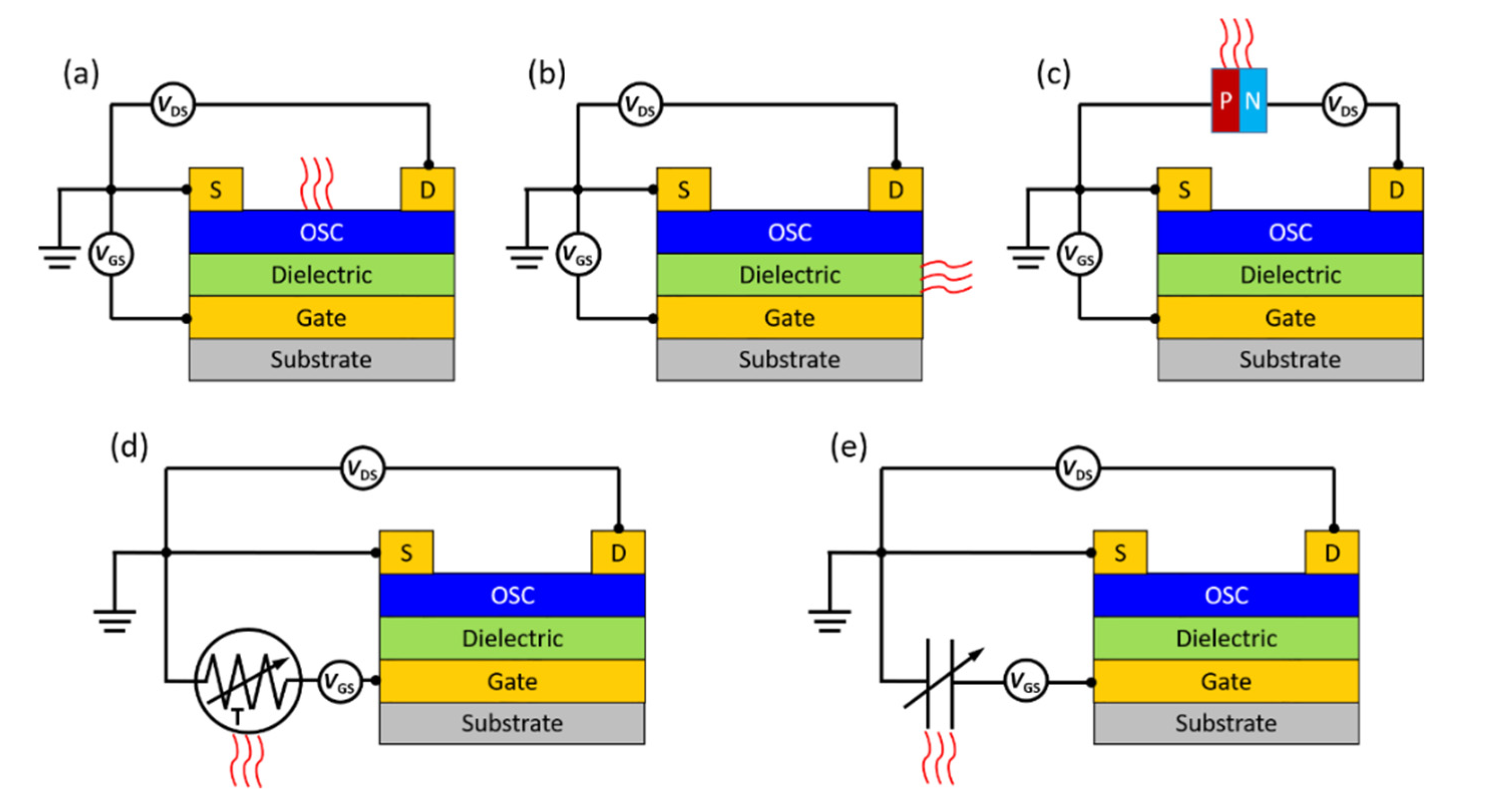
Instead of using an OFET component as the sensing element, a separate temperature-sensing element can be integrated with OFET to form an OFET temperature sensor system. For instance, a thermistor is often connected to the gate electrode of the OFET to modulate the OFET I-V characteristics and achieve more sensitive and reliable temperature sensing. Similarly, a capacitor or diode unit can be connected to the OFET as the temperature sensing element to overcome the low sensitivity and complicated temperature response of the OFET active layer. Various representative OFET-based temperature sensors with different sensing elements are schematically shown in Figure 3.
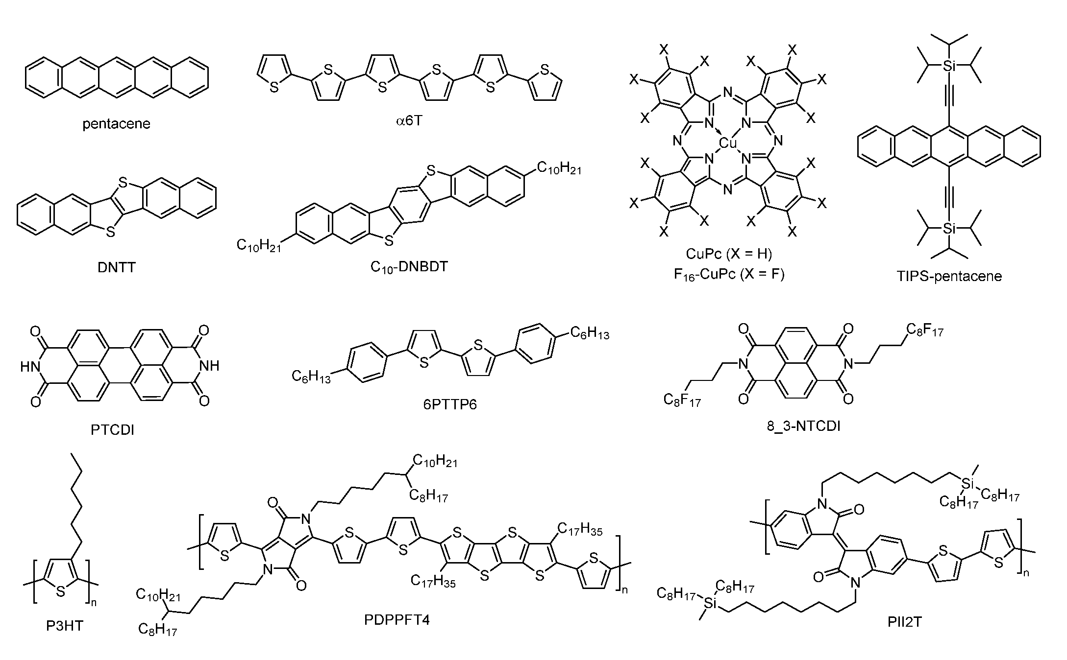
This review aims to introduce and analyze representative studies on OFET temperature sensing devices in terms of materials, device design, and sensing performance. We discuss small-molecule and polymer semiconductors separately, the structures of which are shown in Figure 4. We have classified the device structures by the sensing elements, OFET active layer, dielectric layer, separate thermistor, and other types of sensing elements. Finally, we summarize our findings and provide future prospects on OFET-based temperature sensors. The purpose of this article is to provide readers with a better understanding of the status quo and the challenges that must be overcome before OFET-based temperature sensors can become a viable sensor technology.
2. Small-Molecule Semiconductor-Based OFET Temperature Sensors
Organic small-molecule semiconductors have the advantages of straightforward synthesis, higher purity, and higher charge carrier mobility compared to their polymer counterparts [44,45,46,47]. OFETs based on small-molecule semiconductors have been extensively studied as sensors for various applications such as gas sensor, chemical sensors, biosensors, pressure sensors, etc. [48,49,50]. However, there is a scarcity of research publications on small-molecule-based OFET temperature sensors, presumably due to some of the challenges that will be discussed in this review. Nonetheless, promising results have been obtained through efforts made in the improved materials processing and device design. This section will introduce and discuss small-molecule OFET temperature sensors based on the classification of temperature sensing elements: organic semiconductor channel layer, dielectric layer, separate thermistor, and other types.
2.1. OFET Semiconductor Channel as Sensing Element
Pentacene is one of the most commonly used semiconducting layers in OFET devices for various applications [51,52,53,54]. Jung et al. report an OTFT temperature sensor using pentacene as the semiconducting layer on a flexible polyethylene naphthalate (PEN) film for administering point-of-care diagnoses [39]. A 50 nm pentacene film was deposited on top of a polyvinylphenol (PVP) gate dielectric. When the device is measured between 0 and 80 °C, the IDS increases with increasing temperature. This IDS modulation is mainly due to the positive shift of the VT, so the most significant increase in current is observed in the subthreshold region with a linear increase from ~10−10 A at 0 °C to ~10−8 A at 80 °C.
The same group observed a similar linear IDS-T dependence in the subthreshold region within the range of 0 to 180 °C for a temperature sensor based on pentacene OTFT on a SiO2/Si substrate protected by a polyvinyl alcohol (PVA) mask [55]. IDS in the subthreshold region increases by almost four orders of magnitude with an increase in temperature from 0 to 180 °C. However, a lower VT is required to achieve better sensitivity at the expense of IDS-T linearity. It was found that µsat in the saturation region increases with temperature in the relatively low temperature range of 0 to 60 °C due to the thermally activated hopping transport, which agrees with the trend in the similar temperature range (−13 to 67 °C) observed by Kawakami et al. [56]. The activation energy (Ea) obtained with an Arrhenius fit is 66 meV, indicating a weak dependence of µ on temperature. In the higher temperature range of 60 to 180 °C, µ decreases due to the dominance of carrier scattering at elevated temperatures. As a result, IDS,sat increases slightly with temperature in the range of 0 to 180 °C. The dramatic increase in subthreshold current (IDS,sub) with increasing temperature is mainly due the positive shift of VT. However, VT is affected by the charge traps at the dielectric/semiconductor interface, bias stress, moisture, oxygen, morphology of the semiconductor layer, etc., so it is difficult to use the IDS,sub as a sensor output in practical applications. Therefore, using the more reliable IDS in the saturation region is preferred. However, as previously mentioned, the IDS in the saturation region has a weak dependence on temperature, making it challenging to use as the sensor output.
Copper phthalocyamine (CuPc) and fluorinated copper phthalocyanine (F16CuPc) are widely studied p-type and n-type small-molecule semiconductors for OFETs because of their good carrier mobility and environmental stability. CuPc and F16CuPc exhibit a weak dependence of µsat on temperature around room temperature, each having an Ea of 73 and 39 meV [57,58], respectively, which are similar to that of pentacene [55,56]. Therefore, IDS in the saturation region of OFETs based on these materials would also be weakly dependent on temperature and not suitable as the signal output of temperature sensors around room temperature. Consequently, Boileau et al. used the VT response to the temperature of OFETs based on CuPc and F16-CuPC for DNA sensing [59]. The goal was to design an accurate temperature sensor working in the optimal temperature range (40 to 70 °C) where DNA binding occurs. The authors observed that the hole and electron mobilities (µh and µe) of CuPc and F16CuPc increase with temperature with coefficients of 1%/°C and 0.1%/°C, respectively, in the temperature range of 25 to 90 °C. On the other hand, the VT changes significantly from −7.6 V to −1.8 V with a change rate of 0.11 V/°C for CuPc. For the n-type F16CuPc-based OFET, the VT changes to the negative direction from −9.9 V to −26.4 V with a charge rate of −0.25 V/°C, indicating its better sensitivity than the CuPc device. The opposite VT shift directions and different sensitivities observed for the two semiconductors may be due to their different carriers (holes and electrons) associated with different carrier traps at the interface between the semiconductor and the dielectric.
To improve the temperature sensitivity of F16CuPc-based OFETs, Ye et al. developed an OFET device using a pn heterojunction layer of α-sexithiophene (α6T)/F16CuPC [60]. Specifically, a layer of p-type semiconductor α6T was deposited on top of the F16CuPC semiconducting layer and the source/drain electrodes (Figure 5). It has been reported that the use of a pn heterojunction active channel layer in OFETs can realize ambipolar charge transport characteristics and/or improve charge carrier mobility [61,62,63,64,65]. In particular, the VT is a function of the thickness of the top layer in the pn heterojunction [66], which may allow the use of VT as the sensitivity parameter of the OFET temperature sensor in a more controllable manner. The authors found that when the thickness of the α6T layer increased from 0 nm to ~5–7 nm, VT changed significantly from 23.13 V to 18.10 V, and then stabilized. In the linear regime (|VDS| < |VGS − VT|), the OFET with α6T (20 nm)/F16CuPC (50 nm) displayed a linear log(IDS)-versus-T relationship: in the temperature range of 100 to 300 K (Figure 5a), which is gate voltage dependent. The slope k increases with VGS first, reaching the maximum value of 0.11 dec/°C at VGS = 5 V (most sensitive), and then drops rapidly with further increasing VGS (Figure 5b). As shown in Figure 5c, µ follows a thermally activated Arrhenius behaviour () with two distinct temperature ranges. The activation energy Ea is 40.1 meV above 200 K and drops to 16.3 meV in the lower temperature range of 100 to 200 K. The device also showed linear temperature dependence of VT with different slopes in the two temperature ranges (Figure 5d). In the range of 100 to 200 K, the sensitivity (ΔVT/ΔT) is −0.90 V/°C, and between 200 K and 300 K, the sensitivity is −0.185 V/°C. These two regions are attributed to two different mechanisms dominating in each region. The charge transport in the lower temperature range is dominated by the MTR mechanism, while the charge transport in the higher temperature range is dominated by the thermal enhancement of the hopping transport or VRH. These sensitivities are higher than those of a previously reported OFET with a similar structure with only F16CuPC (−0.02 V/°C) [58], indicating the beneficial effect of using a pn heterojunction structure to improve the sensitivity of the sensor.
An organic–inorganic hybrid perovskite-based ambipolar FET temperature sensor was reported by Haque et al. recently [67]. The active MAPbI3 layer is fabricated using a stoichiometric mixture of powdered methylammonium iodide (MAI) and lead iodide (PbI2). The OTFT exhibited excellent air stability without the need for an encapsulation layer. The charge transport obeys the MTR mechanism where traps, mostly localized in the grain boundaries, have energy levels close to the conduction band, and the trapped electrons can be easily released into the conduction band by thermal energy. The temperature dependence of VT was used as the sensitivity parameter for the device. The VT shows a linear relationship with temperature in the range of 29 to 45 °C with a temperature coefficient value of 200 mV/°C, which is higher than the values reported for inorganic semiconductor-based FET temperature sensors. It was found that maintaining a stoichiometric ratio of MAI and PbI2 is critical to achieving a high sensitivity. The devices with the PbI2-rich and MAI-rich films exhibited much lower temperature coefficients of 12 and 100 mV/°C, respectively, since unreacted PbI2 and MAI can reduce carrier traps.
2.2. OFET Dielectric Layer as Sensing Element
Insulating polymers are often used as dielectric materials in OFETs due to their compatibility with flexible substrates and solution processibility via spin coating, casting, and printing under ambient conditions [68]. Moreover, as with the polymer semiconductors, the structure and functionality of the polymer dielectric can be tuned to meet the requirements of the device. In particular, the properties of some polymer dielectrics are more temperature-dependent than organic semiconductors, so they can be used as sensing elements for OFET temperature sensors.
The 2015 paper by Wu et al. [40] aims to solve the issue with OFET sensor sensitivity at higher temperatures. A common issue with OFET temperature sensors is that above ~300 K the devices show limited thermal sensitivity. This design incorporates a thermoresponsive polar polymer into the dielectric layer of the DNTT-based OFET, which induces interfacial interactions to facilitate charge transport at high temperatures. Polylactide (PLA) was used as the polar material that serves both as a flexible substrate and as a gate dielectric for the device with both n- and p-type small-molecule semiconducting active layers. Specifically, three-arm stereocomplex PLA (tascPLA) was synthesized from the ring-opening polymerization of D-lactide and used for these devices. The MTR mechanism can describe the role that the dielectric plays in temperature sensing. At the interface, PLA induces multiple charge carrier traps with varying energy levels, which decreases the carrier concentration. As the temperature increases, the thermal energy can release carriers from these traps and thus modulate the IDS response. The DNTT-tascPLA-OFET shows a much stronger response in IDS with temperature in the range of 25 to 150 °C compared to the device using SiO2 as the dielectric (Figure 6a,b), indicating the high thermal sensitivity of PLA. The device showed excellent cycling stability at 100 °C (Figure 6c,d). Mobility and VT also show high sensitivities to temperature (Figure 6e,f).
Subbarao et al. used CuPc as the semiconducting layer in conjunction with a tri-layer dielectric system where the polar PVA layer is deposited between a layer of poly(methyl methacrylate) (PMMA) and a layer of Al2O3 [69]. The sensor results displayed two distinct linear trends in the ranges of 240 to 300 K and 300 to 370 K with sensitivities of 0.45 nA/°C and 8 nA/°C, respectively. Below 300 K it can be assumed that the VRH mechanism dominates over the MTR mechanism, while above 300 K the opposite occurs. The device showed quite fast response and recovery times of 25 and 15 s, respectively. The response and recovery times included the time to mechanically switch between temperatures, and the actual sensor response and recovery times are expected to be much faster [69].
Mandal et al. incorporated hexagonal barium titanate nanocrystals (h-BTNCs) as a dielectric film and pentacene as the channel layer to fabricate ultrafast, flexible OFET temperature sensor devices [70]. The perovskite BaTiO3 is a ferroelectric material with its ferroelectric property originated from the crystal structure distortion upon temperature change. The BaTiO3 film synthesized by the traditional high-temperature process is very rough, which will have a negative impact on the current at the semiconductor/dielectric interface. Furthermore, the perovskite BaTiO3 only shows ferroelectric properties at low temperatures. To circumvent these issues, the authors developed a low-temperature (~60 °C) process to prepare h-BTNCs. Thin films of h-BTNCs with very smooth surfaces can be obtained simply by spin coating. A series of OFETs with a bilayer dielectric of h-BTNC (55 nm) on Al2O3 (15 nm), a pentacene semiconductor layer, Cu source, and drain electrodes were fabricated on a thin Al-coated poly(ethylene terephthalate) (PET) substrate (10 μm), where the Al layer is the gate electrode. The devices were encapsulated with a PDMS layer. The OFETs had a low operating voltage of 1.5 V and achieved a high mobility of 1.46 cm2/(V·s). When the device was used as a temperature sensor, it showed a linear dependence of IDS on temperature with a slope (sensitivity) of 20 nA/°C between 27 and 45 °C. The greatly enhanced sensitivity is mainly due to the use of the h-BTNC layer since the contributions of pentacene, and other layers are very small. The flexibility of the device was also evaluated, and the sensor maintained a stable response with a minimal level of hysteresis in the temperature range when subjected to bending with a radius of 4 mm. The device was used to monitor the temperature changes of the air inhaled and exhaled through the nose a few cm from the device. Rapid response and recovery times of 24 and 51 ms, respectively, were achieved.
Rullyani et al. reported the use of poly(N-isopropylacrylamide) (PNIPAM) as a thermoresponsive polymer dielectric for OFET sensors [71]. The PNIPAM layer undergoes reversible phase transitions above its lower critical solution temperature of 32 °C. These transitions enhance the charge transport in the semiconducting layer (pentacene in this case) due to an improved semiconductor/dielectric interface with increasing temperature. The sensor was evaluated between 30 and 45 °C with a sensitivity of 2.58 µA/°C with the IDS being on the order of microamperes. The device is suitable for sensing the human body temperatures.
2.3. Thermistor as Sensing Element
As aforementioned, IDS is a preferred parameter as an output signal of OFET temperature sensors because of its high reliability, but its temperature dependence is weak. On the other hand, VT has strong temperature dependence, but it is affected by numerous factors in the fabrication process and the device operating environment. To solve this issue, thermistors, whose resistance changes notably with temperature, have been integrated with OFETs to make temperature sensors with a high sensitivity.
Ren et al. [42] integrated a thermistor with an OFET to improve the dependence of IDS on temperature (Figure 7), and used dynamic range (DR) to present the sensitivity of the device. The thermistor consists of pentacene film embedded with Ag nanoparticles and two electrodes. One electrode of the thermistor is connected to the gate of the pentacene-based OTFT, so the gate bias of the OFET can be modulated by the resistance of the thermistor. Ag nanoparticles act as charge traps, so the conductivity activation energy of the thermistor film is increased to 361 meV compared with pure pentacene (157 meV). This results in a stronger dependence of the conductivity on the temperature of the thermistor film.
The integrated temperature sensor device shows almost three orders of magnitude increase in IDS with temperature when measured between 15 and 70 °C with a measurement step of 5 °C. The sensitivity of the temperature sensor is represented by the DR, which is the ratio between the maximum and minimum changes of IDS at a specific temperature (T) with reference to the lowest temperature (15 °C): DR = ΔIT,max/ΔIT,min, where ΔIT = IT − I15. A higher DR implies a more sensitive device. This device had a DR of 10 bits (102), which is the highest value reported among organic temperature sensors. The sensitivity of the device deteriorates rapidly above 70 °C, which may be due to the evaporation of water absorbed by the polyvinylpyrrolidone (PVPy) dielectric layer at high temperatures, resulting in a decrease in capacitance.
The same research group reported a flexible low operating power 16 × 16 active-matrix OFET temperature sensor array by adopting a similar device design [72]. A high-performance p-type semiconductor dinaphtho[2,3-b:2′,3′-f]thieno[3,2-b]thiophene (DNTT) was used as the active layer in the OFET device. An Al2O3 dielectric layer was used to decrease leakage current down to ~50 pA. A thermistor consisting of an Ag nanoparticles-doped pentacene film active layer was connected to the DNTT-OFET. The array fabricated on an ultrathin (12 μm) PET substrate can be operated at low voltages below 4 V. In the temperature range between 20 and 100 °C, the array achieved a temperature resolution of 0.4 °C and a TCR of −4.4%/°C. The device maintained its integrity after 10,000 bending cycles, and the array was able to provide excellent 2D spatial resolution. The superb flexibility and durability of the sensor array make it suitable for conformal temperature measurement of objects with irregular and varied surface geometry such as flexible electronic products and human bodies.
Temperature and pressure sensor arrays are of great interest because of their potential for artificial skin applications with spatial resolution. Yokota et al. copolymerized butyl acrylate with octadecyl acrylate P (BA-OA) and added 25% graphite filler particles to fabricate positive temperature coefficient (PTC) thermistor sensors [73]. The PTC sensors were integrated with OFETs to create a 12 × 12 active matrix sensor array on a polyimide substrate, where an anodized aluminum oxide layer modified by a phosphonic acid self-assembled monolayer (SAM) was used as the gate dielectric, and a 30 nm DNTT layer was used as the semiconductor later in OFETs. This ultra-flexible sensor array was able to accurately measure temperature shifts after being placed between two lobes of a live rat lung, where small temperature fluctuations occur due to respiration. The array performed well between 29.8 and 37.0 °C with minimal hysteresis (1 °C) and a spatial resolution of 5 mm. Furthermore, the device had a rapid response time of 100 ms and remained stable for 1800 thermal cycles within the operating temperature range.
A recent work by Ishaku and Gleskova reported a temperature sensor with a DNTT-OFET connected to a commercially available thermistor with a negative temperature coefficient (NTC) [74]. The OFET included a dielectric of aluminum oxide (AlOx) with an octadecylphosphonic acid (C18PA) SAM for low voltage operation. Previous works have reported using C18PA to improve the µsat of charge carriers in OTFTs by inducing edge-on orientation of the semiconducting layer [75]. The integrated OFET-sensor was evaluated between 20 and 50 °C with the thermistor modulating the gate voltage. A low operational voltage of −7 V and a TCR of −2.44%/°C were achieved.
Nakayama et al. reported two types of organic temperature sensing devices using a combination of p- and n-type semiconductors to fabricate analog-to-digital converter (ADC) OFETs [76]. The organic semiconductor layers of 3,11-didecyldinaphtho[2,3-d:2′,3′-d’]benzo[1,2-b:4,5-b’]dithiophene (C10-DNBDT) and GSID 104031-1 (BASF SE) for p- and n-type OFETs, respectively, were solution processed. A unit consisting of a complementary metal oxide semiconductor (CMOS) comparator and an inverter made of the p- and n-channel OFET devices is connected to a temperature sensor unit composed of two PEDOT: PSS resistors (TCR of −0.87%/°C) and two Cr/Au resistors (TCR: 0.064%/°C) to form a temperature detector. The temperature detector can produce a binary digital (1-bit) readout depending on whether the temperature was above a designated threshold value (Tth). The authors further fabricated a 2-bit parallel ADC composed of three comparators and one temperature sensor unit for more detailed temperature detection. The 2-bit ADC can have four output combinations, (0,0,0), (0,0,1), (0,1,1), (1,1,1), corresponding to the temperature ranges of <33 °C, 33–50 °C, 50–67 °C, and >67 °C, respectively. Such digital signals can be easily read with common radio-frequency identification (RFID) readers.
2.4. Other Types of Sensing Elements
Someya et al. reported a large-area network of temperature and pressure sensors on a flexible plastic substrate using organic semiconductors [41]. The temperature sensor cell consists of an organic diode as the temperature sensing element and an OFET. The OFET device is composed of a pentacene semiconductor layer, a polyimide dielectric layer, and Au source, drain, and gate electrodes. The organic diode has a structure of PET/ITO/CuPc (30 nm)/PTCDI (50 nm)/Au, where PTCDI (3,4,9,10-perylenetetracarboxylic diimide) is an n-type semiconductor, forming a pn heterojunction with the p-type CuPc. The pn heterojunction layer has a much stronger temperature dependence than CuPc or PTCDI alone. Therefore, this organic diode functions as a sensing element. The magnitude of IDS of the temperature sensor cell increases markedly from ~0.4 μA to ~1.4 μA in the range of 30 to 80 °C or ~20 nA/°C.
Özgün et al. reported a temperature-responsive array made by integrating pairs of organic semiconductor-based switching diodes and OFETs on a silicon-on-insulator (SOI) wafer, where pentacene was used as the semiconductor in both components [77]. When two OFETs with different sizes are driven, the voltage drop on their diodes is measured at different temperatures. The difference in voltage drop between two diodes is plotted against temperature between 27.2 and 59.0 °C. Below 35 °C, the data shows large deviations, while the rest of the data from 35.0 to 59.0 °C shows a linear trend with a sensitivity of 16.3 mV/°C. The device fabrication is relatively simple and compatible with common microfabrication processes.
Developing polymer composites is a method to improve electrical properties of polymer materials. The interactions between the polymer and the organic/inorganic material in the polymer matrix can lead to higher sensitivity and better overall performance in sensors [78]. Polymer materials can also be used as a matrix to embed active materials to take advantage of polymer properties, such as processability and stability, for organic electronic applications. In 2009, Graz et al. [79] incorporated lead titanate (PbTiO3) nanoparticles into the matrix of ferroelectric P (VDF-TrFE). A two-step polarization process is used to polarize the foil made of this composite material, so that some areas of the PbTO3 nanoparticles and the polymer matrix have parallel polarization directions, while other areas have anti-parallel polarization directions. Areas with parallel polarization directions are pyroelectric, while areas with anti-parallel polarization directions are piezoelectric. The composite foil was laminated to amorphous silicon (a-Si) TFTs on their polyimide gate dielectric substrate in the adjacent parallel and anti-parallel polarization directions, respectively. The IDS of a TFT is modulated pyro- or piezoelectrically depending on the polarization directions of the composite foil area. The device significantly reduced cross-sensitivity between the piezoelectric and pyroelectric effects and displayed a linear relationship correlated to temperature.
Sensor devices can be connected to one of the electrodes of an OFET and their response to the target analyte can be used to modulate a characteristic of the OFET device that changes the output signal of the OFET. In 2014, Cosseddu et al. introduced a temperature sensor based on an organic charge modulated field effect transistor (OCMFET) using the pyroelectric poly(vinylidene difluoride) (PVDF) [43]. The polymer film forms the dielectric layer of a parallel plate capacitor, which is connected to the floating gate of an OFET device. Temperature modulations affect the charge separation in the PVDF layer, which modulates the carrier concentration that directly correlates the IDS response of the sensor. Calibration curves of ΔIDS–T for this temperature sensor were established within a working range of 10 to 42 °C.
Table 1 summarizes the OFET-based temperature sensors using the small-molecule materials discussed in this section organized by sensing the elements and reporting the OFET channel material, working range, output signal, and the reported sensitivity of each device.
3. Polymer Semiconductor-Based OFET Temperature Sensors
Compared to small-molecule materials, polymeric semiconductors have much better solution processability and mechanical strength and are widely used in organic electronics such as OFETs, organic light emitting diodes (OLEDs), organic solar cells, and various other applications [80,81,82,83,84,85].
Polythiophenes are among the earliest and most-studied polymer semiconductors for OFETs [86,87,88,89]. In 1993, Ohmori et al. fabricated Schottky gated OFET devices using poly(3-alkylthiophene)s with different alkyl side chains as the semiconducting layer for temperature sensors [90]. Poly(3-ethylthiophene) (P3ET) demonstrated the best response to temperature changes in the range of 14 to 75 °C when measured in the saturation region. The charge carrier mobilities were evaluated to be 0.0004 cm2/V and 0.006 cm2/V at the high and low temperatures of 14 °C and 75 °C, respectively. This confirmed that the charge transport of P3ET obeys the VRH theory, where a higher temperature augments the probability of hopping transport events, leading to higher carrier mobility. Song et al. reported the use of a poly(3-hexylthiophene) (P3HT)-based OFET as a temperature sensor [91]. The P3HT film was deposited on top of a PMMA dielectric layer with a bottom ITO gate electrode. The IDS increases linearly with temperature in the range between 25 and 100 °C. The authors used the hole mobility temperature coefficient Δμh/ΔT = 2.34 × 10⁻⁵ cm2/V·s·°C to assess the thermal sensitivity of the device. In a 2019 study, Zhu et al. used crosslinked polystyrene-block-poly(ethylene-ran-butylene)-block-polystyrene (SEBS) as the dielectric material and PDPPFT4 or poly(isoindigo-bithiophene) (PII2T) as the semiconductor channel layer in OFETs [92]. The devices showed a linear relationship in the response of IDS to temperature changes between 25 and 55 °C. Devices with PDPPFT4 and PII2T showed TCRs of −2.89%/°C and −4.23%/°C, respectively. The hysteresis effect was negligible for both sensors due to the use of the non-polar gate dielectric. The sensors remained stable after 50 cycles under a 30% uniaxial strain, indicating their excellent stretchability.
The 2017 work from Zhao et al. developed a thermoelectric-gated transistor using P3HT as the active layer for temperature sensing [93]. The architecture of the electrolyte-gated transistor (EGT) is shown in Figure 8a. Poly(vinylphosphonic acid-co-acrylic acid) P(VPA-AA) was used as a polyanionic electrolyte insulating layer. An applied negative gate bias induces charge separation, forming two electrical double layers (EDLs) (or Helmholtz layers), where positive protons accumulated at the electrolyte/gate interface, while the negative anions accumulated at the semiconductor/electrolyte interface. The two EDLs are separated by only a few angstroms, resulting in a large capacitance. This device is then connected to the working electrode of an ionic thermoelectric supercapacitor (ITESC) containing an NaOH-containing poly(ethyleneoxide) (PEO-NaOH) electrolyte (Figure 8b). A temperature gradient (ΔT) between the two electrodes of the ITESC causes ions to diffuse to the opposite poles, creating an open voltage (Vthermal) between the two electrodes. The Vthermal is used to bias the gate of the transistor, and thus the IDS response is directly dependant on ΔT. The thermal transconductance (gthermal) is defined for the ionic thermoelectric-gated transistor as gthermal = ΔIDS/SΔT, where ΔIDS is the change in IDS caused by the temperature change ΔT, and S is the ionic Seebeck coefficient of PEO-NaOH. Therefore, gthermal can represent the thermal sensitivity of the device. The ionic Seebeck coefficient (S) of PEO-NaOH is found to be as high as 11 mV/°C, which is much higher than that of traditional thermoelectric materials (~100 μV/°C). Hence, higher sensitivity can be achieved for this thermoelectric-gated organic transistor compared to the devices using traditional thermoelectric materials. Interestingly, the authors found that the type of gate material used affects the transfer characteristics of the transistor. When a high work function metal Cu (4.3 eV) is used as the gate, it is easier to turn on the transistor than the device using a low-work function metal Ti (3.8 eV) as the gate. Consequently, the Cu-gated transistor can detect a small ΔT as low as 1 °C, while the Ti-gated transistor requires a minimum ΔT of 3.8 °C to obtain an appreciable IDS. This device displayed negligible hysteresis and fast response time (25–50 s) in the working range of 15 to 45 °C. It should be noted that the response time is rather limited by the response of the thermoelectric component, and not by the ionic thermoelectric-gated transistor. A simple resistor-load heat-gated invertor was fabricated, which can be switched around ΔT = 0 with only 20 °C variation. A maximum gain of eight was achieved. This is the first demonstration that heat signal can be used as the input for logic circuits.
Table 2 summarizes the polymer semiconductor-based OFET temperature sensors discussed in this section.
4. Conclusions and Outlook
Due to the high demand for a large amount of flexible, thin, lightweight, and ultralow-cost sensors for applications in wearable electronics, Internet of Things, smart packaging, advanced healthcare, etc., there is growing interest in the development of sensors using organic semiconductor materials. OFET-based sensors have attracted special attention due to their ability to process on flexible substrates, for seamless integration with other components of the electronic device, and to reduce cross-sensitivity and achieve multi-detection. This review presented the progress made in the development of OFET-based temperature sensors, which have the broadest and most important applications among all types of sensors. We divided the OFET-based sensors by the organic semiconductor channel materials into two groups: small molecules and polymers. The devices are further classified by the sensing element: OFET semiconductor channel, OFET dielectric layer, separate thermistor, and other types. Notable advances have been made in the development of OFET-based temperature sensors, which include the demonstration of high sensitivity (e.g., TCR > 2%/°C), excellent mechanical flexibility and stability, elimination of cross-sensitivity, and successful integration of OFET temperature sensors with other electronic devices. These developments show the potential of OFET sensors in the above-mentioned emerging applications.
Nevertheless, the authors found that compared to the abundance of organic semiconductor materials developed for other organic electronics and the large number of studies on temperature-variable charge transports of organic semiconductors, research on OFETs as temperature sensors is significantly less. This may be because the applications of these sensors have only emerged recently, but the complicated and largely material- and device-dependent charge transport mechanism for organic semiconductors appears to be a more important factor. Specifically, the use of VT, IDS, or other parameters in the linear regime of the OFET as the sensor readout can provide high sensitivity. However, these parameters are extremely sensitive to the trap density in the channel material and dielectric and at their interface, which changes significantly with tiny changes in processing conditions and the environment. The IDS in the saturation regime is a more robust output signal, but its temperature dependence is usually too weak for most organic semiconductors.
Since few organic semiconductors have been studied for OFET temperature sensors, further efforts are required to investigate more organic semiconductors in order to gain a better understanding of the relationship between the chemical structure and the temperature dependency of OFET parameters. Furthermore, material processing and device fabrication for OFET temperature sensors need to be more rigorously controlled and optimized compared to other types of applications. In addition, it is necessary to specifically design new materials with the required characteristics of OFET temperature sensors, such as high sensitivity, easy control of film quality, and less susceptibility to other stimuli in the environment. In particular, the above-mentioned temperature sensors are typically used around the room temperature or near-body temperature (0 to 50 °C). However, most of the known organic semiconductors undergo drastic changes in the charge transport mechanism, causing severe attenuation of the temperature dependence of the conductivity in this temperature range. Innovative design of organic semiconductor materials is needed to solve this problem.
Using the dielectric layer as the sensing element is an effective way to increase the sensitivity and overcome some of the issues with the devices using the channel-sensing layer. However, a high-quality and stable semiconductor channel layer is still needed to make full use of this approach. Many studies have used a separate sensing element, such as a thermistor or a capacitor, to couple to the OFET unit, which is probably the easiest and fastest way to develop OFET-based temperature sensor products. However, the temperature sensing of this type of devices is based on the two terminal sensing elements and, therefore, the devices are less intelligent than the three-terminal OFET sensors using the channel or the dielectric layer as the sensor element. For instance, they may have the cross-sensitivity issue.
Overall, there have been remarkable advances in the development of OFET temperature sensors, which gives an optimistic outlook on the manufacture of flexible and inexpensive OFET temperature sensors for practical use.
Author Contributions
Conceptualization, Y.L.; Writing—Original Draft Preparation, J.P., D.A. and J.H.L.N.; Writing—Review & Editing, J.P., D.A., J.H.L.N. and Y.L.; Supervision, Y.L.; Funding Acquisition, Y.L. All authors have read and agreed to the published version of the manuscript.
Funding
This research was funded by the Natural Sciences and Engineering Research Council of Canada (NSERC) through the Strategic Partnership Grants for Networks (SPG-N), grant number NETGP 508526-17, and the Discovery Grants, grant number RGPIN-2016-04366.
Institutional Review Board Statement
Not applicable.
Informed Consent Statement
Not applicable.
Data Availability Statement
Not applicable.
Conflicts of Interest
The authors declare no conflict of interest.
References
- Klauk, H. Organic Thin-Film Transistors. Chem. Soc. Rev. 2010, 39, 2643. [Google Scholar] [CrossRef]
- Huang, Y.; Kramer, E.J.; Heeger, A.J.; Bazan, G.C. Bulk Heterojunction Solar Cells: Morphology and Performance Relationships. Chem. Rev. 2014, 114, 7006–7043. [Google Scholar] [CrossRef]
- van de Burgt, Y.; Melianas, A.; Keene, S.T.; Malliaras, G.; Salleo, A. Organic Electronics for Neuromorphic Computing. Nat. Electron. 2018, 1, 386–397. [Google Scholar] [CrossRef]
- Lee, Y.H.; Kweon, O.Y.; Kim, H.; Yoo, J.H.; Han, S.G.; Oh, J.H. Recent Advances in Organic Sensors for Health Self-Monitoring Systems. J. Mater. Chem. C 2018, 6, 8569–8612. [Google Scholar] [CrossRef]
- Wang, W.; Zhao, W.; Xu, H.; Liu, S.; Huang, W.; Zhao, Q. Fabrication of Ultra-Thin 2D Covalent Organic Framework Nanosheets and Their Application in Functional Electronic Devices. Coord. Chem. Rev. 2021, 429, 213616. [Google Scholar] [CrossRef]
- Freund, R.; Zaremba, O.; Arnauts, G.; Ameloot, R.; Skorupskii, G.; Dincă, M.; Bavykina, A.; Gascon, J.; Ejsmont, A.; Goscianska, J.; et al. The Current Status of MOF and COF Applications. Angew. Chem. Int. Ed. 2021, 60, 23975–24001. [Google Scholar] [CrossRef]
- Elkington, D.; Cooling, N.; Belcher, W.; Dastoor, P.C.; Zhou, X. Organic Thin-Film Transistor (OTFT)-Based Sensors. Electronics 2014, 3, 234–254. [Google Scholar] [CrossRef] [Green Version]
- Inal, S.; Malliaras, G.G.; Rivnay, J. Benchmarking Organic Mixed Conductors for Transistors. Nat. Commun. 2017, 8, 1767. [Google Scholar] [CrossRef] [Green Version]
- Lee, M.Y.; Lee, H.R.; Park, C.H.; Han, S.G.; Oh, J.H. Organic Transistor-Based Chemical Sensors for Wearable Bioelectronics. Acc. Chem. Res. 2018, 51, 2829–2838. [Google Scholar] [CrossRef]
- Wang, N.; Yang, A.; Fu, Y.; Li, Y.; Yan, F. Functionalized Organic Thin Film Transistors for Biosensing. Acc. Chem. Res. 2019, 52, 277–287. [Google Scholar] [CrossRef]
- Fang, X.; Zong, B.; Mao, S. Metal–Organic Framework-Based Sensors for Environmental Contaminant Sensing. Nano-Micro Lett. 2018, 10, 64. [Google Scholar] [CrossRef] [Green Version]
- Urban, G.; Jachimowicz, A.; Kohl, F.; Kuttner, H.; Olcaytug, F.; Kamper, H.; Pittner, F.; Mann-Buxbaum, E.; Schalkhammer, T.; Prohaska, O.; et al. High-Resolution Thin-Film Temperature Sensor Arrays for Medical Applications. Sens. Actuators A Phys. 1990, 22, 650–654. [Google Scholar] [CrossRef]
- Khan, Y.; Ostfeld, A.E.; Lochner, C.M.; Pierre, A.; Arias, A.C. Monitoring of Vital Signs with Flexible and Wearable Medical Devices. Adv. Mater. 2016, 28, 4373–4395. [Google Scholar] [CrossRef]
- Mansor, H.; Shukor, M.H.A.; Meskam, S.S.; Rusli, N.Q.A.M.; Zamery, N.S. Body Temperature Measurement for Remote Health Monitoring System. In Proceedings of the 2013 IEEE International Conference on Smart Instrumentation, Measurement and Applications (ICSIMA), Kuala Lumpur, Malaysia, 25–27 November 2013; pp. 1–5. [Google Scholar]
- Harada, S.; Kanao, K.; Yamamoto, Y.; Arie, T.; Akita, S.; Takei, K. Fully Printed Flexible Fingerprint-like Three-Axis Tactile and Slip Force and Temperature Sensors for Artificial Skin. ACS Nano 2014, 8, 12851–12857. [Google Scholar] [CrossRef]
- Kanao, K.; Harada, S.; Yamamoto, Y.; Honda, W.; Arie, T.; Akita, S.; Takei, K. Highly Selective Flexible Tactile Strain and Temperature Sensors against Substrate Bending for an Artificial Skin. RSC Adv. 2015, 5, 30170–30174. [Google Scholar] [CrossRef]
- Mansoor, M.; Haneef, I.; Akhtar, S.; De Luca, A.; Udrea, F. Silicon Diode Temperature Sensors—A Review of Applications. Sens. Actuators A Phys. 2015, 232, 63–74. [Google Scholar] [CrossRef]
- Newman, C.R.; Frisbie, C.D.; da Silva Filho, D.A.; Brédas, J.-L.; Ewbank, P.C.; Mann, K.R. Introduction to Organic Thin Film Transistors and Design of N-Channel Organic Semiconductors. Chem. Mater. 2004, 16, 4436–4451. [Google Scholar] [CrossRef]
- Zaumseil, J.; Sirringhaus, H. Electron and Ambipolar Transport in Organic Field-Effect Transistors. Chem. Rev. 2007, 107, 1296–1323. [Google Scholar] [CrossRef]
- Schafft, H.A.; Suehle, J.S. The Measurement, Use and Interpretation of the Temperature Coefficient of Resistance of Metallizations. Solid-State Electron. 1992, 35, 403–410. [Google Scholar] [CrossRef]
- Torsi, L.; Dodabalapur, A.; Sabbatini, L.; Zambonin, P.G. Multi-Parameter Gas Sensors Based on Organic Thin-Film-Transistors. Sens. Actuators B 2000, 67, 312–316. [Google Scholar] [CrossRef]
- Poghossian, A.; Schultze, J.W.; Schöning, M.J. Multi-Parameter Detection of (Bio-)Chemical and Physical Quantities Using an Identical Transducer Principle. Sens. Actuators B Chem. 2003, 91, 83–91. [Google Scholar] [CrossRef]
- Horowitz, G. Organic Field-Effect Transistors. Adv. Mater. 1998, 10, 365–377. [Google Scholar] [CrossRef]
- Stallinga, P. Electronic Transport in Organic Materials: Comparison of Band Theory with Percolation/(Variable Range) Hopping Theory. Adv. Mater. 2011, 23, 3356–3362. [Google Scholar] [CrossRef]
- Coropceanu, V.; Cornil, J.; da Silva Filho, D.A.; Olivier, Y.; Silbey, R.; Brédas, J.-L. Charge Transport in Organic Semiconductors. Chem. Rev. 2007, 107, 926–952. [Google Scholar] [CrossRef]
- Mei, Y.; Diemer, P.J.; Niazi, M.R.; Hallani, R.K.; Jarolimek, K.; Day, C.S.; Risko, C.; Anthony, J.E.; Amassian, A.; Jurchescu, O.D. Crossover from Band-like to Thermally Activated Charge Transport in Organic Transistors Due to Strain-Induced Traps. Proc. Natl. Acad. Sci. USA 2017, 114, E6739–E6748. [Google Scholar] [CrossRef] [Green Version]
- Lee, J. Physical Modeling of Charge Transport in Conjugated Polymer Field-Effect Transistors. J. Phys. D Appl. Phys. 2021, 54, 143002. [Google Scholar] [CrossRef]
- de Boer, R.W.I.; Gershenson, M.E.; Morpurgo, A.F.; Podzorov, V. Organic Single-Crystal Field-Effect Transistors. Phys. Status Solidi A 2004, 201, 1302–1331. [Google Scholar] [CrossRef] [Green Version]
- Minder, N.A.; Ono, S.; Chen, Z.; Facchetti, A.; Morpurgo, A.F. Band-Like Electron Transport in Organic Transistors and Implication of the Molecular Structure for Performance Optimization. Adv. Mater. 2012, 24, 503–508. [Google Scholar] [CrossRef] [Green Version]
- Yamashita, Y.; Tsurumi, J.; Hinkel, F.; Okada, Y.; Soeda, J.; Zajączkowski, W.; Baumgarten, M.; Pisula, W.; Matsui, H.; Müllen, K.; et al. Transition Between Band and Hopping Transport in Polymer Field-Effect Transistors. Adv. Mater. 2014, 26, 8169–8173. [Google Scholar] [CrossRef]
- Rani, V.; Kumar, P.; Sharma, A.; Yadav, S.; Singh, B.; Ray, N.; Ghosh, S. Carrier Induced Hopping to Band Conduction in Pentacene. Sci. Rep. 2019, 9, 20193. [Google Scholar] [CrossRef]
- Senanayak, S.P.; Ashar, A.Z.; Kanimozhi, C.; Patil, S.; Narayan, K.S. Room-Temperature Bandlike Transport and Hall Effect in a High-Mobility Ambipolar Polymer. Phys. Rev. B 2015, 91, 115302. [Google Scholar] [CrossRef] [Green Version]
- Lee, J.; Chung, J.W.; Kim, D.H.; Lee, B.-L.; Park, J.-I.; Lee, S.; Häusermann, R.; Batlogg, B.; Lee, S.-S.; Choi, I.; et al. Thin Films of Highly Planar Semiconductor Polymers Exhibiting Band-like Transport at Room Temperature. J. Am. Chem. Soc. 2015, 137, 7990–7993. [Google Scholar] [CrossRef]
- Schott, S.; Gann, E.; Thomsen, L.; Jung, S.; Lee, J.; McNeill, C.R.; Sirringhaus, H. Charge--Transport Anisotropy in a Uniaxially Aligned Diketopyrrolopyrrole--Based Copolymer. Adv. Mater. 2015, 27, 7356–7364. [Google Scholar] [CrossRef] [Green Version]
- Yamashita, Y.; Hinkel, F.; Marszalek, T.; Zajaczkowski, W.; Pisula, W.; Baumgarten, M.; Matsui, H.; Müllen, K.; Takeya, J. Mobility Exceeding 10 cm2/(V·s) in Donor–Acceptor Polymer Transistors with Band-like Charge Transport. Chem. Mater. 2016, 28, 420–424. [Google Scholar] [CrossRef]
- Podzorov, V.; Menard, E.; Borissov, A.; Kiryukhin, V.; Rogers, J.A.; Gershenson, M.E. Intrinsic Charge Transport on the Surface of Organic Semiconductors. Phys. Rev. Lett. 2004, 93, 086602. [Google Scholar] [CrossRef] [PubMed] [Green Version]
- Merlo, J.A.; Frisbie, C.D. Field Effect Transport and Trapping in Regioregular Polythiophene Nanofibers. J. Phys. Chem. B 2004, 108, 19169–19179. [Google Scholar] [CrossRef]
- Hulea, I.N.; Fratini, S.; Xie, H.; Mulder, C.L.; Iossad, N.N.; Rastelli, G.; Ciuchi, S.; Morpurgo, A.F. Tunable Fröhlich Polarons in Organic Single-Crystal Transistors. Nat. Mater. 2006, 5, 982–986. [Google Scholar] [CrossRef] [PubMed]
- Jung, S.; Ji, T.; Varadan, V.K. Point-of-Care Temperature and Respiration Monitoring Sensors for Smart Fabric Applications. Smart Mater. Struct. 2006, 15, 1872–1876. [Google Scholar] [CrossRef]
- Wu, X.; Ma, Y.; Zhang, G.; Chu, Y.; Du, J.; Zhang, Y.; Li, Z.; Duan, Y.; Fan, Z.; Huang, J. Thermally Stable, Biocompatible, and Flexible Organic Field-Effect Transistors and Their Application in Temperature Sensing Arrays for Artificial Skin. Adv. Funct. Mater. 2015, 25, 2138–2146. [Google Scholar] [CrossRef]
- Someya, T.; Kato, Y.; Sekitani, T.; Iba, S.; Noguchi, Y.; Murase, Y.; Kawaguchi, H.; Sakurai, T. Conformable, Flexible, Large-Area Networks of Pressure and Thermal Sensors with Organic Transistor Active Matrixes. Proc. Natl. Acad. Sci. USA 2005, 102, 12321–12325. [Google Scholar] [CrossRef] [Green Version]
- Ren, X.; Chan, P.K.L.; Lu, J.; Huang, B.; Leung, D.C.W. High Dynamic Range Organic Temperature Sensor. Adv. Mater. 2013, 25, 1291–1295. [Google Scholar] [CrossRef]
- Cosseddu, P.; Viola, F.; Lai, S.; Raffo, L.; Bonfiglio, A. A Temperature Transducer Based on a Low-Voltage Organic Thin-Film Transistor Detecting Pyroelectric Effect. IEEE Electron Device Lett. 2014, 35, 1296–1298. [Google Scholar] [CrossRef]
- Yang, S.Y.; Kim, S.H.; Shin, K.; Jeon, H.; Park, C.E. Low-Voltage Pentacene Field-Effect Transistors with Ultrathin Polymer Gate Dielectrics. Appl. Phys. Lett. 2006, 88, 173507. [Google Scholar] [CrossRef] [Green Version]
- Yamamoto, T.; Takimiya, K. Facile Synthesis of Highly π-Extended Heteroarenes, Dinaphtho[2,3-b:2‘,3‘-f]Chalcogenopheno[3,2-b]Chalcogenophenes, and Their Application to Field-Effect Transistors. J. Am. Chem. Soc. 2007, 129, 2224–2225. [Google Scholar] [CrossRef]
- Takimiya, K.; Shinamura, S.; Osaka, I.; Miyazaki, E. Thienoacene-Based Organic Semiconductors. Adv. Mater. 2011, 23, 4347–4370. [Google Scholar] [CrossRef] [PubMed]
- Quinn, J.T.E.; Zhu, J.; Li, X.; Wang, J.; Li, Y. Recent Progress in the Development of N-Type Organic Semiconductors for Organic Field Effect Transistors. J. Mater. Chem. C 2017, 5, 8654–8681. [Google Scholar] [CrossRef]
- Lin, P.; Yan, F. Organic Thin-Film Transistors for Chemical and Biological Sensing. Adv. Mater. 2012, 24, 34–51. [Google Scholar] [CrossRef]
- Li, H.; Shi, W.; Song, J.; Jang, H.-J.; Dailey, J.; Yu, J.; Katz, H.E. Chemical and Biomolecule Sensing with Organic Field-Effect Transistors. Chem. Rev. 2019, 119, 3–35. [Google Scholar] [CrossRef]
- Yuvaraja, S.; Nawaz, A.; Liu, Q.; Dubal, D.; Surya, S.G.; Salama, K.N.; Sonar, P. Organic Field-Effect Transistor-Based Flexible Sensors. Chem. Soc. Rev. 2020, 49, 3423–3460. [Google Scholar] [CrossRef]
- Baeg, K.-J.; Noh, Y.-Y.; Ghim, J.; Kang, S.-J.; Lee, H.; Kim, D.-Y. Organic Non-Volatile Memory Based on Pentacene Field-Effect Transistors Using a Polymeric Gate Electret. Adv. Mater. 2006, 18, 3179–3183. [Google Scholar] [CrossRef]
- Schroeder, R.; Majewski, L.A.; Grell, M. A Study of the Threshold Voltage in Pentacene Organic Field-Effect Transistors. Appl. Phys. Lett. 2003, 83, 3201–3203. [Google Scholar] [CrossRef]
- Shi, W.; Yu, J.; Katz, H.E. Sensitive and Selective Pentacene-Guanine Field-Effect Transistor Sensing of Nitrogen Dioxide and Interferent Vapor Analytes. Sens. Actuators B Chem. 2018, 254, 940–948. [Google Scholar] [CrossRef]
- Wang, Y.; Kang, L.; Liu, Z.; Wan, Z.; Yin, J.; Gao, X.; Xia, Y.; Liu, Z. Enhancement of Memory Properties of Pentacene Field-Effect Transistor by the Reconstruction of an Inner Vertical Electric Field with an n-Type Semiconductor Interlayer. ACS Appl. Mater. Interfaces 2021, 13, 13452–13458. [Google Scholar] [CrossRef] [PubMed]
- Jung, S.; Ji, T.; Varadan, V.K. Temperature Sensor Using Thermal Transport Properties in the Subthreshold Regime of an Organic Thin Film Transistor. Appl. Phys. Lett. 2007, 90, 062105. [Google Scholar] [CrossRef]
- Kawakami, D.; Yasutake, Y.; Nishizawa, H.; Majima, Y. Bias Stress Induced Threshold Voltage Shift in Pentacene Thin-Film Transistors. Jpn. J. Appl. Phys. 2006, 45, L1127–L1129. [Google Scholar] [CrossRef]
- Kwak, T.H.; Kang, H.S.; Kim, K.; Cho, M.Y.; Lee, J.W.; Joo, J. Copper-Phthalocyanine Based Organic Thin Film Transistor. In Proceedings of the 2006 IEEE Nanotechnology Materials and Devices Conference, Gyeongju, Korea, 22–25 October 2006; pp. 630–631. [Google Scholar]
- Ye, R.; Baba, M.; Ohishi, Y.; Mori, K.; Suzuki, K. On the Correlation between Morphology and Electronic Properties of Fluorinated Copper Phthalocyanine (F16CuPc) Thin Films. Mol. Cryst. Liq. Cryst. 2006, 444, 203–210. [Google Scholar] [CrossRef]
- Boileau, N.T.; Melville, O.A.; Mirka, B.; Cranston, R.; Lessard, B.H. P and N Type Copper Phthalocyanines as Effective Semiconductors in Organic Thin-Film Transistor Based DNA Biosensors at Elevated Temperatures. RSC Adv. 2019, 9, 2133–2142. [Google Scholar] [CrossRef] [Green Version]
- Ye, R.; Ohta, K.; Baba, M. Temperature Dependence of Electrical Properties of Organic Thin Film Transistors Based on Pn Heterojuction and Their Applications in Temperature Sensors. J. Comput. Commun. 2016, 4, 10–15. [Google Scholar] [CrossRef] [Green Version]
- Ye, R.; Baba, M.; Oishi, Y.; Mori, K.; Suzuki, K. Air-Stable Ambipolar Organic Thin-Film Transistors Based on an Organic Homostructure. Appl. Phys. Lett. 2005, 86, 253505. [Google Scholar] [CrossRef]
- Ye, R.; Baba, M.; Suzuki, K.; Mori, K. Improved Performance of Fluorinated Copper Phthalocyanine Thin Film Transistors Using an Organic Pn Junction: Effect of Copper Phthalocyanine Film Thickness. Thin Solid Film. 2009, 517, 3001–3004. [Google Scholar] [CrossRef]
- Wang, J.; Wang, H.; Yan, X.; Huang, H.; Yan, D. Organic Heterojunction and Its Application for Double Channel Field-Effect Transistors. Appl. Phys. Lett. 2005, 87, 093507. [Google Scholar] [CrossRef]
- Xiang, L.; Ying, J.; Han, J.; Zhang, L.; Wang, W. High Reliable and Stable Organic Field-Effect Transistor Nonvolatile Memory with a Poly(4-Vinyl Phenol) Charge Trapping Layer Based on a Pn-Heterojunction Active Layer. Appl. Phys. Lett. 2016, 108, 173301. [Google Scholar] [CrossRef]
- Yu, S.H.; Kang, B.; An, G.; Kim, B.; Lee, M.H.; Kang, M.S.; Kim, H.; Lee, J.H.; Lee, S.; Cho, K.; et al. Pn-Heterojunction Effects of Perylene Tetracarboxylic Diimide Derivatives on Pentacene Field-Effect Transistor. ACS Appl. Mater. Interfaces 2015, 7, 2025–2031. [Google Scholar] [CrossRef] [PubMed]
- Ye, R.; Ohta, K.; Baba, M. In-Situ Study of Pn-Heterojunction Interface States in Organic Thin Film Transistors. Thin Solid Film. 2014, 554, 137–140. [Google Scholar] [CrossRef]
- Haque, F.; Lim, S.; Lee, S.; Park, Y.; Mativenga, M. Highly Sensitive and Ambient Air-Processed Hybrid Perovskite TFT Temperature Sensor. IEEE Electron Device Lett. 2020, 41, 1086–1089. [Google Scholar] [CrossRef]
- Shao, M.; He, Y.; Hong, K.; Rouleau, C.M.; Geohegan, D.B.; Xiao, K. A Water-Soluble Polythiophene for Organic Field-Effect Transistors. Polym. Chem. 2013, 4, 5270. [Google Scholar] [CrossRef]
- Subbarao, N.V.V.; Mandal, S.; Gedda, M.; Iyer, P.K.; Goswami, D.K. Effect of Temperature on Hysteresis of Dipolar Dielectric Layer Based Organic Field-Effect Transistors: A Temperature Sensing Mechanism. Sens. Actuators A Phys. 2018, 269, 491–499. [Google Scholar] [CrossRef]
- Mandal, S.; Banerjee, M.; Roy, S.; Mandal, A.; Ghosh, A.; Satpati, B.; Goswami, D.K. Organic Field-Effect Transistor-Based Ultrafast, Flexible, Physiological-Temperature Sensors with Hexagonal Barium Titanate Nanocrystals in Amorphous Matrix as Sensing Material. ACS Appl. Mater. Interfaces 2019, 11, 4193–4202. [Google Scholar] [CrossRef]
- Rullyani, C.; Singh, M.; Li, S.-H.; Sung, C.-F.; Lin, H.-C.; Chu, C.-W. Stimuli-Responsive Polymer as Gate Dielectric for Organic Transistor Sensors. Org. Electron. 2020, 85, 105818. [Google Scholar] [CrossRef]
- Ren, X.; Pei, K.; Peng, B.; Zhang, Z.; Wang, Z.; Wang, X.; Chan, P.K.L. A Low-Operating-Power and Flexible Active-Matrix Organic-Transistor Temperature-Sensor Array. Adv. Mater. 2016, 28, 4832–4838. [Google Scholar] [CrossRef] [PubMed]
- Yokota, T.; Inoue, Y.; Terakawa, Y.; Reeder, J.; Kaltenbrunner, M.; Ware, T.; Yang, K.; Mabuchi, K.; Murakawa, T.; Sekino, M.; et al. Ultraflexible, Large-Area, Physiological Temperature Sensors for Multipoint Measurements. Proc. Natl. Acad. Sci. USA 2015, 112, 14533–14538. [Google Scholar] [CrossRef] [Green Version]
- Ishaku, A.A.; Gleskova, H. Potential of Low-Voltage Organic Transistors with High on-State Drain Current for Temperature Sensor Development. Org. Electron. 2021, 93, 106152. [Google Scholar] [CrossRef]
- Jang, S.; Son, D.; Hwang, S.; Kang, M.; Lee, S.-K.; Jeon, D.-Y.; Bae, S.; Lee, S.H.; Lee, D.S.; Kim, T.-W. Hybrid Dielectrics Composed of Al2O3 and Phosphonic Acid Self-Assembled Monolayers for Performance Improvement in Low Voltage Organic Field Effect Transistors. Nano Converg. 2018, 5, 20. [Google Scholar] [CrossRef] [PubMed] [Green Version]
- Nakayama, K.; Cha, B.-S.; Kanaoka, Y.; Isahaya, N.; Omori, M.; Uno, M.; Takeya, J. Organic Temperature Sensors and Organic Analog-to-Digital Converters Based on p-Type and n-Type Organic Transistors. Org. Electron. 2016, 36, 148–152. [Google Scholar] [CrossRef]
- Ozgun, R.; Katz, H.E.; Andreou, A.G. Organic Diode Implementations in Configurable Architectures and Temperature Sensors. In Proceedings of the 2013 Microsystems for Measurement and Instrumentation: Fulfilling the Promise (MAMNA), Gaithersburg, MD, USA, 14 May 2013; pp. 24–27. [Google Scholar]
- Dudhe, R.S.; Sinha, J.; Kumar, A.; Rao, V.R. Polymer Composite-Based OFET Sensor with Improved Sensitivity towards Nitro Based Explosive Vapors. Sens. Actuators B Chem. 2010, 148, 158–165. [Google Scholar] [CrossRef]
- Graz, I.; Krause, M.; Bauer-Gogonea, S.; Bauer, S.; Lacour, S.P.; Ploss, B.; Zirkl, M.; Stadlober, B.; Wagner, S. Flexible Active-Matrix Cells with Selectively Poled Bifunctional Polymer-Ceramic Nanocomposite for Pressure and Temperature Sensing Skin. J. Appl. Phys. 2009, 106, 034503. [Google Scholar] [CrossRef]
- Guo, X.; Baumgarten, M.; Müllen, K. Designing π-Conjugated Polymers for Organic Electronics. Prog. Polym. Sci. 2013, 38, 1832–1908. [Google Scholar] [CrossRef]
- Zhou, H.; Yang, L.; You, W. Rational Design of High Performance Conjugated Polymers for Organic Solar Cells. Macromolecules 2012, 45, 607–632. [Google Scholar] [CrossRef] [Green Version]
- Li, W.; Hendriks, K.H.; Wienk, M.M.; Janssen, R.A.J. Diketopyrrolopyrrole Polymers for Organic Solar Cells. Acc. Chem. Res. 2016, 49, 78–85. [Google Scholar] [CrossRef] [Green Version]
- Sekine, C.; Tsubata, Y.; Yamada, T.; Kitano, M.; Doi, S. Recent Progress of High Performance Polymer OLED and OPV Materials for Organic Printed Electronics. Sci. Technol. Adv. Mater. 2014, 15, 034203. [Google Scholar] [CrossRef]
- Pivrikas, A.; Sariciftci, N.S.; Juška, G.; Österbacka, R. A Review of Charge Transport and Recombination in Polymer/Fullerene Organic Solar Cells. Prog. Photovolt. Res. Appl. 2007, 15, 677–696. [Google Scholar] [CrossRef]
- Yeh, N.; Yeh, P. Organic Solar Cells: Their Developments and Potentials. Renew. Sustain. Energy Rev. 2013, 21, 421–431. [Google Scholar] [CrossRef]
- Sirringhaus, H.; Brown, P.J.; Friend, R.H.; Nielsen, M.M.; Bechgaard, K.; Langeveld-Voss, B.M.W.; Spiering, A.J.H.; Janssen, R.A.J.; Meijer, E.W.; Herwig, P.; et al. Two-Dimensional Charge Transport in Self-Organized, High-Mobility Conjugated Polymers. Nature 1999, 401, 685–688. [Google Scholar] [CrossRef]
- Ong, B.S.; Wu, Y.; Liu, P.; Gardner, S. High-Performance Semiconducting Polythiophenes for Organic Thin-Film Transistors. J. Am. Chem. Soc. 2004, 126, 3378–3379. [Google Scholar] [CrossRef]
- Ong, B.S.; Wu, Y.; Li, Y.; Liu, P.; Pan, H. Thiophene Polymer Semiconductors for Organic Thin-Film Transistors. Chem. Eur. J. 2008, 14, 4766–4778. [Google Scholar] [CrossRef] [PubMed]
- McCulloch, I.; Heeney, M.; Bailey, C.; Genevicius, K.; MacDonald, I.; Shkunov, M.; Sparrowe, D.; Tierney, S.; Wagner, R.; Zhang, W.; et al. Liquid-Crystalline Semiconducting Polymers with High Charge-Carrier Mobility. Nat. Mater. 2006, 5, 328–333. [Google Scholar] [CrossRef] [PubMed]
- Ohmori, Y.; Muro, K.; Yoshino, K. Gas-Sensitive and Temperature-Dependent Schottky Gated Field Effect Transistors Utilizing Poly(3-Alkylthiophene)s. Synth. Met. 1993, 57, 4111–4116. [Google Scholar] [CrossRef]
- Song, M.; Seo, J.; Kim, H.; Kim, Y. Flexible Thermal Sensors Based on Organic Field-Effect Transistors with Polymeric Channel/Gate-Insulating and Light-Blocking Layers. ACS Omega 2017, 2, 4065–4070. [Google Scholar] [CrossRef] [Green Version]
- Zhu, C.; Wu, H.-C.; Nyikayaramba, G.; Bao, Z.; Murmann, B. Intrinsically Stretchable Temperature Sensor Based on Organic Thin-Film Transistors. IEEE Electron Device Lett. 2019, 40, 1630–1633. [Google Scholar] [CrossRef]
- Zhao, D.; Fabiano, S.; Berggren, M.; Crispin, X. Ionic Thermoelectric Gating Organic Transistors. Nat. Commun. 2017, 8, 14214. [Google Scholar] [CrossRef] [PubMed] [Green Version]
Figure 1.
Four common OFET architectures: (a) bottom-gate top-contact (BGTC), (b) bottom-gate bottom-contact (BGBC), (c) top-gate top-contact (TGTC), and (d) top-gate bottom-contact (TGBC). Schematic output characteristics and transfer characteristics in the linear and saturation regimes of an OFET device are shown in (e), where VDS is the drain voltage, IDS is the drain current, VGS is the gate voltage, VT is the threshold (gate) voltage, and V0 is the onset (gate) voltage. The red arrows in (a–d) indicate the current flow in the channel.

Figure 2.
Various charge transport mechanisms for organic semiconductors (a) Band-like transport and (b) its corresponding mobility-temperature relationship; (c) Multiple-trap and release and (d) its corresponding mobility-temperature relationship; (e) Variable range hopping and (f) its corresponding mobility-temperature relationship; (g) Bässler’s Gaussian disorder model and (h) its corresponding mobility-temperature relationship; (i) Charge transfer (Marcus) and (j) its corresponding mobility-temperature relationship; (k) Nuclear tunneling and (l) its corresponding mobility-temperature relationship. Reproduced with permission from [36] Royal Society of Chemistry, 2017.

Figure 3.
OFET-based temperature sensors with different sensing elements: (a) OFET active layer [39]; (b) dielectric layer [40]; (c) separate diode (shows the diode direction of the p-channel OFET) [41]; (d) separate thermistor [42]; (e) separate capacitor [43].

Figure 4.
Chemical structures of small-molecule and polymeric semiconductors used for OFET temperature sensors.
Figure 4.
Chemical structures of small-molecule and polymeric semiconductors used for OFET temperature sensors.

Figure 5.
(a) Dependence of log (IDS) on the temperatures at different VGS, (b) dependence of k on VGS in obtained from data in (a), (c) temperature dependence of µ, and (d) temperature dependence of VT of the α6T (20 nm)/F16CuPc (50 nm) OFET device in the linear regime. Reproduced with permission from [60] Scientific Research, 2016. Note: ID and VG in (a) are IDS and VGS, respectively.

Figure 6.
Temperature sensitivity of DNTT-tascPLA-OFETs: (a) transfer characteristics of DNTT-tascPLA-OFET (VDS = −60 V) at different temperatures, (b) normalized (N.M.) IDS at different temperatures of the OFETs with tascPLA or SiO2 dielectric layers, (c) normalized IDS of the DNTT-tascPLA-OFET measured between two temperatures of 25 and 100 °C, (d) IDS of the tascPLA–OFETs maintained at 100 °C as a function of time at VDS = −80 V at two different VGS, and (e) µ and (f) VT of the DNTT-tascPLA-OFETs at different temperatures. Reproduced with permission from [40] Wiley-VCH, 2015.

Figure 7.
(a) The schematic diagram of the transistor–thermistor temperature sensor; (b) The circuit of temperature sensor; (c) IDS response to temperature of the transistor-thermistor device. Reproduced with permission from [42] Wiley-VCH, 2013.
Figure 7.
(a) The schematic diagram of the transistor–thermistor temperature sensor; (b) The circuit of temperature sensor; (c) IDS response to temperature of the transistor-thermistor device. Reproduced with permission from [42] Wiley-VCH, 2013.

Figure 8.
(a) Structure of the electrolyte-gated transistor with a negative bias applied to the gate with the formation of EDLs and the chemical structures of P3HT and P(VPA-AA); (b) Structure of the ionic thermoelectric supercapacitor (ITESC), where positive charges are Na+ cations and negative charges are immobile alkoxylate and carboxylate anions; (c) The transfer characteristics; (d) Transconductance of ionic thermoelectric-gated transistors using Cu and Ti as the gate electrode versus the temperature change (ΔT). Reproduced with permission from [93] Springer Nature, 2017. Note: Vg is VGS.


Table 1.
Summary of of small-molecule OFET temperature sensors.
| Sensor Structure | OFET Channel | Sensing Element | Working Range | Sensor Parameter | Sensitivity | Year [Ref.] |
|---|---|---|---|---|---|---|
| Sensing element: OFET active layer | ||||||
| OFET | Pentacene | OFET channel | 0–80 °C | IDS,sub | ~0.1 nA/°C 1 | 2006 [39] |
| OFET | Pentacene | OFET channel | 0–180 °C | IDS,sub, VT | - | 2007 [55] |
| OFET | CuPc | OFET channel | 25–90 °C | VT | 0.11 V/°C | 2019 [59] |
| OFET | F16CuPc | OFET channel | 25–90 °C | VT | −0.25 V/°C | 2019 [72] |
| OFET | α6T/F16CuPc pn junction | OFET channel | −173–27 °C | VT | −0.090 V/°C (<–73 °C) −0.185 V/°C (>–73 °C) | 2016 [60] |
| Organic-inorganic FET | MAPbI3 | FET channel | 20–45 °C | VT | −200 mV/°C | 2020 [67] |
| Sensing element: dielectric layer | ||||||
| OFET | 6PTTP6 8-3-NTCDI DNTT | Dielectric (PLA) | −25–200 °C | IDS | 0.29 μA/°C 1 | 2015 [40] |
| OFET | CuPc | Dielectric (PVA) | −20–0 °C | IDS | 0.45 nA/°C (<300 K) 8 nA/°C (>300 K) | 2018 [69] |
| OFET | Pentacene | Dielectric (h-BTNC) | 27–45 °C | IDS | 20 nA/°C | 2019 [70] |
| OFET | Pentacene | Dielectric (PNIPAM) | 30–45 °C | IDS | 2.58 µA/°C | 2020 [71] |
| Sensing element: thermistor | ||||||
| OFET-thermistor | Pentacene | Thermistor (Pentacene/AgNPs) | 15–70 °C | IDS | DR = 10 bits | 2013 [42] |
| OFET-thermistor | DNTT | Thermistor (Pentacene/AgNPs) | 20–100 °C | TCR | −4.40%/°C | 2016 [72] |
| OFET-thermistor | DNTT | PTC thermistor (copolymer-graphite) | 29.8–37.0 °C | IDS or R | 20 mK | 2015 [73] |
| OFET-thermistor | DNTT | Thermistor (commercial) | 20–50 °C | TCR | −2.44%/°C | 2021 [74] |
| OFET-thermistor ADC | C10-DNBDT (p) GSID 104031-1 (n) | Thermistors (PEDOT:PSS; Cr/Au) | 33–67 °C | Binary codes | - | 2016 [76] |
| Sensing element: other types | ||||||
| OFET-diode | Pentacene | Diode (CuPc/PTCDI) | 30–80 °C | IDS | ~20 nA/°C | 2005 [41] |
| OFET-diode | Pentacene | OFET& Diode | 27.2–59.0 °C | VDS | 16.3 mV/°C | 2013 [77] |
| OFET-capacitor | Pentacene | Capacitor (polymer composite) | ~r. t. | IDS | ~30 nA/°C 1 | 2009 [79] |
| OFET-capacitor | TIPS | Pyroelectric (PVDF) | 10–42 °C | IDS | ~0.14 μA/°C 1 | 2014 [43] |
1 Estimated.
Table 2.
Summary of polymer semiconductor-based OFET temperature sensors.
| Sensor Structure | OFET Channel | Sensing Element | Working Range | Sensor Parameter | Sensitivity | Year [Ref.] |
|---|---|---|---|---|---|---|
| OFET | P3ET | OFET channel | 14–75 °C | μh | 9 × 10⁻⁵ (cm2/V·s)/°C 1 | 1993 [90] |
| OFET | P3HT | OFET channel | 25–100 °C | μh | 2.34 × 10⁻⁵ (cm2/V·s)/°C | 2017 [91] |
| OFET | PDPPFT4 | OFET channel | 25–55 °C | TCR | –2.89%/°C | 2019 [92] |
| OFET | PII2T | OFET channel | 25–55 °C | TCR | –4.23%/°C | 2019 [92] |
| OFET/capacitor | P3HT | Capacitor (PEO-NaOH) | 15–45 °C | IDS gthermal | 20 nA/°C 0.08 μS/°C 1 | 2017 [93] |
1 Estimated.
Publisher’s Note: MDPI stays neutral with regard to jurisdictional claims in published maps and institutional affiliations. |
© 2021 by the authors. Licensee MDPI, Basel, Switzerland. This article is an open access article distributed under the terms and conditions of the Creative Commons Attribution (CC BY) license (https://creativecommons.org/licenses/by/4.0/).
Share and Cite
MDPI and ACS Style
Polena, J.; Afzal, D.; Ngai, J.H.L.; Li, Y. Temperature Sensors Based on Organic Field-Effect Transistors. Chemosensors 2022, 10, 12. https://0-doi-org.brum.beds.ac.uk/10.3390/chemosensors10010012
AMA Style
Polena J, Afzal D, Ngai JHL, Li Y. Temperature Sensors Based on Organic Field-Effect Transistors. Chemosensors. 2022; 10(1):12. https://0-doi-org.brum.beds.ac.uk/10.3390/chemosensors10010012
Chicago/Turabian StylePolena, John, Daniel Afzal, Jenner H. L. Ngai, and Yuning Li. 2022. "Temperature Sensors Based on Organic Field-Effect Transistors" Chemosensors 10, no. 1: 12. https://0-doi-org.brum.beds.ac.uk/10.3390/chemosensors10010012
Note that from the first issue of 2016, this journal uses article numbers instead of page numbers. See further details here.