
Properties of Composite Powder Based on Boron Nitride Prepared under Concentrated Light


Frantsevich Institute for Problems of Materials Science of NAS of Ukraine, 3 Krzhyzhanovsky Str., 03142 Kiev, Ukraine
*
Author to whom correspondence should be addressed.
Condens. Matter 2022, 7(2), 42; https://0-doi-org.brum.beds.ac.uk/10.3390/condmat7020042
Submission received: 5 May 2022
/
Revised: 5 June 2022
/
Accepted: 8 June 2022
/
Published: 11 June 2022
(This article belongs to the Special Issue Advances in Nanocomposite Materials)
Abstract
:The results of direct synthesis of composite powder based on boron nitride (BN) are considered. Concentrated light heating of the initial boron powder was carried out in a xenon high-flux optical furnace in a nitrogen flow. Formation of particles of the desired sizes and architecture highly dependent of the synthesis conditions. The flow of nitrogen separates the particles depending on their architecture and size. An increase in the distance from the reaction zone leads to the formation of powder with a wider bandgap, increases the amount of amorphous phase, and decreases the amount of oxide in the collected composite powder. However, the close distance to the reaction zone and high temperatures provide a denser packing of the structure on the particle surface and the disappearance of the BN transition phases. Incorporation of the nickel sulfate hexahydrate to initial boron contributes to the formation of graphene-like structures.
1. Introduction
The behavior of individual atoms and electrons becomes important in nanostructures. Quantum effects come into play, and these fundamentally alter the optical, electrical, and magnetic behavior of materials. Nanostructured composite materials based on BN with a wide bandgap and non-magnetism are expected to show promising electronic, optical, and magnetic properties, which are essential for optoelectronic devices such as lasers, photodiodes, and phototransistors [1,2,3].
Wide-bandgap nitride materials and related compounds being investigated extensively find their applications in high-speed optoelectronic devices in the visible and ultraviolet (UV) range of the electromagnetic spectrum. The increasing demand of shorter wavelength (in the UV range) devices for optical storage, environmental protection, and medical treatment is driving researchers to explore new materials with bandgaps higher than that of GaN. One example of wide-bandgap material is hexagonal boron nitride [4].
The recent surge in graphene research has stimulated interest in the investigation of various two-dimensional (2D) nanomaterials. Two-dimensional hexagonal boron nitride (h-BN) nanostructures are the isoelectric analogs to graphene structures, which share very similar structural characteristics along with many physical properties except for the large bandgap. Analogous to graphene, diatomic B−N pairs in single-layer h-BN are packed in a honeycomb structure with sp2—hybridized covalent bonding. The bulk h-BN compound has excellent mechanical and thermal properties and a high chemical stability. In contrast to semi-metallic graphene, h-BN is a wide direct bandgap insulator, which makes it a promising electrically insulating substrate for graphene electronics due to the atomic flatness of h-BN and absence of charge traps on h-BN surface [5]. Quantum-mechanical simulations show that undergoing dramatic changes in electronic bonding of the pertinent structures could cause structural transitions of c-BN in films to the corresponding h-BN [6].
First-principle calculations have demonstrated the effect of stacking behavior of hexagonal basal layers on the structure and electronic properties of h-BN. The mixed stacking behavior in real h-BN crystals is a result of intrinsic stacking faults. Therefore, a large interlayer spacing of the structures in different BN powder can be explained by a stacking disorder. The existence of a substable structure and related intrinsic stacking fault in real h-BN clarify the discrepancy in the nature of the bandgap and the large variation in the observed bandgap values of h-BN [7].
Electron energy-loss spectroscopy reveals the N-rich h-BN layers with a ratio of B/N = 0.75–0.85. Angle-resolved X-ray absorption near edge structure of these two N-rich nanostructures has been compared with that of h-BN microcrystals. The π* transition in the N K-edge shifts to the lower energy by 0.8–1.0 eV from that of h-BN microcrystals, and the second-order signals of N 1s electrons become significant. It was suggested that the N enrichment would decrease the bandgap of nanostructures from that of h-BN microcrystals [8].
The effects of intrinsic defects on the electronic structure of boron–nitrogen nanotubes were also investigated using the method of linearized associated cylindrical waves. Nanotubes with extended defects of substitution N B of a boron atom by a nitrogen atom and, vice versa (nitrogen by boron B N with an impurity concentration of 1.5 to 5%) are considered. It was shown that the presence of such defects significantly affects the band structure of boron–nitrogen nanotubes. A defect band is formed in the bandgap, which sharply reduces the width of the gap. The presence of impurities has also demonstrated effects on the valence band: the widths of s, sp, and p π bands change and the gap between s and sp bands is partially filled. These effects may be detected experimentally by, e.g., optical and photoelectron spectroscopy [9].
Photoluminescent (PL) and optical absorption spectra of high-yield multi-wall BN nanotubes (BNNTs) were systematically investigated at room temperature in comparison with commercial hexagonal BN (h-BN) powder. The direct bandgap of the BNNTs was determined to be 5.75 eV, just slightly narrower than that of h-BN powder (5.82 eV) [10].
Many methods for synthesis BN were reported [11]. At the industrial scale, its fabrication is made by conventional powder technology requiring nitridation or carbothermal reaction of boric acid/boric oxide with melamine or urea and use of additives during the further sintering process [12].
One of the solutions to tailor the nanostructure and architecture of ceramics is development of “ceramic through chemistry” concepts [11]. These concepts will give the opportunity to generate enhanced physical and chemical properties as well as unusual properties through both the control of the composition at the atomic scale in a molecular or polymeric precursor, and through their shaping, allow the design of tailored materials from zero- (0D) to three-dimensional (3D) structures. However, synthesis of a powder based on BN by direct nitriding of boron will reduce the number of different factors which control the composition at the atomic scale, and so can be considered as a model process which will help us to more clearly understand the effect of each of the different experimental factors on the properties of the resulting powder material [13].
Heating of boron under the effect of concentrated light in an optical furnace in a flow of nitrogen is a good example of a model process for synthesis of the powder based on BN, as for as light energy it is one of the cleanest energy sources available. Moreover, an optical furnace has a number of advantages because this technique is suitable for both conducting and non-conducting materials. High heating and cooling rates, versatility, and the ability to adjust the temperature profile along each axis, maximum operating temperatures, and environmental adaptability are the other important advantages.
Therefore, the study of the influence of the synthesis conditions, the initial boron powder, and the catalyst on the bandgap, architecture, phase composition, and infrared spectra of the composite powder based on BN prepared by direct nitriding of boron under concentrated light will allow us to more clearly see the patterns of phase and structure formation during nitriding.
2. Experimental Section
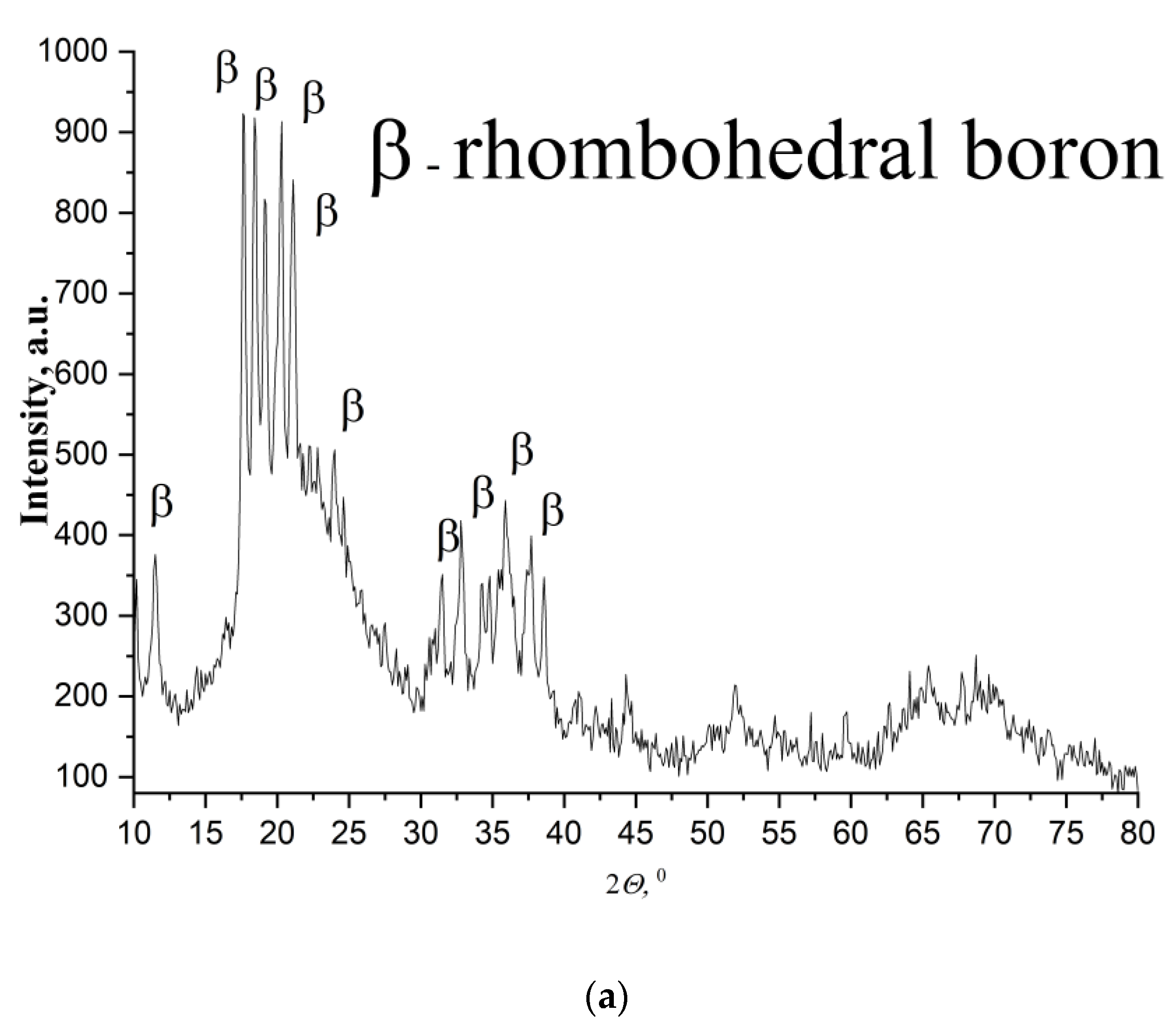
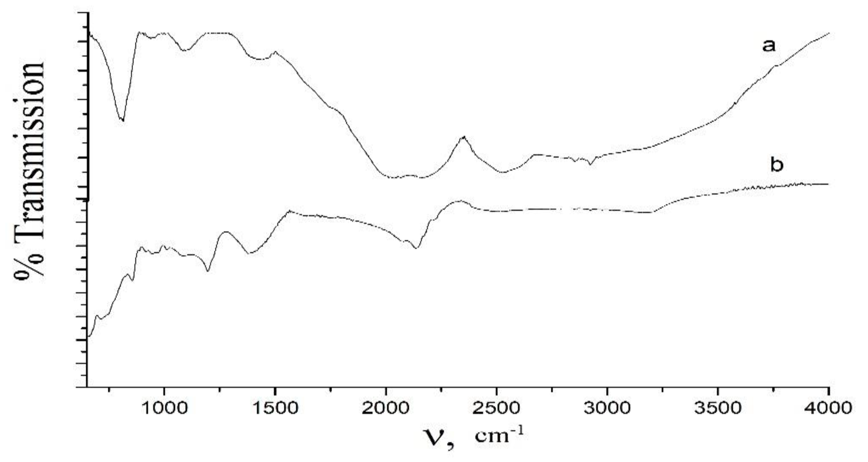
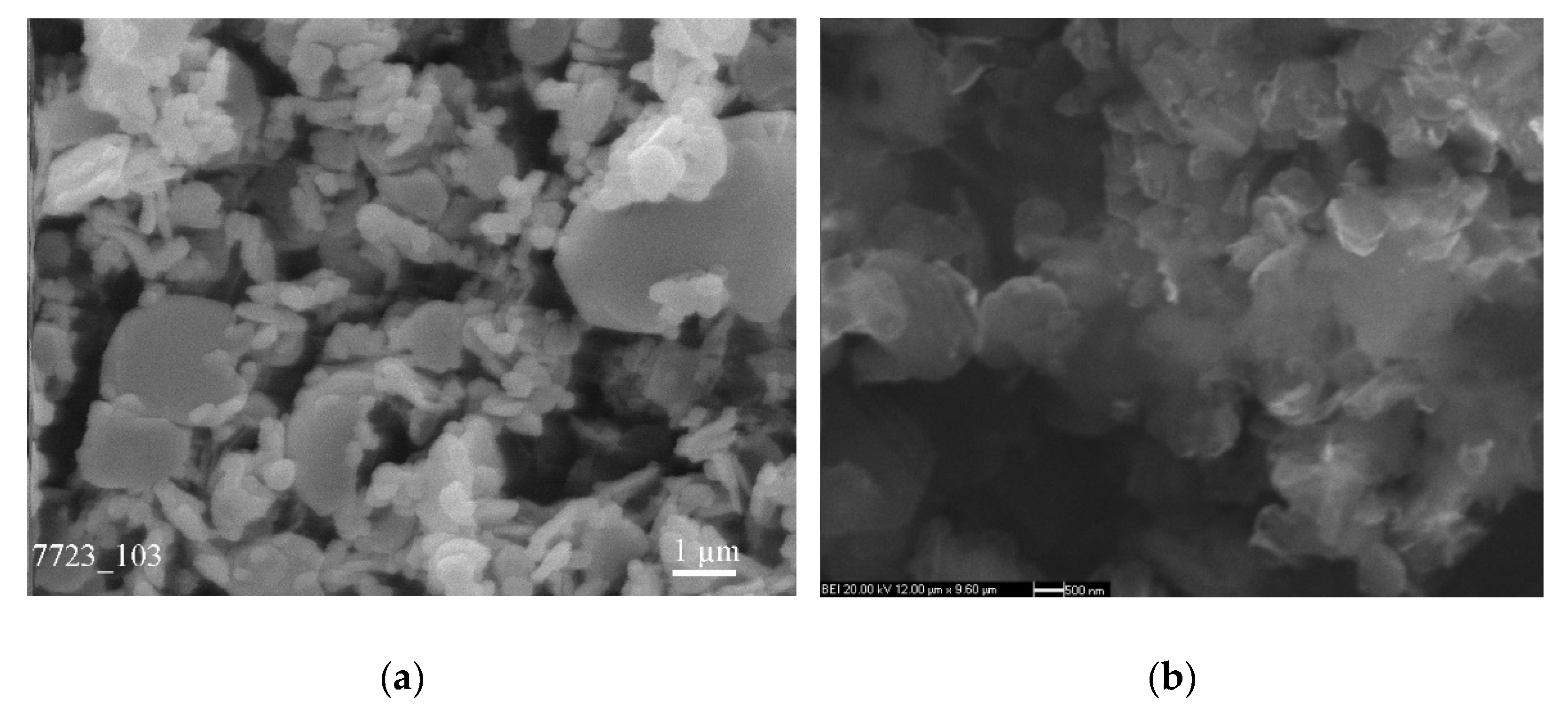
The initial boron powders of a mean particle size—0.05 μm (Figure 1a) and—0.20 μm (Figure 1b) were used as starting powders. Both boron powders are partially amorphous (Figure 2). XRD results proved that β-rhombohedral phase is predominant in the initial boron powder of a mean particle size—0.05 μm (Figure 2a) and is available in the initial boron powder of a mean particle size—0.20 μm (Figure 2b). Main difference between two powders comes from the strong residual B2O3 peaks in phase composition of boron with particle size—0.20 μm (Figure 2b). Negligible impurity of carbon (~B4C) stabilized tetragonal phase of boron in the initial boron powder of a mean particle size—0.20 μm (Figure 2b). Vibrational FTIR spectrum of boron powder of a mean particle size of 0.05 μm confirms its nanostructure, since its transmission over a range 300–1800 cm−1, which characterizes the individual properties of each powder, is significantly higher than that of the initial boron powder of a mean particle size of 0.20 μm (Figure 3).
Heating the surface of the compacted boron powder was carried out in a xenon high-flux optical furnace [14]. A quartz chamber was employed for synthesis of BN powder (Figure 4a). The chamber was flowed with purified and dried nitrogen. Cooper chips heated up to 500 °C purified the nitrogen from oxygen and other pollutions. Platelets of KOH dried the nitrogen from the water. A compacted sample was placed in a focal zone of three xenon emitters on the water-cooled copper screens in the center of the reaction zone (Figure 4b) [15]. BN nanostructures were synthesized at the low-density energy in focal zone of set-up ~0.7 × 10⁴ kW/m2. The time of the experiment was 30 min. Pyrometer measurements showed that the temperature on the side surface of the sample can reach 1450 °C. The temperature in the reaction zone is much higher and can reach above 2000 °C.
During heating of the surface sample, synthesized powder material was deposited on the inner walls and copper screens of the process chamber and was picked up at the surface of the sample, near the reaction zone at the copper screen, at the upper central surface of the chamber, and at its flanges (Figure 4b).
The initial and resulting powders were analyzed using X-ray diffraction (diffractometer “DRON-3.0”, radiation of Kα—Cu). The structure of the powders was examined microstructurally using Superprobe 733, JSM-6490 Scanning Electron Microprobes (JEOL Ltd., Tokyo, Japan). An intercept method was used to estimate the grain size. Infrared spectra of the powders were recorded using Fourier transform infrared spectroscopy Nicolet 6700 FTIR spectrometer equipped with a Thermo Nicole Continuum microscope, a frequency range of 650–4500/cm (Thermo Fisher Scientific, Waltham, MA USA). A detailed spectrophotometric study was performed by spectrophotometer “Specord UV-Vis” (Carl Zeiss Spectroscopy GmbH, Jena, Thüringen, Germany). Exploring the spectral dependence of an optical absorption was carried out on thin films of powdered material, which was precipitated on a quartz substrate.
Nickel sulfate hexahydrate NiSO4.6H2O (KHARKOVTORGSERVIS LLC) was chosen to modify the structure of the composite powder based on BN [16].
3. Results and Discussion
Direct synthesis of the composite powder based on boron nitride from initial boron powder of a mean particle size—0.05 μm in a xenon high-flux optical furnace in a flow of nitrogen results in formation mainly of equiaxed (mean particle size of 0.3 μm) or plate-like particles with thickness of 0.3 μm (mean size of the plate-like surface of a particle of 2.5 μm) on the surface of a compacted sample in close proximity to the reaction zone (Figure 5a). Incorporation of NiSO4·6H2O into initial boron powder of a mean particle size—0.20 μm—promotes the formation of mainly graphene-like structures and nanostructures of a mean particle size of 0.80 μm on the surface of a compacted sample in close proximity to the reaction zone (Figure 5b). The presence of moisture in nickel sulfate hexahydrate causes the formation of a liquid phase and, as a consequence, the appearance of graphene-like structures [17] according to the model for the formation of BNs of different architectures [13,14,15,16,17].
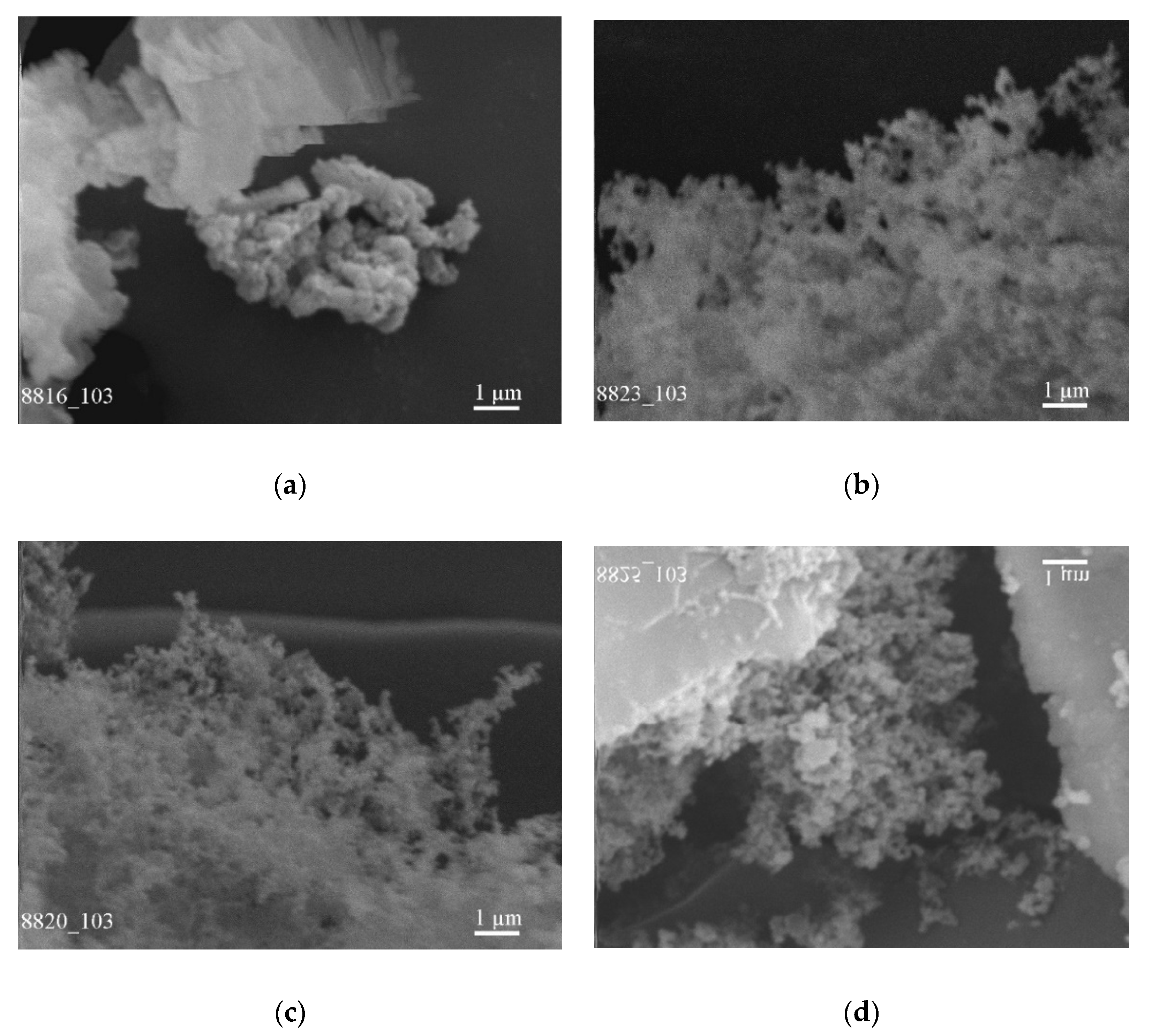
As an example, the effect of temperature distribution in the chamber while catalyst-free synthesis on the formation of the composite powder based on BN from the initial boron powder with a mean particle size of 0.20 μm was considered (Figure 6a–d), (Table 1). The plate-like particles of a thickness of 0.01 µm and a mean size of 7.00 µm were revealed on the upper central surface of the chamber (Figure 6a) (Figure 4b, location 4) and on the surface of water-cooled copper screens closer to the reaction zone (Figure 6d) (Figure 4b, location 2) as well as nanoparticles of the mean size of 0.35 µm and 0.15 µm, respectively. Nanoparticles of a mean particle size of 0.05 µm were formed on a left-side water-cooled flange (Figure 6b) (Figure 4b, location 1) and on the remote right-side water-cooled flange (Figure 6c) (Figure 4b, location 7). Such size distribution of the composite particles is due to the influence of the flow of nitrogen which captures light particles and carries them over long distances. The continuously ascending flow of boron nitride vapor from the boiling surface and its rapid cooling on the chamber surface results in the increased mean particle size of the composite powder that precipitates on the upper central surface of the chamber up to 0.35 μm (Figure 6a) (Figure 4b, location 4).
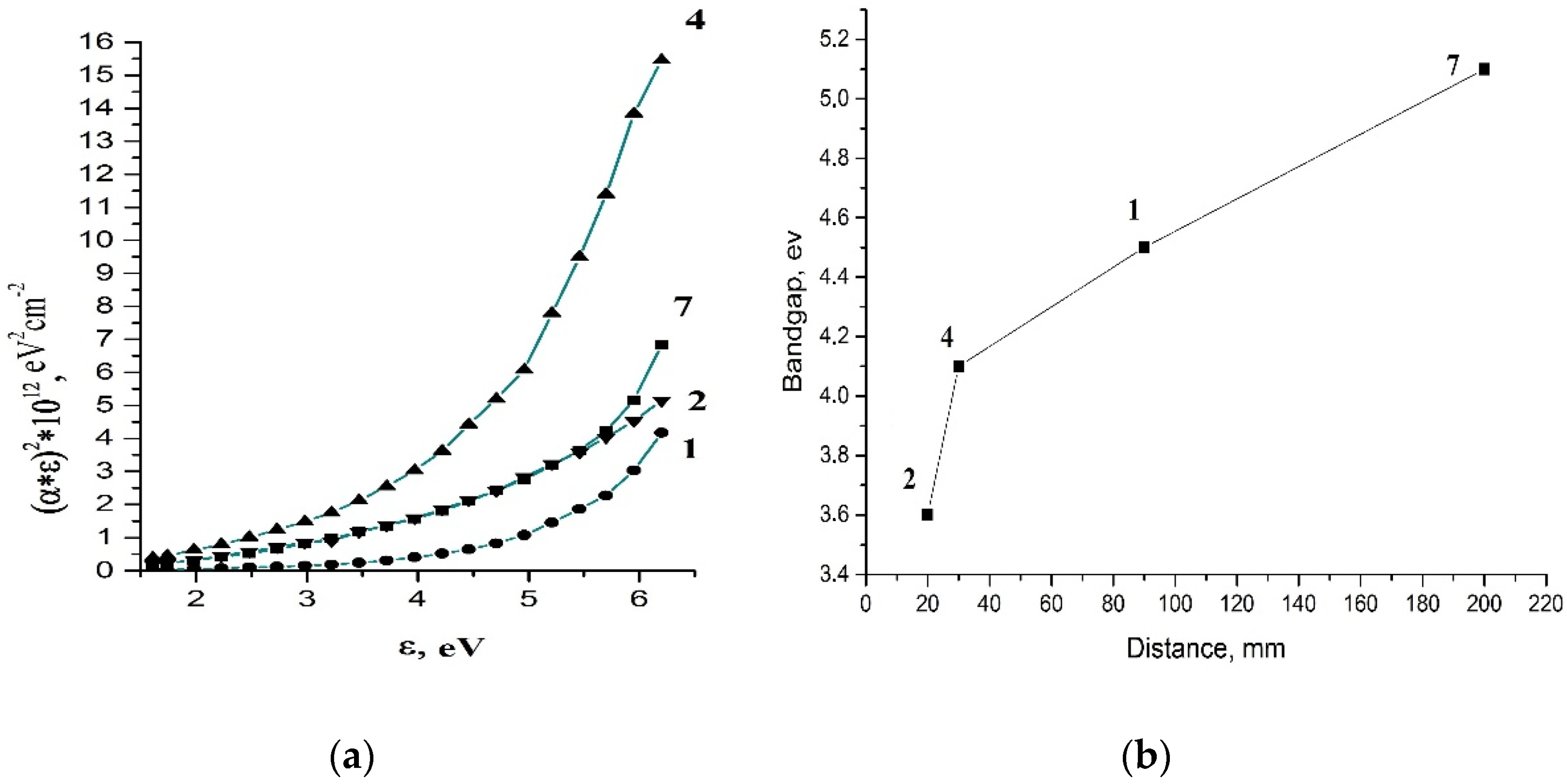
Optical absorption of the powdered material deposited in four parts of the chamber (Figure 4b, locations: 2, 4, 1, 7) was explored. All films of the powdered material deposited on a quartz substrate have demonstrated a high visible transparency. The representative graphs of a square optical absorption coefficient α versus photon energy at room temperature for various BN films are very different (Figure 7a). However, it is interesting to note that, regardless of the exact absorption coefficient values, there is a pronounced tendency for the bandgap to increase with the distance from the reaction zone. It can be concluded based on extrapolating the square optical absorption coefficient to zero (Figure 7a) that the highest bandgap is 5.2 eV for the material taken at the most remote part of a chamber (Figure 4b, location 7). The presence of linear sections in the graph of a square optical absorption coefficient α versus photon energy for powder material of a mean size of 0.35 μm collected on the upper central surface of the chamber (Figure 4b, location 4) indicates the availability of crystalline phases, that have time to form in the largest particles due to their rapid cooling on the chamber surface in a continuously ascending flow of boron nitride vapor from the boiling surface.
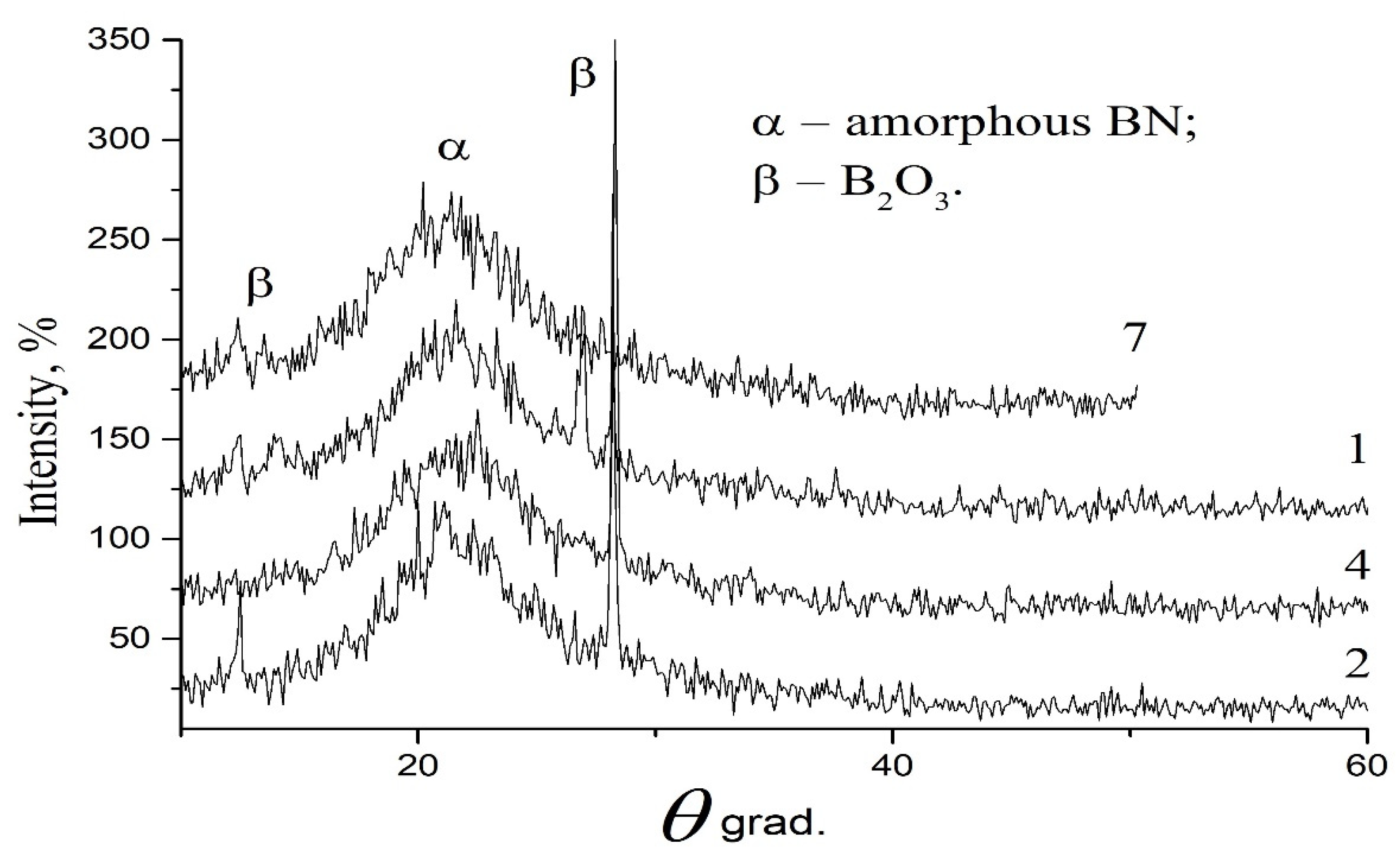
XRD data confirm and explain the pattern of change in the bandgap with the distance from the reaction zone (Figure 8). The appearance of B2O3 and B2O crystalline phases on the water-cooled copper screens of a chamber (Figure 4b, location 2) and on the surface of the quartz chamber (Figure 4b, location 4) near the reaction zone can explain the presence of oxides in the phase composition of the initial boron (Figure 2b), which are a constant supplier of oxygen when the initial boron is heated in a close proximity to the reaction zone (Figure 4b, location 2, 4). The presence of two linear sections in the graph of a square optical absorption coefficient α versus photon energy (Figure 7a, (graph 4)) is also attributed to the existence of additional oxides with a smaller bandgap. High temperature gradients and nitrogen flow result in deposition of a nanosized amorphous powder on the remote end of the chamber (Figure 4b, location 7), since the nanoparticles do not have enough time for complete crystallization and oxidation.
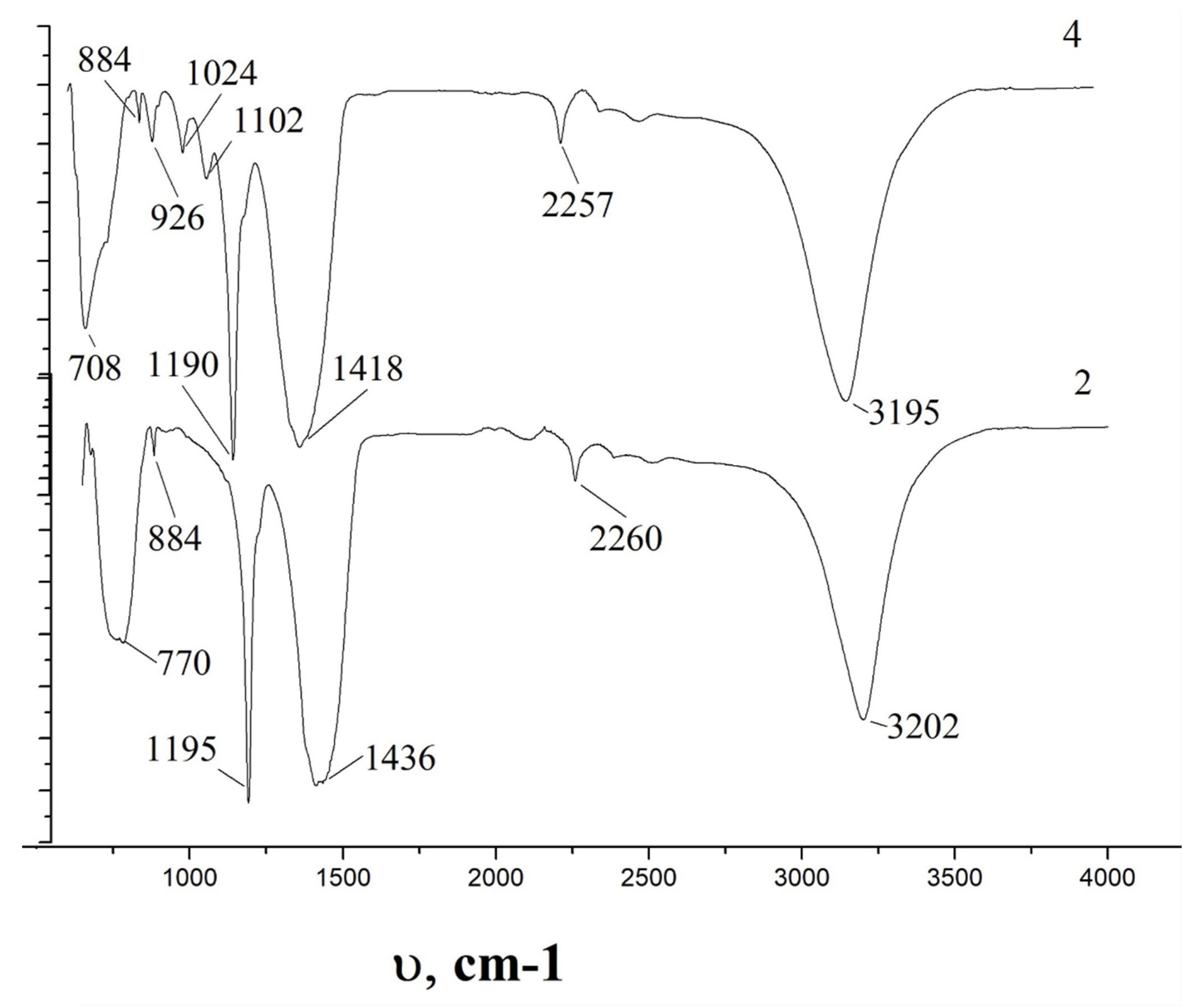
The vibrational IR spectra of the powder deposited on the water-cooled copper screens of the chamber (Figure 4b, location 2) and on the upper central surface of the chamber (Figure 4b, location 4) disclose the difference in the surface structure of these powders, caused by the action of the ascending flow of nitrogen and different temperature conditions, which are determined by the distance to the reaction zone (Figure 9). High temperatures near the reaction zone on the water-cooled copper screens of the chamber result in changes in phase composition on the particle surface since there is a disappearance of the bands at 926, 1024, 1102 cm−1, associated with the transitional phases of BN powder (Figure 4b, location 2). The main peaks at 708, 1190, 1418, 3195 cm−1 shift to higher values: 770, 1195, 1436, 3202 cm−1 (Figure 9, graf.2) at higher temperatures. Lower values of the bond lengths for the particles which were deposited on the upper central surface of the chamber (Figure 4b, location 4) may indicate a denser packing of the surface structure of these particles.
4. Conclusions
Joint heating of nitrogen and boron under concentrated light can ensure the formation of particles of different sizes and architecture depending on the synthesis conditions. The incorporation of the catalyst in the initial boron promotes the formation of mainly graphene-like structures and nanostructures of a mean particle size of 0.80 μm.
Under the effect of the flow of nitrogen and the decrease in temperature caused by increasing the distance to the reaction zone, the powders are separated by size and architecture. As a result, an amorphous powder with the largest bandgap of 5.2 eV with a minimum particle size of 0.05 μm and a minimum amount of oxide phase B2O3 precipitates in the most remote parts of the chamber.
Vibrational FTIR spectra of the deposited powder displayed that a close distance to the reaction zone and high temperatures ensure the disappearance of bands of 926, 1024, and 1102 cm−1, which is associated with the transitional phases of BN. A greater distance to the reaction zone and lower temperatures lead to lower values of the bond lengths for the particles which were deposited on the upper central surface of the chamber, and may indicate a denser packing of the surface structure of these particles.
Author Contributions
Conceptualization, writing—original draft preparation, writing—review and editing, L.S.; methodology, A.K.(Anatoliy Kasumov) and A.K.(Alexander Koval); investigation, L.S., A.K.(Anatoliy Kasumov) and A.K.(Alexander Koval); project administration, G.F. All authors have read and agreed to the published version of the manuscript.
Funding
This research received no external funding.
Institutional Review Board Statement
Not applicable.
Informed Consent Statement
Not applicable.
Data Availability Statement
Not applicable.
Acknowledgments
We acknowledge also support from Hirofumi Takikawa, Mototsugu Sakai, and Associate Hiroyuki Muto.
Conflicts of Interest
The authors declare no conflict of interest. The funders had no role in the design of the study; in the collection, analyses, or interpretation of data; in the writing of the manuscript, or in the decision to publish the results.
References
- Oku, T.; Hiraga, K.; Matsuda, T. Growth of Boron Nitride Nanohorn Structures. Mater. Trans. 2008, 49, 2461–2464. [Google Scholar] [CrossRef] [Green Version]
- Oku, T.; Kuno, M.; Kitahara, H.; Narita, I. Formation, atomic structures and properties of boron nitride and carbon nanocage fullerene materials. Int. J. Inorg. Mater. 2001, 3, 597–612. [Google Scholar] [CrossRef]
- Oku, T.; Hirano, T.; Kuno, M.; Kusunose, T.; Niihara, K.; Suganuma, K. Synthesis, atomic structures and properties of carbon and boron nitride fullerene materials. Mater. Sci. Eng. B 2000, 74, 206–217. [Google Scholar] [CrossRef]
- Kubota, Y.; Watanabe, K.; Tsuda, O.; Taniguchi, T. Deep Ultraviolet Light-Emitting Hexagonal Boron Nitride Synthesized at Atmospheric Pressure. Science 2007, 317, 932–934. [Google Scholar] [CrossRef] [PubMed] [Green Version]
- Dean, C.R.; Young, A.F.; Meric, I.; Lee, C.; Wang, L.; Sorgenfrei, S.; Watanabe, K.; Taniguchi, T.; Kim, P.; Shepard, K.L.; et al. Boron nitride substrates for high-quality graphene electronics. Nat. Nanotechnol. 2010, 5, 722–726. [Google Scholar] [CrossRef] [PubMed]
- Dang, H.; Liu, Y.; Xue, W.; Anderson, R.S.; Sewell, C.R.; Xue, S.; Crunkleton, D.W.; Shen, Y.; Wang, S. Phase transformations of nano-sized cubic boron nitride to white graphene and white graphite. Appl. Phys. Lett. 2014, 104, 093104. [Google Scholar] [CrossRef]
- Liu, L.; Feng, Y.P.; Shen, Z.X. Structural and electronic properties of h -BN. Phys. Rev. B 2003, 68, 104102. [Google Scholar] [CrossRef]
- Choi, H.C.; Bae, S.Y.; Jang, A.W.S.; Park, J.; Song, H.J.; Shin, H.-J. X-ray Absorption Near Edge Structure Study of BN Nanotubes and Nanothorns. J. Phys. Chem. B 2005, 109, 7007–7011. [Google Scholar] [CrossRef] [PubMed]
- Golovacheva, A.Y.; D’Yachkov, P.N. Effect of intrinsic defects on the electronic structure of BN nanotubes. J. Exp. Theor. Phys. Lett. 2005, 82, 737–741. [Google Scholar] [CrossRef]
- Chen, H.; Chen, Y.; Li, C.P.; Zhang, H.; Williams, J.; Liu, Y.; Liu, Z.; Ringer, S. Eu-doped Boron Nitride Nanotubes as a Nanometer-Sized Visible-Light Source. Adv. Mater. 2007, 19, 1845–1848. [Google Scholar] [CrossRef]
- Bernard, S.; Miele, P. Nanostructured and architectured boron nitride from boron, nitrogen and hydrogen-containing molecular and polymeric precursors. Mater. Today 2014, 17, 443–450. [Google Scholar] [CrossRef]
- Lipp, A.; Schwetz, K.A.; Hunold, K. Hexagonal boron nitride: Fabrication, properties and applications. J. Eur. Ceram. Soc. 1989, 5, 3–9. [Google Scholar] [CrossRef]
- Sartinska, L. Catalyst-free synthesis of nanotubes and whiskers in an optical furnace and a gaseous model for their formation and growth. Acta Mater. 2011, 59, 4395–4403. [Google Scholar] [CrossRef]
- Frolov, A.A.; Sartinska, L.L.; Koval’A, Y.; Danilenko, N.A. Application of the optical furnace for nanosized boron nitride production. Nanomaterials 2008, 2, 4. [Google Scholar]
- Sartinska, L.; Frolov, A.; Koval’, A.; Danilenko, N.; Timofeeva, I.; Rud’, B. Transformation of fine-grained graphite-like boron nitride induced by concentrated light energy. Mater. Chem. Phys. 2008, 109, 20–25. [Google Scholar] [CrossRef]
- Sartinska, L.L.; Eren, T.; Altay, E.; Frolov, G.A. Effect of moisture on the boron nitride formation from elements in a xenon high flux optical furnace. Eur. Chem. Bull. 2015, 4, 165–168. [Google Scholar]
- Sartinska, L. Surface modification to test “gaseous model” for BN nanotubes formation under the concentrated light and its application for graphene. Superlattices Microstruct. 2015, 85, 392–400. [Google Scholar] [CrossRef]
Figure 1.
SEM images of the initial boron powders of a mean sizes: (a)—0.05 μm; (b)—0.20 μm.

Figure 2.
XRD pattern of the initial boron powder of mean sizes: (a)—0.05 μm; (b)—0.20 μm.


Figure 3.
FTIR spectra of initial boron powders of mean sizes: (a)—0.05 μm; (b)—0.20 μm.

Figure 4.
A process chamber before heating with a sample inside (a) and its schematic sketch (b). Where: 1—a left-side water-cooled flange; 2—water-cooled copper screens; 3—a tablet of a compacted boron powder, which is placed in the center of the reaction zone, 4—a surface of a quartz chamber; 5—a copper tube for water supply; 6—copper tubes for input and output of nitrogen; 7—a right-side water-cooled flange. The resulting powder material was collected sequentially in 2, 3, 4, 1, and 7 locations in the chamber.

Figure 5.
SEM image of composite powder based on BN produced from initial boron powders of mean sizes: (a)—0.05 μm and (b)—0.20 μm. The powder material was collected from the surface of a compacted sample in a close proximity to the reaction zone (Figure 4b, location 3).
Figure 5.
SEM image of composite powder based on BN produced from initial boron powders of mean sizes: (a)—0.05 μm and (b)—0.20 μm. The powder material was collected from the surface of a compacted sample in a close proximity to the reaction zone (Figure 4b, location 3).

Figure 6.
SEM images of composite powder based on BN prepared using catalyst-free synthesis from initial boron powder of a mean size—0.20 μm. The powdered material was collected in 3 (a); 4 (b); 1 (c); and 7 (d) locations in the chamber (Figure 4b).
Figure 6.
SEM images of composite powder based on BN prepared using catalyst-free synthesis from initial boron powder of a mean size—0.20 μm. The powdered material was collected in 3 (a); 4 (b); 1 (c); and 7 (d) locations in the chamber (Figure 4b).

Figure 7.
Graphs: (a)—a square of the optical absorption coefficient α versus photon energy for the composite powder based on BN, collected in 2, 4, 1, and 7 locations of the chamber (Figure 4b) and (b)–bandgap versus the distance from the center of the reaction zone.
Figure 7.
Graphs: (a)—a square of the optical absorption coefficient α versus photon energy for the composite powder based on BN, collected in 2, 4, 1, and 7 locations of the chamber (Figure 4b) and (b)–bandgap versus the distance from the center of the reaction zone.

Figure 8.
X-ray diffraction pattern of the powder collected in 2, 4, 1, and 7 locations of the chamber (Figure 4b).
Figure 8.
X-ray diffraction pattern of the powder collected in 2, 4, 1, and 7 locations of the chamber (Figure 4b).

Figure 9.
FTIR spectra of the powder collected in 2 and 4 locations in the chamber (Figure 4b).
Figure 9.
FTIR spectra of the powder collected in 2 and 4 locations in the chamber (Figure 4b).


Table 1.
Formation of composite powders based on BN within the chamber.
| Locations of the Collecting Powders | Water-Cooled Copper Screens (Figure 4b, Location 2) | Upper Central Surface of the Chamber (Figure 4b, Location 4) | Left-Side Water-Cooled Flange (Figure 4b, Location 1) | Right-Side Water-Cooled Flange (Figure 4b, Location 7) |
|---|---|---|---|---|
| Distance from the reaction zone, mm | 20 | 30 | 90 | 210 |
| Mean plate-like particle size, µm | 7 | 7 | - | - |
| Mean nanoparticle size, µm | 0.15 | 0.35 | 0.05 | 0.05 |
Publisher’s Note: MDPI stays neutral with regard to jurisdictional claims in published maps and institutional affiliations. |
© 2022 by the authors. Licensee MDPI, Basel, Switzerland. This article is an open access article distributed under the terms and conditions of the Creative Commons Attribution (CC BY) license (https://creativecommons.org/licenses/by/4.0/).
Share and Cite
MDPI and ACS Style
Sartinska, L.; Kasumov, A.; Koval, A.; Frolov, G. Properties of Composite Powder Based on Boron Nitride Prepared under Concentrated Light. Condens. Matter 2022, 7, 42. https://0-doi-org.brum.beds.ac.uk/10.3390/condmat7020042
AMA Style
Sartinska L, Kasumov A, Koval A, Frolov G. Properties of Composite Powder Based on Boron Nitride Prepared under Concentrated Light. Condensed Matter. 2022; 7(2):42. https://0-doi-org.brum.beds.ac.uk/10.3390/condmat7020042
Chicago/Turabian StyleSartinska, Lina, Anatoliy Kasumov, Alexander Koval, and Gennadiy Frolov. 2022. "Properties of Composite Powder Based on Boron Nitride Prepared under Concentrated Light" Condensed Matter 7, no. 2: 42. https://0-doi-org.brum.beds.ac.uk/10.3390/condmat7020042