
The Cost of a True Random Bit—On the Electronic Cost Gain of ASIC Time-Domain-Based TRNGs


Faculty of Engineering, Bar-Ilan University (BIU), Ramat-Gan 5290002, Israel
*
Author to whom correspondence should be addressed.
†
These authors contributed equally to this work.
Cryptography 2021, 5(3), 25; https://0-doi-org.brum.beds.ac.uk/10.3390/cryptography5030025
Submission received: 5 August 2021
/
Revised: 11 September 2021
/
Accepted: 16 September 2021
/
Published: 18 September 2021
(This article belongs to the Special Issue Implementation and Verification of Secure Hardware against Physical Attacks)
Abstract
:Random number generators are of paramount importance in numerous fields. Under certain well-defined adversarial settings, True Random Number Generators (TRNGs) are more secure than their computational (pseudo) random number generator counterparts. TRNGs are also known to be more efficiently implemented on hardware platforms where, for various applications, efficiency in terms of electronic cost factors is critical. In this manuscript, we first provide an evaluation of robustness and reliability of efficient time-domain-based TRNG implementation over FPGA platform. In particular, we demonstrate sensitivities which imply a TRNG construction which is not agnostic to electronic-design-automation tools and to the level of designers’ know-how. This entails a large amount of effort and validation to make the designs robust, as well as requires a high degree of complexity from non-trivial FPGAs flows. This motivates the second part of the manuscript, where we propose an ASIC-based implementation of the TRNG, along with the optimization steps to enhance its characteristics. The optimized design improves the randomness-throughput by 42× for the same entropy level described in previous works, and it can provide maximal entropy level of 0.985 with 7× improvement in randomness throughput over the raw samples (no pre-processing). The proposed design simultaneously provides a reduced energy of 0.1 (mW/bit) for the same entropy level as previous works, and 1.06 (mW/bit) for the higher entropy flavor, and a lower area utilization of 0.000252 (mm) on a 65 nm technology evaluation, situating it in the top-class of the discuss ratings. This leads to the quantitative question of the gain in electronic cost factors over ASIC TRNGs, and the minimum Cost Per Bit/Source possible to date. Finally, we exemplify a TRNG versus PRNG cost-extrapolation for security architects and designers, targeting an ASIC scenario feeding a lightweight encryption core.
1. Introduction
Random number generators have various applications in statistics, probabilistic algorithms, simulations, cryptography, and other fields where producing an unpredictable result is desired. There are two main groups of random number generators: True Random Number Generators (TRNGs) which extract randomness from physical noise, and Pseudo Random Number Generators (PRNGs) which appear statistically random but are predictable. Two of the most widely used families of PRNG algorithms are Linear Feedback Shift Registers (LFSR), such as in References [1,2], and encryption in some mode-of-operation, e.g., the Advanced Encryption Standard in Counter mode (AES-CTR DRBG). These types of RNGs require an initial vector (seed) as a starting condition. The seed must be truly random, so that PRNG may include a seeding TRNG module, as well. A TRNG is a device that relies on a random physical process and extracts random numbers from it. These devices are often based on properties, such as thermal noise, the photoelectric effect, and other quantum phenomena. Theoretically, the physical phenomenon from which the TRNGs extracts randomness is completely unpredictable. Due to the growing importance of the generation of random numbers, several standards have been published. These standards specify the goals, tests, and criteria that the entropy sources must meet. The two main standards are SP 800-90B/C, the special publication of the National Institute of Standards and Technology (NIST), and the German BSI standard called AIS-31.
TRNGs are divided into two main classes based on the mechanism from which the noise is extracted. The first group is composed of metastable-based TRNGs [3,4,5,6,7,8,9]. This group forces an electronic topology to be in a metastable state and then releases it. The random noise in the system affects the outcome, which stabilizes on a (typically) binary value according to the noise, eventually producing a random bit stream. The second popular group of TRNGs extracts randomness from noise in the time domain [10,11,12,13,14,15,16]. In this study, we focus on low electronic-cost implementations of TRNGs. TRNGs can be implemented either within a software or a hardware platform in cases where hardware randomization is required. Hardware implementations are generally more efficient owing to the fact that they generally make use of noisier physical phenomena to extract randomness. Our primary goal is to advance the efficiency of existing state-of-the-art hardware constructions which have mainly been evaluated over Field Programmable Gate Arrays (FPGAs) and to evaluate the efficiency of the improved version on Application Specific Integrated Circuit (ASIC) technology.
The main criteria for TRNG implementations are electronic cost-related, e.g., how much a random-bit generation costs in energy consumption, area utilization, and what randomness-throughput can be achieved. Clearly, the underlying assumption is that we will only compare TRNG flavors which provide a sufficient level of entropy.
The time-domain-based architecture of the ES-TRNG proposed at CHES-2018 by Yang et al. [17] uses a slow ring oscillator (RO) to sample a fast RO. Due to randomly distributed noise in the system, jitter is accumulated on the fast RO, which, in turn, causes a random phase shift. This randomness in the jitter is translated into a randomly sampled bit value. Two novel techniques were used in the implementation of ES-TRNG, namely variable-precision phase encoding and repetitive sampling. These two techniques improve the randomness-throughput and decrease the area utilization and energy consumption of the circuit, while maintaining high min-entropy. In this study, we implement these efficient ES-TRNG designs on different platforms (FPGA, ASIC) and demonstrate the design challenges on FPGAs. We exemplify and discuss the extent to which the design on an FPGA is sensitive to the implementation location, automatic FPGA routing, the LUT structure implementation choices, and various other features, making it challenging to construct it robustly on FPGAs.
This analysis leads to the main thrust of this work, namely improvements to the baseline ES-TRNG on an ASIC platform. These are expected to improve FPGA due to the inherent performance gains of ASICs. We show how to significantly improve on all criteria by exploiting the design flexibility of ASICs, removing the complexity of custom design steps on FPGAs, using ASICs’ easy design flow, and the controlled and deterministic nature of flow steps, such as routing. We then discuss optimizing specific circuitry mechanisms within the ES-TRNG to improve its efficiency. Our goal was to respond to the question of the minimal (electronic) cost of a truly random bit/source on efficient ASICs. These quantities can translate directly into higher level, e.g., cryptographic design choices and the selection of primitives.
Here, we innovate by developing a concrete optimization and guidelines for design on ASIC relating to various topological, circuit, and architectural features, which together yield significant improvements. We compare all designs prior to pre-processing on the raw generated bits for fairness, as shown in Table 1. For example, the optimized design improves in randomness-throughput by 42× for the same entropy level described in previous works, and it can even provide a considerably improved entropy level of 0.985 with 7× improvement in randomness throughput. The proposed design simultaneously enables a reduced energy of 0.1 (mW/bit) for the same entropy level as previous works, and 1.06 (mW/bit) for the higher entropy flavor, and a lower area utilization of 0.000252 (mm) on a 65 nm technology (widely utilized for low-cost IoTs, RFID devices, etc.). Our optimization efforts and proposed implementation is compared in details to several other ASIC-based TRNGs [7,18,19,20,21,22,23,24,25,26,27,28,29,30,31,32], both ring-oscillator- and non-ring oscillator-based, in Section 5. The proposed TRNG is the smallest known to date, to the best of our knowledge, considering [26] (see Table 1) and provides the best-in-class , as summarized in Section 5.
1.1. Contributions
The main contributions of this study are as follows:
- Providing an evaluation of the robustness and reliability issues of efficient TRNGs implemented over FPGA platforms. In particular, we demonstrate its sensitivity to physical properties, such as routing, and device placement, in terms of the amount of effort required to make a design robust, and the degree of complexity of non-standard FPGAs flows.
- Proposing an ASIC-based implementation of the TRNG, along with the optimization steps, to enhance its characteristics that lead to significant performance-entropy improvement.
- Discussing the quantitative question of how much gain in electronic cost factors can be expected over ASIC TRNGs, and the cost Per Bit/Source. To facilitate easy extrapolation for security architects and designers, we exemplify a TRNG versus PRNG ASIC test-case feeding a lightweight encryption core.
Paper Organization and Roadmap
First, in Section 2, we briefly detail min-entropy estimation, and TRNG related criteria, such as randomness-throughput and area per source. In Section 2.2, we describe the time-domain efficient TRNG which was used as a baseline gold standard and comparison point. In Section 3, we provide a detailed discussion of the implementation space over an FPGA platform and supply measurement results pinpointing platform-dependent sensitivity as a function of the design parameters of the TRNG. We then present a detailed description of ASIC construction, while analyzing the design intent, parameter optimization and limitations to provide a best-in-class ASIC TRNG in Section 4. Next, we make a detailed comparison through a wide-reaching state-of-the-art survey and analyze examples of gains utilizing the proposed TRNG as compared to a PRNG in Section 5. We conclude the manuscript in Section 6.
2. Tools and Theory
In this subsection, we discuss the (standard) tools we used to evaluate min-entropy. We further detail the evaluation of other criteria, such as randomness-throughput, area, and energy per bit (source). In addition, we also review the basic properties of the time-domain-based TRNG we utilized as a baseline gold standard comparison point, i.e., the ES-TRNG.
2.1. Entropy Evaluation and Efficiency Criteria
Whereas the entropy of a sequence is well-defined when it is possible to exhaust/ enumerate the full distribution space, the entropy of a finite sample (partly observable) is quite hard to evaluate. Nevertheless, there are advantages to providing a measure of the quality of the randomness sources. In 1948, Shannon defined the entropy of a sequence i with n possible options as:
In the binary, single bit case: . With uniformly distributed random bits, we reach the maximum entropy of 1.
However, as described above, a TRNG sequence is a random process which provides infinite length sequences, or exhibits complex stochastic behavior and has a potential dependency between bits (even if these are claimed to be independent by the model). For this reason, there has been extensive research on the question of estimating the minimum-entropy of a sequence which has aimed at bounding the worst case. For this purpose, several entities, such as the National Institute of Standards and Technology (NIST) and the Bundesamt für Sicherheit in der Informationstechnik (BSI), have defined a variety of statistical tests that complement and cross-verify each other to estimate the min-entropy level. Roughly, two main types of tests are performed: the restart test and the sequential test.
The restart test investigates in/dependencies between sequences when the generator ‘wakes up’ or is restarted, or, alternatively, if it takes time to enable proper operation. In this test, 1000 sequences of 1000 bits are produced and gathered into a matrix of size 1000 × 1000, which is tested for various properties, such as periodicity, patterns and repetitions, correlations between rows, etc., and it outputs a minimum-entropy estimation. The second class is the sequential test which is designed to ignore the non-stable entropy value at the beginning of the sequence. It is aimed at quantifying the minimum entropy in steady state. To provoke it, a sequence of 1,000,000 bits is collected and checked for entropy for subsets of different numbers of bits. The claim is that a combination of the evaluation of the two tests with a valid stochastic model will give a good indication of the TRNG min-entropy level. The stochastic model provided by the designer should comply, to some extent, with the results from the tests, as stipulated in the BSI criteria.
We evaluated the efficiency of a generator by its Randomness-Throughput (RT) and Area utilization/Energy consumption per bit (or source): The randomness-throughput (RT) is defined by . For the specific case of the ES-TRNG-based construction, it can be approximated by (Mbit/s), where is the accumulation time required to wait until enough time-domain jitter noise has accumulated (elaborated below). The energy (average power) per bit or source is defined as the average energy (average power) required to produce one random bit.
2.2. Time-Domain Efficient TRNG
As discussed above, our informal goal was to explore the minimum electronic cost to generate random bits. In previous works, the ES-TRNG demonstrated exquisite properties, supported by a stochastic model, as shown in a thorough evaluation over FPGAs, etc. Therefore, it was chosen as the gold standard for implementation. To the best of our knowledge, however, it does not provide a reference to the maximum known efficiency (as discussed and illustrated in Table 3).
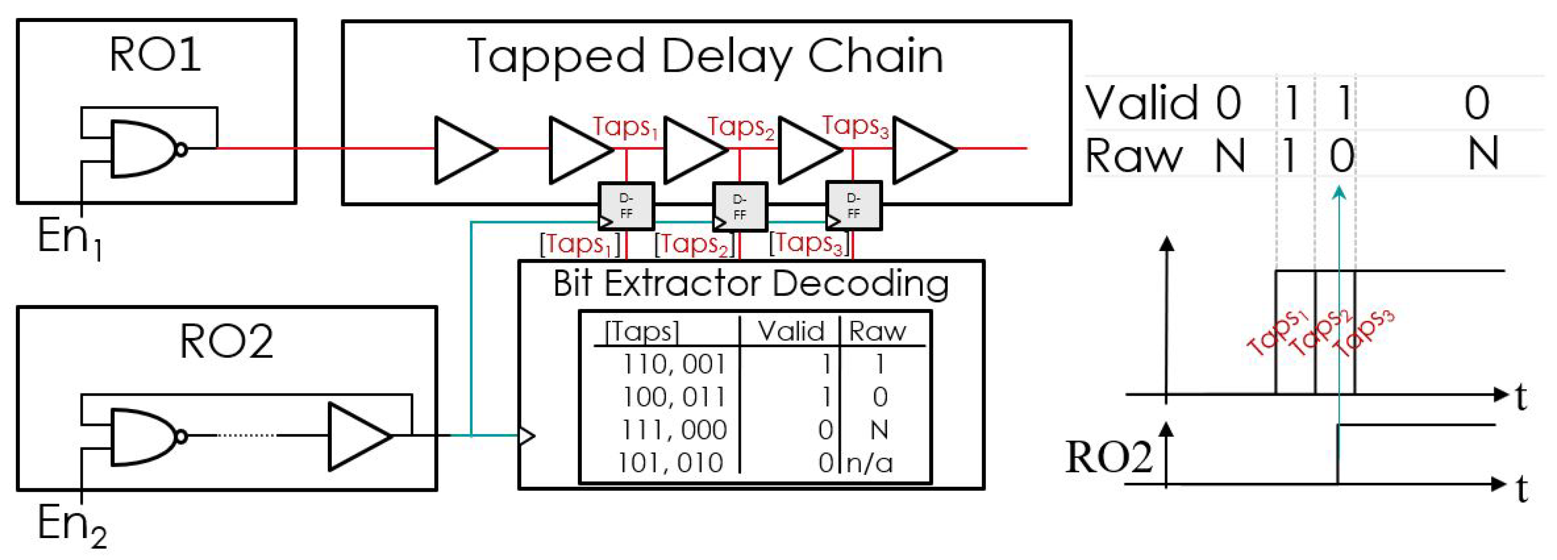
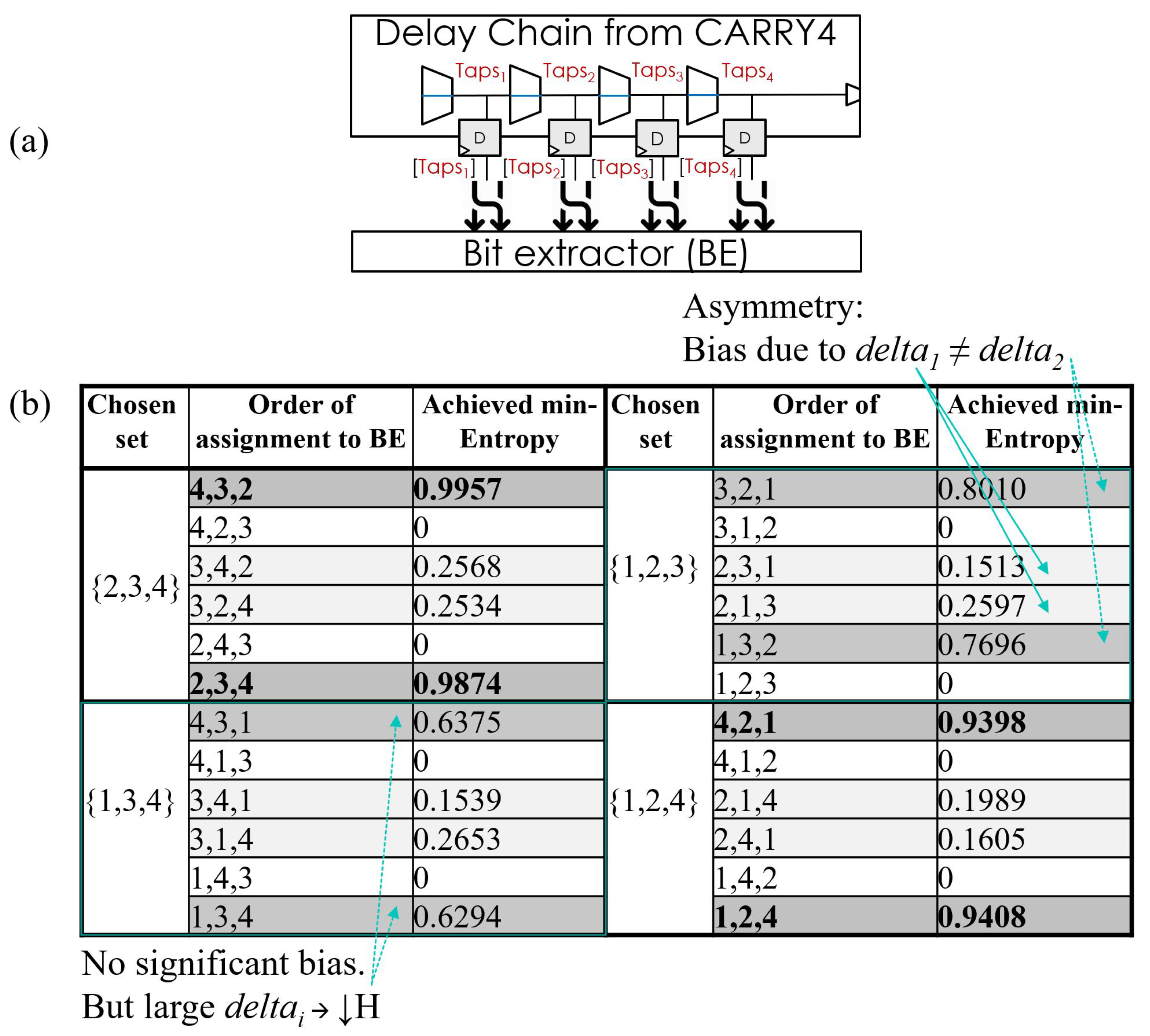
Similar to the vast literature on time-domain TRNGs, the ES-TRNG architecture is based on extracting entropy from jittery signals (over time). The source of randomness is a free-running ring oscillator. The design goals of the ES-TRNG are to achieve an area compact implementation and to provide a reasonably high randomness throughput, while also incurring low engineering effort. The architecture is based on high-precision edge sampling of the jittery signal (i.e., time resolution). Two techniques are used to improve the throughput and reduce the resource utilization. The first technique is variable-precision phase encoding, which utilizes a selective high-precision sampling process. It provides a compact implementation which only needs a short jitter-noise accumulation time to reach a sufficient entropy level. The output of the free-running oscillator (RO1) passes through several delay elements constructed by a tapped delay chain element inside an FPGA slice. These delays aim to provide a much smaller delay than the period of RO1. The digitization module, as illustrated in Figure 1, captures the oscillator phase with high precision around the signal edges. This region is called the high precision region. The samples of this region are encoded into values of 1 or 0, depending on the phase. The remainder of the time samples, i.e., time samples that are farther away from the rising/falling edge, are denoted by low-precision samples, and this region is encoded as Null (N). The sampling of the delay chain is triggered by a rising edge of another slower ring oscillator, RO2. The second technique is repetitive sampling, which allows for multiple sampling in one system clock cycle by utilizing the RO2 oscillator which is faster than the system clock. This technique enables a high-throughput TRNG.
As shown in Figure 1, the bit-extractor implements the desired logic to decode the phase status of RO1 relative to RO2’s rising-edge (i.e., high-precision and its 1 or 0 raw value, or low precision). It does so by capturing the sampled versions of the tapped-delay chain outputs, Taps(2:0). The sampled signals are denoted by (Taps(2:0)) as the output of three Flip-Flops (FFs). The bit extractor provides the raw bit, along with a alidity signal, as outputs.
3. On the Variability of FPGA-Based Implementation
Generally, owing to its reconfigurability properties, FPGAs have been adopted widely and have recently breached the market barrier of high performance servers and artificial intelligence. They are also being embedded in custom ASIC flows, e.g., eFPGA, and are driving increasingly more new markets and applications. Clearly, FPGAs have a faster design cycle for standard digital applications. However, FPGAs are designed to provide efficiency for a wide variety of benchmarks which are representative of certain application domains. Hence, to some extent, they are hard to tailor to non-standard use cases, especially if the performance criteria of the design do not correspond to standard digital criteria. Examples include the utilization of FPGAs to build analog in-nature primitives, such as TRNGs. Their objective criteria, e.g., the min-entropy, which depends on characteristics that are not optimized by-design with FPGA flows, are much harder to control than in the case of ASIC flows. In turn, for circuits, such as TRNGs, inherent losses in performance and accuracy/certainty are likely to persist as a result of FPGA-abstraction.
In this section, we describe the implementation of the ES-TRNG module on an FPGA device. We begin by describing the resources for efficient area-utilization implementation and then turn to issues of robustness and variability. Our main goal here is to show that quite complex design steps are required from an FPGA design-flow perspective to make the design robust. Specifically, the controlled placement and routing on FPGAs are hard and are specific to the individual FPGA environment/vendor. Often, not all design details are available to the designer, which impinges on design certainty. This is a challenge for highly sensitive TRNG constructions. In the following, we provide a detailed analysis and explanations of our attempts to control the physical parameters, oscillator periods, and deterministic nature of the hardware elements or location independence, all of which translate directly into the hurdles of reduced performance and design margins.
This section provides the underlying rationale governing the enhancement of all these features within an ASIC implementation flow, as well as the opportunities to achieve further significant optimizations with respect to the determinism and set of tools available within an ASIC design-flow. We detail all these issues in the next section.
3.1. Circuit Level Implementation
We implemented the design over a Xilinx Spartan-VI FPGA device (45 nm technology node), since it is one of the most commonly used FPGAs tested in previous publications on TRNGs. Therefore, this selection is opportune from a comparative point of view but also because this technology is more relevant to the type of (rather) low-cost devices which will require these TRNGs, such as RFIDs, sensors, and IOTs, in general. To communicate with the underlying TRNG, a standard communication protocol interface was implemented on the FPGA fabric.
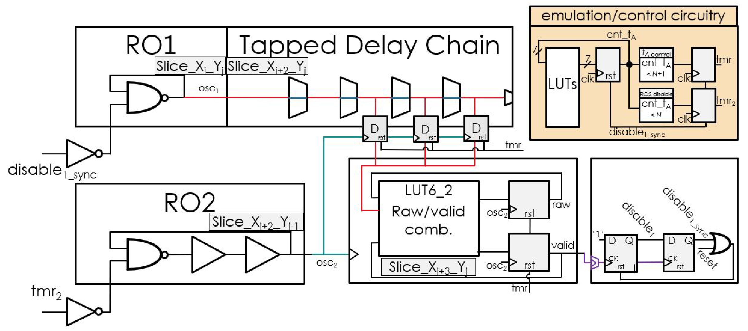
The baseline resources utilized to construct the TRNG are illustrated in Figure 2. The (RO1 signal) was implemented using one 5-input Look-Up-Table (LUT5) of the A type, ALUT, which functions as an NAND2 element. It was located in an anchor slice with coordinates on the FPGA. All the other components were located in slices relative to it. The tapped delay chain used to provide the delayed replicas of osc1 was constructed as a dedicated carry propagation chain CARRY4 with three taps, , , and . These three taps were sampled by three consecutive flip-flops in the same slice. These flip-flops were asynchronously reset low by the signal and (RO2 signal) as the clock input. was implemented using three LUT5 elements (an NAND2 and two buffers, BUF), placed in the same FPGA slice and in relative locations to . The sampled signals were directed to one LUT6_2 instance to generate the and signals. The signals were stored in two available flip-flops (all in the relative slice ) and asynchronously reset low by the signal and as their clock input. The sampled versions of the and signals were fed back to the same LUT6_2 to help compute the next and . After being sampled, the signal passed directly to an edge-detection and synchronization module. The edge-detection and synchronization module detected when the signal was in logic 1. The valid signal was used as a clock for the first flip-flop and logic 1 as input. This flip-flop generated the output signal . In order to synchronize, the output of the first flip-flop was sampled by a second flip-flop which was triggered by the system clock as its clock input. It generated a synchronized signal denoted . This signal and the system were ORed to reset the edge-detection after more than 1 system clock cycles.
The validation/ testing circuitry implemented a jitter accumulation cycle counter circuitry which was constructed with a 7-bit counter asynchronously reset by the signal to generate the cnt_ signal. The counter value was continuously monitored. When it was smaller than a defined value (say, N + 1), the signal was generated; this signal reset the high-resolution edge sampling mechanism and the / circuitry. Another comparator, set to the value of N, was implemented to trigger another signal, . This signal was used to reset . Basically, the combination of and controlled the time with the resolution of a system clock cycle. The area resources needed to implement this feedback loop consisted of four LUT6_2 elements and nine flip-flops, which was considerable, as compared to the rest of the design. This cost can be reduced if a smaller control resolution is required or a specific value is known in advance. However, it is important to emphasize that this circuitry was only needed for testing and calibration, etc., and only a small part of it was actually needed. Typically, a designer knows the values needed in advance and defines a safe margin.
3.2. Platform Dependent Sensitivities
In the following, we detail the implementation-independent design sensitivities. Inherently, owing to unknown IP parameters provided by FPGAs, a (naive) designer may provoke a non-ideal scenario which impedes the expected design outcomes. Ideally, it would be nice to produce a design which is not agnostic to designer choices, as long as the design follows the functional intent. However, in real life, owing to implementation platform unknowns, each and every design choice can be crucial. They reflect the set of critical aspects which need to be evaluated when implementing a very noise-sensitive structure and a topology-sensitive structure, such as a TRNG.
We first describe several design parameters which are hard to set/verify and not well supported by native FPGA design flows. This is natural since these parameters are an outcome of a security-in-mind requirement and not a traditional digital design requirement. They lead to designer choices which are not easy to evaluate or verify. As a result, as shown below, they affect highly important parameters, such as the min-entropy levels.
3.2.1. Oscillator Ratio ()
One of the most important parameters in an ES-TRNG design is the ratio between the periods of the two oscillators (RO1, driven by ; and RO2, driven by ). The ratio mainly affects duration, since jitter accumulates within the oscillator RO1 until it is sampled by RO2, denoted . If the ratio is well-defined (e.g., see discussion on the 4/5 ratio in Reference [17]), the probability of sampling within the high-resolution state (valid bits) is high, and the number of needed repeated samples is low. Both contribute to shorter . Deviations from good ratios can have a significant effect, as we discuss below. We follow by discussing and exemplifying the high design-variability per FPGA design-flow step.
Elaboration and placement: It is challenging to design a ring-oscillator and set its period with high certainty using standard FPGA design tools. This is because standard timing notations and timing simulators use abstraction (i.e., by default some variability is permitted), so that the tools can set an upper and lower bound on the timing characteristics of the clock signals. However, they do not provide a mechanism to set them definitively. Moreover, FPGAs are composed of small building blocks which are used to construct programmable logic elements; in turn, there are numerous options to implement an inverter or a buffer within a LUT, for example. For dedicated tailored blocks, such as TRNGs, we typically specify the exact way to implement an RO buffer in a LUT by design, i.e., which LUT input and output to use and how to set the other constant LUT inputs. Each one of the implementations induces a different noise sensitivity, which is typically poorly simulated over FPGA platforms (with high variability) and different timing behaviors. As discussed above, since timing information tends to exhibit variability in FPGAs reporting timing tools (relatively large margins), small deviations from the required timing exist, though the reported design intent is met, i.e., the timing is bounded. This is crucial since we are interested in maximum performance TRNGs (high throughput). Further, small deviations in the ratio of oscillators, which is even more sensitive to small absolute errors, can significantly affect the min-entropy of a generator. This challenge translates into a very complex design cycle, where it is not only hard to set certain periods with certainty, but these must also be verified over many instances before we can certify the generator. There are a number of mechanisms to remedy this situation, all of which induce more uncertainty: because ring oscillators, such as the ones needed here, work at a very high frequency (the maximum possible on FPGAs) to increase throughput, they cannot be measured directly, for example, by an oscilloscope or characterized. Rather, we first need to either divide the frequency in hardware and only then approximate (bound) the achieved frequency internally, add logic internally, such as counters, for the same purpose or alternatively, approximate delays by taking long chains that produce slow and measurable signals, and attempt to extrapolate the period. None of these methods are straightforward and will, in any case, induce variability between the desired and implemented periods.
Routing: The aforementioned challenge is more closely related to the designer’s by-design choices. However, there is a more formidable challenge with (simple) FPGA design flows. After the logic synthesis, and element mapping to the FPGA’s logic resources and placement, a routing phase takes place. The routing phase is extremely complex and routing information, such as delays, is highly elusive from a designer’s perspective since delay libraries and characterizations are much less easily available than information relating to logic elements. Moreover, whereas logic elements can be easily set with determinism within standard design flows and constraints, controlling routing and reasoning the outcome of some constraints is much harder. There are several design flows known as Hard—(FPGA)—Macros, which allow for the specific selection of routing and constraining, or duplicating them if needed. However, such design steps are typically much more complex, less portable, and require more expertise. Nevertheless, reasoning the impact of a design change with routing layers is still a significant hurdle, especially when the optimization criteria (i.e., the period-ratio, noise effect, cross-talk, and the outcome min-entropy) are not part of the traditional digital-design metric specified for the tools.
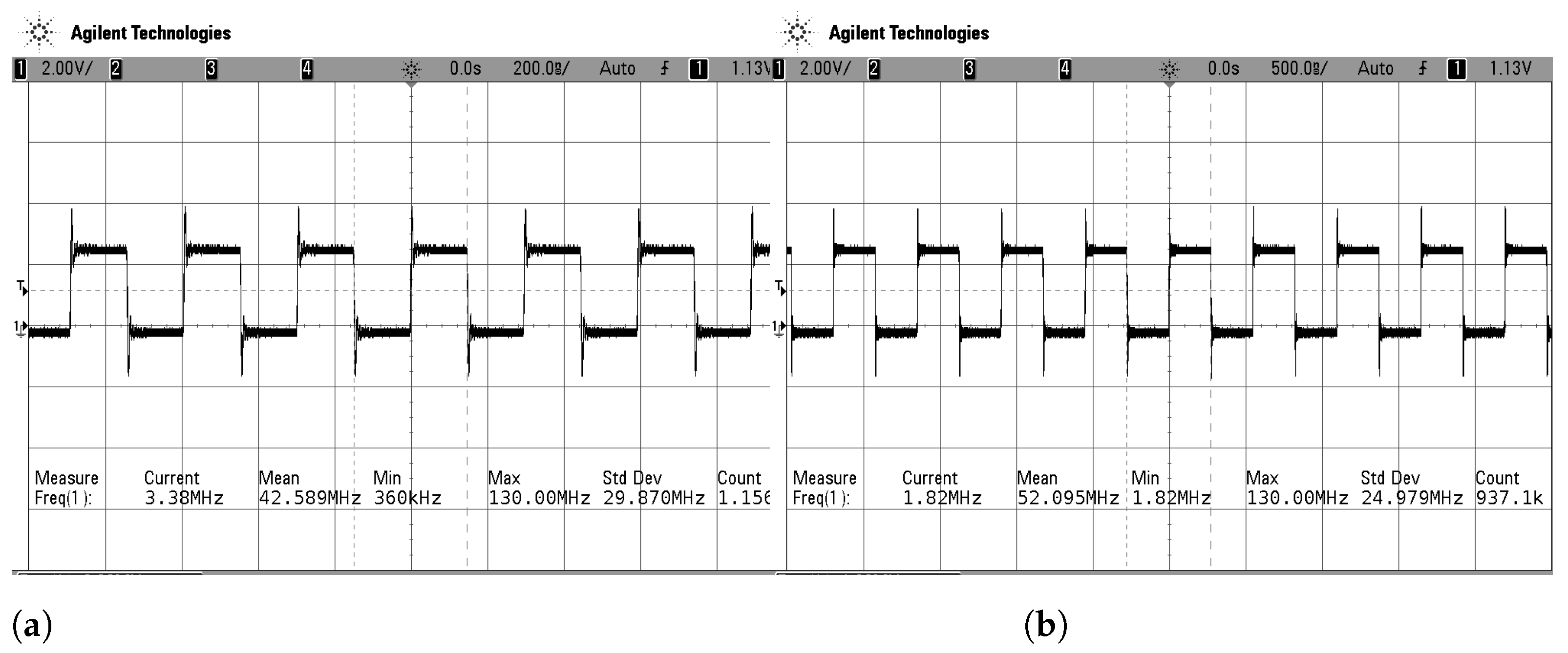
To design a robust ES-TRNG, we followed the well-defined guidelines in Reference [17] for oscillator periods. However, some design parameters, which were probably well set, were not mentioned by the authors. For example, constraints, such as the exact FPGA-slice locations, the distance of specific elements within the logic, the specific {LUTs, FFs} chosen, and how the constants were set to LUTs inputs, can all significantly affect the outcome. After carefully tailoring all the aforementioned parameters, we initiated a design stage to evaluate our RO periods. This consisted of (1) a standard post place and route timing simulation after careful timing constraints were applied on the RO periods; (2) implementing fast clock-dividers on the hardware and outputting the slow-signals on the IOs to an oscilloscope; and (3) constructing repetitive delay elements chains with varying length, measuring the induced delay on these long paths, and extrapolating and averaging to capture the period of a subset of elements.
All these methods produced different simulated/measured/extrapolated values. The maximum deviation of a clock period between all methods was 15%; however, the maximum deviation of the clocks-ratio was 30%, which is considerable. The design method we found to be the most robust was to utilize the clock dividers and actually measure the outcome frequency. This is because, internally, an oscillator sees an output load of a register very close to it, which is very similar to the type of load it will experience once the actual design is mapped. Moreover, timing constraints did not allow us to verify whether the oscillating signal was being correctly sampled and divided. Finally, we actually visualized the outcome signal. However, the disadvantage is that using this type of divider chain in our very fast-signal case required 4 clock dividers, as well as accumulated 4 stages of error on the estimation of the period. The evaluated average measured frequency of one LUT; one inverter feedback ring oscillator was 603.16 MHz, after multiplying by 16 (4 dividers). To verify this result we constructed variable length repeated chains of odd numbers of LUT-inverters and repeated the experiment. Figure 3a,b illustrates two examples of 11 elements and 21 elements showing the average computed frequencies of 3.38 MHz and 1.82 MHz, respectively, corresponding to internal frequencies of ∼54 MHz and 20.1 MHz (multiplied by ).
As discussed in Reference [17], the oscillator ratio was set to 0.79 which is close to the theoretical 4/5 ratio which was expected to provide nice properties according to the stochastic model. With this in mind, we tested for the best configuration to achieve a 4/5 ratio. We evaluated 3 different designs of oscillators with {4, 5}-elements for {RO1, RO2}, respectively. However, to deal with the uncertainty factor, as discussed above, we also evaluated {3, 4}-elements and {5, 6}-elements tuples for {RO1, RO2}, respectively. In theory, we expected the 4/5 design to provide the best results. However, as was detailed above, with an uncertainly of, at most, 30% in the ratio, as derived from experiments, we predicted we would fall short of our design intent. Indeed, the results of the 4/5 and the 3/4 design failed to pass the NIST min-entropy tests; the 5/6 design was the only one to pass the tests given the expected entropy level analyzed by the stochastic model. This outcome alone forced us to reduce the oscillator frequency (more devices), further reducing the randomness-throughput of the generator.
In yet another attempt to achieve maximum performance, we explored a {1, 3}-elements tuple for {RO1, RO2}, respectively, by manipulating the topology and structural characteristics of the ROs to achieve a close enough ratio to 4/5. First, we examined which LUT to use at a specific FPGA-slice and the selected LUT within a slice. These choices inflict significant changes, even if routing is deterministic. Moreover, they introduce different variability factors, making the design less stable in terms of min-entropy. We have situated RO1 in every possible LUT in a specific slice for a set RO2 oscillator. We exhaustively executed the same steps for RO2, which is composed of 3 LUTs (! options for 3 out of the possible Spartan-VI {A, B, C, D}-LUTs).
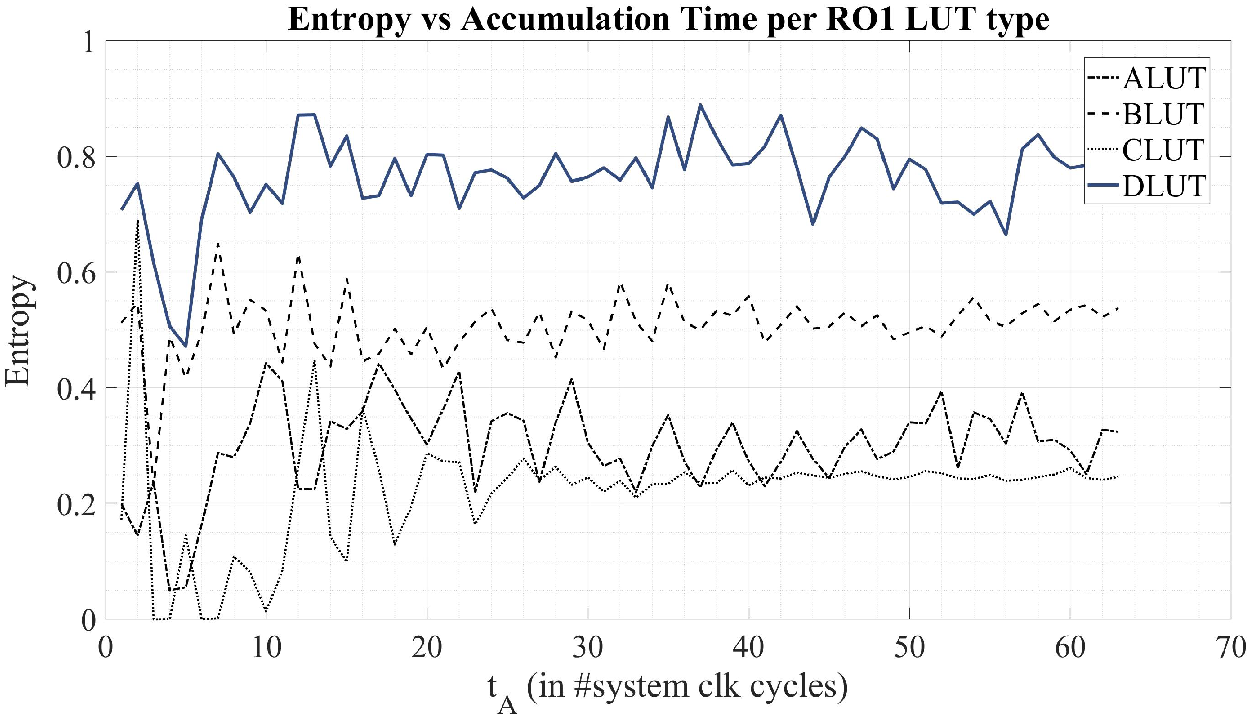
For example, for one set RO2 configuration, varying the selected LUT-type of RO1 yielded significant min-entropy deviations. Figure 4 shows the the min-entropy estimation based on the NIST test evaluation (post restart test) versus the accumulation time defined in the design. That is, we embedded a programmable construct to allow sampling after a predefined number of clock cycles of the main system clock, controlling . In this specific case, showing a set RO2, only one topology of RO1 (D-LUT) passed the NIST test with regard to the modeled entropy and the sequential test. However, there was some consistency: as the accumulation time increased, the entropy level started to stabilize when enough jitter accumulated. Nevertheless, biases in the topology and period ratios reduce the asymptotic entropy levels.
Drawing on the optimization effort and the sensitivity analysis, we chose the best {1, 3}-element configuration with a specific LUTs selection. We then examined, within a specific LUT, which input assignment produced the best results (and, hence, because we implemented simple functions, constants assignments), as well as the outcome sensitivity. As we progressed, smaller and smaller ratio differences were expected. However, to what extent and how significant was the impact on our objective criteria? Generally, LUTs are constructed from some programmable storage elements and selection-logic (equivalent to a MUX tree). However, they can be implemented with various devices/logic-topology and different layout manifestations. Together, these form the required programmable functionality. Given the unknowns mentioned above which are hard to reason and anticipate, we experimented with all possible input assignment configurations and constants settings. In Figure 5, we illustrate the min-entropy evaluation results for several examples where we set RO2 and varied the input through which the RO1 output was fed back to form the oscillator (for a 4-input LUT). There is, however, yet another degree of freedom, namely the way we assign constants to other inputs. In this case, we set all of them to be similar for a fair comparison. As shown, though the entropy variability was smaller than in Figure 4, it was still considerable, making it hard to claim robustness of the design flow with respect to design intent without exhaustive evaluation and testing.
3.2.2. Tapped-Delay Characteristics
The other key parameter that affects the resulting entropy level, and is very hard to set on an FPGA robustly with respect to the TRNG design, is the tapped delay-chain delays. We tested for the best tapped delay chain output sequence. For the same IP issues mentioned above, we tested all possible outputs of the CARRY4 to find the output order that provided a progressively increasing delay from the RO1 input to the tapped-delay outputs, as well as as inputs to the flip-flop data inputs. Though it is tempting to assume that order of arrival will increase monotonically with the tapped-delay chain output index, as illustrated at the top of Figure 6, it is, in fact, unknown because all the internal aspects are unknown to designers. Moreover, since there are differences between the rising and falling edges and different configurations which are set for each chain bit (e.g., see discussion in Reference [17]), it is challenging to derive any conclusions from digital simulation timing models for these differences with respect to a maximum-frequency driving oscillator. Denote with as the indexing of the schematic tapped delay chain. We processed the bit-extraction logic on all possible subsets of 3 taps considering the order (! options). Under the assumption that the output orders preserve the delay order, one would expect some monotonically increasing option to provide maximum entropy. Although the results were generally consistent with this intuition, i.e., {2, 3, 4} (or the equivalent {4, 3, 2}), provided the best results, for any slight imbalance, e.g., {1, 2, 3} or {1, 3, 4}, the maximal min-entropy changed dramatically. We return to the optimization of the set of delays of the taps in the ASIC optimization part of this article in the next section.
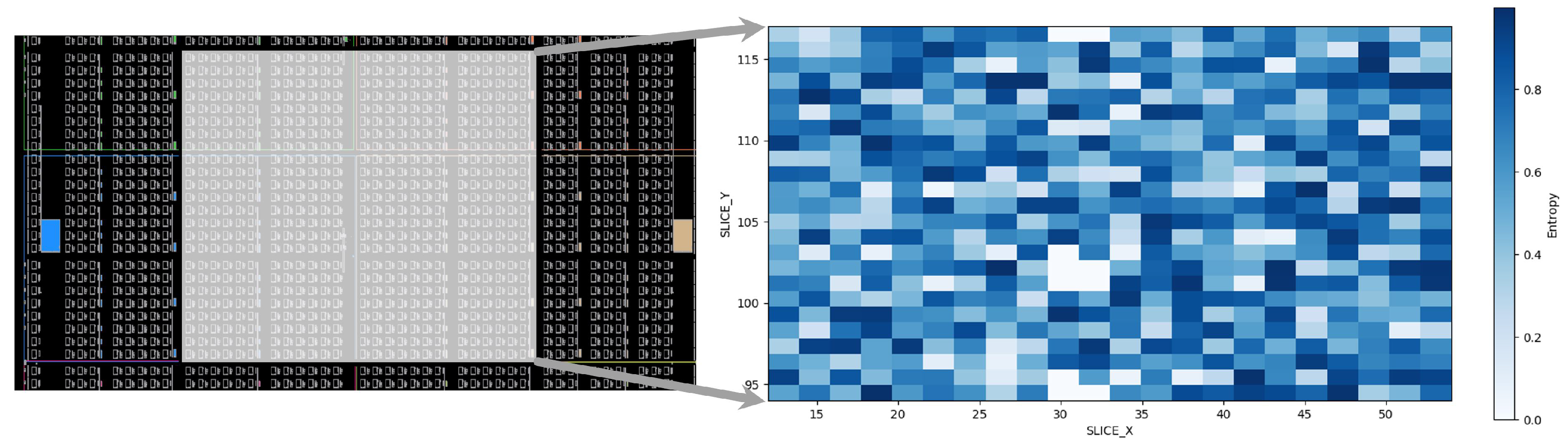
Finally, we evaluated the sensitivity of the module as a hard-macro in the design to the actual location (i.e., specific slice placed) for the best configuration. As a safeguard, we chose a long accumulation time of , represented by a counter of 7 bits, and set to 10 ns. While scanning all possible locations in a constrained area within the FPGA, we evaluated the robustness of our hard-macro to determine the variability of our objective min-entropy metric. That is, for all grid locations in the constrained area, we extracted bit-streams, collected both sequential-test ( bits) and restart-test ( bits) datasets, and calculated the min-entropy to create an “entropy map” of the device, as shown in Figure 7. We focused the evaluation on the center of the device spanning 22 × 22 slices. The experiment was repeated to verify that the map re-occurred and was stable with certainty. As shown, some patterns were visible in the map. However, there were significant variations in the min-entropy levels while changing the slices’ instantiated locations.
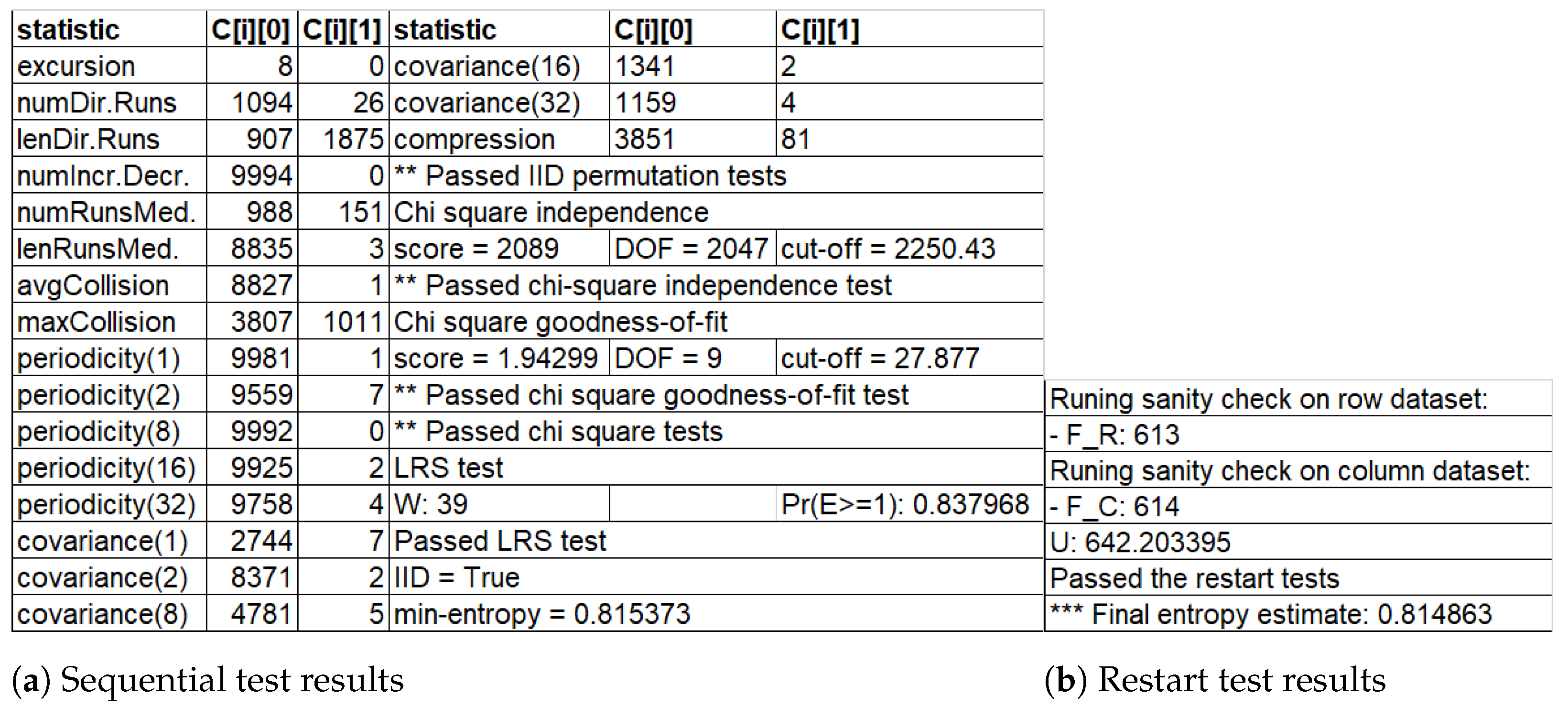
After conducting the specific optimizations, and verifying the parameters which can only be checked by measurements given uncertainty, we obtained an ES-TRNG that was carefully tailored to the specific FPGA at hand that passed the entropy tests. The entropy value of our well-tailored FPGA TRNG was ∼0.815, which was not sufficient to meet the standards without additional post-processing of the raw values (sample results from the evaluation tool output are listed in Figure 8).
3.3. FPGA Unknowns and the Hard TRNG Design Cycle
As discussed above and illustrated with various examples, FPGA unknowns inevitably induce very complex design cycles for any primitive that is not well adapted to the standard at which the device is intended to operate. Any, e.g., analog module or security-in-mind design, which imposes criteria which are not well evaluated and built-in to the design flow and optimization cycle of Computer Aided Design (CAD) tools, and specifically for FPGAs, will fall short of reaching the target criteria or achieving high certainty.
In the section above, we discussed the results from >2000 carefully designed TRNGs, all of which adhered to the same design intent. These designs were examined by post-extraction simulation, careful investigations of delay models and the tuning timing constraints of the oscillators, and, finally, by comparing the evaluated design-parameters to various methods including measurement and extrapolation. For each of the final designs, a data-collection campaign was conducted. The run time for the SP 800-90B tests for each design lasted more than a day (though faster implementations exist, e.g., in Reference [33]). We also evaluated a set of different parameters. The most time/complexity consuming one was sweeping the accumulation time, . All in all, although utilizing very high parallelism, these evaluations took ∼1-year to process. Various features emerged when pinpointing the high TRNG sensitivities in an FPGA environment, but primarily a lack of design-flow robustness in the case of non-mainstream (and modeled) design criteria. Although only one FPGA family was evaluated, to some extent, for all FPGAs, much remains unknown due to IP issues. At times, in the case of proprietary design-flows with complexities that are not always deterministic, we may not have sufficient intuitions relating to design tweaks or their actual effects. Most importantly, many parameters and characterization libraries are not well documented or accessible to designers.
As an intermediate conclusion for Section 3, with partial (FPGA only) results comparison, we refer the reader to Table 2. We note that a more general comparison with ASIC-based design results is provided in Section 5. Table 2 lists both comparable design parameters discussed above, such as , which are only relevant to compare with the prior-art ES-TRNG design. However, we also list general utilization parameters (#LUTs-, #Regs-, #CARRY4-elements) and efficiency parameters, such as entropy and bit-rates, comparable with all designs reported in the table. Several important highlights are that: (1) we only compare the raw entropy levels (no post-processing), as to provide a fair comparison; and (2) we report separately the cost of the controller part (i.e., counters and setting comparators), as these can be reduced in some designs. It is clear from the table that both the bit-rates and the entropy levels achieved surpassed the prior-art ES-TRNG design. However, as demonstrated above, this design was shown to be sensitive to numerous design parameters and was challenging to stabilize on an FPGA platform, directly motivating the next part of this paper. It can be also captured from the table that the reported TRNG is indeed the smallest in terms of FPGA resources as compared to all other designs.
4. ASIC Technology Implementation and Optimization
Many of the aforementioned weaknesses can be significantly improved with mature and flexible ASIC design flows. ASIC design-flows are more advantageous, given the level of accuracy and flexibility that can be achieved in planning. The design process is easier and more structured, which provides more control. Due to the specific nature of ASIC optimization as compared to the more general abilities of FPGAs, and the overhead caused by programmability, we can naturally expect significant improvements. In this section, we describe the implementation process of an ASIC ES-TRNG module. This is followed by a design-specific tailored optimization to increase the outcome min-entropy level and simultaneously reduce the area-utilization and energy per TRNG bit. We aimed to provide the best quantitative values, which are important ingredients for system and architectural level decisions, such as RNG selection, distribution of RNGs, etc.
We simulated the ASIC design over a transient noise simulation with a Noise parameter of 17 GHz and a Multiple Runs parameter of 32 runs. Each run was set to extract 1,000,000 random bits such that reproducibility and variance could be tested between runs with the NIST test suite. A similar simulation was done to generate data for the restart test. The simulated environment did not incorporate noise from other circuits, although these exist in real life. Therefore, this analysis is much stricter than real life, i.e., pessimistic. The design was evaluated over multiple process corners, temperatures, and voltage drops to verify robustness. In total, these high-intensity simulations took ∼7 months on a very powerful server with 50 machines, where each multi-threaded over 20 processors.
4.1. Throughput and Entropy
The randomness-throughput provided by the ES-TRNG is an outcome of two components: the accumulation time, , and the number of repeated samples needed to extract a valid raw bit. We then explore ways to minimize these components to maximize the randomness-throughput. As explained above, within the ES-TRNG architecture, signals affected by noise are sampled and encoded. The role of RO1 is to accumulate the random noise appearing in jittery behavior. The role of RO2 is to provide a clock that samples the manifestation of the noise. The role of the bit extractor is to decode the resulting view into a binary raw bit. Ideally, RO1 should produce some frequency with a duty cycle of 50%. Due to the imbalanced nature of standard-cell delays (rising versus falling transition delays), some deviation from an ideal behavior takes place. This is because the duty-cycle an oscillator produces is not necessarily 50%, and the rise and fall times can, in fact, differ. In addition, to achieve acceptable levels of randomness, RO1 needs to capture a significant amount of noise to provide sufficient entropy. In turn, it induces a long waiting period for noise accumulation, . The duration of is inversely proportional to the frequency of RO1. It can be conjectured that the faster the RO1, the more transitions will occur, thus increasing the baseline noise in the jitter. These will lead to a shorter accumulation time for a set target entropy level. However, clearly, there exists an upper bound that limits the maximum RO1 frequency. As mentioned above, RO2 provides a clock signal to sample the tapped delay chain outputs. As the RO1 frequency increases, the subsequent tapped-delay line output-sets, representing a high-resolution region, become closer. If the RO1 frequency were further increased, the high resolution areas would start to overlap. In other words, the first delayed signal would start to fall before the last one would rise, as illustrated in Figure 9. The overlap of high resolution areas reduces the total high resolution areas per cycle, which increases the accumulation time to reach the same entropy level. The upper bound on the RO1 frequency to function correctly is:
where is the period of the RO1 (fraction), the duty cycle is the duty cycle of RO1, and are the two delays of the first two delay elements’ outputs, and epsilon is an uncertainty factor which depends on the features of the technology.
One conclusion that can be drawn from this bound is that the smaller and , the higher the possible frequency of RO1, implying a minimum required accumulation time.
The second element that has an impact on the throughput is the ratio between the oscillator frequencies, as discussed above. Once the accumulation time is over, RO2 starts to sample the taps until the sample is decoded to be within the high resolution region, and a valid bit is extracted. The ratio enforces the number of RO1 cycles that take place within . At this point, it is guaranteed that we sampled in a high resolution area.
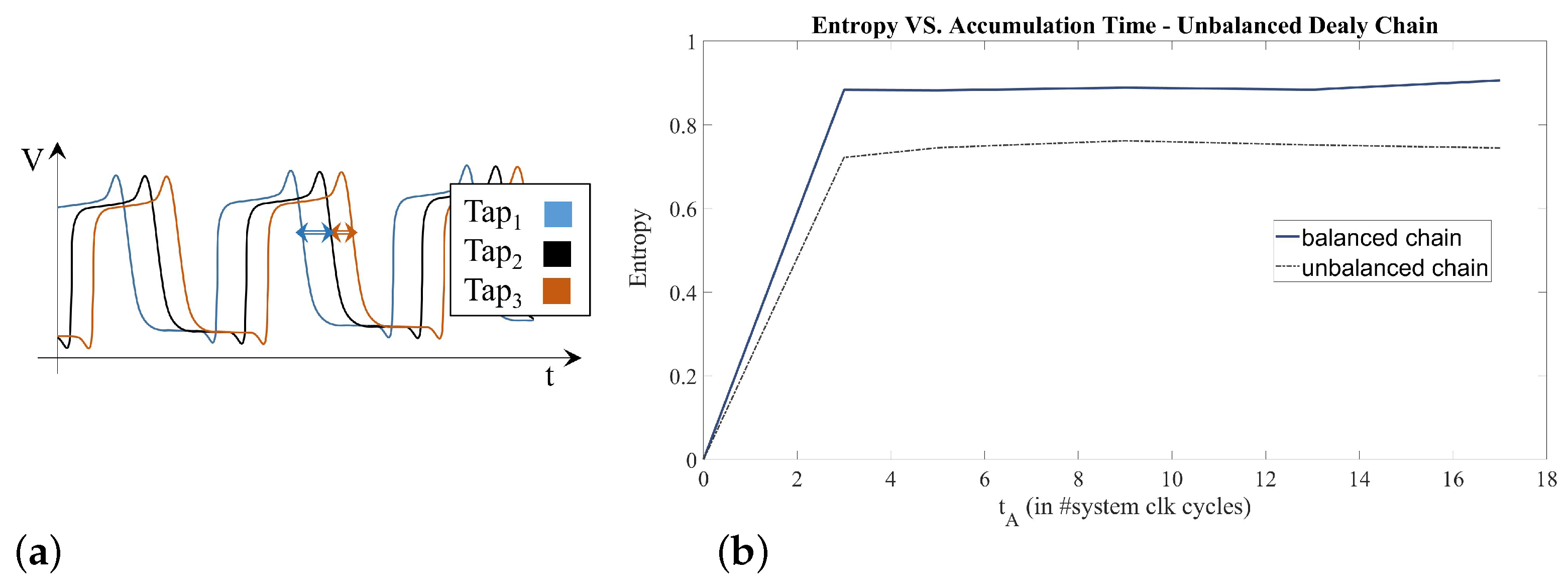
The third important parameter that affects the entropy level is the tapped delay chain, in particular, the delay difference between stages. In order to uphold a uniform distribution of raw bits, the tap delay chain loads must be balanced. With no restrictions, the first two buffers in the tap delay chain need to drive both a D-FF and the next buffer stage, whereas the third buffer only needs to drive a D-FF. However, this situation causes a mismatch in the output load along the chain, which translates into a bias, as illustrated in Figure 10a. That is, the bit extractor decodes the tapped delay chain outputs: if (decodes the valid raw of ‘1’) is not equal to (decodes the valid raw of ‘0’ ), a bias is guaranteed.
To balance the tapped delay chain, we completely balanced the output loads of the entire delay chain, while simultaneously providing ideal, minimal, and symmetric routing between the stages. The resulting min-entropy outcome is shown in Figure 10b.
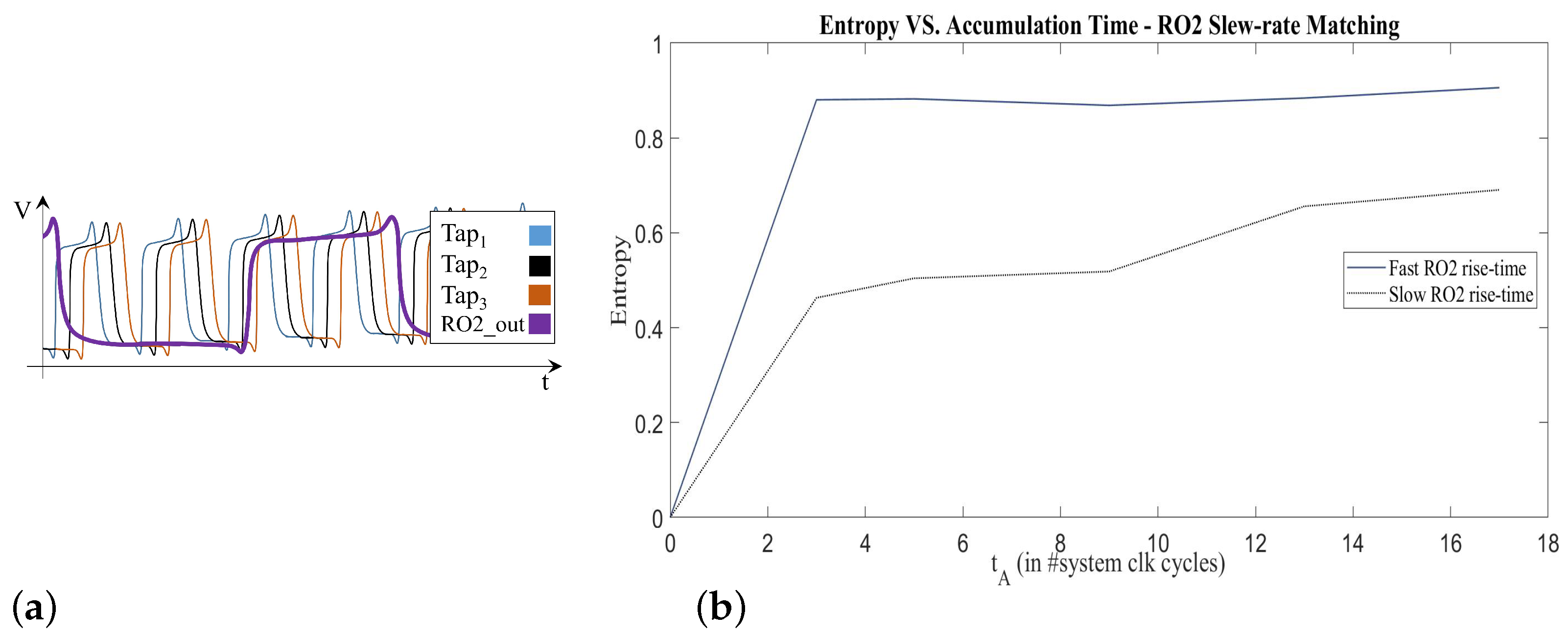
Another parameter that should be taken into account is the signals’ slew-rate (i.e., sharpness), particularly for the RO2 output signal (the sampler). If RO2’s rise time is too slow, as illustrated in Figure 11a, the sampler may not always sample a specific high resolution area (i.e., only a ‘1’ or only a ‘0’). A less than sufficiently fast mechanism may reduce the randomness throughput. Figure 11b depicts this scenario with an overly slow rise time. Although the sampler starts to rise in a high resolution area, the sampling only takes place when the RO2 output clock exceeds a certain threshold (e.g., ), capturing a low resolution area. The general rule recommended to follow is:
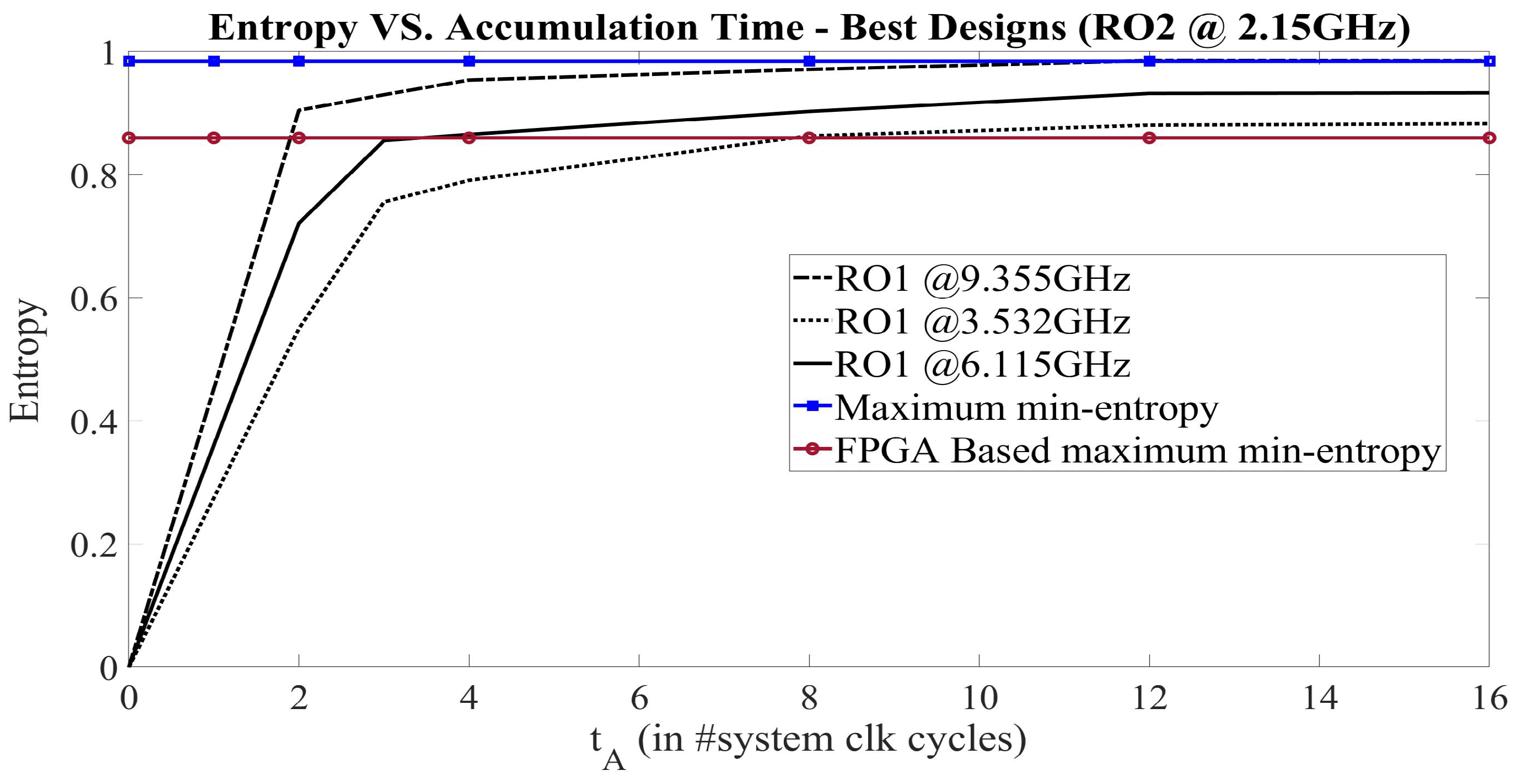
When implementing these optimization steps and a careful layout, a significant improvement from the baseline construction was achieved, as shown in Figure 12. The faster the RO1 (3 options of ∼@3.5, ∼@6.11, and ∼@9.35 GHz) for an RO2 frequency of ∼@2.15 GHz, the higher the entropy per accumulation time. The ratio set was slightly above 4/5. The red circles on the horizontal line indicate the best randomness-throughput FPGA-based ES-TRNG we were able to achieve. The x-axis intersection value with that curve shows the accumulation time needed for a fair comparison with the FPGA-based design. The best design required an accumulation time of only two cycles of the system clock, which, in our case, was set to a 10 ns period, and another two cycles of RO2 with a period of 0.46 ns. Hence, the throughput of the design was about , which was about 41.5 times higher than the FPGA-based ES-TRNG. The blue horizontal line (annotated with squares) indicates the highest entropy level captured without any pre-processing (raw) of 0.9846. At this entropy level, the required accumulation time was twelve system clock cycles and two additional RO2 cycles, providing about , which was about 7.2 times higher than the FPGA-based ES-TRNG (with smaller entropy level).
4.2. Area and Power
After evaluating and improving the design parameters that affected the min-entropy and randomness throughput, we minimized the cost factors, namely the area utilization and energy consumption of the TRNG. The design can be grossly partitioned into two main parts. The first does not impact the entropy and is negligible in terms of throughput. It includes the bit extractor and the control circuitry. The second inflicts major damage on performance in terms of both min-entropy and randomness-throughput. It includes the oscillators and the tapped delay chain. There are no special restrictions to minimize area (or, hence, energy) while meeting the timing constraints induced by the RO2 frequency. By contrast, for energy consumption, where the entropy level needs to be considered, as well, the optimization point becomes specific for each set RO1 frequency.
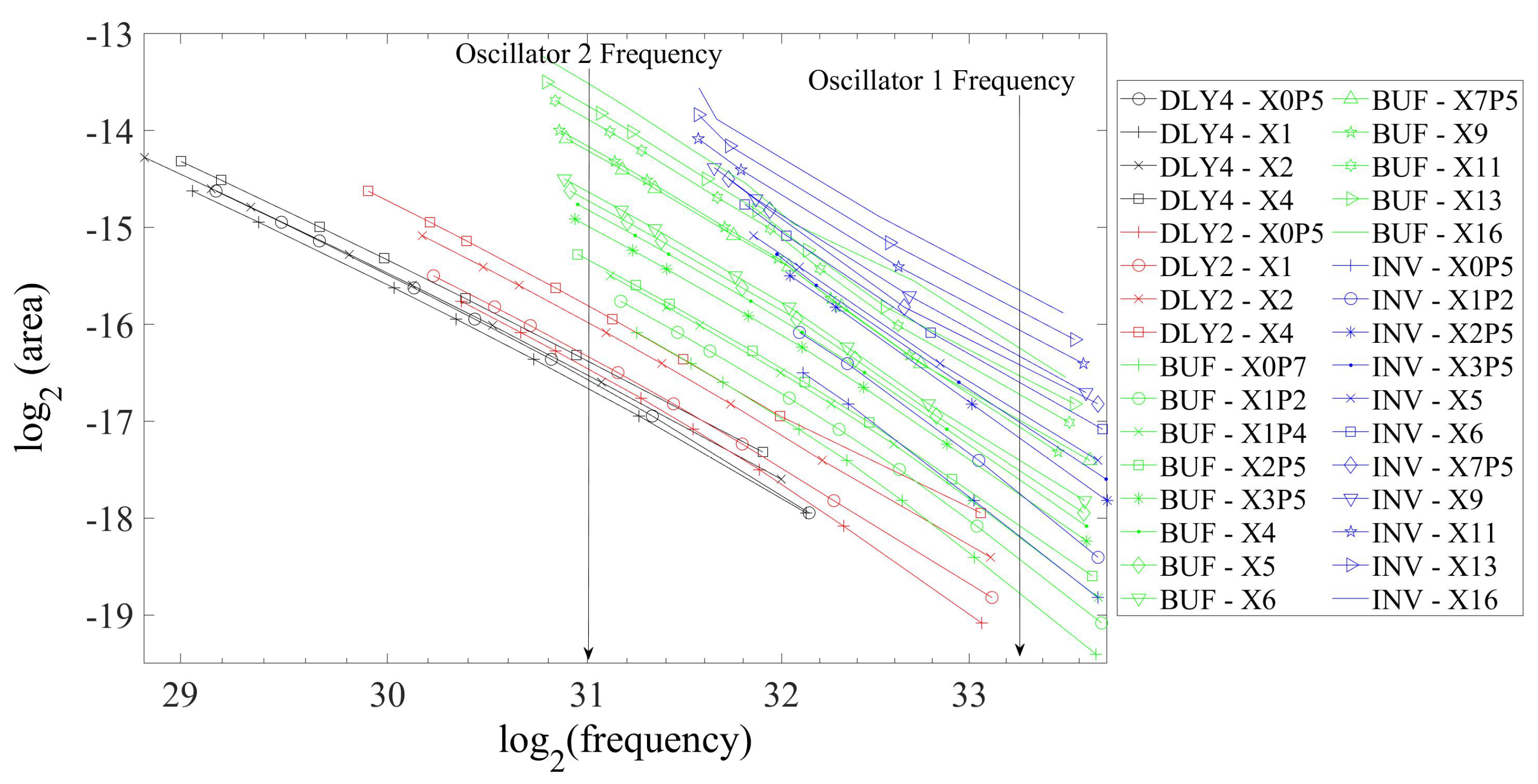
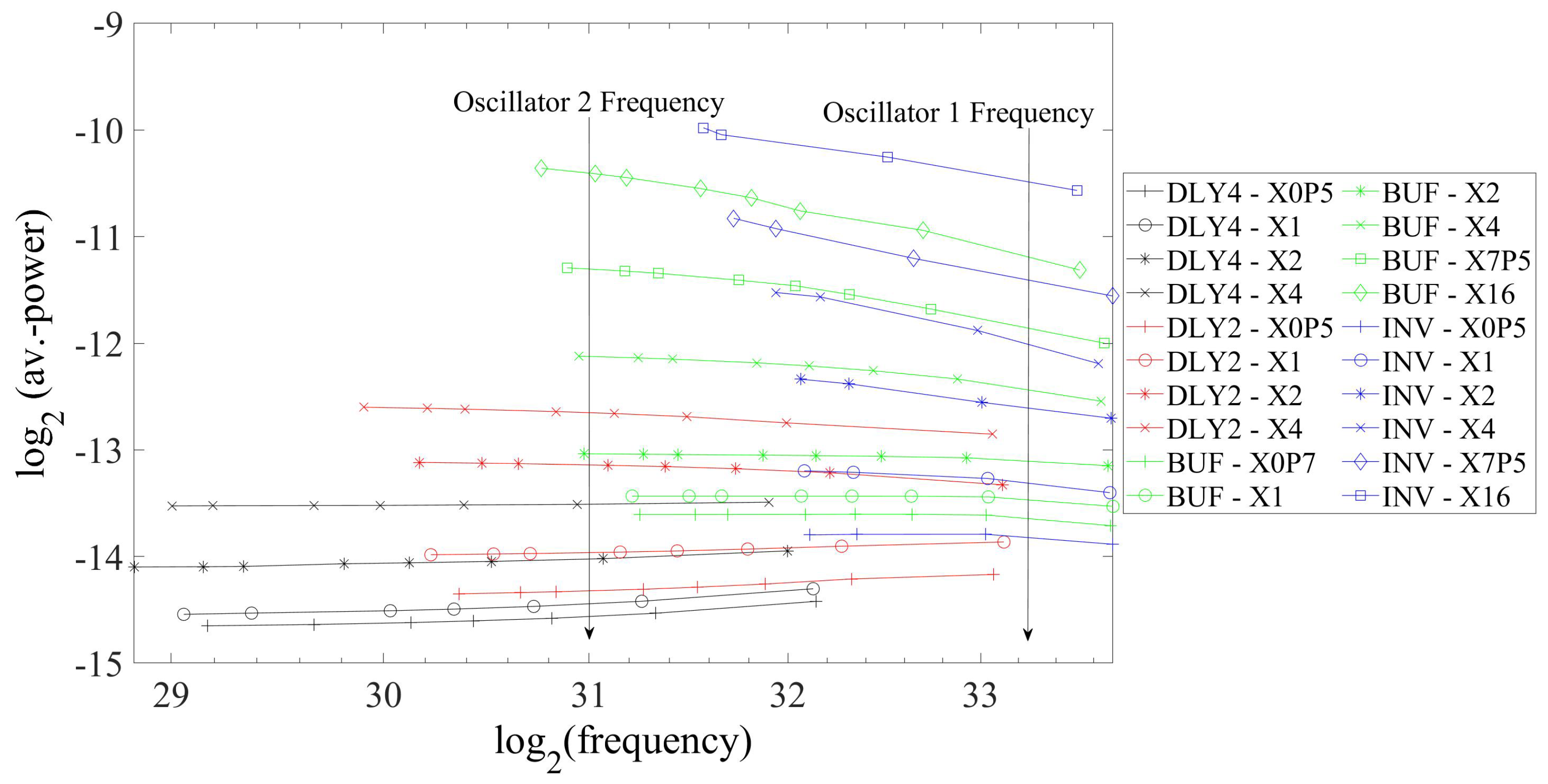
In Figure 13, we plot a general log-scale oscillator area versus its frequency. Different curves are shown to depict the oscillator using INV, BUF, DLY2, and DLY4 (delay cells) standard cells of different sizes (drive-strengths). Each type of cell has a different curve color, and each sizing factor for the same cell is depicted with a different marker. Theoretically, the curves are only bounded on the right side to adhere to the minimum of one unit in an oscillator. To achieve a specific frequency (vertical line), the intersection point with the curves indicates a possible structure for the oscillator. The minimum area with a specific frequency is obviously achieved by the lowest curve. Of interest are the overlap areas, where, for example, the largest up-sized DLY4 set overlaps with the smallest DLY2-set, etc. This is followed by the overlap of DLY2s with BUFs and BUFs with INVs. Therefore, to achieve a defined frequency, the cell library needs to be pre-analyzed. Another inherent challenge is that the number of cells is discrete; thus, the designer may need to choose larger devices or different types of cells to reach the target frequency. Within this implementation, RO1 was constructed with 1 element of size X1 of a DLY2 cell, and the RO2 with 2 cells of the smallest DLY4 element. In the specific case of a ring oscillator, the average power can be set as a reliable metric to evaluate energy consumption trends. In Figure 14, we plot the average log-scale power versus the oscillator frequency with the same set of curves, while indicating the chosen RO1 and RO2 frequencies. The same general guidelines as discussed above are used here, thus confirming that the general (rough) intuition of minimizing area utilization also minimizes energy consumption.
This device selection, which led to minimal area and power consumption, made it possible to implement the full TRNG construction with an area of 0.000252 mm and an average power consumption per bit/source of 0.1 mW for a min-entropy level of 0.86 and 1.06 mW for a min-entropy level of 0.985 (while changing the accumulation time, ).
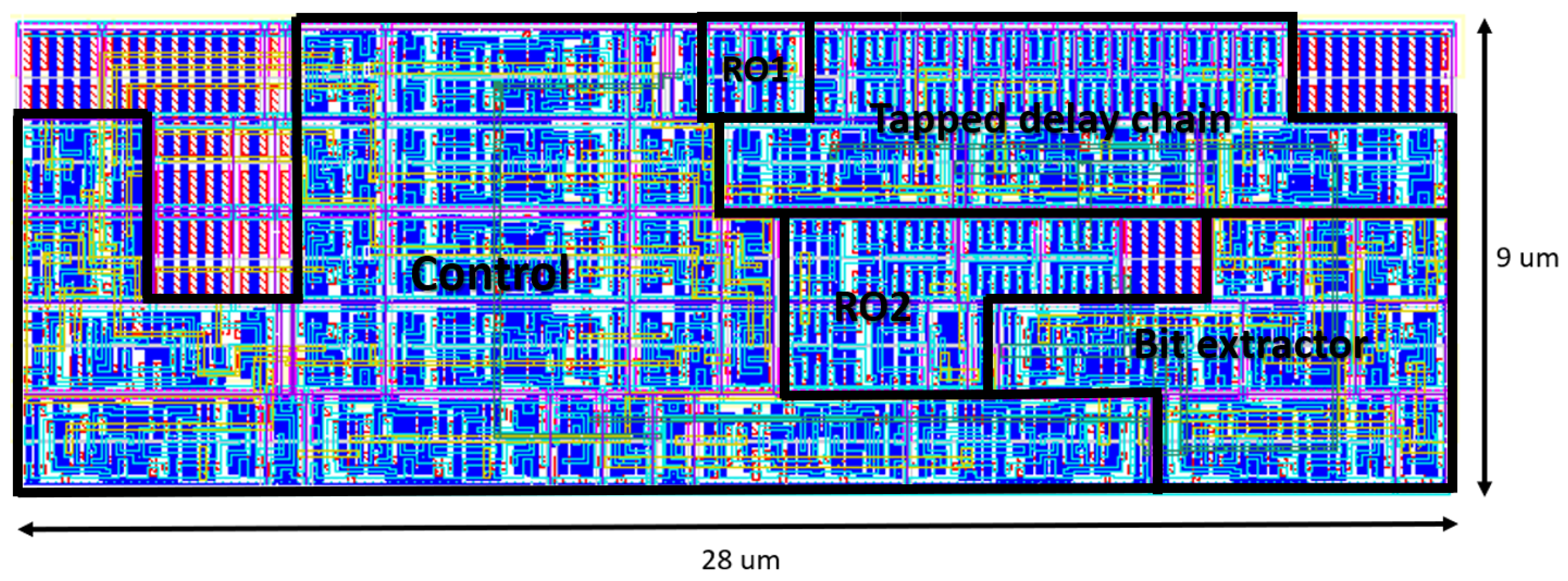
The physical layout of the TRNG is shown in Figure 15. The annotations on the figure highlight the oscillator regions, RO1 and RO2. The symmetrically routed delay line is illustrated, as fed from RO1, where the upper standard cell row is the physical delay line, and the bottom row is the registers, sampled by the oscillating signal coming from RO2. As discussed above, the output driver of RO2 which enables the small slew-rate is highly important and is placed within the RO2 region. The bit extractor logic and the rest of the control circuitry are also shown. It is important to note that (1) some of the control cost can be amortized when more than one element is placed in a design, and (2), as shown, there are several small dummy-filled regions, which were not squeezed out of symmetry considerations, but were accounted for in the total area estimation.
5. Discussion and a Test Case Analysis
We demonstrated the implementation of an ES-TRNG on an ASIC 65-nm environment which is far more robust than previous attempts at implementations and draws solely on designer-control within the ASIC design-flow. We also discussed issues related to the sensitivity of the design within an FPGA platform, backed up by measurements. However, the main contribution of this work is to provide concrete design optimization goals and design restrictions relating to: (1) the minimum and maximum delay line constraints, balancing and spacing of elements, (2) frequency targets of oscillators and the constraints they induce on the rest of the system, the magnitude of their output slew-rate in the specific context of the ES-TRNG, and (3) ways to set and minimize area/energy utilization, etc.
We began by implementing the novel ES-TRNG on an FPGA platform to test its ability to reproduce the results presented in Reference [17]. We then used ASIC technology with the same architecture and optimized the design for the area, power consumption, throughput, and entropy metrics. The optimal design achieved about 47.8 times higher throughput for the same entropy level, and about 8.27 times higher throughput for a higher entropy level of 0.985, without post-processing.
These findings were then compared to reported results from other ASIC technology-based TRNGs, as shown in Table 3, which indicates that, for each evaluation metric, a different design is preferable. We attempted to create a metric that would authorize a comparison between the different designs, as shown in Figure 16. Our objective criteria is , equally weighing both. In the figure, equal contour lines appear, and the dots represent the different prior-art (from the table). In this figure, the higher a design appears on the left, the better the overall performance. In particular, one publication [29] appears to compete with the current work, but, as can be seen, it was designed with more advanced technology (45 nm), tested to a less stringent standard, and operates on a completely different mechanism (metastable-based).
Analysis: Example of a TRNG vs. a PRNG Feeding a Lightweight Encryption Core
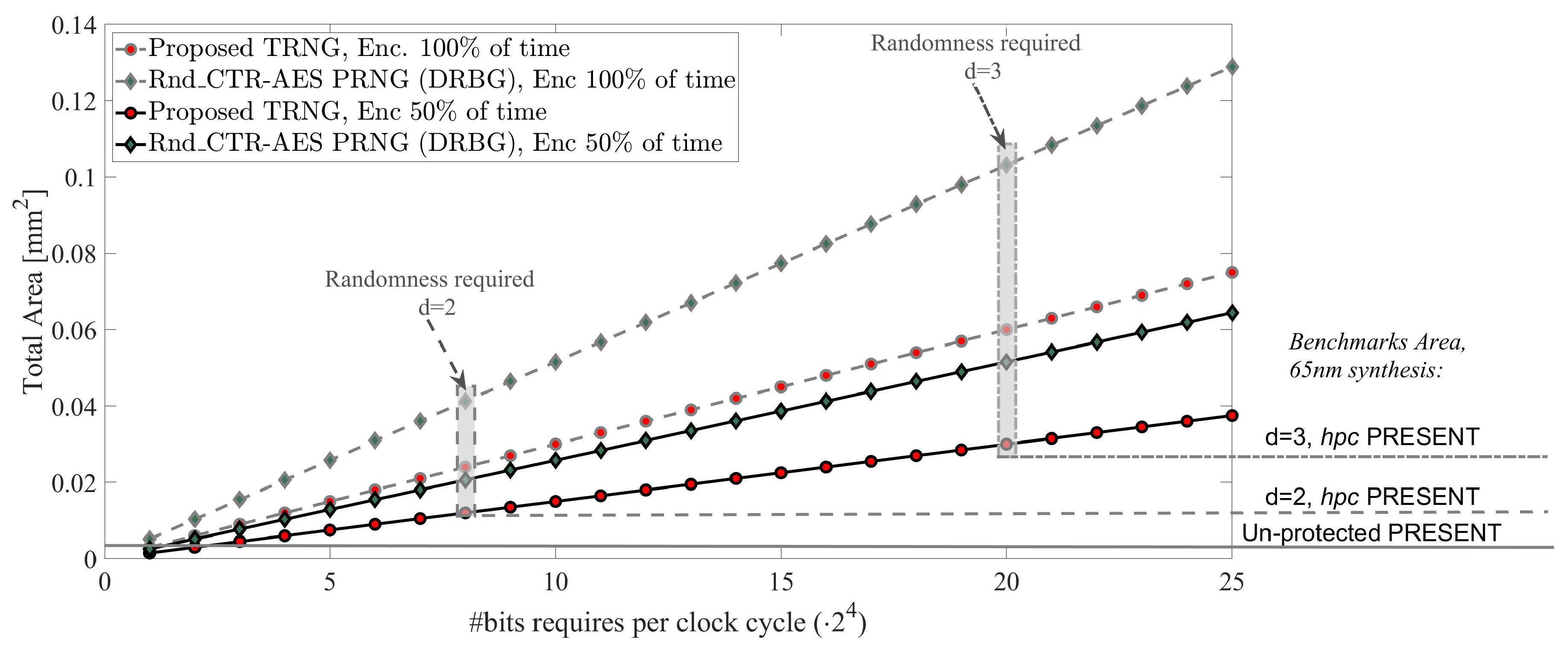
PRNG was considered according to DRBG NIST recommendations, i.e., AES in the counter mode of 128 bit per 11 cycles. We assumed a conventional clock-cycle of 100 MHz. We further excluded the cost of seeding the PRNG and the counter. TRNG units were modeled to feed randomness requiring elements in the system, while utilizing area and providing randomness throughput (RT), as discussed above.
We considered several encryption blocks: a 65-nm, synthesized, unprotected, lightweight PRESENT encryption core (corresponding to current lightweight device needs) and a hpc-masked PRESENT fully parallel rolled implementation core with , which is implemented in three clock-cycles per round [37]. Area utilization for these blocks reported from Cadence Genus 65 nm technology synthesis are denoted to the right of the figure. Clearly, randomness may be required for, e.g., SCA security of the unprotected block, using, for example, shuffling [38], amplitude-randomization [39,40,41], or it will be needed for the masked blocks which, in this case, demand or random bits per clock cycle for , 3, respectively (on average for a fully-parallel rolled implementation).
In Figure 17, we plot the total area of the PRNG (DRBG) and the TRNG versus the number of random bits they need to supply in a clock cycle (on a scale of ). We took multiple elements into consideration when parallelism was required to provide large #bits. We present two sets of curves, assuming two scenarios: when the encryption core operates continuously, 100% of the time, and when it operates only 50% of the time. This implies that random bits can be accumulated by either the PRNG or by the TRNG in the 50% case, or, alternatively, we require less parallelism (fewer RNG units, reducing the total area for the RNG).
This analysis suggests that, while utilizing the TRNG, the area cost of randomness generation is proportional to the area needed for encryption logic (when masked or alternatively randomized). However, a solution utilizing a PRNG will turn randomness generation into total-area bottleneck unless a limitation is imposed on the communication bandwidth. In low communication bandwidth applications, randomness can be accumulated or the encryption logic itself can be utilized as the PRNG building block. Therefore, in these cases, this cost factor can be amortized. However, (1) assuring low-communication bandwidth is not always possible, and it may considerably limit the application, and (2) randomness is still computational (PRNG) and more sensitive to attacks as compared to a TRNG-based solution.
6. Conclusions
Modern security systems require on-chip TRNGs. Applications demand high randomness throughput, a low area, and low energy per bit (source). Here, we evaluated the robustness and reliability of an efficient time-domain-based TRNG implementation over an FPGA platform. We demonstrated sensitivities which result in a TRNG construction that is not agnostic to electronic-design-automation tools and to designers’ know-how. We show that a considerable effort and validation are required to make designs robust, and a high degree of complexity is required from non-trivial FPGAs flows. In the second part of the manuscript, we proposed an ASIC-based implementation of the TRNG, along with the optimization steps, to enhance its characteristics. The results show that the optimized design improves randomness-throughput by 42× for the same entropy level described in previous works over the raw samples (no pre-possessing). The design simultaneously exhibits reduced energy consumption of 0.1 (mW/bit) for the same entropy level as previous works (and 1.06 (mW/bit) for a maximum entropy flavor), and the lowest area utilization of 0.000252 (mm) for a 65-nm technology evaluation. This enables the ASIC TRNGs to outperform FPGA in terms of electronic cost factors and results in the minimum Cost Per Bit/Source to date. Finally, we present a TRNG versus PRNG cost-extrapolation for security architects embedding a lightweight side-channel protected encryption core.
The simplicity of the proposed circuit, the clear optimization guidelines, large design flexibility, and control over ASIC technologies offer a high integration potential with inherent low area and power consumption, while meeting the needs for high entropy and randomness throughput.
Author Contributions
Conceptualization, I.L.; methodology, I.L. and N.K.; software, N.K.; validation, N.K., E.H. and I.L.; investigation, N.K., E.H. and I.L.; resources, I.L.; data curation, I.L. and N.K.; writing—original draft preparation, I.L. and N.K.; writing—review and editing, I.L. and N.K.; visualization, I.L. and N.K.; supervision, I.L.; funding acquisition, I.L. All authors have read and agreed to the published version of the manuscript.
Funding
This research was funded by Israel Science Foundation (ISF) grant number 2569/21.
Data Availability Statement
The data presented in this study are available in article.
Conflicts of Interest
The authors declare no conflict of interest.
References
- Panda, A.K.; Rajput, P.; Shukla, B. FPGA implementation of 8, 16 and 32 bit LFSR with maximum length feedback polynomial using VHDL. In Proceedings of the 2012 International Conference on Communication Systems and Network Technologies, Rajkot, India, 11–13 May 2012; pp. 769–773. [Google Scholar]
- Tuncer, T.; Avaroğlu, E. Random number generation with LFSR based stream cipher algorithms. In Proceedings of the 2017 40th International Convention on Information and Communication Technology, Electronics and Microelectronics (MIPRO), Opatija, Croatia, 22–26 May 2017; pp. 171–175. [Google Scholar]
- Parker, R.J. Entropy justification for metastability based nondeterministic random bit generator. In Proceedings of the 2017 IEEE 2nd International Verification and Security Workshop (IVSW), Thessaloniki, Greece, 3–5 July 2017; pp. 25–30. [Google Scholar]
- Vasyltsov, I.; Hambardzumyan, E.; Kim, Y.S.; Karpinskyy, B. Fast digital TRNG based on metastable ring oscillator. In International Workshop on Cryptographic Hardware and Embedded Systems; Springer: Berlin/Heidelberg, Germany, 2008; pp. 164–180. [Google Scholar]
- Suresh, V.B.; Burleson, W.P. Entropy extraction in metastability-based TRNG. In Proceedings of the 2010 IEEE International Symposium on Hardware-Oriented Security and Trust (HOST), Anaheim, CA, USA, 13–14 June 2010; pp. 135–140. [Google Scholar]
- Wieczorek, P.Z.; Gołofit, K. Dual-metastability time-competitive true random number generator. IEEE Trans. Circuits Syst. I Regul. Pap. 2013, 61, 134–145. [Google Scholar] [CrossRef]
- Tokunaga, C.; Blaauw, D.; Mudge, T. True random number generator with a metastability-based quality control. IEEE J. Solid-State Circuits 2008, 43, 78–85. [Google Scholar] [CrossRef]
- Srinivasan, S.; Mathew, S.; Ramanarayanan, R.; Sheikh, F.; Anders, M.; Kaul, H.; Erraguntla, V.; Krishnamurthy, R.; Taylor, G. 2.4 GHz 7mW all-digital PVT-variation tolerant true random number generator in 45nm CMOS. In Proceedings of the 2010 Symposium on VLSI Circuits, Honolulu, HI, USA, 16–18 June 2010; pp. 203–204. [Google Scholar]
- Mathew, S.K.; Johnston, D.; Satpathy, S.; Suresh, V.; Newman, P.; Anders, M.A.; Kaul, H.; Agarwal, A.; Hsu, S.K.; Chen, G.; et al. μ RNG: A 300–950 mV, 323 Gbps/W All-Digital Full-Entropy True Random Number Generator in 14 nm FinFET CMOS. IEEE J. Solid-State Circuits 2016, 51, 1695–1704. [Google Scholar] [CrossRef]
- Bucci, M.; Luzzi, R. Design of testable random bit generators. In International Workshop on Cryptographic Hardware and Embedded Systems; Springer: Berlin/Heidelberg, Germany, 2005; pp. 147–156. [Google Scholar]
- Sunar, B.; Martin, W.J.; Stinson, D.R. A provably secure true random number generator with built-in tolerance to active attacks. IEEE Trans. Comput. 2006, 56, 109–119. [Google Scholar] [CrossRef]
- Wold, K.; Petrović, S. Behavioral model of TRNG based on oscillator rings implemented in FPGA. In Proceedings of the 14th IEEE International Symposium on Design and Diagnostics of Electronic Circuits and Systems, Cottbus, Germany, 13–15 April 2011; pp. 163–166. [Google Scholar]
- Haddad, P.; Fischer, V.; Bernard, F.; Nicolai, J. A physical approach for stochastic modeling of TERO-based TRNG. In International Workshop on Cryptographic Hardware and Embedded Systems; Springer: Berlin/Heidelberg, Germany, 2015; pp. 357–372. [Google Scholar]
- Callegari, S.; Rovatti, R.; Setti, G. Embeddable ADC-based true random number generator for cryptographic applications exploiting nonlinear signal processing and chaos. IEEE Trans. Signal Process. 2005, 53, 793–805. [Google Scholar] [CrossRef]
- Cherkaoui, A.; Fischer, V.; Fesquet, L.; Aubert, A. A very high speed true random number generator with entropy assessment. In International Conference on Cryptographic Hardware and Embedded Systems; Springer: Berlin/Heidelberg, Germany, 2013; pp. 179–196. [Google Scholar]
- Fischer, V.; Drutarovskỳ, M. True random number generator embedded in reconfigurable hardware. In International Workshop on Cryptographic Hardware and Embedded Systems; Springer: Berlin/Heidelberg, Germany, 2002; pp. 415–430. [Google Scholar]
- Yang, B.; Rožic, V.; Grujic, M.; Mentens, N.; Verbauwhede, I. ES-TRNG: A high-throughput, low-area true random number generator based on edge sampling. IACR Trans. Cryptogr. Hardw. Embed. Syst. 2018, 2018, 267–292. [Google Scholar] [CrossRef]
- Petrie, C.S.; Connelly, J.A. A noise-based IC random number generator for applications in cryptography. IEEE Trans. Circuits Syst. I Fundam. Theory Appl. 2000, 47, 615–621. [Google Scholar] [CrossRef]
- Bucci, M.; Germani, L.; Luzzi, R.; Tommasino, P.; Trifiletti, A.; Varanonuovo, M. A high-speed IC random-number source for smartcard microcontrollers. IEEE Trans. Circuits Syst. I Fundam. Theory Appl. 2003, 50, 1373–1380. [Google Scholar] [CrossRef]
- Brederlow, R.; Prakash, R.; Paulus, C.; Thewes, R. A low-power true random number generator using random telegraph noise of single oxide-traps. In Proceedings of the 2006 IEEE International Solid State Circuits Conference-Digest of Technical Papers, San Francisco, CA, USA, 6–9 February 2006; pp. 1666–1675. [Google Scholar]
- Matsumoto, M.; Yasuda, S.; Ohba, R.; Ikegami, K.; Tanamoto, T.; Fujita, S. 1200 μm 2 physical random-number generators based on SiN MOSFET for secure smart-card application. In Proceedings of the 2008 IEEE International Solid-State Circuits Conference-Digest of Technical Papers, San Francisco, CA, USA, 3–7 February 2008; pp. 414–624. [Google Scholar]
- Pareschi, F.; Setti, G.; Rovatti, R. A fast chaos-based true random number generator for cryptographic applications. In Proceedings of the 2006 Proceedings of the 32nd European Solid-State Circuits Conference, Montreaux, Switzerland, 19–21 September 2006; pp. 130–133.
- Bucci, M.; Germani, L.; Luzzi, R.; Trifiletti, A.; Varanonuovo, M. A high-speed oscillator-based truly random number source for cryptographic applications on a smart card IC. IEEE Trans. Comput. 2003, 52, 403–409. [Google Scholar] [CrossRef]
- Bucci, M.; Luzzi, R. Fully digital random bit generators for cryptographic applications. IEEE Trans. Circuits Syst. I Regul. Pap. 2008, 55, 861–875. [Google Scholar] [CrossRef]
- De Roover, C.; Steyaert, M. A 500 mV 650 pW random number generator in 130 nm CMOS for a UWB localization system. In Proceedings of the 2010 Proceedings of ESSCIRC, Seville, Spain, 14–16 September 2010; pp. 278–281.
- Liu, N.; Pinckney, N.; Hanson, S.; Sylvester, D.; Blaauw, D. A true random number generator using time-dependent dielectric breakdown. In Proceedings of the 2011 Symposium on VLSI Circuits-Digest of Technical Papers, Kyoto, Japan, 15–17 June 2011; pp. 216–217. [Google Scholar]
- Amaki, T.; Hashimoto, M.; Onoye, T. A process and temperature tolerant oscillator-based true random number generator with dynamic 0/1 bias correction. In Proceedings of the 2013 IEEE Asian Solid-State Circuits Conference (A-SSCC), Singapore, 11–13 November 2013; pp. 133–136. [Google Scholar]
- Holleman, J.; Bridges, S.; Otis, B.P.; Diorio, C. A 3 μ W CMOS True Random Number Generator With Adaptive Floating-Gate Offset Cancellation. IEEE J. Solid-State Circuits 2008, 43, 1324–1336. [Google Scholar] [CrossRef]
- Mathew, S.K.; Srinivasan, S.; Anders, M.A.; Kaul, H.; Hsu, S.K.; Sheikh, F.; Agarwal, A.; Satpathy, S.; Krishnamurthy, R.K. 2.4 Gbps, 7 mW all-digital PVT-variation tolerant true random number generator for 45 nm CMOS high-performance microprocessors. IEEE J. Solid-State Circuits 2012, 47, 2807–2821. [Google Scholar] [CrossRef]
- Kokubo, H.; Yamamoto, D.; Takenaka, M.; Itoh, K.; Torii, N. Evaluation of ASIC implementation of physical random number generators using RS latches. In International Conference on Smart Card Research and Advanced Applications; Springer: Berlin/Heidelberg, Germany, 2013; pp. 3–15. [Google Scholar]
- Torii, N.; Kokubo, H.; Yamamoto, D.; Itoh, K.; Takenaka, M.; Matsumoto, T. ASIC implementation of random number generators using SR latches and its evaluation. EURASIP J. Inf. Secur. 2016, 2016, 1–12. [Google Scholar] [CrossRef] [Green Version]
- Torii, N.; Yamamoto, D.; Matsumoto, T. Evaluation of latch-based physical random number generator implementation on 40 nm ASICs. In Proceedings of the 6th International Workshop on Trustworthy Embedded Devices, Vienna, Austria, 28 October 2016; pp. 23–30. [Google Scholar]
- Sỳs, M.; Říha, Z. Faster randomness testing with the NIST statistical test suite. In International Conference on Security, Privacy, and Applied Cryptography Engineering; Springer: Berlin/Heidelberg, Germany, 2014; pp. 272–284. [Google Scholar]
- Petura, O.; Mureddu, U.; Bochard, N.; Fischer, V.; Bossuet, L. A survey of AIS-20/31 compliant TRNG cores suitable for FPGA devices. In Proceedings of the 2016 26th International Conference on Field Programmable Logic and Applications (FPL), Lausanne, Switzerland, 29 August–2 September 2016; pp. 1–10. [Google Scholar]
- Schellekens, D.; Preneel, B.; Verbauwhede, I. FPGA vendor agnostic true random number generator. In Proceedings of the 2006 International Conference on Field Programmable Logic and Applications, Madrid, Spain, 28–30 August 2006; pp. 1–6. [Google Scholar]
- Varchola, M.; Drutarovsky, M. New high entropy element for FPGA based true random number generators. In International Workshop on Cryptographic Hardware and Embedded Systems; Springer: Berlin/Heidelberg, Germany, 2010; pp. 351–365. [Google Scholar]
- Cassiers, G.; Grégoire, B.; Levi, I.; Standaert, F.X. Hardware private circuits: From trivial composition to full verification. IEEE Trans. Comput. 2020, 70, 1677–1690. [Google Scholar] [CrossRef]
- Levi, I.; Bellizia, D.; Bol, D.; Standaert, F.X. Ask Less, Get More: Side-Channel Signal Hiding, Revisited. IEEE Trans. Circuits Syst. I Regul. Pap. 2020, 67, 4904–4917. [Google Scholar] [CrossRef]
- Levi, I.; Bellizia, D.; Standaert, F.X. Beyond algorithmic noise or how to shuffle parallel implementations? Int. J. Circuit Theory Appl. Wiley Online Libr. 2020, 48, 674–695. [Google Scholar] [CrossRef]
- Levi, I.; Fish, A.; Keren, O. Low-cost pseudoasynchronous circuit design style with reduced exploitable side information. IEEE Trans. Very Large Scale Integr. (VLSI) Syst. 2017, 26, 82–95. [Google Scholar] [CrossRef]
- Levi, I.; Rudin, Y.; Fish, A.; Keren, O. Embedded randomness and data dependencies design paradigm: Advantages and challenges. In Proceedings of the 2018 Design, Automation & Test in Europe Conference & Exhibition (DATE), Dresden, Germany, 19–23 March 2018; pp. 395–400. [Google Scholar]
Figure 1.
ES-TRNG architecture.

Figure 2.
FPGA implementation, circuitry, and mapping.

Figure 3.
Measurable manipulated oscillator signals: (a) 11 LUTs ring oscillator, (b) 21 LUTs ring oscillator.
Figure 3.
Measurable manipulated oscillator signals: (a) 11 LUTs ring oscillator, (b) 21 LUTs ring oscillator.

Figure 4.
Entropy versus accumulation time per LUT input-RO1.

Figure 5.
Entropy versus accumulation time per LUT type-RO1.

Figure 6.
(a) A partial abstraction of a CARRY4 structure to derive Taps. (b) Tap ordering and entropy results.
Figure 6.
(a) A partial abstraction of a CARRY4 structure to derive Taps. (b) Tap ordering and entropy results.

Figure 7.
Entropy versus FPGA controlled location.

Figure 8.
Example for NIST test results.

Figure 9.
Taps versus RO1 frequency.

Figure 10.
Tapped delay chain optimization: (a) Unequal tapped delay chain example; (b) balanced versus unbalanced tapped delay chain-entropy.
Figure 10.
Tapped delay chain optimization: (a) Unequal tapped delay chain example; (b) balanced versus unbalanced tapped delay chain-entropy.

Figure 11.
Slew-rate optimization: (a) slow RO2 rise time example; (b) fast versus slow rise time entropy impact.
Figure 11.
Slew-rate optimization: (a) slow RO2 rise time example; (b) fast versus slow rise time entropy impact.

Figure 12.
Optimized ASIC-based design as compared to the FPGA counterpart: entropy versus tA.

Figure 13.
Oscillator area versus frequency.

Figure 14.
Oscillator power versus frequency.

Figure 15.
Full 65-nm layout of the proposed TRNG.

Figure 16.
Comparison of randomness-throughput versus area utilization per source.

Figure 17.
Total area of the proposed TRNG and an AES CNT-mode DRBG-based PRNG versus the number of needed bits per clock cycle. The values are compared to the area required to implement a PRESENT lightweight encryption without and with d = 2, 3 masking.
Figure 17.
Total area of the proposed TRNG and an AES CNT-mode DRBG-based PRNG versus the number of needed bits per clock cycle. The values are compared to the area required to implement a PRESENT lightweight encryption without and with d = 2, 3 masking.


Table 1.
Condensed comparison of the proposed TRNG as compared to the best-in-class.
| Entropy | Throughput [Mbit/s] | Area [mm] | Av.-Power [mW/Source] |
|---|---|---|---|
| -na-(Smallest known [26] 65 nm) | 0.011 | 0.0012 | 2 |
| -na-(Max. Throughput [29] 45 nm) | 2400 | 0.004 | 7 |
| 0.86 prior art-FPGA [17] | 1.15 | * | * |
| (Proposed) 0.86 | 47.8 | 0.000252 | 0.1 |
| (Proposed) 0.985 | 8.27 | 1.06 |
* Not comparable as reported over an FPGA platform.
Table 2.
FPGA-based (partial) results comparison.
| TRNG | FPGA Device | AREA (LUT/Reg/CARRY4) | Bit Rate [Mbits/s] | Entropy/bit | Entropy·Bit Rate | MHz | MHz | MHz | |
|---|---|---|---|---|---|---|---|---|---|
| ES-TRNG (Implemented) | Spartan 6 | 7/6/1 (controller): 4/9/0 | 10 | 0.815 (Raw) | 8.15 | 9 | 603.1 | 453.3 | 100 |
| ES-TRNG (prior-art) | Spartan 6 Cyclone V | 10/5/1 (controller): 6/6/0 10/6/1 (controller): 6/6/0 | 4 (no post-processing) 4.34 (no post-processing) | 0.746 (Raw) 0.746 (Raw) | 2.984 3.237 | 25 23 | 460.4 572.8 | 364.9 331.1 | 100 |
| ERO [34] | Spartan 6 Cyclone V SmartFusion 2 | 46/19/X 34/20/X 45/19/X | 0.0042 0.0027 0.014 | 0.999 0.990 0.980 | 0.004 0.003 0.013 | ||||
| COSO [34] | Spartan 6 Cyclone V SmartFusion 2 | 18/3/X 13/3/X 23/3/X | 0.54 1.44 0.328 | 0.999 0.999 0.999 | 0.539 1.438 0.327 | ||||
| MURO [11,34,35] | Spartan 6 Cyclone V SmartFusion 2 | 521/131/X 525/130/X 545/130/X | 2.57 2.2 3.62 | 0.999 0.999 0.999 | 2.567 2.197 3.616 | ||||
| PLL [34] | Spartan 6 Cyclone V SmartFusion 2 | 34/14/X 24/14/X 30/15/X | 0.44 0.6 0.37 | 0.981 0.986 0.921 | 0.431 0.592 0.340 | ||||
| TERO [34,36] | Spartan 6 Cyclone V SmartFusion 2 | 39/12/X 46/12/X 46/12/X | 0.625 1 1 | 0.999 0.987 0.999 | 0.624 0.985 0.999 | ||||
| STR [15,34] | Spartan 6 Cyclone V SmartFusion 2 | 346/256/X 352/256/X 350/256/X | 154 245 188 | 0.998 0.999 0.999 | 154.121 244.755 188.522 | ||||
Table 3.
Detailed prior-art comparison with amplitude noise-based, time-domain, and metastable-based generators.
Table 3.
Detailed prior-art comparison with amplitude noise-based, time-domain, and metastable-based generators.
| Entropy Source | Reference | Tech. | Area | Power | Throughput | Post-Proc. | Evaluation |
|---|---|---|---|---|---|---|---|
| Amplitude Noise | [18] | 2 µm | * 1.5 mm | 3.9 mW | 1.4 Mbps | - | FIPS140-1, DIEHARD |
| [19] | 0.18 µm | 0.025 mm | 2.3 mW | 5 Mbps | XOR decorr. | FIPS140-1, Knuth 2nd ed. | |
| [20] | 0.12 µm | 0.009 mm | 0.05 mW | 200 Kbps | V.Neumann | Entropy dist | |
| [21] | 0.25 µm | 0.0012 mm | 1.9 mW | 2 Mbps | - | FIPS140-2 | |
| [22] | 0.35 µm | 0.52 mm | 30 mW | 40 Mbps | - | SP800-22 | |
| Time-domain | [23] | 0.18 µm | 0.0016 mm | 2.3 mW | 10 Mbps | - | FIPS140-1, Knuth 2nd ed. |
| [24] | 90 nm | 0.006 mm | 0.24 mW | 1.74 Mbps | LFSR | AIS31, Entropy dist | |
| [25] | 130 nm | 0.2465 mm | 0.00065 mW | 25 bps | 6 bit LFSR | SP800-22 Basic | |
| [26] | 65 nm | 0.0012 mm | 2 mW | 11 Kbps | - | SP800-22 | |
| [27] | 65 nm | 0.00667 mm | - | 7.5 Mbps | - | SP800-22 Basic, DIEHARD | |
| This work (1) | 65nm | 0.00025 mm2 | 0.1 mW | 47.8 Mbps | - | SP800-90B | |
| This work (2) | 1.06 mW | 8.27 Mbps | |||||
| Metastable | [7] | 0.13 µm | 0.145 mm | 1 mW | 40 Kbps | 5:1 decimation | SP800-22 Basic |
| [28] | 0.35 µm | 0.031 mm | 0.0094 mW | 5 Kbps | NFSR | SP800-22 Basic | |
| [29] | 45 nm | 0.004 mm | 7 mW | 2.4 Gbps | - | SP800-22 | |
| [30,31] | 0.18 µm | ** 0.0018 mm | 0.27 mW | 2.5 Mbps | - | SP800-90B & -22, AIS20/31 | |
| [32] | 40 nm | 0.0188 mW | 2.5 Mbps | - | SP800-90B, AIS20/31 |
* Total die area. ** According to an estimate of the average gate size in 65 nm technology.
Publisher’s Note: MDPI stays neutral with regard to jurisdictional claims in published maps and institutional affiliations. |
© 2021 by the authors. Licensee MDPI, Basel, Switzerland. This article is an open access article distributed under the terms and conditions of the Creative Commons Attribution (CC BY) license (https://creativecommons.org/licenses/by/4.0/).
Share and Cite
MDPI and ACS Style
Klein, N.; Harel, E.; Levi, I. The Cost of a True Random Bit—On the Electronic Cost Gain of ASIC Time-Domain-Based TRNGs. Cryptography 2021, 5, 25. https://0-doi-org.brum.beds.ac.uk/10.3390/cryptography5030025
AMA Style
Klein N, Harel E, Levi I. The Cost of a True Random Bit—On the Electronic Cost Gain of ASIC Time-Domain-Based TRNGs. Cryptography. 2021; 5(3):25. https://0-doi-org.brum.beds.ac.uk/10.3390/cryptography5030025
Chicago/Turabian StyleKlein, Netanel, Eyal Harel, and Itamar Levi. 2021. "The Cost of a True Random Bit—On the Electronic Cost Gain of ASIC Time-Domain-Based TRNGs" Cryptography 5, no. 3: 25. https://0-doi-org.brum.beds.ac.uk/10.3390/cryptography5030025