Solution-Based Synthesis of Sulvanite Cu3TaS4 and Cu3TaSe4 Nanocrystals


Department of Mechanical and Materials Engineering, Florida International University, Miami, FL 33199, USA
*
Author to whom correspondence should be addressed.
Crystals 2021, 11(1), 51; https://0-doi-org.brum.beds.ac.uk/10.3390/cryst11010051
Submission received: 30 December 2020
/
Revised: 6 January 2021
/
Accepted: 7 January 2021
/
Published: 10 January 2021
(This article belongs to the Special Issue Nanostructured Crystalline Semiconductors: Structure, Morphology and Functional Properties)
Abstract
:Sulvanites have the parent formula Cu3MCh4. The metal M belongs to group 5 and Ch is a chalcogen. The tantalum sulvanites Cu3TaS4 and Cu3TaSe4 are predicted to have wide band gaps and p-type conductivity and show promise in optoelectronic applications. Their potential as p-type transparent conductors or efficient photocatalysts for visible-light water splitting is a valuable incentive to explore these materials in their nanoscale form, toward bottom-up processing opportunities. Reported herein are the first syntheses of nanosized Cu3TaS4 and Cu3TaSe4 sulvanites, which preserve the parent cubic crystal structure but show that morphology at the nanoscale is dependent of the reaction conditions. The two solution-based methods for synthesizing the tantalum S and Se sulvanites result in Cu3TaS4 or Cu3TaSe4 nanocrystals (NCs) with prismatic morphology, or, in the case of Cu3TaSe4, could lead to core-shell spherical nanostructures. The Cu3TaS4 NCs and Cu3TaSe4 NCs have good absorption in the UV-Vis region, while the Cu3TaSe4 core-shell NCs possess broad absorption bands not only in the UV-Vis but also in the near-infrared region. Photoluminescence measurements of Cu3TaS4 and Cu3TaSe4 reveal optical bandgaps of 2.54 and 2.32 eV, respectively, consistent with the values measured in bulk. Additionally, the current–voltage (I-V) curve of Cu3TaS4 NCs proves its electrical conductivity.
1. Introduction
In the last few years, the tantalum members of the sulvanites family Cu3MCh4 (M = V, Nb, Ta, Ch = S, Se) have been predicted to act as p-type transparent conductive materials (TCMs).
Defined as optically transparent and electrically conductive materials, TCMs have a wide variety of applications, from front-surface electrodes for solar cells and flat-panel displays, energy-conserving windows, rear-view mirrors with automatic dimming capability, and other optoelectrical devices to gas sensors and biosensors [1,2,3,4,5,6,7]. To date, the most common and readily accessible inorganic transparent conducting materials are transparent conducting oxides (TCOs), generally in the form of indium tin oxide (In2O3: Sn, ITO), fluorine-doped tin oxide (SnO2: F, FTO), and aluminum-doped zinc oxide (ZnO: Al), all of which have high transparency and simultaneously high n-type conductivity [1,2,8,9].
Contrary to these well-exploited n-type TCOs, the p-type TCO materials have been explored scarcely due to the difficulty in experimental preparation of p-type TCOs with both p-type doping and high hole mobilities, where the primary difficulty finally lies in the contradiction of the fundamental requirements of p-type TCOs [10]. In a standard p-type TCOs, it is desirable to provide high transparency of metal oxides while simultaneously providing high hole mobility. However, the 2p levels of the oxygen atom that dominate the valence band maximum (VBM) of the metal oxides lie far lower than the valence orbitals of the metallic atoms, resulting in the ionicity of metallic oxides, and in turn causing the strong localization of the hole at the valence-band edge, finally leading to a large hole effective mass and low hole mobility [11]. Although p-type doping of transparent conducting oxides can be accomplished by introducing holes into metal oxide materials by various doping techniques (e.g., ZnO) [12] strong localization of holes at the valence-band edge of the oxide materials and the compensation by low-energy native defects still impede the extensive exploitation of p-type TCOs [10,11,12,13]. Recently, magnesium (Mg) doping of the Cr member of the delafossites family, Mg-CuCrO2 exhibited high p-type conductivity (220 S cm−1) [14,15,16]. No other member of this family showed similar behavior, to date. Although the delafossites (CuMO2, M = Al, Ga, In, Cr, Sc) possess wide band gaps, their p-type conductivity is still not comparable to the standard n-type transparent conductive materials with the highest conductivity > 300 S cm−1 [10]. Moreover, small hole mobilities, holes high effective masses, and expensive fabrication of films with uniaxial orientation impede the further exploration of delafossites [17,18].
The sulvanites are chalcogenides, with typical semiconductor behavior. Cu3TaS4 exhibits yellow color, p-type conductivity, and wide bandgap of 2.76 eV, while Cu3TaSe4 displays light-brown color, p-type conductivity, and a bandgap of 2.36 eV [19,20,21,22,23]. In both compounds, VBM mainly originates from the hybridization of Cu 3d states and S 3p or Se 4p states, whereas conduction band minimum (CBM) is typically composed of the Ta 5d and chalcogen p states [22,24]. When compared to p-type TCOs, heavier chalcogen atom sulfur or selenium possessing higher-lying p orbitals (S 3p, Se 4p) could hybridize with the valence orbitals of Cu atom, therefore reducing the localization of holes at the valence-band edge. This in turn increases the hole mobility [14]. Furthermore, the hole effective mass of Cu3MCh4 exhibits a downward trend along the chalcogenides (Ch = S, Se), and the calculated hole effective mass of Cu3TaS4 and Cu3TaSe4 are 0.944 and 0.831 mh*, respectively [25]. The desired p-type TC should have high hole mobility, light hole effective mass, and high transparency (wide bandgap) making Cu3TaS4 and Cu3TaSe4 good p-type TC candidates [6].
Thin film TCs are usually fabricated through expensive vacuum-assisted methods. The desired replacement with solution processing methods would contribute significantly to scalability and costs reduction. Solution processing/printing methods usually require nanoscale precursors. However, there are no reports of nanostructured Cu3TaS4 and Cu3TaSe4.
To date, almost all reports about Cu3TaS4 and Cu3TaSe4 have been prepared by either solid-state methods or chemical vapor deposition [20,21,26,27,28]. Compared with the solid-state syntheses, solution-process requires low reaction temperature and is an effective approach to control the morphology and size of the synthesized materials. Furthermore, the solution process allows tailoring of nanocrystals’ solubility in a wide variety of solvents by adjusting the surfactants coated on the nanocrystals, therefore facilitating preparation of stable dispersions for further thin film deposition.
In this work, we prepared Cu3TaS4 and Cu3TaSe4 NCs using two methods and show that the final particle shape is process-dependent. In one approach a cascade synthesis involved preparation of the binary chalcogenide TaS2 or TaSe2 with 2D nanoflake morphology followed by addition of Cu cations to form the Cu3TaSe4 or Cu3TaSe4, respectively. The two processes result in nanoparticles with rectangular prismatic morphology, as showed by transmission electron microscopy (TEM), with the sulfur sulvanite NCs forming in one hour, while the selenide counterpart requiring only 10 min.
In an alternative approach, Cu3TaS4 NCs could be also synthesized through a one-pot reaction. The introduction of the sulfur source into the hot Cu-Ta cation precursor solution at 300 °C leads to cubic Cu3TaS4. The injection of Cu and Ta precursors in the sulfur solution is not possible due to the fast evaporation of CS2, used as a sulfur source. However, injection of Cu and Ta precursors into a hot selenium solution at 300 °C.is feasible and leads to a surprising core-shell morphology of Cu3TaSe4 NCs. The mechanisms of the formation of Cu3TaS4 and Cu3TaSe4 compounds synthesized through the described methods were investigated by X-Ray powder diffraction (XRD).
The specific absorption spectra of synthesized Cu3TaS4 and Cu3TaSe4 were obtained by UV-Vis-NIR.
As proof of concept, the electrical conductivity of Cu3TaS4 NCs was determined by I-V examination of printed Cu3TaS4 thin-films.
2. Materials and Methods
2.1. Materials
All chemicals used in this work were used as received without further purification. Tantalum(V) Chloride (TaCl5, 99.99%), copper(II) chloride dihydrate (CuCl2·2H2O, 99.999%), carbon disulfide (CS2, ≥99%), formamide (FA, ≥99%), oleylamine (OLA, 70%), and 1-octadecene (ODE, 90%) were purchased from Sigma-Aldrich (Saint Louis, MI, USA). Selenium powder (Se, 99.99%) and 1-dodecanethiol (1-DDT, ≥98%) were ordered from Aldrich. Sodium sulfide (Na2S, anhydrous) was purchased from Alfa Aesar. Ethanol was purchased from Decon lab. ACS grade chloroform (CHCl3, ≥99.8%) was bought from Fisher Scientific (Waltham, MA, USA). Microscope slides were bought from Globe Scientific Inc. (Mahwah, NJ, USA).
2.2. Characterization
X-ray diffraction was performed with a Siemens Diffractometer D5000 (München, (Bavaria), Germany) (Cu Kα radiation, λ = 1.5405 Å) used to determine the crystal structures of synthesized sulvanites. Raman spectra collected on the Raman Renishaw microscope (West Dundee, IL, USA) with 633 nm laser were used to determine purity of the prepared products. Philips CM200 Transmission electron microscopy (TEM) (Hillsboro, OR, USA) was used to investigate the shape and size of the synthesized TaS2, TaSe2 nanoflakes, Cu3TaS4 NCs, and Cu3TaSe4 NCs. A JEOL 6330F Scanning Electron Microscope (SEM) (Peabody, MA, USA) equipped with EDS was used at 25.0 kV accelerating voltage to determine the elemental distribution of the synthesized Cu3TaS4 NCs and Cu3TaSe4 NCs. Photoluminescence (PL) spectra of the synthesized Cu3TaS4 NCs and Cu3TaSe4 NCs were conducted on PERKIN ELMER LS-55 Luminescence Spectrometer (Waltham, MA, USA). The absorption spectra of the synthesized Cu3TaS4 NCs and Cu3TaSe4 NCs were collected using Agilent Cary 5000 UV-vis-NIR spectrophotometer (Santa Clara, CA, USA). An automated gold sputter coater (PELCO®SC-7) was used to fabricate gold electrodes on glass with 100 nm thickness and 1 cm length. The PINE Research WaveNow Potentiostat (Durham, NC, USA) was used to determine the electrical conductivity behavior of the Cu3TaS4 and Cu3TaSe4.
2.3. Preparation of TaS2 Nanoflakes
TaS2 nanoflakes were synthesized by a hot-injection method. In a glove box filled with argon gas, 1 mmol TaCl2 (358.2 mg), 9 mL OLA, and 6 mL ODE were loaded to a 100 mL of two-neck round-bottom flask sealed with a rubber septum, immediately transferred it to a Schlenk line, and then evacuated at 125 °C for 30 min. At the same time, 2 mL of 1-DDT and 3 mL of OLA were added to a 25 mL two-neck flask and stirred at room temperature under vacuum for 30 min. Afterward, the temperature of Ta precursor solution was raised to 300 °C under an argon atmosphere, at which point the S precursor solution was injected dropwise into the Ta precursor. The S precursor solution was prepared by adding 0.5 mL CS2 to a syringe containing a mixture of 2 mL degassed 1-DDT and 3 mL degassed OLA. The reaction was maintained at 300 °C for 2 h and then quenched by removing the heating source. The resulting product was washed with chloroform (CHCl3) and ethanol (C2H5OH) in a 1:3 volume ratio. (V:V, 1:3) three times, followed by drying in a vacuum oven overnight.
2.4. Cascade Synthesis of Cu3TaS4 NCs
Herein, the Cu3TaS4 NCs were prepared by the incorporation of Cu cations in to formed TaS2. In a typical synthesis, a pre-prepared Cu precursor solution was injected into the TaS2 suspension formed above at 300 °C under an argon atmosphere, and then the reaction was held at 300 °C for different times. The Cu precursor solution was made via dissolving 1.55 mmol CuCl2·2H2O (264.3 mg) into 5 mL of OLA. Afterward, the reaction was cooled to room temperature by removing the heating source. The product was washed three times with a mixture of chloroform and ethanol (V:V, 1:3). The collected precipitates were dried overnight in a vacuum oven.
2.5. Hot-Injection Synthesis of Cu3TaS4 NCs
In a typical experiment, in a glove box filled with argon, 1.5 mmol TaCl5 (537.5 mg) were added to a 100 mL two-neck round-bottom flask containing a mixture of OLA (9 mL) and ODE (6 mL). The reaction flask was sealed with a rubber septum, transferred to a Schlenk line system, and evacuated at 125 °C for 30 min, whereby a colorless, transparent solution was formed. Simultaneously, 3 mmol CuCl2·2H2O (511.5 mg) was dissolved in 5 mL OLA in a 25 mL flask and degassed at 100 °C for 30 min. 2 mL of 1-DDT and 3 mL of OLA in a 25 mL two-neck flask were degassed at room temperature for 30 min. After degassing, each of the three flasks was filled with argon. The formed Cu precursor solution was injected into the Ta precursor at 125 °C, and the reaction mixture was heated to 300 °C, where the formation of a brown, transparent solution was observed. When the Cu-Ta solution reached the target temperature, the sulfur source CS2 (0.5 mL) was added to a syringe containing a mixture of 2 mL degassed 1-DDT and 3 mL degassed OLA, and then injected dropwise into the brown Cu-Ta solution which immediately turned black. The final reaction mixture was held at 300 °C for 1 h, followed by cooling down to room temperature through removing the heating mantle. The resulting yellow product was purified with chloroform and ethanol (V:V, 1:3) three times. The obtained precipitates were dried in a vacuum oven overnight for further analysis.
2.6. Preparation of TaSe2 Nanoflakes
In a glove box, TaCl5 (1 mmol, 358.2 mg), Se (2 mmol, 158 mg), 6 mL of ODE, and 9 mL of OLA were loaded to a 100 mL two-neck round-bottom flask under argon atmosphere. This reaction flask was sealed with a rubber septum and then connected to a Schlenk line, followed by stirring for 15 min under vacuum at room temperature. Afterward, the reaction was heated to 305 °C in 30 min and then maintained at 305 °C for 1 h. Finally, cooled down the reaction to room temperature by removing the heating source. The precipitates were purified with chloroform and ethanol (V:V, 1:3) for three times.
2.7. Cascade Synthesis of Cu3TaSe4 NCs
Similar to the cascade synthesis of Cu3TaS4 NCs, the Cu3TaSe4 NCs were prepared using the pre-prepared TaSe2 nanoflakes as the starting material. In a typical synthesis, the TaSe2 nanoflakes were grown at 305 °C for 1 h, followed by injecting Cu precursor solution into the TaSe2 suspension. The reaction was further maintained at 305 °C for 1 h. The Cu precursor solution was prepared by dissolving CuCl2·2H2O (1.45 mmol, 248 mg) into 5 mL OLA. Afterward, the reaction was cooled down by removing the heating plate. The precipitates were purified with a mixture of chloroform (CHCl3) and ethanol (C2H5OH) in a 1:3 volume ratio, three times. The collected product was dried in a vacuum oven overnight for further characterization.
2.8. Hot-Injection Synthesis of Cu3TaSe4 NCs
In the hot-injection synthesis of Cu3TaSe4 NCs, the elemental Se powder was used as the Se source while TaCl5 and CuCl2 2H2O served as Ta and Cu source, respectively. In a 100 mL two-neck round-bottom flask, 158 mg Se powder (2 mmol), 9 mL OLA, and 6 mL ODE were loaded to prepare the Se precursor. The Ta precursor was prepared in a 25 mL two-neck round-bottom flask by dissolving 1 mmol TaCl5 (358.2 mg) into a mixture of 3 mL OLA and 2 mL ODE under argon atmosphere. Meanwhile, 1 mmol CuCl2·2H2O (170.5 mg) was added to a 25 mL two-neck round-bottom flask containing 5 mL OLA to make the Cu precursor solution. Each of the three precursors was degassed at 120 °C for 30 min and then flushed with argon. Next, the Cu precursor solution was injected into the Ta precursor and then maintained at 120 °C to form a brown Cu-Ta solution. In parallel, the Se precursor was heated to 300 °C, and the Cu-Ta solution was injected immediately into the Se solution. An immediate black color change was observed (within one second). The reaction mixture was held at 300 °C for 1 h. Afterward, the reaction was quenched by removing the heating source. The product was washed with a mixture of chloroform and ethanol (V:V, 1:3) three times, collected, and dried in a vacuum oven overnight.
2.9. Fabrication of Cu3TaS4 NCs and Cu3TaSe4 Inks
Cu3TaS4 inks were prepared by dispersing 30 mg of Cu3TaS4 NCs into 1 mL of ethanol using probe ultrasonication for 20 min. Cu3TaSe4 inks were prepared by the same dispersion method. Each ink was prepared from NCs that were subjected first to ligand exchange, toward removing residual OLA remaining on the NCs surface from synthesis and replace them with S2−. The ligand exchange of Cu3TaS4 NCs and Cu3TaSe4 NCs followed a previously reported process for Cu3VSe4 NCs [29]. In a typical experiment, Cu3TaS4 NCs were suspended in chloroform (8 mg/mL). Then, 10 mL of this suspension was transferred to a 50 mL tube containing 10 mL of Na2S solution in formamide (0.2 M). Next, the mixture was vigorously shaken for 1 min and further allowed to rest until ligand exchange completion, when Cu3TaS4 NCs were fully transferred from the chloroform phase (lower) to the formamide phase (upper). Afterward, the clear chloroform phase was removed, and 5 mL distilled water and 20 mL of ethanol was added to the aqueous phase to precipitate the Cu3TaS4 NCs. The precipitate was purified by washing it twice with a mixture of ethanol and distilled water (ethanol:water = 4:1) followed by washing with a mixture of toluene and ethanol (toluene:ethanol = 1:3). The resulting product was collected and dried in a vacuum oven overnight. The same process was followed for Cu3TaSe4 NCs ligand exchange.
2.10. Fabrication of Cu3TaS4 NCs and Cu3TaSe4 NCs Thin Films and Devices
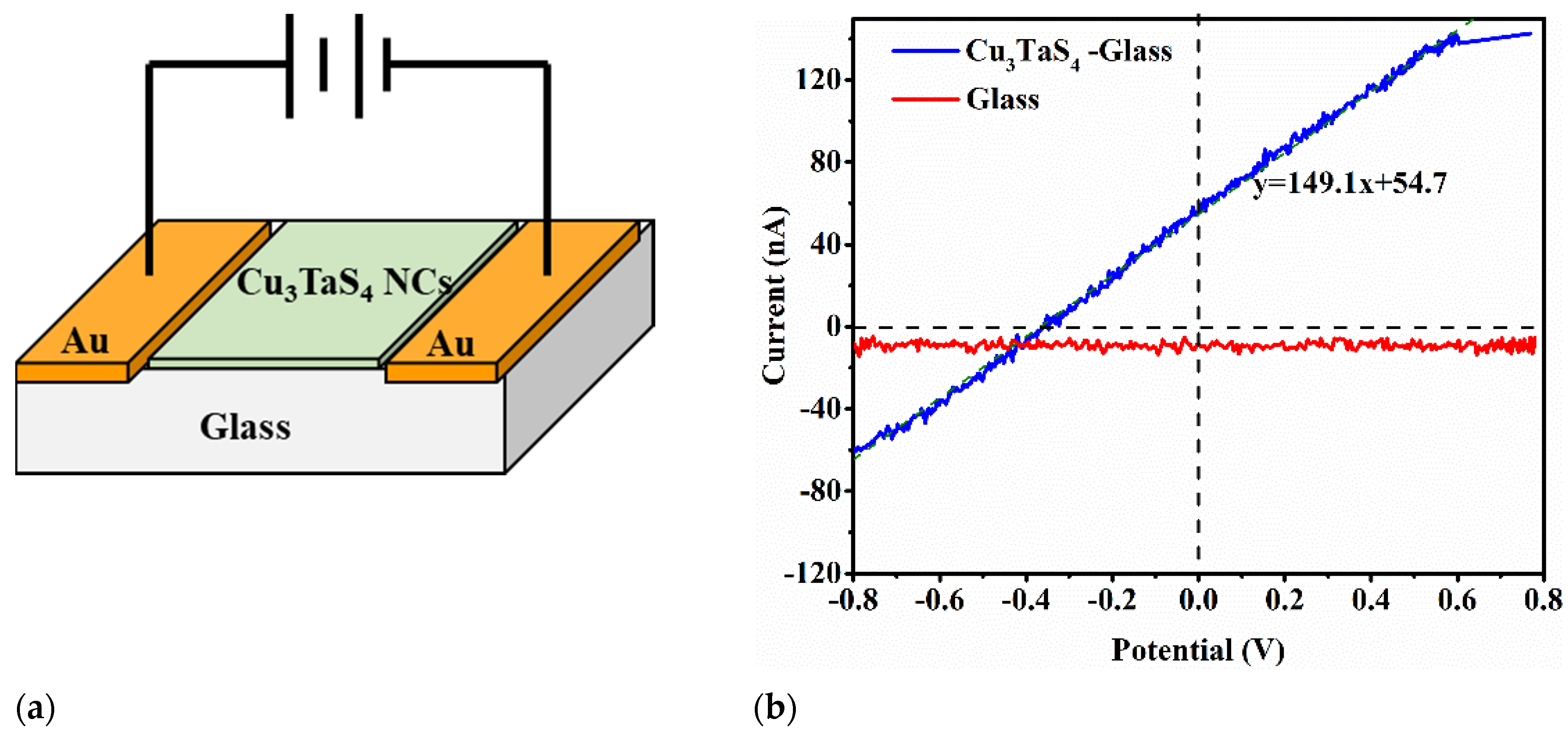
To evaluate the electrical conductivity of the Cu3TaS4 NCs and Cu3TaSe4 NCs, thin films were fabricated with each of the NCs on glass, as follows. First, the glass slides were washed with distilled water, acetone, and methanol in sequence for 5 min each solvent, using an ultrasonic bath. Then, gold was coated on a clean glass substrate by using an Au sputter coater to fabricate two gold electrodes with a thickness of 100 nm and a width of 1 cm, leaving a separation of 1 cm between two Au electrodes. Afterward, an amount of 10 μL of Cu3TaS4 or Cu3TaSe4 inks (30 mg/mL) was coated to the inter-electrode gap by bar-coating (as depicted in Figure 7a. The thin film was dried in air at 100 °C for 1 min using a hot plate. The coating and drying process was repeated twice to manufacture the Cu3TaS4 NCs and Cu3TaSe4 NCs-based devices.
3. Results and Discussion
3.1. TaS2 Nanoflakes Characterization
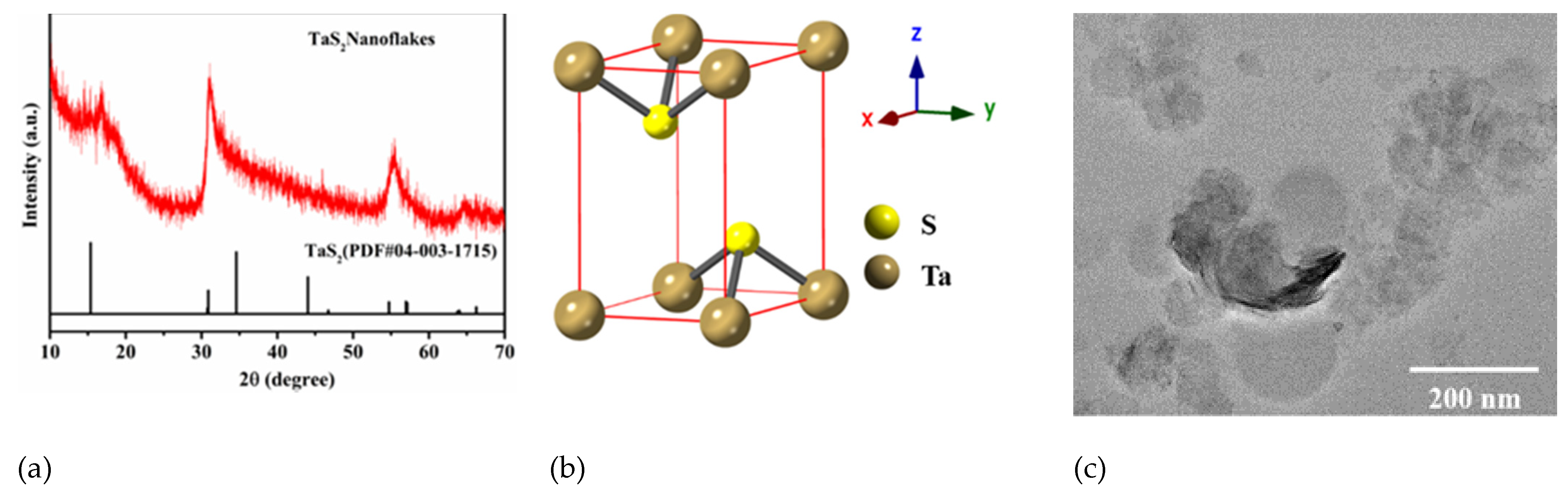
The crystal structure of the synthesized TaS2 was identified from the XRD pattern shown in Figure 1a, exhibiting two characteristic peaks at 30.6 and 54.6 degrees, which could be indexed to the hexagonal TaS2 phase (PDF# 04-003-1715) with a space group of 3m1. It is worth noting that the peak intensity ratio of the synthesized TaS2 is not the same as the indexed pattern which could be attributed to the preferential growth of the two-dimensional (2D) nanostructures in specific crystallographic directions with a high aspect ratio. Figure 1b illustrates the crystal structure of TaS2. A low-magnification TEM image of the synthesized TaS2 is showed in Figure 1c. Notably, the TaS2 exhibit thin nanoflake morphological features, with nanosheet size ~150nm in diameter. A stacking of the nanoflakes is observed.
3.2. Cu3TaS4 NCs
3.2.1. Characterization of Cu3TaS4 NCs
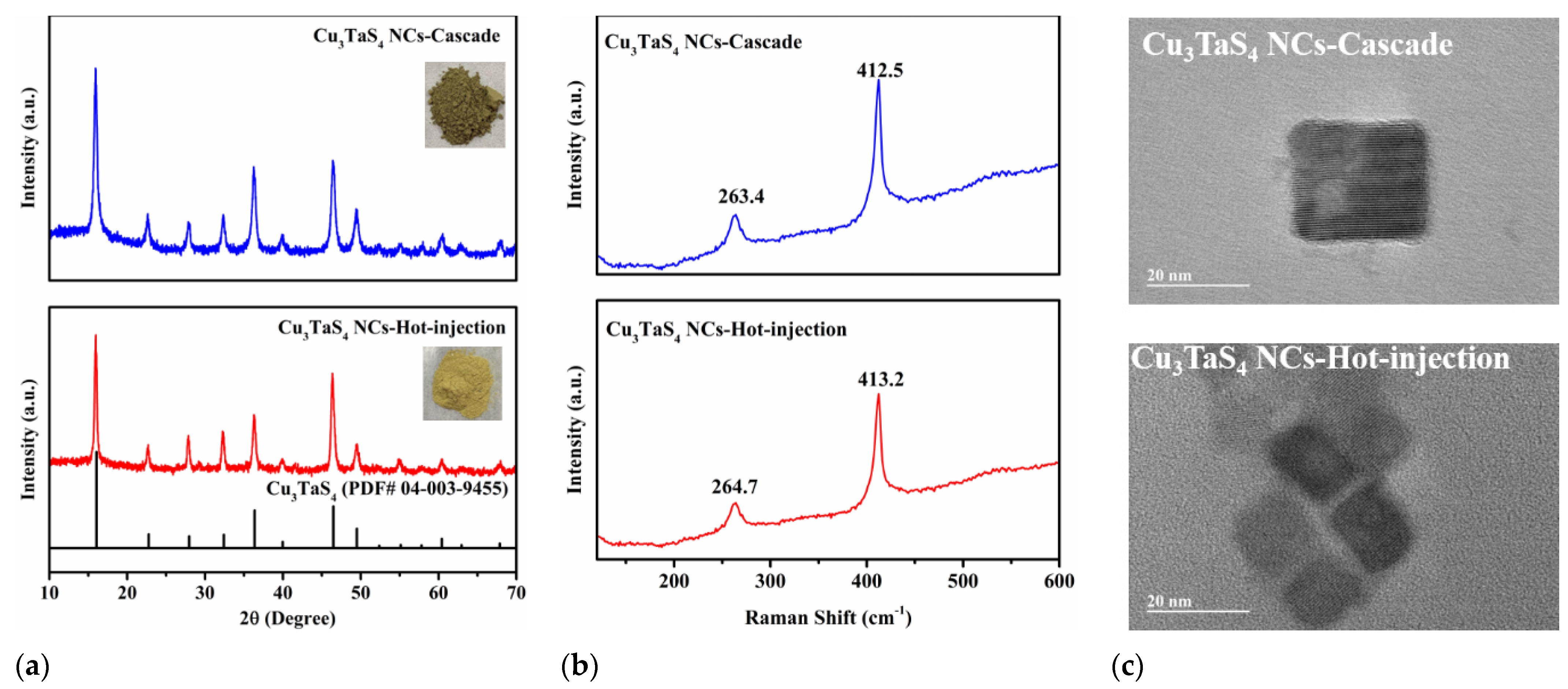
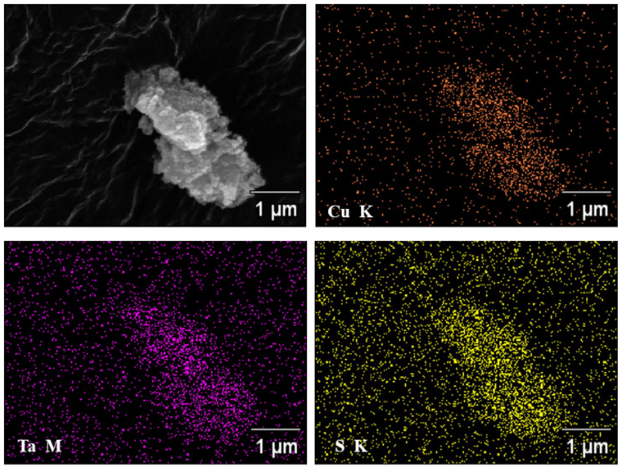
XRD patterns of the products prepared using either the cascade method or the hot-injection method (Figure 2a) shows a single cubic Cu3TaS4 phase with a space group of P43m, however, the product colors are different: Cu3TaS4 NCs (inset) synthesized using hot-injection is yellow, while the Cu3TaS4 NCs synthesized using the cascade method, displays a mustard-green color. Through investigating Cu3TaS4 NCs prepared with different amounts of Cu incorporation, we speculated that the variety in the color of the products should be caused by different amounts of Cu insertion. In the hot-injection synthesis of Cu3TaS4 NCs, when we added the Cu, Ta, and S precursors with stoichiometric ratio, the obtained product showed dark green and a mixture of Cu2S and Cu3TaS4 phases, as shown in supporting information (Supplementary Materials Figure S1). A comparison of Raman spectrum of the Cu3TaS4 NCs synthesized using cascade method and hot-injection in Figure 2b shows two identical dominant Raman scattering peaks at around 264.1 cm−1 and 413 cm−1, which correspond to the A1 mode of Cu-S bond and A1 vibration mode of Ta-S bond of Cu3TaS4, respectively, in good agreement with the previous reports [30]. Our recent report showed that a cascade synthesis of Cu3VSe4 from VSe2 nanosheets leads to a preservation of nanosheet morphology [31]. In this light, it was expected that Cu3TaS4 formed using the same method will facilitate the preservation of nanosheets. However, Cu3TaS4 was formed in cubic shape with an average size of around 20 nm (Figure 2c), without maintaining the 2D morphology of the TaS2 nanoflakes template. Earlier reports show such example of the transformation from nanosheets to nanodisks upon adding the third cation, in the case of CuInS2 [32]. Ultrathin γ-In2S3 nanosheets were turned into CuInS2 nanodisks when incorporating the Cu+ ions. In this case it was hypothesized that the reason for the formation of CuInS2 nanodisks from γ-In2S3 nanosheets during colloidal synthesis is that the incorporation of Cu+ caused additional strain, which will lead the folded nanosheets to tear into nanodisks [32].Thus, we posit that the insertion of Cu cations during the preparation of Cu3TaS4 NCs by cascade method caused additional stress which resulted in tearing of the folded TaS2 nanoflakes into cubic nanocrystals in the solution process. Similarly, the TEM image (Figure 2c) of the Cu3TaS4 NCs prepared by hot-injection presents cubic shape with a smaller particle size of ~15 nm. The SEM-EDS elemental mapping of the synthesized Cu3TaS4 using the cascade method (Figure 3) shows a homogeneous distribution of Cu, Ta, and S elements.
3.2.2. Mechanism of Cu3TaS4 NCs Cascade Synthesis
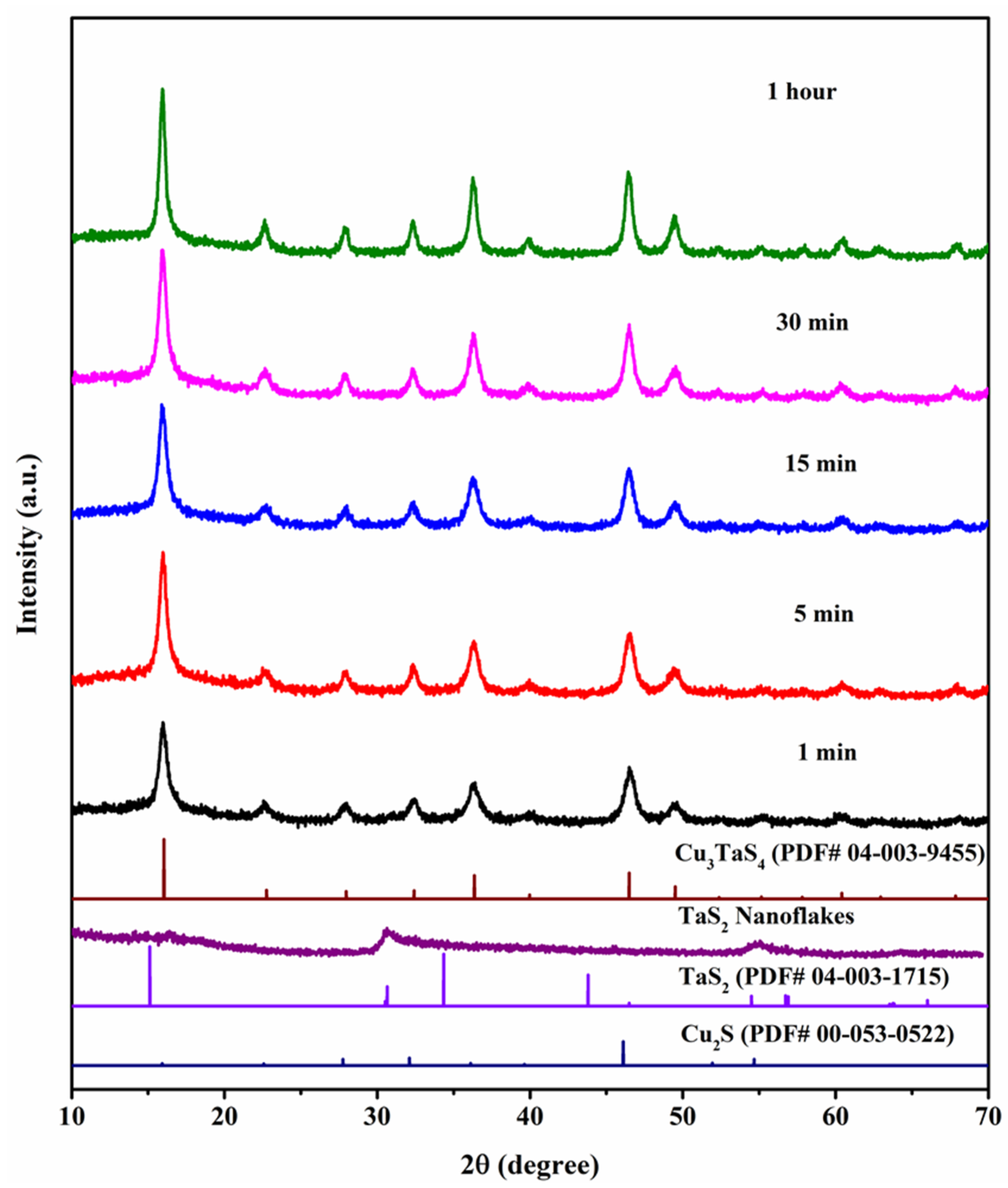
To get an insight into the mechanism of Cu3TaS4 NCs formation through cascade synthesis, a series of experiments with different reaction times were carried out, and the XRD patterns of the obtained products (Figure 4) were used to investigate the phase transformations during the process. Upon the addition of Cu cations to the formed TaS2 nanoflakes, a rapid phase transition from hexagonal TaS2 to cubic Cu3TaS4 happened, which was observed to occur within 1 min. Additionally, when extending the reaction time to 1 h, neither secondary phase nor other crystalline impurities were detected, however, the color of the products gradually changed from black to yellow, and the crystallinity and yield of products were enhanced. The color changes of the product with the reaction time are detailed in the Supplementary Figure S2a. The phase transformation identified by XRD patterns proved that there was a major rearrangement of atoms in the TaS2 nanoflakes when inserting Cu cations. Herein, the ultrathin template of TaS2 nanoflakes was considered to be the key to the rapid synthesis of Cu3TaS4 nanocrystals, since the large surface area and high aspect ratio of the 2D nanostructures provide more reaction sites, thereby promoting the migration of Cu cations and rearrangement of atoms, which finally accelerates the formation of Cu3TaS4 nanocrystals.
3.2.3. Mechanism for Hot-Injection of Cu3TaS4 NCs
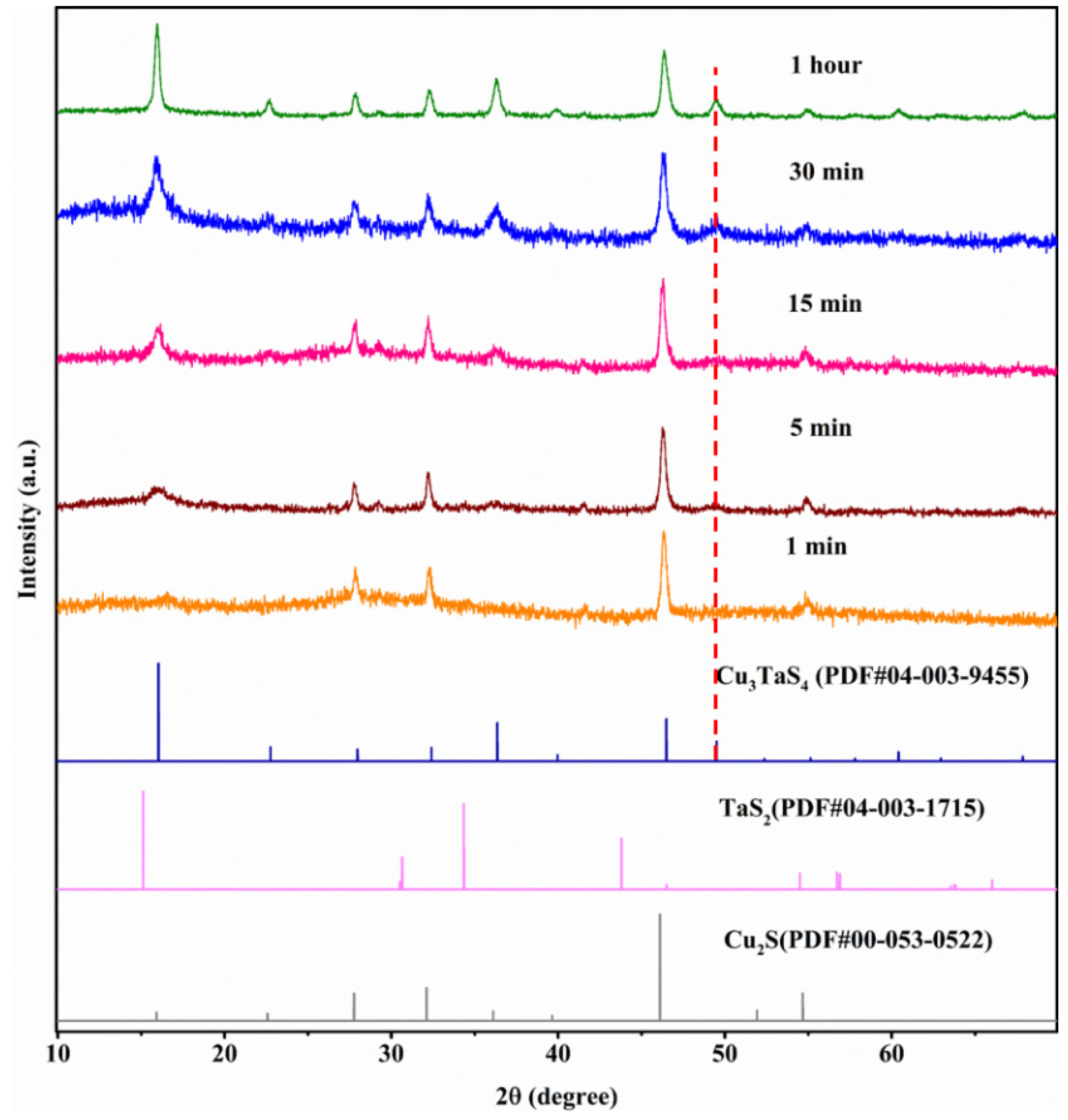
Briefly, the hot-injection method involves the injection of a cold reagent into hot precursors to trigger rapid nucleation which is followed by a crystal growth step. Figure 5 compares the XRD patterns of the Cu3TaS4 NCs products obtained at different reaction times after adding the sulfur source. The color changes of the products are shown in the Supporting Information (Supplementary Materials Figure S2b). Given that the primary XRD peak positions of the Cu2S (PDF# 00-053-0522) are close to those of Cu3TaS4 (PDF# 04-003-9455), we considered the distinguished peak at 49.5° 2θ (marked by the red dotted line) to be the indicative of the presence of the Cu3TaS4. As shown in Figure 5, 1 min after adding the S source into the Cu-Ta precursors, the XRD of the product showed a Cu2S phase. As noted above, after 30 min, a characteristic peak at 49.5° 2θ appeared in the XRD pattern, indicating the formation of the cubic Cu3TaS4 phase. As the reaction progressed, the XRD peaks intensity of Cu3TaS4 gradually increased; at 1 h the intensity of peak at 16.04° grew relatively higher than that of 46.5°, where the peak intensity ratio of 16.04° to 46.5° is close to the indexed patten, indicating the formation of pure phase of Cu3TaS4. Thus, in the hot-injection synthesis of Cu3TaS4 NCs, the swift addition of the sulfur precursor into the Cu-Ta metal precursor at 300 °C triggered the rapid nucleation of Cu2S seeds, and then the formed Cu2S seeds subsequently reacted with Ta cations to form the Cu3TaS4 nanocrystals. Compared with the cascade synthesis of Cu3TaS4 NCs that uses TaS2 nanoflakes as the starting templates, the hot injection method which employs the formed Cu2S as the starting seeds took a longer time to form Cu3TaS4 NCs. We attribute this to the larger radius of Ta cation.
3.2.4. Optoelectrical and Conductive Properties of Cu3TaS4 NCs
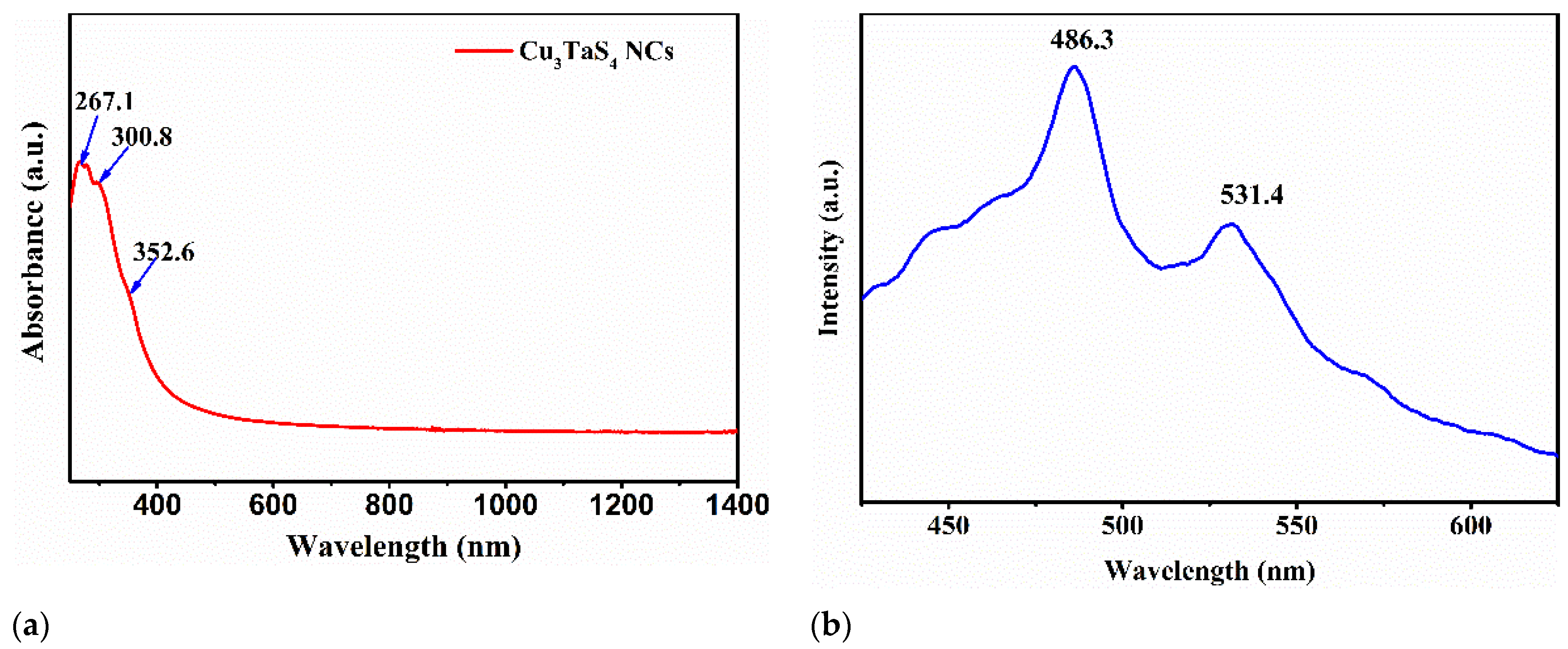
Figure 6a depicts the optical absorption spectrum of the synthesized Cu3TaS4 NCs in the ultraviolet, visible, and near-infrared regions, which shows three absorbance bands at around 267.1, 300.8 and 352.6 nm. Figure 6b shows the photoluminescence (PL) spectrum of the synthesized Cu3TaS4 NCs in ethanol, when using 360 nm as the excitation wavelength, the characteristic emission peaks occurred at 486.3 and 531.4 nm, corresponding to 2.54 eV and 2.33 eV, respectively. The green emission at 531.4 nm indicated a mid-band-gap charge trap caused by Cu vacancies near the valence band maximum, in good agreement with a previous report by Hersh [21], where green photoemission at 548 nm was present for the Cu3TaS4 single crystal.
To evaluate the electrical conductivity of the Cu3TaS4 NCs, a Cu3TaS4 NCs-based device with a configuration of Au/Cu3TaS4 NCs-glass/Au was subjected to an I-V measurement. The schematic of the device configuration for the I-V measurement is shown in Figure 7a. The I-V curve of the Au/Cu3TaS4 NCs-glass/Au device is shown in Figure 7b blue line, where the current progressively increases along with the voltage bias towards positive, implying the electrons could flow through the Cu3TaS4 NCs area. Generally, glass is a good insulator that does not allow the flow of electrons, and its conductivity is negligible as compared to the material of the thin films. Thus, it could be concluded that in the Au/Cu3TaS4 NCs-film/Au device, the electrons flow through the Cu3TaS4 NCs thin film rather than the glass substrate. To prove our hypothesis, we prepared a control device configured as Au/Glass/Au, where the two gold electrodes connected only by clean glass. The I-V curves of the control device are shown in Figure 7b red line, where the current is kept at around zero amperes when increasing the voltage, suggesting that no electrons flow through the glass substrate, which further evidence our hypothesis that Cu3TaS4 material has electrical conductivity. The obtained I-V plot of the Au/Cu3TaS4 NCs-glass/Au device allowed us to calculate the electrical conductivity of Cu3TaS4 NCs. Using the equation R = V/I (R-Resistance in ohms(Ω); V-voltage in volts (V); I-current in amperes(A)), we could calculate the resistance of Cu3TaS4 NCs, namely, the slope of the I-V curve, which is 1.49 × 10⁷ Ω. Generally, the electrical conductivity of a thin film (σ) could be determined using the following expression:
where R is the film resistance between the two electrodes, t is the thickness of the sample, and A is the surface area of the sample [33,34,35,36,37,38,39]. Here, R is 1.49 × 10⁷ Ω, t is 2.05 ∗ 10−6 m (determined from SEM cross-section of the film), and A is 10−4 m2, thus, the calculated electrical conductivity of Cu3TaS4 NCs is 1.38 × 10⁻⁹ S·m−1. Although the calculated electrical conductivity is low, this could be attributed to a poor quality of the thin film and poor connection between Au electrodes and Cu3TaS4 NCs thin film. The optoelectronic properties of Cu3TaS4 NCs suggests that the materials are a promising candidate for the p-type transparent conductor applications.
3.3. Characterization of TaSe2 Nanoflakes
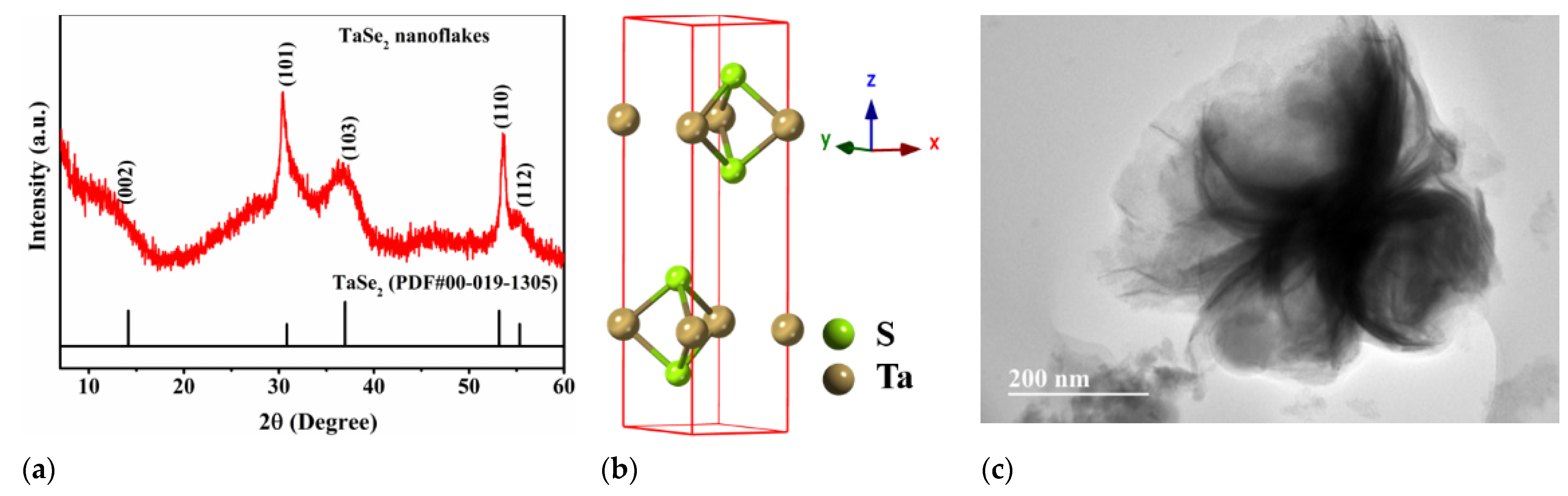
The crystal structure of the synthesized TaSe2 was analyzed by powder XRD pattern as shown in Figure 8a, which is in good agreement with the patterns reported by Jeong at. Al [40], where they assigned the product to the hexagonal TaSe2 phase (PDF# 04-019-1305) with a space group of P 63/mmc. The identified crystal structure is shown in Figure 8b. The TEM image shown in Figure 8c indicates the folded nanoflakes characteristic of the solution synthesized TaSe2.
3.4. Cu3TaSe4 NCs
3.4.1. Characterization of Cu3TaSe4 NCs
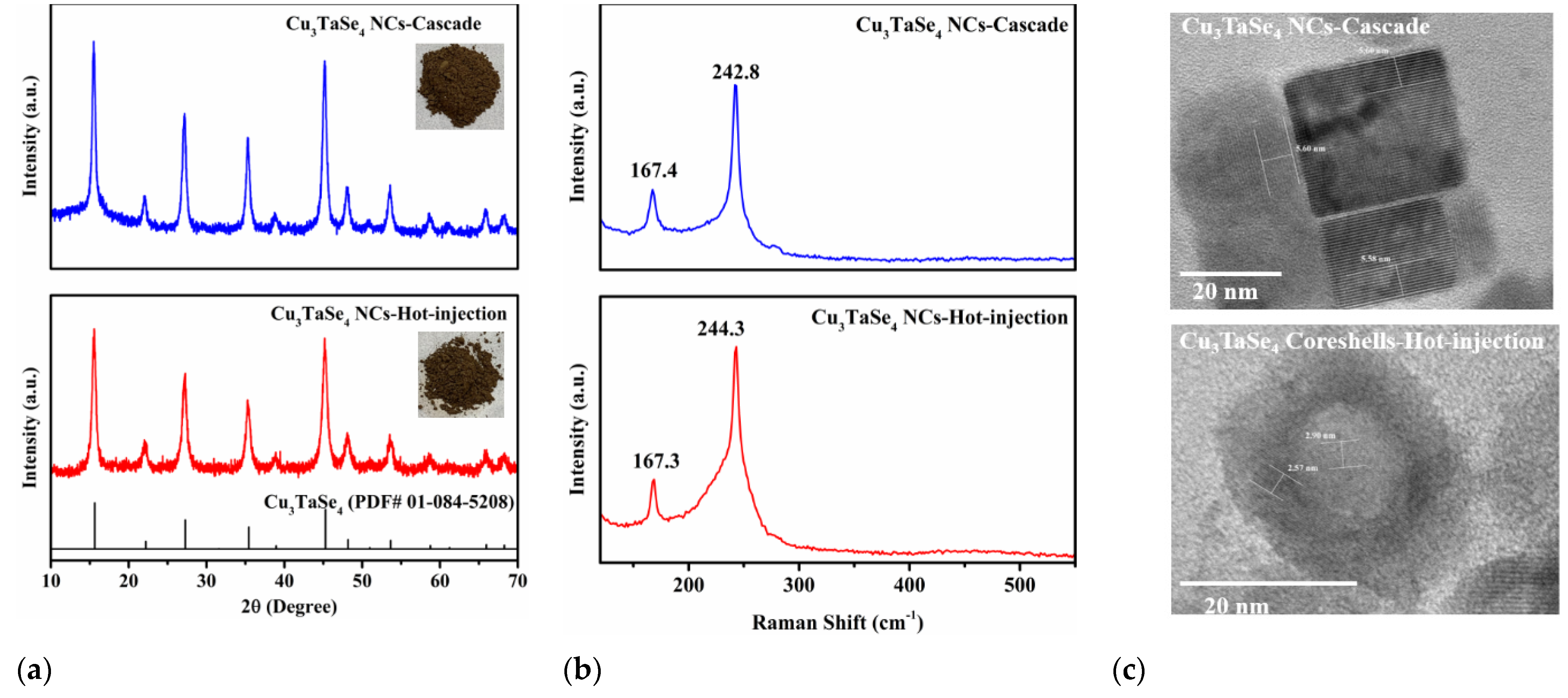
A comparison of XRD pattern for Cu3TaSe4 prepared by cascade and hot-injection method is shown in Figure 9a, where the characteristic peaks are the same and match to the cubic Cu3TaSe4 with a space group of P43m (215). Simultaneously, the Raman scattering peaks of both the cascade synthesized Cu3TaSe4 and the Cu3TaSe4 prepared by the hot-injection method locate at around 167.4 and 242.8 cm−1, as shown in Figure 9b, which are associated with F1b and A1 mode of Cu3TaSe4, respectively [30,41]. In the synthesis of Cu3TaSe4, when the Cu, Ta, and Se precursors are added with stoichiometric ratio, the obtained product showed both Cu7.16Se4 and Cu3TaSe4 phases, as shown in supporting information (Figure S3). As noted in the case of cascade synthesized Cu3TaS4 NCs, the synthesized Cu3TaS4 NCs did not maintain the 2D morphology of the TaS2 nanoflakes because that the incorporation of Cu cations caused additional stress which leads to tearing of the folded TaS2 nanoflakes into cubic nanocrystals. Similarly, the Cu3TaSe4 NCs prepared using the cascade method did not maintain the nanoflake morphology of TaSe2 template, but instead transformed into cubic shapes with irregular sizes, as shown in Figure 9c.
In contrast, the TEM image of the synthesized Cu3TaSe4 by hot-injection presents a core-shell morphology, where the interplanar spacing of 2.9 Å in the core region matches to the lattice (200) of cubic Cu3TaSe4, whereas the d-spacing of 2.57 Å located in the shell field could be attributed to the plane (210). Figure 10 displays the SEM-EDS of the synthesized Cu3TaSe4 using cascade synthesis, where Cu, Ta, and Se elements spread homogeneously in the synthesized Cu3TaSe4 materials. This suggest that core and shell have the same crystal structure, with different orientation. Further characterization is ongoing.
3.4.2. Mechanism for Cascade Synthesis of Cu3TaSe4 NCs
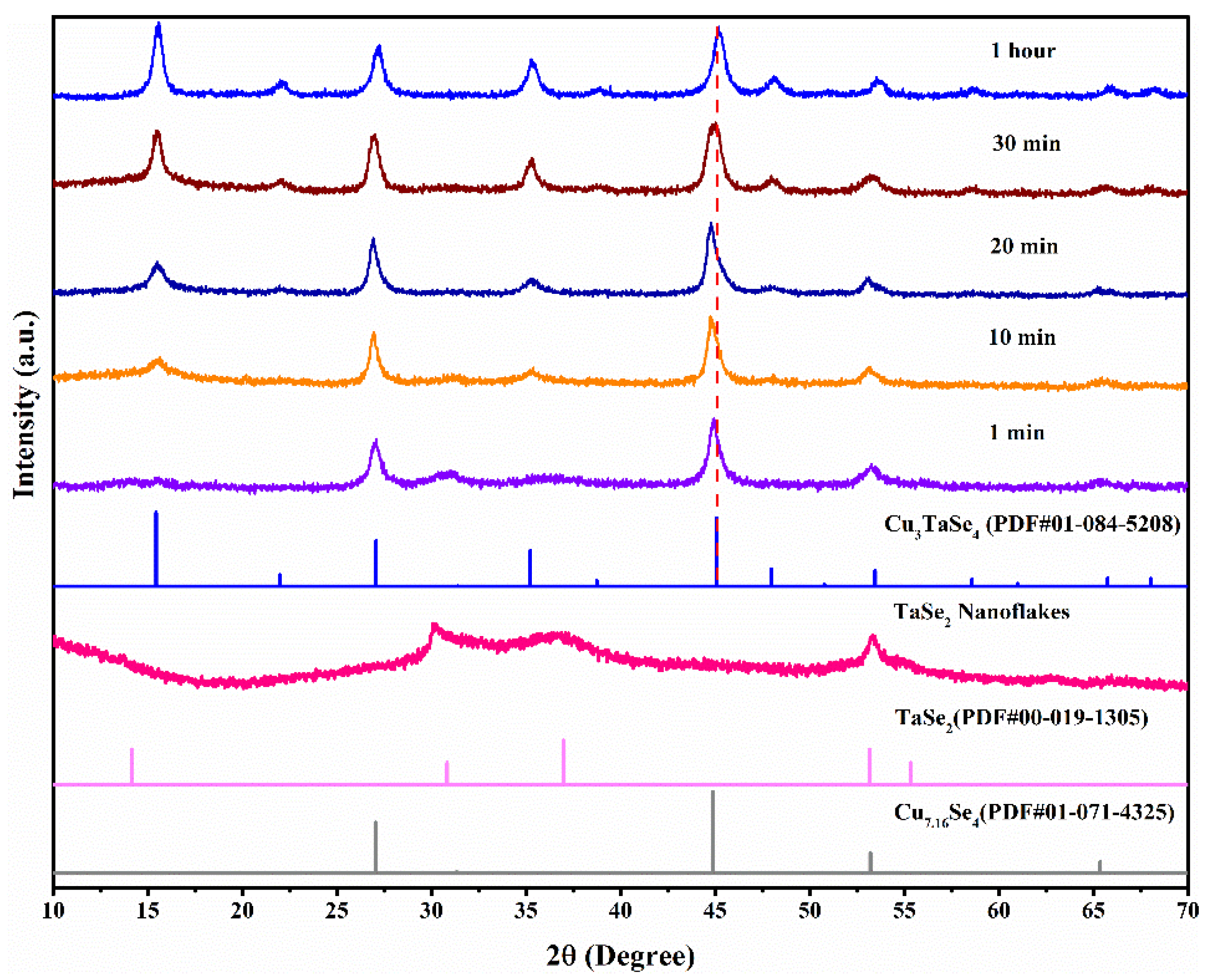
Phase structures of the products obtained at different times after injecting Cu cations were identified from XRD patterns shown in Figure 11. The suspension of formed TaSe2 nanoflakes in OLA-ODE was used as starting template. The characteristic peaks at 27.04°, 44.89°, and 53.2° 2θ that belong to the cubic Cu7.16Se4 were detected 1 min after injecting Cu2+ ions into the TaSe2 suspension. Meanwhile, trace amounts of TaSe2 residues could also be detected. When the reaction time was extended to 10 min, the characteristic Cu3TaSe4 peak at 15.64° started to appear, indicating the formation of Cu3TaSe4. However, it can be noted that the characteristic peaks of Cu7.16Se4 at 27.04°, 44.89°, and 53.2° are close to the dominant peaks of Cu3TaSe4 at 27.26°, 45.26°, and 53.65°, which makes it difficult to determine the purity of the products. Herein, we take the peak intensity ratio of the peak at 15.64° (100) to 45.26° (220) as the criteria to demonstrate the purity of the synthesized Cu3TaSe4, where the intensity ratio of (100) to (220) for the standard Cu3TaSe4 (PDF# 01-084-5208) is 1.08. Thus, when reacting for 10 min after injecting Cu cations, there were three phases in the reaction flask, including Cu7.16Se4, TaSe2, and Cu3TaSe4. When the reaction time was prolonged to 20 min, the TaSe2 phase disappeared, and a mixed phase of Cu7.16Se4 and Cu3TaSe4 were present in the reaction mixture at this stage. When the reaction proceeded for 1 h, the peak intensity ratio of (100) to (220) converted to approximately 1.09, implying that the pure Cu3TaSe4 was obtained. These XRD observations suggested that the incorporation of Cu cations triggered the rapid nucleation of Cu7.16Se4, and then the formed Cu7.16Se4 consumed the folded TaSe2 nanoflakes to form Cu3TaSe4 NCs. The overall color change of the reaction with reaction time is shown in Supporting Information (Figure S4a).
3.4.3. Mechanism for Hot-Injection Formation of Cu3TaSe4 NCs
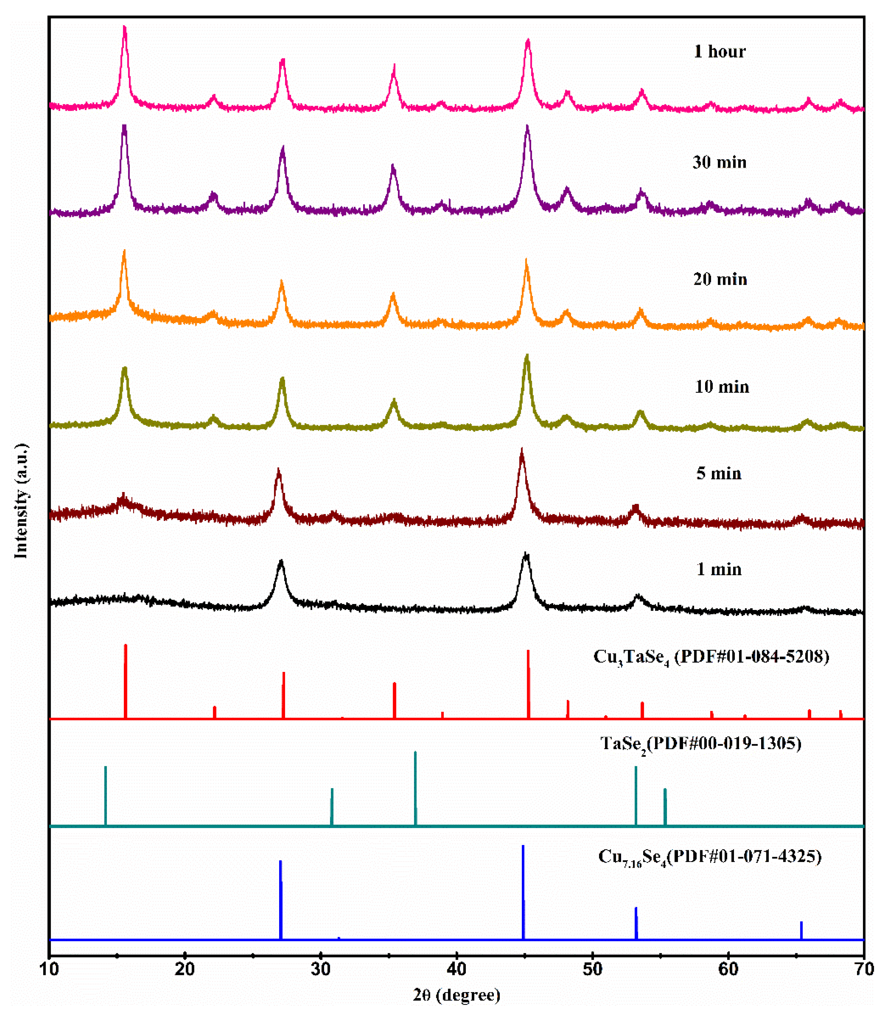
To assess the mechanism of Cu3TaSe4 NCs formation using the hot-injection method, we investigated the XRD patterns and color change of products at different reaction times, as shown in Figure 12 and Figure S4b, respectively. Once injecting the Cu-Ta precursor into the hot selenium solution, the first primary phase of Cu7.16Se4 was observed in the XRD patterns (Figure 12), indicating that the Cu7.16Se4 formed rapidly within 1 min, which was consistent with the cascade synthesis of Cu3TaSe4 NCs. After 5 min, the presence of the XRD peak at 15.64° highlights the formation of the cubic Cu3TaSe4 phase. As the reaction proceeded, the peak intensity ratio of the characteristic peak at 15.64° to 45.26 increased gradually, indicating the progressive conversion from Cu7.16Se4 to cubic Cu3TaSe4. Therefore, we hypothesize that the formation of Cu3TaSe4 NCs could follow the path below.
3.4.4. Optoelectrical and Conductivity Properties of Cu3TaSe4 NCs
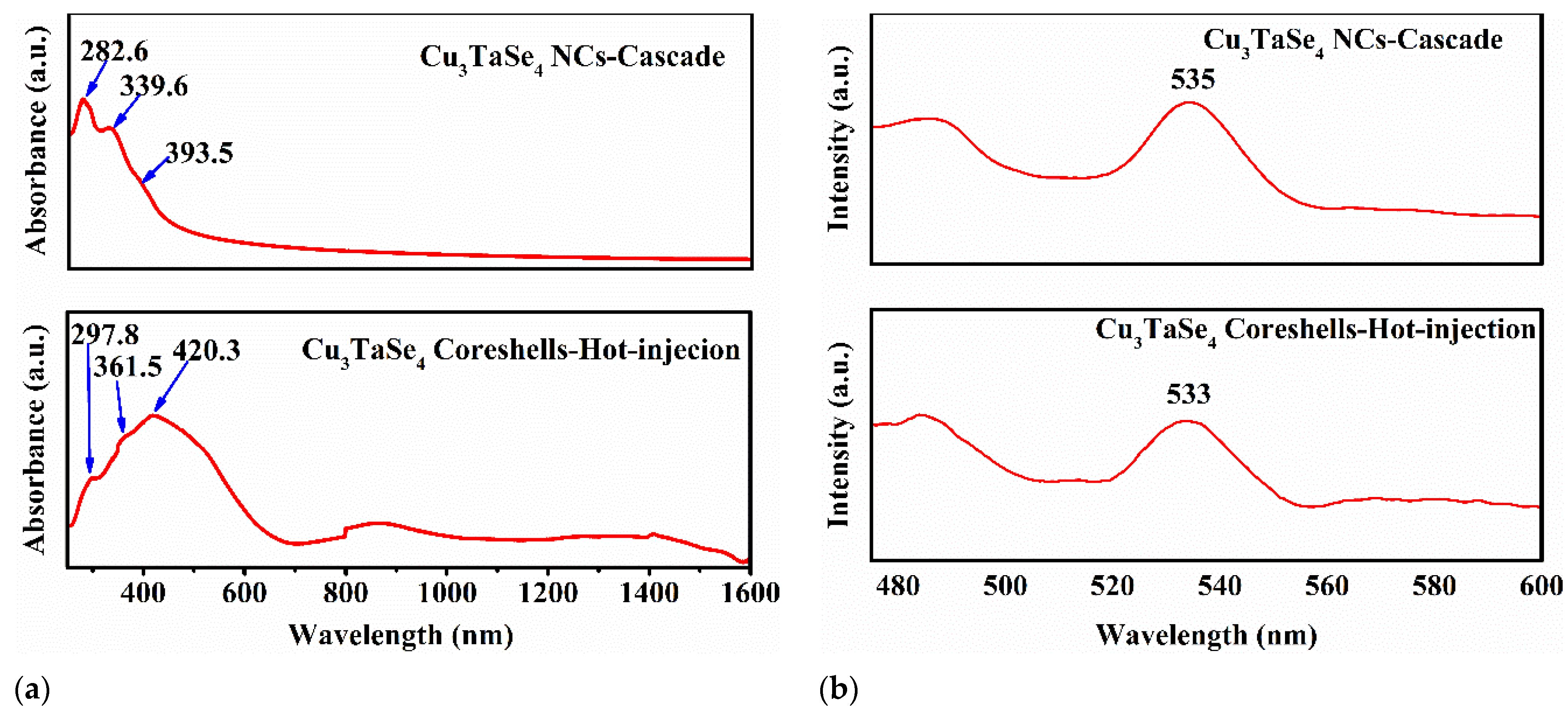
Optical spectra of synthesized Cu3TaSe4 NCs are shown in Figure 13a. The UV-Vis-NIR spectrum of the Cu3TaSe4 NCs prepared by the cascade method shows three primary peaks at around 282.6, 339.6, and 393.5 nm, respectively, whereas the spectrum of the Cu3TaSe4 core-shells exhibits a broad absorbing band at around 420.3 nm with two small characteristic peaks at 297.8 and 361.5 nm. Compared with the Cu3TaSe4 NCs, the UV-Vis-NIR spectrum of Cu3TaSe4 core-shells showed an additional absorption band at around 800-1000nm, which is related to the core-shell structured properties of Cu3TaSe4. Photoluminescence spectra of Cu3TaSe4 prepared by either the cascade method or hot-injection method (Figure 13b) showed a characteristic peak at around 535 nm, suggesting that the optical bandgap of Cu3TaSe4 was 2.32 eV, which is in good agreement with the previous reports [5,21,28,42].The I-V curve of fabricated Au/Cu3TaSe4 NCs-glass/Au device in Figure S5 shows a weak resistance. The electrical conductivity of Au/Cu3TaSe4 NCs-glass/Au device is very low compared to that of Cu3TaS4 NCs based device. Theoretically, the conductivity of semiconductor is proportional to the product of the mobility and the density of carriers. Herein, as p-type semiconductor, the majority carrier in Cu3TaS4 and Cu3TaSe4 semiconductors is the hole, thereby, their conductivity varies depending on the hole mobility and the density of holes. As described in the introduction, the calculated hole effective mass of Cu3TaS4 and Cu3TaSe4 are 0.944 and 0.831 mh*, Cu3TaSe4 has a lighter hole effective mass and should be more likely to display good p-type mobility. However, the defect concentration and the hole concentration could also affect the conductivity of devices. Speculating about the reason for a less conductivity of Au/Cu3TaSe4 NCs-glass/Au device, we could imagine that the fabricated devices would have a high defect density, which would trap the charge carriers or a low hole density of Cu3TaSe4 NCs. Further investigations in future studies are necessary to resolve the reason for the low conductivity, such as improving the thin-film quality.
Table 1 displays the morphology, size, and performance of the Cu3TaS4 and Cu3TaSe4 materials prepared under different experimental conditions. It is known from the table that the reaction temperature for preparing the Cu3TaS4 and Cu3TaSe4 materials by the solution-phase method is relatively lower than that of the solid-state method. Thereby, comparing the products prepared by the solid-state method and the solution-process, it is apparent that the solution-phase method is more controllable, facile, and time cost-effective.
4. Conclusions
We demonstrated and evaluated the methodology dependence of nanostructural geometries in the tantalum sulvanites. Using a cascade synthesis method, cubic green-yellow Cu3TaS4 NCs and brown Cu3TaSe4 NCs were successfully prepared. The hot-injection method leads to green Cu3TaS4 NCs and brown Cu3TaSe4 NC with core-shell nanostructure. XRD patterns analysis of the products prepared with different reaction times showed that Cu3TaS4 NCs could be formed in very short time (1 min) after the addition of Cu cations when using the cascade method, whereas the hot-injection method requires 30 min to form Cu3TaS4 NCs. During the formation of Cu3TaSe4 using the cascade method, the incorporation of Cu cations triggered rapid nucleation of Cu7.16Se4 and then the formed Cu7.16Se4 consumed the folded TaSe2 nanosheets to form Cu3TaSe4 NCs. While using the hot-injection method, the Cu3TaSe4 core-shells originated from Cu7.16Se4 seeds which rapidly formed within 1 min after adding the Cu-Ta precursors. The UV-Vis-NIR and photoluminescence measurements of the obtained Cu3TaS4 presented three characteristic absorbance peaks in the UV-Visible regions and unique emission peaks at 486.3 and 526.1nm. The green emission of Cu3TaS4 at 526.1 nm suggests the presence of a mid-band-gap charge trap caused by Cu vacancies near the valence band maximum. The absorption spectrum of Cu3TaSe4 NCs prepared by the cascade method shows three primary peaks at around 282.6, 339.6, and 393.5 nm. Surprisingly, the Cu3TaSe4 core-shells synthesized by the hot-injection method exhibit not only three primary peaks in the UV-Visible regions but also a unique absorption band at around 800–1000 nm; the phenomenon is currently investigated. Photoluminescence measurements of Cu3TaSe4 prepared by either cascade method or hot-injection shows an optical bandgap of 2.32 eV. In addition, the I-V curve of Au/Cu3TaS4 NCs-glass/Au device suggests the Cu3TaS4 NCs possess nonnegligible conductivity properties. The preliminary optoelectronic study show potential of Cu3TaS4 NCs as future transparent p-type conductors. Furthermore, the solution-based synthetic approaches of Cu3TaS4 NCs and Cu3TaSe4 NCs provide grounds for future applications of these promising semiconductors in the p-type TCM realm.
Supplementary Materials
The following are available online at https://0-www-mdpi-com.brum.beds.ac.uk/2073-4352/11/1/51/s1, Figure S1: XRD of Cu3TaS4 synthesized using stoichiometric ratio. Figure S2: Color changes for the cascade synthesis and hot-injection synthesis of Cu3TaS4 NCs, Figure S3: XRD of Cu3TaSe4 synthesized using stoichiometric ratio, Figure S4: Color changes for the cascade synthesis and hot-injection synthesis of Cu3TaSe4 NCs, Figure S5: I-V curve of the Au/Cu3TaSe4 NCs-glass/Au device.
Author Contributions
Formal analysis, M.L. and D.R.R.; data curation, M.L., C.-Y.C., C.-Y.L., and D.R.R.; writing—original draft preparation, M.L., C.-Y.L., and D.R.R.; writing—review and editing, D.R.R. and C.-Y.L.; supervision, D.R.R. and C.-Y.L.; project administration, D.R.R.; funding acquisition, D.R.R. and C.-Y.L. All authors have read and agreed to the published version of the manuscript.
Funding
80NSSC19M0201. ML was funded by NASA, award number 80NSSC19M0201.
Institutional Review Board Statement
Not applicable.
Informed Consent Statement
Not applicable.
Acknowledgments
The authors are very grateful to Zhiqun Lin and his group at Georgia Institute of Technology for access to PL instrumentation.
Conflicts of Interest
The authors declare no conflict of interest.
References
- Ginley, D.S.; Bright, C. Transparent Conducting Oxides. MRS Bull. 2000, 25, 15–18. [Google Scholar] [CrossRef]
- King, P.D.C.; Veal, T.D. Conductivity in transparent oxide semiconductors. J. Phys. Condens. Matter 2011, 23, 334214. [Google Scholar] [CrossRef]
- Granqvist, C.G. Transparent conductors as solar energy materials: A panoramic review. Sol. Energy Mater. Sol. Cells 2007, 91, 1529–1598. [Google Scholar] [CrossRef]
- Calnan, S.; Tiwari, A.N. High mobility transparent conducting oxides for thin film solar cells. Thin Solid Film. 2010, 518, 1839–1849. [Google Scholar] [CrossRef]
- Espinosa-García, W.F.; Pérez-Walton, S.; Osorio-Guillén, J.M.; Moyses Araujo, C. The electronic and optical properties of the sulvanite compounds: A many-body perturbation and time-dependent density functional theory study. J. Phys. Condens. Matter 2017, 30, 035502. [Google Scholar] [CrossRef] [PubMed]
- Gordon, R.G. Criteria for Choosing Transparent Conductors. MRS Bull. 2000, 25, 52–57. [Google Scholar] [CrossRef] [Green Version]
- Minami, T. Transparent conducting oxide semiconductors for transparent electrodes. Semicond. Sci. Technol. 2005, 20, S35–S44. [Google Scholar] [CrossRef]
- Hosono, H. Recent progress in transparent oxide semiconductors: Materials and device application. Thin Solid Film. 2007, 515, 6000–6014. [Google Scholar] [CrossRef]
- Ellmer, K. Past achievements and future challenges in the development of optically transparent electrodes. Nat. Photonics 2012, 6, 809–817. [Google Scholar] [CrossRef]
- Angela, N.F.; Monica, M.-M. Bridging the p-type transparent conductive materials gap: Synthesis approaches for disperse valence band materials. J. Photonics Energy 2020, 10, 1–17. [Google Scholar]
- Kawazoe, H.; Yanagi, H.; Ueda, K.; Hosono, H. Transparent p-Type Conducting Oxides: Design and Fabrication of p-n Heterojunctions. MRS Bull. 2000, 25, 28–36. [Google Scholar] [CrossRef] [Green Version]
- Park, C.H.; Zhang, S.B.; Wei, S.-H. Origin of p-type doping difficulty in ZnO: The impurity perspective. Phys. Rev. B 2002, 66, 073202. [Google Scholar] [CrossRef]
- Hosono, H.; Ueda, K. Transparent Conductive Oxides. In Springer Handbook of Electronic and Photonic Materials; Kasap, S., Capper, P., Eds.; Springer International Publishing: Cham, Switzerland, 2017; p. 1. [Google Scholar]
- Kawazoe, H.; Yasukawa, M.; Hyodo, H.; Kurita, M.; Yanagi, H.; Hosono, H. P-type electrical conduction in transparent thin films of CuAlO2. Nature 1997, 389, 939–942. [Google Scholar] [CrossRef]
- Nagarajan, R.; Draeseke, A.D.; Sleight, A.W.; Tate, J. p-type conductivity in CuCr1−xMgxO2 films and powders. J. Appl. Phys. 2001, 89, 8022–8025. [Google Scholar] [CrossRef]
- Farrell, L.; Norton, E.; Smith, C.M.; Caffrey, D.; Shvets, I.V.; Fleischer, K. Synthesis of nanocrystalline Cu deficient CuCrO2—A high figure of merit p-type transparent semiconductor. J. Mater. Chem. C 2016, 4, 126–134. [Google Scholar] [CrossRef] [Green Version]
- Dekkers, M.; Rijnders, G.; Blank, D.H.A. ZnIr2O4, a p-type transparent oxide semiconductor in the class of spinel zinc-d6-transition metal oxide. Appl. Phys. Lett. 2007, 90, 021903. [Google Scholar] [CrossRef]
- Hiramatsu, H.; Ueda, K.; Ohta, H.; Orita, M.; Hirano, M.; Hosono, H. Heteroepitaxial growth of a wide-gap p-type semiconductor, LaCuOS. Appl. Phys. Lett. 2002, 81, 598–600. [Google Scholar] [CrossRef]
- Ali, A.; Jahan, N.; Islam, A.K.M. Sulvanite Compounds Cu3TMS4 (TM= V, Nb and Ta): Elastic, Electronic, Optical and Thermal Properties using Firstprinciples Method. J. Sci. Res. 2014, 6, 407–419. [Google Scholar] [CrossRef] [Green Version]
- Ali, S.; van Smaalen, S. Single crystal X-ray structure of Cu3TaSe4 and a comparative study of Cu3MX4 (M = V, Nb, Ta; X = S, Se, Te). Z. Anorg. Allg. Chem. 2014, 640, 931–934. [Google Scholar] [CrossRef]
- Hersh, P.A. Wide Band Gap Semiconductors and Insulators: Synthesis, Processing and Characterization. Doctoral Dissertation, Oregon State University, Corvallis, OR, USA, 2007. [Google Scholar]
- Ikeda, S.; Aono, N.; Iwase, A.; Kobayashi, H.; Kudo, A. Cu3MS4 (M=V, Nb, Ta) and its Solid Solutions with Sulvanite Structure for Photocatalytic and Photoelectrochemical H2 Evolution under Visible-Light Irradiation. ChemSusChem 2019, 12, 1977–1983. [Google Scholar] [CrossRef]
- Bougherara, K.; Litimein, F.; Khenata, R.; Uçgun, E.; Ocak, H.Y.; Uğur, Ş.; Uğur, G.Ö.K.A.Y.; Reshak, A.H.; Soyalp, F.; Omran, S.B. Structural, Elastic, Electronic and Optical Properties of Cu3TMSe4 (TM = V, Nb and Ta) Sulvanite Compounds via First-Principles Calculations. Sci. Adv. Mater. 2012, 5, 97–106. [Google Scholar] [CrossRef] [Green Version]
- Li, Y.; Wu, M.; Zhang, T.; Qi, X.; Ming, G.; Wang, G.; Quan, X.; Yang, D. Natural sulvanite Cu3MX4 (M = Nb, Ta; X = S, Se): Promising visible-light photocatalysts for water splitting. Comput. Mater. Sci. 2019, 165, 137–143. [Google Scholar] [CrossRef]
- Kehoe, A.B.; Scanlon, D.O.; Watson, G.W. The electronic structure of sulvanite structured semiconductors Cu3MCh4 (M = V, Nb, Ta; Ch = S, Se, Te): Prospects for optoelectronic applications. J. Mater. Chem. C 2015, 3, 12236–12244. [Google Scholar] [CrossRef] [Green Version]
- Nitsche, R.; Wild, P. Crystal Growth and Electro-optic Effect of Copper-Tantalum-Selenide, Cu3TaSe4. J. Appl. Phys. 1967, 38, 5413–5414. [Google Scholar] [CrossRef]
- Petritis, D.; Martinez, G.; Levy-Clement, C.; Gorochov, O. Investigation of the vibronic properties of Cu3VS4, Cu3NbS4, and Cu3TaS4 compounds. Phys. Rev. B 1981, 23, 6773–6786. [Google Scholar] [CrossRef]
- Newhouse, P.F.; Hersh, P.A.; Zakutayev, A.; Richard, A.; Platt, H.A.S.; Keszler, D.A.; Tate, J. Thin film preparation and characterization of wide band gap Cu3TaQ4 (Q = S or Se) p-type semiconductors. Thin Solid Film. 2009, 517, 2473–2476. [Google Scholar] [CrossRef]
- Liu, M.; Lai, C.-Y.; Selopal, G.S.; Radu, D.R. Synthesis and optoelectronic properties of Cu3VSe4 nanocrystals. PLoS ONE 2020, 15, e0232184. [Google Scholar] [CrossRef]
- Schmidt, K.H.; Müller, A.; Bouwma, J.; Jellinek, F. Übergangsmetall-chalklogen-verbindungen IR-und raman-spektren von Cu3Mx4 (m = v, nb, ta; x = s, se). J. Mol. Struct. 1972, 11, 275–282. [Google Scholar] [CrossRef]
- Liu, M.; Lai, C.-Y.; Zhang, M.; Radu, D.R. Cascade synthesis and optoelectronic applications of intermediate bandgap Cu3VSe4 nanosheets. Sci. Rep. 2020, 10, 21679. [Google Scholar] [CrossRef]
- Sarkar, S.; Leach, A.D.P.; Macdonald, J.E. Folded Nanosheets: A New Mechanism for Nanodisk Formation. Chem. Mater. 2016, 28, 4324–4330. [Google Scholar] [CrossRef]
- Barbir, F. Chapter Four-Main Cell Components, Material Properties, and Processes. In PEM Fuel Cells, 2nd ed.; Barbir, F., Ed.; Academic Press: Boston, MA, USA, 2013; pp. 73–117. [Google Scholar]
- Sha, W.; Wu, X.; Keong, K.G. 8-Electrical resistivity of electroless copper deposit. In Electroless Copper and Nickel–Phosphorus Plating; Sha, W., Wu, X., Keong, K.G., Eds.; Woodhead Publishing: Cambridge, UK, 2011; pp. 117–134. [Google Scholar]
- Hassanien, A.S.; Akl, A.A. Electrical transport properties and Mott’s parameters of chalcogenide cadmium sulphoselenide bulk glasses. J. Non Cryst. Solids 2016, 432, 471–479. [Google Scholar] [CrossRef]
- Hassanien, A.S.; Akl, A.A. Effect of Se addition on optical and electrical properties of chalcogenide CdSSe thin films. Superlattices Microstruct. 2016, 89, 153–169. [Google Scholar] [CrossRef]
- Santos, T.G. 5-Characterization of FSP by electrical conductivity. In Surface Modification by Solid State Processing; Miranda, R., Ed.; Woodhead Publishing: Cambridge, UK, 2014; pp. 153–176. [Google Scholar]
- Singh, Y. Electrical Resistivity Measurements: A review. Int. J. Mod. Phys. Conf. Ser. 2013, 22, 745–756. [Google Scholar] [CrossRef]
- Ehrstein, J.R. Two-Probe (Spreading Resistance) Measurements for Evaluation of Semiconductor Materials and Devices. In Nondestructive Evaluation of Semiconductor Materials and Devices; Zemel, J.N., Ed.; Springer: Boston, MA, USA, 1979; pp. 1–66. [Google Scholar]
- Jeong, S.; Yoo, D.; Jang, J.-T.; Kim, M.; Cheon, J. Well-Defined Colloidal 2-D Layered Transition-Metal Chalcogenide Nanocrystals via Generalized Synthetic Protocols. J. Am. Chem. Soc. 2012, 134, 18233–18236. [Google Scholar] [CrossRef] [PubMed]
- Grima-Gallardo, P.; Salas, M.; Contreras, O.; Power, C.; Quintero, M.; Cabrera, H.; Zumeta-Dubé, I.; Rodríguez, A.; Aitken, J.; Brämer-Escamilla, W. Cu3TaSe4 and Cu3NbSe4: X-ray diffraction, differential thermal analysis, optical absorption and Raman scattering. J. Alloy. Compd. 2016, 658, 749–756. [Google Scholar] [CrossRef]
- Espinosa-García, W.F.; Valencia-Balvín, C.; Osorio-Guillén, J.M. Phononic and thermodynamic properties of the sulvanite compounds: A first-principles study. Comput. Mater. Sci. 2016, 113, 275–279. [Google Scholar] [CrossRef]
Figure 1.
Characterization of the synthesized TaS2 nanoflakes. (a) XRD pattern. (b) Crystal structure. (c) TEM image.
Figure 1.
Characterization of the synthesized TaS2 nanoflakes. (a) XRD pattern. (b) Crystal structure. (c) TEM image.

Figure 2.
Characterization of Cu3TaS4 NCs prepared by cascade and hot-injection method. (a) XRD pattern. (b) Raman spectra. (c) TEM images.
Figure 2.
Characterization of Cu3TaS4 NCs prepared by cascade and hot-injection method. (a) XRD pattern. (b) Raman spectra. (c) TEM images.

Figure 3.
SEM-EDS mapping of Cu3TaS4 NCs by cascade method.

Figure 4.
Mechanism for cascade synthesis of Cu3TaS4 NCs.

Figure 5.
Mechanism for hot-injection synthesis of Cu3TaS4 NCs.

Figure 6.
(a) UV-Vis-NIR absorption spectrum. (b) PL spectrum of the synthesized Cu3TaS4 NCs in ethanol.
Figure 6.
(a) UV-Vis-NIR absorption spectrum. (b) PL spectrum of the synthesized Cu3TaS4 NCs in ethanol.

Figure 7.
(a) Schematics of the device configuration for the I-V measurement. (b) I-V curve of the Au/Cu3TaS4 NCs-glass/Au device and Au/Glass/Au.
Figure 7.
(a) Schematics of the device configuration for the I-V measurement. (b) I-V curve of the Au/Cu3TaS4 NCs-glass/Au device and Au/Glass/Au.

Figure 8.
Characterization of synthesized TaSe2 nanoflakes. (a) XRD pattern. (b) Crystal structure. (c) TEM image.
Figure 8.
Characterization of synthesized TaSe2 nanoflakes. (a) XRD pattern. (b) Crystal structure. (c) TEM image.

Figure 9.
Characterization of Cu3TaSe4 prepared by cascade and hot-injection methods. (a) XRD pattern. (b) Raman spectra. (c) TEM images.
Figure 9.
Characterization of Cu3TaSe4 prepared by cascade and hot-injection methods. (a) XRD pattern. (b) Raman spectra. (c) TEM images.

Figure 10.
SEM-EDS mapping of Cu3TaSe4 NCs synthesized by cascade method.

Figure 11.
Mechanism for cascade synthesis of Cu3TaSe4 NCs.

Figure 12.
Mechanism for hot-injection of Cu3TaSe4 NCs.

Figure 13.
(a) UV-Vis-NIR absorption spectra of Cu3TaSe4 NCs and Cu3TaSe4 Core-shells. (b) PL spectra of Cu3TaSe4 NCs and Cu3TaSe4 Core-shells.
Figure 13.
(a) UV-Vis-NIR absorption spectra of Cu3TaSe4 NCs and Cu3TaSe4 Core-shells. (b) PL spectra of Cu3TaSe4 NCs and Cu3TaSe4 Core-shells.


Table 1.
Experimental conditions and performance of Cu3TaS4 and Cu3TaSe4 nanomaterials synthesized with different methods.
Table 1.
Experimental conditions and performance of Cu3TaS4 and Cu3TaSe4 nanomaterials synthesized with different methods.
| Compound | Synthesis Method | Formation Condition | Shape and Dimension | Performance | |
|---|---|---|---|---|---|
| Color | Conductivity | ||||
| Cu3TaS4 | Solid-state Method [21,26] | 800 °C for 48 h | - | light brown | - |
| Cascade | TaS2, 300 °C for 2 h Cu3TaS4, 300°C for 1h | Cubic, ~20 nm | mustard-green | 1.38 × 10⁻⁹ S·m−1 | |
| Hot injection | 300 °C for 1 h | Cubic, ~15 nm | yellow | ||
| Cu3TaSe4 | Solid-state Method [20] | Polycrystalline Powder 880 for 98 h Single crystals 890 for 143 h | Cubic | Orange yellow | - |
| Cascade | TaSe2, 305 °C for 1 h Cu3TaSe4, 305 °C for 1h | Cubic, irregular sizes | brown | weak resistance | |
| Hot injection | 300 °C for 1 h | Core-shell, ~25 nm | brown | - | |
Publisher’s Note: MDPI stays neutral with regard to jurisdictional claims in published maps and institutional affiliations. |
© 2021 by the authors. Licensee MDPI, Basel, Switzerland. This article is an open access article distributed under the terms and conditions of the Creative Commons Attribution (CC BY) license (http://creativecommons.org/licenses/by/4.0/).
Share and Cite
MDPI and ACS Style
Liu, M.; Lai, C.-Y.; Chang, C.-Y.; Radu, D.R. Solution-Based Synthesis of Sulvanite Cu3TaS4 and Cu3TaSe4 Nanocrystals. Crystals 2021, 11, 51. https://0-doi-org.brum.beds.ac.uk/10.3390/cryst11010051
AMA Style
Liu M, Lai C-Y, Chang C-Y, Radu DR. Solution-Based Synthesis of Sulvanite Cu3TaS4 and Cu3TaSe4 Nanocrystals. Crystals. 2021; 11(1):51. https://0-doi-org.brum.beds.ac.uk/10.3390/cryst11010051
Chicago/Turabian StyleLiu, Mimi, Cheng-Yu Lai, Chen-Yu Chang, and Daniela R. Radu. 2021. "Solution-Based Synthesis of Sulvanite Cu3TaS4 and Cu3TaSe4 Nanocrystals" Crystals 11, no. 1: 51. https://0-doi-org.brum.beds.ac.uk/10.3390/cryst11010051
Note that from the first issue of 2016, this journal uses article numbers instead of page numbers. See further details here.