
A Study of Interfacial Electronic Structure at the CuPc/CsPbI2Br Interface
by
 ,
,
Zengguang Tang
1,2,3 ,
,
Liujiang Zhang
1,2,3,
Zhenhuang Su
1,2,3,
Zhen Wang
1,2,3,
Li Chen
1,2,
Chenyue Wang
1,2,
Guoping Xiao
1 and
Xingyu Gao
1,2,* 1
Shanghai Institute of Applied Physics, Chinese Academy of Sciences, Shanghai 201800, China
2
Shanghai Synchrotron Radiation Facility, Shanghai Advanced Research Institute, Chinese Academy of Sciences, Shanghai 201210, China
3
University of Chinese Academy of Sciences, Beijing 100049, China
*
Author to whom correspondence should be addressed.
Crystals 2021, 11(5), 547; https://0-doi-org.brum.beds.ac.uk/10.3390/cryst11050547
Submission received: 14 April 2021
/
Revised: 2 May 2021
/
Accepted: 10 May 2021
/
Published: 14 May 2021
Abstract
:In this article, CsPbI2Br perovskite thin films were spin-coated on FTO, on which CuPc was deposited by thermal evaporation. The electronic structure at the CsPbI2Br/CuPc interface was examined during the CuPc deposition by in situ X-ray photoelectron spectroscopy (XPS) and ultraviolet photoelectron spectroscopy (UPS) measurements. No downward band bending was resolved at the CsPbI2Br side, whereas there is ~0.23 eV upward band bending as well as a dipole of ~0.08 eV identified at the molecular side. Although the hole injection barrier as indicated by the energy gap from CsPbI2Br valance band maximum (VBM) to CuPc highest occupied molecular orbital (HOMO) was estimated to be ~0.26 eV, favoring hole extraction from CsPbI2Br to CuPc, the electron blocking barrier of ~0.04 eV as indicated by the offset between CsPbI2Br conduction band minimum (CBM) and CuPc lowest unoccupied molecular orbital (LUMO) is too small to efficiently block electron transfer. Therefore, the present experimental study implies that CuPc may not be a promising hole transport material for high-performance solar cells using CsPbI2Br as active layer.
1. Introduction
Organic–inorganic hybrid perovskite solar cells (PSCs) have been developed rapidly in the past ten years. To be specific, their power conversion efficiency (PCE) already jumped from initial 3.8% to the certified 25.2% up to now [1,2]. The success of PSCs takes advantages of many merits of perovskites, such as broad and strong light absorption, low exciton binding energy, impressive high charge carrier mobility, long free carrier diffusion length along with their low-cost and flexible fabricating processes [3], hence attracting widespread interest among the photovoltaic community.
Thus far, all high-performance PSCs with PCEs of over 20% were based on organic–inorganic hybrid perovskites [4]. However, there are several drawbacks that hinder the commercialization of these PSCs, including their toxicity, poor long-term and thermal stability. Organic–inorganic hybrid perovskites consist of organic cations, including methylammonium (MA) or formamidinium (FA), in a lead halide framework [5]. To avoid the toxicity brought by the presence of Pb2+ in PSCs, there have been many research works dedicated to Pb-free perovskites [6,7,8,9]. Their thermal instability is usually associated with the decomposition of the perovskite films caused by the volatilization of the organic cations under high temperatures (exceeding 200 °C) [10,11]. It is known that thin films blended of organic formamidinium and inorganic cesium (Cs) cations made the perovskite structure stable at temperatures over 100 °C [12]. Furthermore, the organic cations were replaced totally by inorganic cations maintaining the crystal structure; for example, APbX3 (A = Rb, Cs; X = I, Br and Cl) exhibits superior thermal compositional stability with the initial PCE of resultant PSCs even at temperatures up to 400 °C [13,14]. Therefore, the black phase of CsPbI3 has an ideal band gap (Eg = 1.73 eV), which is a suitable choice for photovoltaic devices with the potential for achieving the highest PCE among cesium lead halide perovskites (CsPbI(3−X)Brx). Unfortunately, CsPbI3 is metastable, which turns into yellow orthorhombic phase (non-perovskite structure) at room temperature under ambient conditions within a few minutes [15]. In comparison with CsPbI3, CsPbBr3 presents improved long-term and moisture stability, which can be explained by Goldschmidt tolerance factor which was increased due to the replacement of I− by smaller Br− [16]. However, CsPbBr3 has a band gap as large as 2.25 eV, which limits the achievable PCE of its PSCs considering the Shockley–Queisser limit [15,17]. On the other hand, CsPbI2Br as a mixed-halide perovskite with an ideal band gap of 1.92 eV exhibits both phase stability and promising performance at high temperatures or under humidity conditions, and its theoretical PCE is up to ~21% [18]. Nevertheless, the best PCE achieved is significantly lower than the theoretical predication [19,20].
To promote device performance of CsPbI2Br, many approaches have been developed, including doping engineering and surface engineering of the active layer [21,22]. However, there has been no report about the interfacial electronic structure between the CsPbI2Br layer and the charge transport layers, which is also vital for the PSC performance. For instance, PSCs with ZnO as the electron transport layer (ETL) exhibit better performance than TiO2, not only because of their good optoelectronic properties, but also their more appropriate work function (WF) [23,24,25,26,27]. Photoemission techniques have been widely used to find out the interfacial electronic structure in the search for suitable hole transport layer (HTL) or ETL materials in PSCs. In the meantime, the phthalocyanine family of molecules provides wide choices for energy level modifications in solar cells [28]. As an example, copper phthalocyanine (CuPc) is an extensively used molecule for applications in organic optoelectronic devices and even organic field effect transistors due to its strong absorption, long exciton diffusion length and outstanding stability [29,30,31,32]. Herein, we will evaluate the viability of CuPc as an HTL material for CsPbI2Br-based PSCs by investigating the energy level alignment using in situ X-ray photoelectron spectroscopy (XPS) and ultraviolet photoelectron spectroscopy (UPS). The observed interfacial electronic structure favors hole injection but cannot efficiently block the electron transfer, which suggests that CuPc may not be a potential HTL material for high-performance all-inorganic CsPbI2Br solar cells.
2. Materials and Methods
FTO glass substrates were washed sequentially using ethanol, detergent, acetone, de-ionized water and ethanol, then dried in N2 flow and treated in UV-ozone for 15 min. The SnO2 solution (VSnO2:VH2O = 1:5) was spin-casted upon FTO at 4000 rpm for 30 s, followed by heating at 150 °C for 30 min and UV-ozone treatment for 15 min. The CsPbI2Br thin films were deposited using a one-step approach in a glove box as reported in the literature [33]. To make perovskite precursor solution, 120 mg cesium iodide (CsI, 99.99%), 106 mg lead iodide (PbI2, 99.99%) and 85 mg lead bromide (PbBr2, 99.99%) powder, all bought from Xi’an Polymer Light Technology Corp, Xi’an, China were dissolved in 800 μL N,N-dimethylformamide (DMF, 99.9%, bought from Shanghai Aladdin Bio-Chem Technology Co.,LTD, Shanghai, China) solution and then 120 μL dimethyl sulfoxide (DMSO, 99.9%, purchased from Shanghai Aladdin Bio-Chem Technology Co.,LTD, Shanghai, China) were added. Afterwards, the prepared precursor solution was maintained at 60 °C on a hot plate overnight. When the precursor solution was cooled down to room temperature, it was spin-coated upon SnO2 substrate at 3500 rpm for 30 s, with anti-solvent chlorobenzene dropped onto the spinning film after 10 s of spinning. Finally, gradient annealing at 150 °C for 2 min, 250 °C for 3 min and then 350 °C for 5 min was applied to complete the fabrication of CsPbI2Br films.
The CuPc film was prepared by the vapor deposition method, instead of the solution process approach, which not only minimizes the influence of external carbon contamination, but also enables the preparation of angstrom-thick film. The photoelectron spectroscopy measurements were performed in situ after the deposition of CuPc in an ultrahigh vacuum (UHV) system with a base pressure of ~4 × 10⁻¹⁰ mbar. To minimize the decomposition of the perovskite film, the as-prepared CsPbI2Br films are transferred from the glove box (under N2 environment) to the preparation chamber of the photoemission UHV system within ~8 min. The photoelectrons of XPS and UPS were excited by a monochromatic Al-Kα (hν = 1486.6 eV) lab source and a Helium lamp (He I: hν = 21.2 eV), respectively. Photoemission spectra were taken at normal emission by a PHOIBOS 100 analyzer, the overall instrumental energy resolution for XPS and UPS are 0.45 eV and 15 meV, respectively. CuPc powder bought from Sigma-Aldrich was put in a quartz crucible heated electrically for evaporation. The source temperature was heated to ~350 °C during evaporation and the vacuum was lower than 10−8 mbar. The CuPc film thickness and deposition rate were calculated by comparing the Pb 4f7/2 XPS signal from the substrate during the film growth with that from the bare CsPbI2Br substrate. The XPS spectra were fitted by using the XPSPEAK 4.1 software.
Grazing incidence X-ray diffraction (GIXRD) was done at the BL14B1 beamline of Shanghai Synchrotron Radiation Facility (SSRF) and the applied photon energy of X-ray was 10 keV. The 2-dimensional GIXRD images were taken by using a MarCCD 225 detector vertically placed along the X-ray path away from the samples. The sample–detector distance was calibrated from the analysis of the GIXRD pattern from a lanthanum hexaboride sample by using FIT2D. A Zeiss GeminiSEM 300 system was used to measure high resolution field emission scanning electron microscopy (FESEM) with up to 2 × 10⁶ magnification to investigate the film surface morphology.
3. Results and Discussion
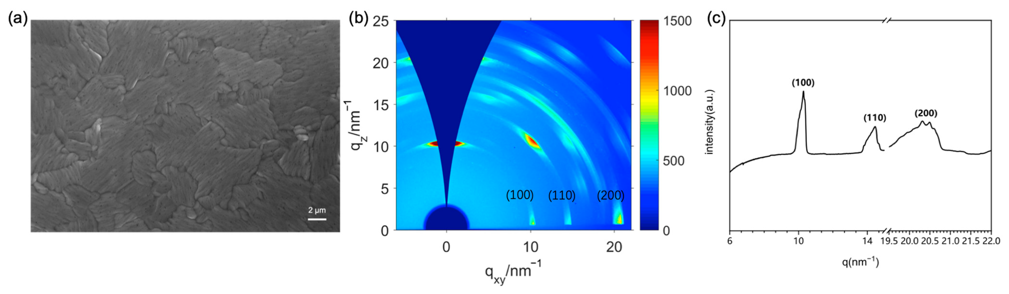
As shown in Figure 1a, the top-view SEM image of a fabricated CsPbI2Br film reveals a densely packed smooth surface without pin-holes, indicating the high quality of the film. To further verify the film quality, the GIXRD pattern from a CsPbI2Br film and its derived 1D-GIXRD are shown in Figure 1b,c, respectively. There are intense diffraction streaks along the diffraction rings for perovskite in Figure 1b, indicating the formation of highly crystallized film with strong preferential orientations. The three characteristic diffraction peaks in Figure 1c at scattering vectors (q = 4πsin θ/λ) q ≈ 10 nm−1, q ≈ 14.5 nm−1 and q ≈ 20.3 nm−1 correspond to the (100), (110) and (200) crystal planes of α-phase (cubic phase) perovskite, respectively, which is in line with previous reports [34]. The present GIXRD pattern is a little different from the cubic CsPbI3 perovskite phase, owing to the presence of bromide content. No diffraction peaks associated with PbI2 (q ≈ 9.0 nm−1), PbBr2 (q ≈ 9.1 nm−1) and δ-phase (orthorhombic phase, q ≈ 7.1 nm−1) CsPbI2Br can be seen in Figure 1c, indicating a complete phase transition from the perovskite precursor to α-phase CsPbI2Br [35]. It is worth noting that there are bright streaks at (100) and (110) diffraction rings in Figure 1b, indicating preferential orientations of the perovskite crystalline.
In the XPS survey spectrum of the pristine CsPbI2Br film (cf. Appendix A Figure A1), oxygen and adventitious carbon signals (around 530 eV and 285 eV, respectively) in the pristine perovskite are barely observable, demonstrating minimized surface contamination. It is also noticed that no Sn signal (Sn 3d5/2 at ~485 eV) can be detected, attesting that the high temperature of up to 350 °C used for annealing did not lead to the upward diffusion of SnO2.
To investigate the electronic structure at the CuPc/CsPbI2Br interface, XPS measurements were conducted and the core level spectra of the elements from CsPbI2Br film with different CuPc thicknesses are reported in Figure 2a–d. The binding energies of Cs 3d5/2, Pb 4f7/2, I 3d5/2 and Br 3d5/2 peaks for pristine CsPbI2Br film are located at 724.99 eV, 138.61 eV, 619.41 eV and 68.74 eV, respectively. Upon the deposition of CuPc films, the binding energy of all these characteristic features remains almost constant within an uncertainty of less than 0.05 eV, as shown in their corresponding figure as well as their evolutions with increasing CuPc thickness summarized in Figure 2e, which indicates no band bending at this side of the CuPc/CsPbI2Br interface.
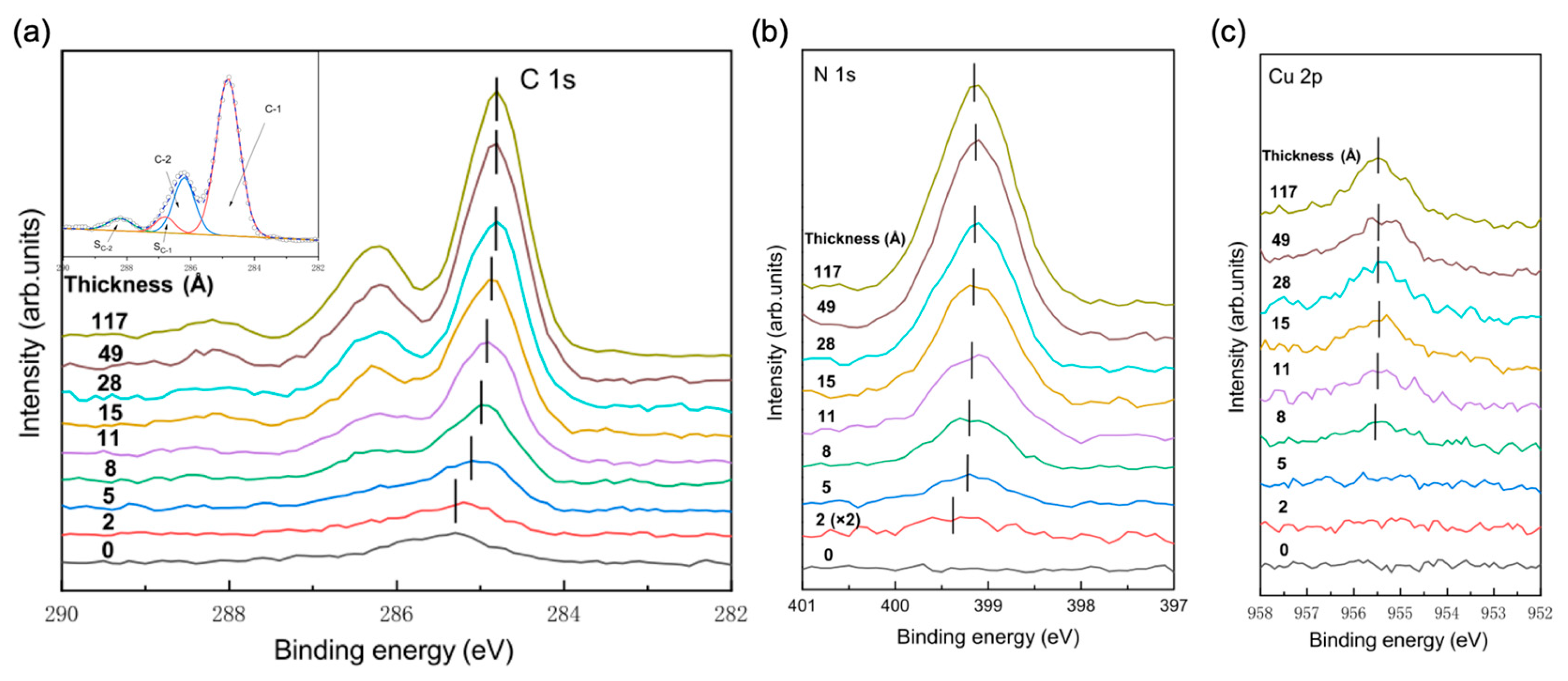
Figure 3 shows the evolutions of C 1s, N 1s and Cu 2p for the CuPc film as functions of film thicknesses. In C 1s spectra (cf. Figure 3a), the peak at 285.5 eV for the pristine CsPbI2Br film is assigned to adventitious carbon [36]. Features corresponding to CuPc appear and become dominant after 5 Å deposition. The inset shows the fitting curve for C 1s spectrum at a CuPc thickness of 117 Å. The C-1 (284.8 eV) and C-2 (286.2 eV) are assigned to aromatic carbon of the benzene rings and pyrrole carbon linked to nitrogen, respectively, with corresponding shake-up features located at higher binding energy of 286.8 eV and 288.2 eV, which agrees well with previous reports [37,38,39]. No additional features in C 1s spectra are observed, suggesting no chemical bonds formed between CuPc and CsPbI2Br. The peak positions of C-1 feature are guided by solid bars in Figure 3a, which shift to lower binding energy continuously by ~0.23 eV from 2 Å to 117 Å. The thickness-dependent N 1s and Cu 2p spectra are shown in Figure 3b,c, respectively. It is noticed that N 1s peaks shift almost identically to the lower binding energy side by ~0.23 eV. Although Cu 2p cannot be resolved below 5 Å due to the very low atomic concentration of Cu, it also shifts with increasing thicknesses to lower binding energy. The local shift of all core levels in the same fashion is the characteristic for the band bending [40,41]. In summary, all the photoemission peaks from the CuPc shift towards lower binding energy continuously during evaporation, pointing to an upward band bending at the CuPc side of the CsPbI2Br/CuPc interface.
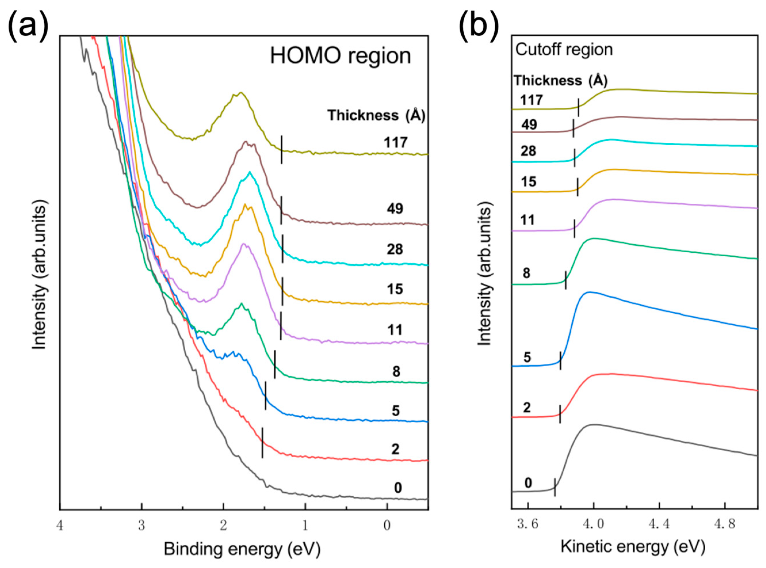
The UPS spectra can be used additionally to explore the possible chemical interaction and band bending at the CuPc/CsPbI2Br interface. Figure 4 illustrates the changes of VB spectra and the secondary electron cut-off (SECO) with increasing CuPc thickness on CsPbI2Br. As shown in Figure 4a, the VBM of the pristine CsPbI2Br occurs at 1.78 eV, and HOMO onset of CuPc molecule is found at ~1.52 eV after 2 Å deposition. The HOMO onset gradually shifts to lower binding energy by ∼0.23 eV, consistent with the core level results. No additional VB features are observed, confirming weak CuPc–CsPbI2Br interactions. In Figure 4b, the WF of the pristine CsPbI2Br film is determined to be ∼3.76 eV. It increases gradually to 3.91 eV at 15 Å and remains almost unchanged for further CuPc deposition.
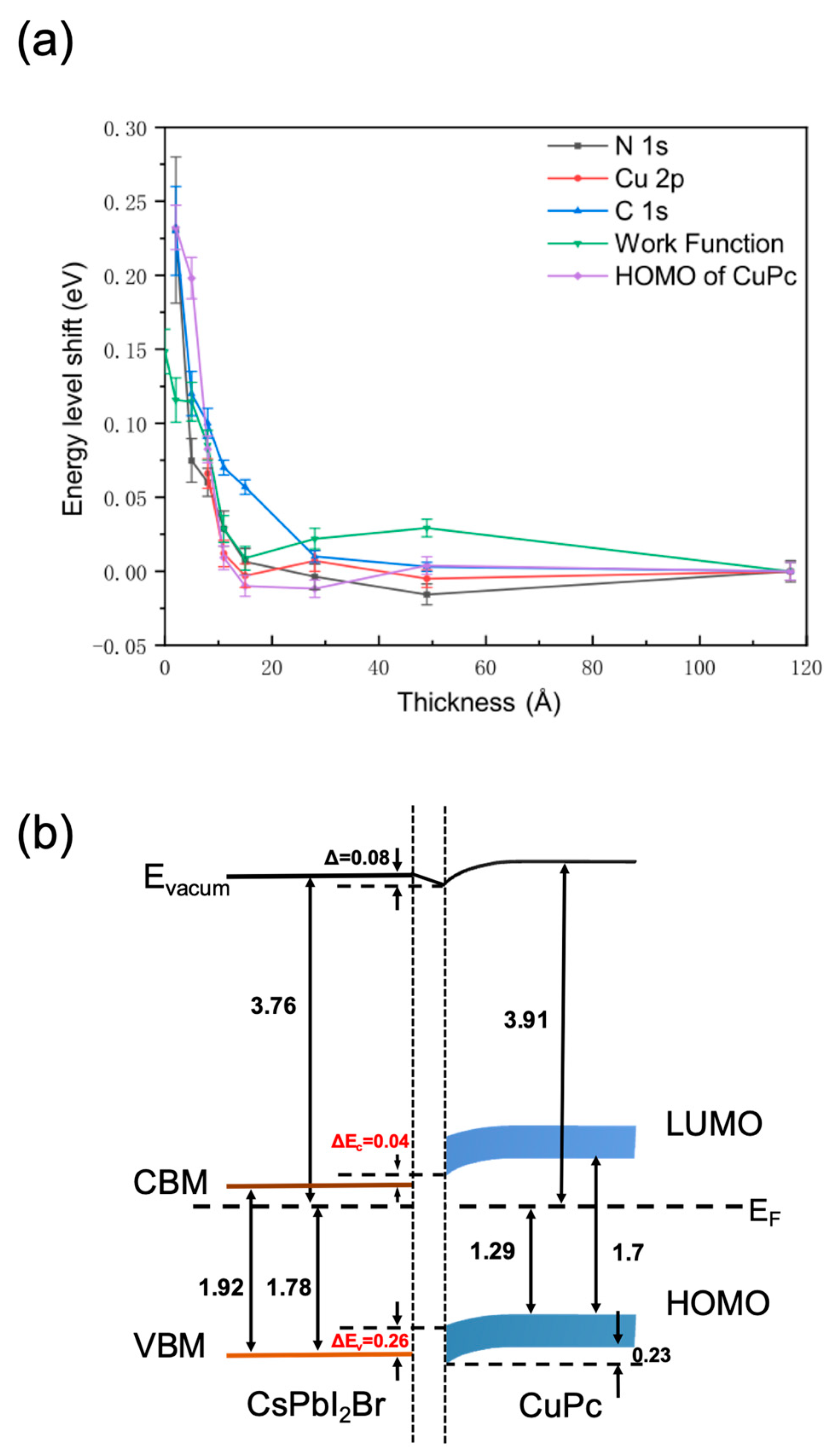
Figure 5a summarizes the evolutions of core-levels, HOMO onset of CuPc and WF as functions of film thickness. It is clear that core-levels and HOMO onset shift almost in the same way to lower binding by ~0.23 eV, conforming the ‘band bending’ like shift at CuPc side. The band bending is also verified by the shift of WF to lower binding energy, but only by ~0.15 eV, which indicates the formation of dipole of ~0.08 eV at the side of the CuPc. The energy level diagram at the CuPc/CsPbI2Br interface is depicted in Figure 5b. It should be noticed that the uncertainty of this energy diagram is estimated to be ~0.05 eV. For bare CsPbI2Br substrate, the VBM is found at ~1.78 eV below the Fermi level, which places the conduction band minimum (CBM) ~0.14 eV above the Fermi level considering a band gap of 1.92 eV [42], indicating the heavily n-type nature of as-prepared CsPbI2Br film. To achieve thermodynamic equilibrium, electrons are accumulated at the CuPc side, leading to an upward band bending as well as a dipole of ~0.08 eV [40,41]. Considering the band gap of 1.7 eV and HOMO onset ~1.52 eV at CuPc/CsPbI2Br interface [30], the LUMO is placed at ~0.18 eV above Fermi level. A ~0.23 eV ‘band bending’ like shift occurs at the CuPc side due to the electron accumulation until the thermodynamics equilibrium is reached. The hole injection barrier at the CuPc/CsPbI2Br interface, as indicated by the difference between CsPbI2Br VBM and CuPc HOMO, is ~0.26 eV, which is comparable with that of 0.4–0.5 eV found at the extensively studied Spiro–OMeTAD/CH3NH3PbI3 interface and facilitate holes injection/transfer from perovskite into the CuPc [43]. On the other hand, the electron blocking barrier (ΔEc), which is the energy offset between CsPbI2Br CBM and CuPc LUMO, is determined to be ~0.04 eV at the interface, which would be too small to prevent photogenerated electrons from flowing into the CuPc layer. Although there are some reports about inorganic perovskite solar cell based on CuPc HTL [44,45], the present study from an energy level alignment point of view suggests that CuPc may not a very promising HTL for all-inorganic PSCs applications.
4. Conclusions
The electronic structure at the CuPc/CsPbI2Br interface was studied by using in situ XPS and UPS spectra. No chemical interaction occurs between CuPc and CsPbI2Br. The electron accumulation at the CuPc side causes an upward band bending and an interfacial dipole. The interfacial energetics facilitate the hole injection/transfer from CsPbI2Br to CuPc but are not sufficient to block the electron flow into the CuPc, which cannot efficiently suppress recombination of photogenerated electrons and holes at the perovskite/HTL interface. The present spectroscopic work suggests that CuPc may not serve as an ideal hole transport material with desirable interfacial energetics for all-inorganic PSCs applications. As it was reported that the HOMO–LUMO gaps of phthalocyanine species vary in the order of FePc < CoPc > NiPc > CuPc > ZnPc [46], CoPc possesses the largest HOMO–LUMO gap which would be able to form a higher and more efficient electron blocking barrier than CuPc. Of course, the exact interfacial energetics have to be investigated experimentally to verify the suitability of CoPc as a hole transport material.
Author Contributions
Conceptualization, Z.T. and G.X.; methodology, Z.T.; software, Z.S. and G.X.; validation, L.Z., Z.W. and L.C.; formal analysis, Z.S. and C.W.; investigation, Z.S.; resources, Z.S.; data curation, Z.T.; writing—original draft preparation, Z.T. and G.X.; writing—review and editing, Z.T.; visualization, X.G.; supervision, X.G.; project administration, X.G.; funding acquisition, X.G. All authors have read and agreed to the published version of the manuscript.
Funding
This work was funded by the National Key Research and Development Program of 2017YFB0701901 and 2017YFA0403400, the Natural Science Foundation of China 12075303, 11675252 and U1632265.
Institutional Review Board Statement
Not applicable.
Informed Consent Statement
Not applicable.
Data Availability Statement
Data sharing not applicable.
Acknowledgments
The authors are grateful for beamline BL14B1 at Shanghai Synchrotron Radiation Facility (SSRF) for the beam time provided.
Conflicts of Interest
The authors declare no conflict of interest.
Appendix A
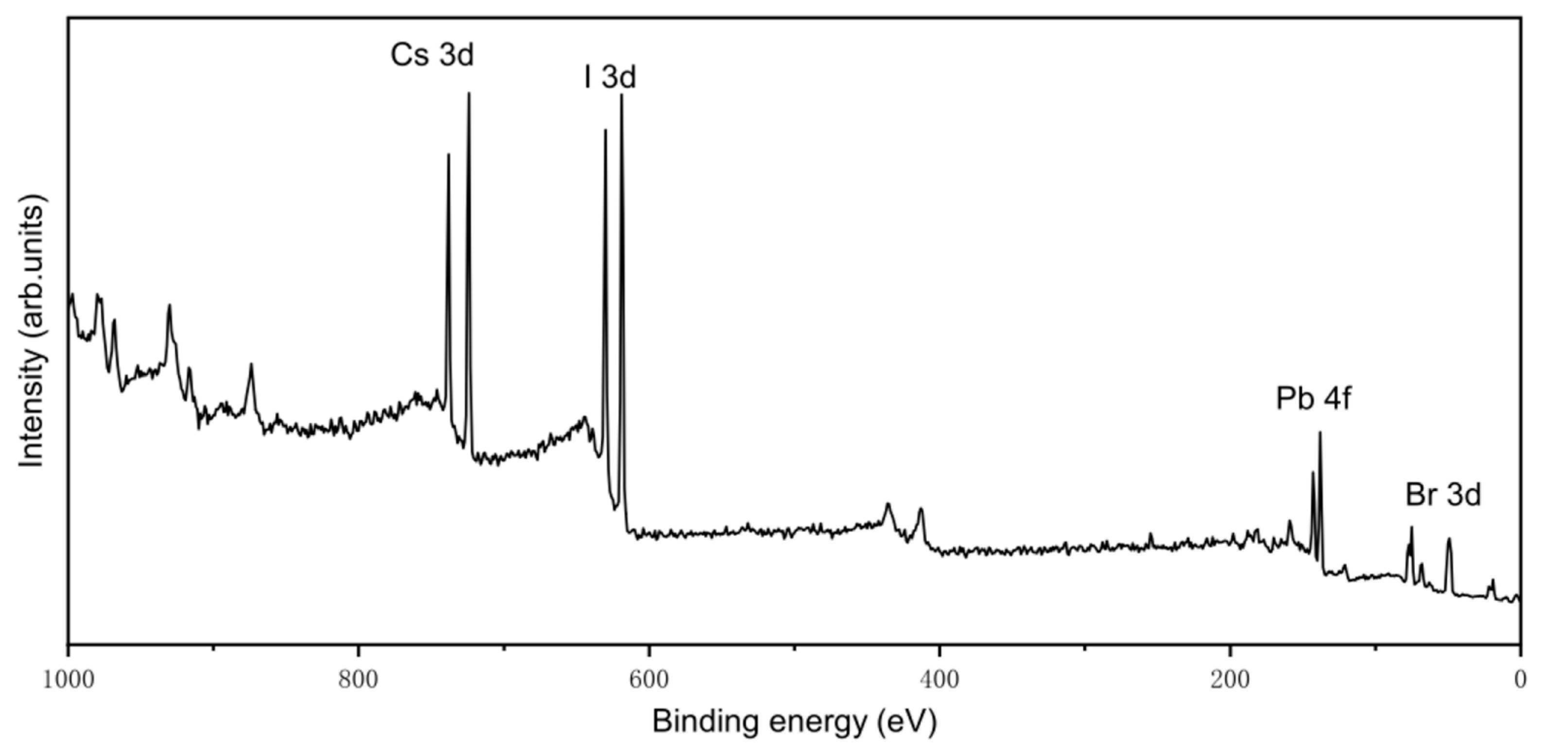
Figure A1.
The XPS survey spectrum of an as-prepared CsPbI2Br film.

References
- Kojima, A.; Teshima, K.; Shirai, Y.; Miyasaka, T. Organometal Halide Perovskites as Visible-Light Sensitizers for Photovoltaic Cells. J. Am. Chem Soc. 2009, 131, 6050–6051. [Google Scholar] [CrossRef] [PubMed]
- Green, M.A.; Dunlop, E.D.; Hohl-Ebinger, J.; Yoshita, M.; Kopidakis, N.; Hao, X. Solar cell efficiency tables (version 56). Prog. Photovolt. Res. Appl. 2020, 28, 629–638. [Google Scholar] [CrossRef]
- Snaith, H.J. Present status and future prospects of perovskite photovoltaics. Nat. Mater. 2018, 17, 372–376. [Google Scholar] [CrossRef]
- Chen, J.Z.; Choy, W.C.H. Efficient and Stable All-Inorganic Perovskite Solar Cells. Sol. RRL 2020, 4. [Google Scholar] [CrossRef]
- Eperon, G.E.; Stranks, S.D.; Menelaou, C.; Johnston, M.B.; Herz, L.M.; Snaith, H.J. Formamidinium lead trihalide: A broadly tunable perovskite for efficient planar heterojunction solar cells. Energy Environ. Sci. 2014, 7, 982–988. [Google Scholar] [CrossRef]
- Singh, A.; Lai, P.-T.; Mohapatra, A.; Chen, C.-Y.; Lin, H.-W.; Lu, Y.-J.; Chu, C.W. Panchromatic heterojunction solar cells for Pb-free all-inorganic antimony based perovskite. Chem. Eng. J. 2021, 419. [Google Scholar] [CrossRef]
- Usman, M.; Yan, Q. Recent Advancements in Crystalline Pb-Free Halide Double Perovskites. Crystals 2020, 10, 62. [Google Scholar] [CrossRef] [Green Version]
- Walkons, C.; Murshed, R.; Bansal, S. Numerical Analysis of Pb-Free Perovskite Absorber Materials: Prospects and Challenges. Sol. RRL 2020, 4. [Google Scholar] [CrossRef]
- Zhang, H.; Zhu, L.; Cheng, J.; Chen, L.; Liu, C.; Yuan, S. Morphologically Controlled Synthesis of Cs2SnCl6 Perovskite Crystals and Their Photoluminescence Activity. Crystals 2019, 9, 258. [Google Scholar] [CrossRef] [Green Version]
- Park, N.G.; Gratzel, M.; Miyasaka, T.; Zhu, K.; Emery, K. Towards stable and commercially available perovskite solar cells. Nat. Energy 2016, 1. [Google Scholar] [CrossRef]
- Boyd, C.C.; Cheacharoen, R.; Leijtens, T.; McGehee, M.D. Understanding Degradation Mechanisms and Improving Stability of Perovskite Photovoltaics. Chem. Rev. 2019, 119, 3418–3451. [Google Scholar] [CrossRef]
- Lee, J.W.; Kim, D.H.; Kim, H.S.; Seo, S.W.; Cho, S.M.; Park, N.G. Formamidinium and Cesium Hybridization for Photo- and Moisture-Stable Perovskite Solar Cell. Adv. Energy Mater. 2015, 5. [Google Scholar] [CrossRef]
- Wang, P.; Zhang, X.; Zhou, Y.; Jiang, Q.; Ye, Q.; Chu, Z.; Li, X.; Yang, X.; Yin, Z.; You, J. Solvent-controlled growth of inorganic perovskite films in dry environment for efficient and stable solar cells. Nat. Commun. 2018, 9, 2225. [Google Scholar] [CrossRef] [PubMed]
- Wang, Y.; Zhang, T.Y.; Kan, M.; Li, Y.; Wang, T.; Zhao, Y. Efficient α-CsPbI3 Photovoltaics with Surface Terminated Organic Cations. Joule 2018, 2, 2065–2075. [Google Scholar] [CrossRef] [Green Version]
- Beal, R.E.; Slotcavage, D.J.; Leijtens, T.; Bowring, A.R.; Belisle, R.A.; Nguyen, W.H.; Burkhard, G.; Hoke, E.T.; Mcgehee, M.D. Cesium Lead Halide Perovskites with Improved Stability for Tandem Solar Cells. J. Phys. Chem. Lett. 2016, 7, 746. [Google Scholar] [CrossRef] [PubMed]
- Goldschmidt, V.M. The laws of crystal chemistry. Naturwissenschaften 1926, 14, 477–485. [Google Scholar] [CrossRef]
- Shockley, W.; Queisser, H.J. Detailed Balance Limit of Efficiency of P-N Junction Solar Cells. J. Appl. Phys. 1961, 32, 510–519. [Google Scholar] [CrossRef]
- He, J.; Su, J.; Ning, Z.; Ma, J.; Zhou, L.; Lin, Z.; Zhang, J.; Liu, S.; Chang, J.; Hao, Y. Improved Interface Contact for Highly Stable All-Inorganic CsPbI2Br Planar Perovskite Solar Cells. ACS Appl. Energy Mater. 2020, 3, 5173–5181. [Google Scholar] [CrossRef]
- Chen, W.J.; Chen, H.Y.; Xu, G.Y.; Xue, R.M.; Wang, S.; Li, Y.; Li, Y. Precise Control of Crystal Growth for Highly Efficient CsPbI2Br Perovskite Solar Cells. Joule 2019, 3, 191–204. [Google Scholar] [CrossRef] [Green Version]
- Han, Y.; Zhao, H.; Duan, C.Y.; Yang, S.; Yang, Z.; Liu, Z.; Liu, S. Controlled n-Doping in Air-Stable CsPbI2Br Perovskite Solar Cells with a Record Efficiency of 16.79%. Adv. Funct. Mater. 2020, 30, 1909972. [Google Scholar] [CrossRef]
- Zhao, H.; Han, Y.; Xu, Z.; Duan, C.; Yang, S.; Yuan, S.; Yang, Z.; Liu, Z.; Liu, S. A Novel Anion Doping for Stable CsPbI2Br Perovskite Solar Cells with an Efficiency of 15.56% and an Open Circuit Voltage of 1.30 V. Adv. Energy Mater. 2019, 9, 1902279. [Google Scholar] [CrossRef]
- Zhao, H.; Yang, S.M.; Han, Y.; Yuan, S.H.; Jiang, H.; Duan, C.; Liu, Z.; Liu, S. A High Mobility Conjugated Polymer Enables Air and Thermally Stable CsPbI2Br Perovskite Solar Cells with an Efficiency Exceeding 15%. Adv. Mater. Technol. 2019, 4, 1900311. [Google Scholar] [CrossRef]
- Azmi, R.; Lee, C.L.; Jung, I.H.; Jang, S.Y. Simultaneous Improvement in Efficiency and Stability of Low-Temperature-Processed Perovskite Solar Cells by Interfacial Control. Adv. Energy Mater. 2018, 8. [Google Scholar] [CrossRef]
- Heo, J.H.; Lee, M.H.; Han, H.J.; Patil, B.R.; Yu, J.S.; Im, S.H. Highly efficient low temperature solution processable planar type CH3NH3PbI3 perovskite flexible solar cells. J. Mater. Chem. A 2016, 4, 1572–1578. [Google Scholar] [CrossRef]
- Liang, Z.Q.; Zhang, Q.F.; Wiranwetchayan, O.; Xi, J.; Yang, Z.; Park, K.; Li, C.; Cao, G. Effects of the Morphology of a ZnO Buffer Layer on the Photovoltaic Performance of Inverted Polymer Solar Cells. Adv. Funct. Mater. 2012, 22, 2194–2201. [Google Scholar] [CrossRef]
- Sun, Y.M.; Seo, J.H.; Takacs, C.J.; Seifter, J.; Heeger, A.J. Inverted Polymer Solar Cells Integrated with a Low-Temperature-Annealed Sol-Gel-Derived ZnO Film as an Electron Transport Layer. Adv. Mater. 2011, 23, 1679–1683. [Google Scholar] [CrossRef]
- Shen, E.C.; Chen, J.D.; Tian, Y.; Luo, Y.X.; Shen, Y.; Sun, Q.; Jin, T.Y.; Shi, G.Z.; Li, Y.Q.; Tang, J.X. Interfacial Energy Level Tuning for Efficient and Thermostable CsPbI2Br Perovskite Solar Cells. Adv. Sci. 2020, 7, 1901952. [Google Scholar] [CrossRef] [Green Version]
- Chen, S.; Goh, T.W.; Sabba, D.; Chua, J.; Mathews, N.; Huan, C.H.A.; Sum, T.C. Energy level alignment at the methylammonium lead iodide/copper phthalocyanine interface. APL Mater. 2014, 2. [Google Scholar] [CrossRef] [Green Version]
- Hanack, M.; Lang, M. Conducting Stacked Metallophthalocyanines and Related Compounds. Adv. Mater. 1994, 6, 819–833. [Google Scholar] [CrossRef]
- Uchida, S.; Xue, J.G.; Rand, B.P.; Forrest, S.R. Organic small molecule solar cells with a homogeneously mixed copper phthalocyanine: C60 active layer. Appl. Phys. Lett. 2004, 84, 4218–4220. [Google Scholar] [CrossRef]
- Van Slyke, S.A.; Chen, C.H.; Tang, C.W. Organic electroluminescent devices with improved stability. Appl. Phys. Lett. 1996, 69, 2160–2162. [Google Scholar] [CrossRef]
- Jun, W.; Haibo, W.; Jun, Y.X.; Huang, H.; Yan, D. Organic heterojunction and its application for double channel field-effect transistors. Appl. Phys. Lett. 2005, 87, 093507. [Google Scholar] [CrossRef]
- Zhang, S.S.; Wu, S.H.; Chen, W.T.; Zhu, H.M.; Xiong, Z.Z.; Yang, Z.C.; Chen, C.L.; Chen, R.; Han, L.Y.; Chen, W. Solvent engineering for efficient inverted perovskite solar cells based on inorganic CsPbI2Br light absorber. Mater. Today Energy 2018, 8, 125–133. [Google Scholar] [CrossRef]
- Chen, S.L.; Zhang, T.J.; Liu, X.L.; Qiao, J.L.; Peng, L.; Wang, J.; Liu, Y.S.; Yang, T.Y.; Lin, J. Lattice reconstruction of La-incorporated CsPbI2Br with suppressed phase transition for air-processed all-inorganic perovskite solar cells. J. Mater. Chem. C 2020, 8, 3351–3358. [Google Scholar] [CrossRef]
- Dong, C.; Han, X.X.; Zhao, Y.; Li, J.; Chang, L.; Zhao, W. A Green Anti-Solvent Process for High Performance Carbon-Based CsPbI2Br All-Inorganic Perovskite Solar Cell. Sol. RRL 2018, 2. [Google Scholar] [CrossRef]
- Wang, Q.-K.; Wang, R.-B.; Shen, P.-F.; Li, C.; Li, Y.-Q.; Liu, L.-J.; Duhm, S.; Tang, J.-X. Energy Level Offsets at Lead Halide Perovskite/Organic Hybrid Interfaces and Their Impacts on Charge Separation. Adv. Mater. Interfaces 2015, 2, 1400528. [Google Scholar] [CrossRef]
- Schwieger, T.; Peisert, H.; Golden, M.S.; Knupfer, M.; Fink, J. Electronic structure of the organic semiconductor copper phthalocyanine and K-CuPc studied using photoemission spectroscopy. Phys. Rev. B 2002, 66. [Google Scholar] [CrossRef]
- Dufour, G.; Poncey, C.; Rochet, F.; Roulet, H.; Sacchi, M.; De Santis, M.; De Crescenzi, M. Copper phthalocyanine on Si(111)-7 × 7 and Si(001)-2 × 1 surfaces: An X-ray photoemission spectroscopy and synchrotron X-ray absorption spectroscopy study. Surf. Sci. 1994, 319, 251–266. [Google Scholar] [CrossRef]
- Ottaviano, L.; DiNardo, S.; Lozzi, L.; Passacantando, M.; Picozzi, P.; Santucci, S. Thin and ultra-thin films of nickel phthalocyanine grown on highly oriented pyrolitic graphite: An XPS, UHV-AFM and air tapping-mode AFM study. Surf. Sci. 1997, 373, 318–332. [Google Scholar] [CrossRef]
- Oehzelt, M.; Koch, N.; Heimel, G. Organic semiconductor density of states controls the energy level alignment at electrode interfaces. Nat. Commun. 2014, 5, 4174. [Google Scholar] [CrossRef]
- Oehzelt, M.; Akaike, K.; Koch, N.; Heimel, G. Energy-level alignment at organic heterointerfaces. Sci. Adv. 2015, 1. [Google Scholar] [CrossRef] [Green Version]
- Mariotti, S.; Hutter, O.S.; Phillips, L.J.; Yates, P.J.; Kundu, B.; Durose, K. Stability and Performance of CsPbI2Br Thin Films and Solar Cell Devices. ACS Appl. Mater. Interfaces 2018, 10, 3750–3760. [Google Scholar] [CrossRef] [PubMed]
- Iwashita, M.; Yamanaka, S.; Tsuruta, R.; Tonami, K.; Yoshida, K.; Hayakawa, K.; Cojocaru, L.; Uchida, S.; Mase, K.; Nakayama, Y. Electronic structure of the clean interface between single crystal CH3NH3PbI3 and an organic hole transporting material spiro-OMeTAD. Appl. Phys. Lett. 2020, 116. [Google Scholar] [CrossRef]
- Liu, Z.; Sun, B.; Liu, X.; Han, J.; Ye, H.; Shi, T.; Tang, Z.; Liao, G. Efficient Carbon-Based CsPbBr3 Inorganic Perovskite Solar Cells by Using Cu-Phthalocyanine as Hole Transport Material. Nano-Micro Lett. 2018, 10, 34. [Google Scholar] [CrossRef] [PubMed] [Green Version]
- Zhang, X.; Yang, J.; Xie, L.; Lu, X.; Gao, X.; Gao, J.; Shui, L.; Wu, S.; Liu, J.-M. Boosting the performance of low-temperature processed CsPbI2Br planar perovskite solar cells by interface engineering. Dyes Pigment. 2021, 186. [Google Scholar] [CrossRef]
- Liu, Z.; Zhang, X.; Zhang, Y.; Jiang, J. Theoretical investigation of the molecular, electronic structures and vibrational spectra of a series of first transition metal phthalocyanines. Spectrochim. Acta Part A Mol. Biomol. Spectrosc. 2007, 67, 1232–1246. [Google Scholar] [CrossRef]
Figure 1.
(a) The SEM image; (b) 2D GIXRD pattern and (c) 1D GIXRD spectra derived from (b).

Figure 2.
(a) Cs 3d, (b) Pb 4f, (c) I 3d and (d) Br 3d core level spectra at the CuPc/CsPbI2Br interface. (e) The evolutions of core-levels as functions of CuPc thickness. The binding energies of the core-levels are referred to those of the pristine CsPbI2Br film.
Figure 2.
(a) Cs 3d, (b) Pb 4f, (c) I 3d and (d) Br 3d core level spectra at the CuPc/CsPbI2Br interface. (e) The evolutions of core-levels as functions of CuPc thickness. The binding energies of the core-levels are referred to those of the pristine CsPbI2Br film.

Figure 3.
Thickness-dependent (a) C 1s, (b) N 1s and (c) Cu 2p core-level spectra at CuPc/CsPbI2Br interface. The inset in panel a show the fitting curves for 117 Å CuPc film.
Figure 3.
Thickness-dependent (a) C 1s, (b) N 1s and (c) Cu 2p core-level spectra at CuPc/CsPbI2Br interface. The inset in panel a show the fitting curves for 117 Å CuPc film.

Figure 4.
(a) The VB and (b) SECO spectra at the CuPc/CsPbI2Br interface.

Figure 5.
(a) The relative energy level shifts of N 1s, Cu 2p, C 1s, CuPc HOMO and WF as functions of CuPc thickness. The energies refer to those of the 117 Å CuPc. (b) The energy level diagram at the CsPbI2Br/CuPc interface.
Figure 5.
(a) The relative energy level shifts of N 1s, Cu 2p, C 1s, CuPc HOMO and WF as functions of CuPc thickness. The energies refer to those of the 117 Å CuPc. (b) The energy level diagram at the CsPbI2Br/CuPc interface.

Publisher’s Note: MDPI stays neutral with regard to jurisdictional claims in published maps and institutional affiliations. |
© 2021 by the authors. Licensee MDPI, Basel, Switzerland. This article is an open access article distributed under the terms and conditions of the Creative Commons Attribution (CC BY) license (https://creativecommons.org/licenses/by/4.0/).
Share and Cite
MDPI and ACS Style
Tang, Z.; Zhang, L.; Su, Z.; Wang, Z.; Chen, L.; Wang, C.; Xiao, G.; Gao, X. A Study of Interfacial Electronic Structure at the CuPc/CsPbI2Br Interface. Crystals 2021, 11, 547. https://0-doi-org.brum.beds.ac.uk/10.3390/cryst11050547
AMA Style
Tang Z, Zhang L, Su Z, Wang Z, Chen L, Wang C, Xiao G, Gao X. A Study of Interfacial Electronic Structure at the CuPc/CsPbI2Br Interface. Crystals. 2021; 11(5):547. https://0-doi-org.brum.beds.ac.uk/10.3390/cryst11050547
Chicago/Turabian StyleTang, Zengguang, Liujiang Zhang, Zhenhuang Su, Zhen Wang, Li Chen, Chenyue Wang, Guoping Xiao, and Xingyu Gao. 2021. "A Study of Interfacial Electronic Structure at the CuPc/CsPbI2Br Interface" Crystals 11, no. 5: 547. https://0-doi-org.brum.beds.ac.uk/10.3390/cryst11050547
Note that from the first issue of 2016, this journal uses article numbers instead of page numbers. See further details here.