Article

Black Phosphorus-Molybdenum Disulfide Hetero-Junctions Formed with Ink-Jet Printing for Potential Solar Cell Applications with Indium-Tin-Oxide

by
Ravindra Ketan Mehta
1 and
Anupama Bhat Kaul
1,2,*
1
Department of Materials Science and Engineering, PACCAR Technology Institute, University of North Texas, Denton, TX 76203, USA
2
Department of Electrical Engineering, University of North Texas, Denton, TX 76203, USA
*
Author to whom correspondence should be addressed.
Submission received: 31 March 2021 / Revised: 7 May 2021 / Accepted: 12 May 2021 / Published: 18 May 2021
(This article belongs to the Special Issue Design, Characterization, and Application of 2D Materials)

Abstract

:
In this work, we implemented liquid exfoliation to inkjet-print two-dimensional (2D) black phosphorous (BP) and molybdenum disulfide (MoS2) p–n heterojunctions on a standard indium tin oxide (ITO) glass substrate in a vertical architecture. We also compared the optical and electrical properties of the inkjet-printed BP layer with that of the MoS2 and the electrical properties of the mechanically exfoliated MoS2 with that of the inkjet-printed MoS2. We found significant differences in the optical characteristics of the inkjet-printed BP and MoS2 layers attributed to the differences in their underlying crystal structure. The newly demonstrated liquid exfoliated and inkjet-printed BP–MoS2 2D p–n junction was also compared with previous reports where mechanically exfoliated BP–MoS2 2D p–n junction were used. The electronic transport properties of mechanically exfoliated MoS2 membranes are typically better compared to inkjet-printed structures but inkjet printing offers a cost-effective and quicker way to fabricate heterostructures easily. In the future, the performance of inkjet-printed structures can be further improved by employing suitable contact materials, amongst other factors such as modifying the solvent chemistries. The architecture reported in this work has potential applications towards building solar cells with solution processed 2D materials in the future.

1. Introduction

The family of two-dimensional (2D) materials comprising graphene [1], MoS2 [2,3], WSe2 [4], and black phosphorus (BP) [5,6] have gained phenomenal interest in electronics, optoelectronic devices, sensors, and solar cells [7,8,9,10,11]. Among the various 2D materials, BP is a monoelemental van der Waals solid with a thickness-dependent direct bandgap which ranges from 0.3 eV in the bulk to about 2.0 eV for the single-layer BP flake [6,12]. The transistors fabricated from mechanically exfoliated BP are found to possesses high ON/OFF ratios [13,14], and high mobilities (200–1000 cm2 V−1 s−1) at room temperature, compared to transition metal dichalcogenides (TMDs) [7,15]. Therefore, BP has attracted a great deal of attention for the research community and the electronics industry, to potentially use its exceptional properties in areas such as field-effect transistors (FETs) [16], photodetectors [17,18], and flexible optoelectronics [19,20,21]. Bulk BP, similar to other TMDCs, can be cleaved into its constituent layers through mechanical [22,23,24] or liquid-phase exfoliation [25,26]. Apart from the ability of liquid exfoliation to yield large quantities of nanosheets, it also has added advantages such as solution processability with the manufacture of devices on a wide variety of substrates, including in composite formats. In prior work [25], it was demonstrated that liquid exfoliation of BP by sonication in organic solvents, such as N-cyclohexyl-2-pyrrolidone (CHP), can stabilize the BP layer and provide a high yield of flakes. Compared with mechanically exfoliated BP sheets, liquid-phase exfoliated BP is remarkably stable in CHP. It is anticipated that the tightly packed solvation shells in close proximity to the BP surface act as a protective barrier against moisture and oxygen that are known to deter the remarkable properties of BP [25]. With MoS2, one of the most well-studied 2D TMDs, a thickness-dependent bandgap results that transitions from direct to indirect bandgap from 1.9 (monolayer) to 1.23 eV (bulk) [26].
Two-dimensional crystalline heterostructures created by stacking atomic layers of different materials on top of each other can push scaling limits of these materials by allowing the ability to form monolayer thick tunneling barriers and quantum wells [27]. Two-dimensional mechanically exfoliated vertical p–n junctions of BP–MoS2 on oxidized Si wafers have already been studied, but there are no prior reports on liquid exfoliated and inkjet-printed BP–MoS2 2D p–n junctions on indium tin oxide (ITO) coated glass substrates, which would form a first step toward their integration into electronics and photovoltaics platforms. Recently, transistors made from the combination of inkjet-printed graphene and MoS2 channel have shown good Ion/Ioff ratios of 336 [28].Materials such as ITO serve as a good bottom contact for the device since it provides better adhesion, conductivity, and transmittance compared to other transparent conductive oxides with notable examples being zinc oxide (ZnO) and aluminum-doped zinc oxide (AZO) [29]. In solar cells, fore contacts must have n-type conductivity and thus ITO is used as a bottom contact to allow transmission of light into the solar cells while enabling electrical conductivity at the same time. The enhanced optical properties of ITO allow enhanced photocarrier generation since a large fraction of the incoming light can be transmitted through it [29].
The 2D p–n junction heterostructure can be stacked either vertically or laterally. The vertical architecture attracts the most attention because 2D materials can be easily stacked vertically due to minimal dangling bonds through the weak van der walls interaction [30]. The band offset is also one of the critical parameters to be considered for designing 2D heterostructures. In a mono-epitaxial layer of graphene, Pierucci et al. [31] noticed the formation of miniband gaps. The miniband gaps are formed due to the periodic moire pattern between the MoS2 and graphene layers and band anticrossing occurring at the edge of the Brillouin zone [31]. The electrical transport characteristic at the interface of 2D/3D materials is governed by the thickness of the 2D material. Due to the formation of the metal-MoS2 Schottky barrier, rectifying behavior is observed for few-layer MoS2 on n-GaN substrates [32]. The van der Waals heterostructure alters the band alignment of graphene and other 2D materials [33], and in some cases the band edges shift up by 0.5 eV [34]. Inkjet printing is a versatile technique for the cost-effective and large-scale fabrication of heterostructures on a wide variety of substrates, unlike the mechanical exfoliation technique [35]. The flakes obtained by mechanical exfoliation are typically of better crystalline quality, but this technique is not scalable, but serves as a good reference for comparative analysis. On the other hand, inkjet-printing is scalable and well-tuned to large-scale manufacturability. It also allows tremendous flexibility to design structures such as sensor arrays and heterostructures of any geometry in both planar and vertical directions [36]. Inkjet-printing remains at the forefront amongst non-contact-digital fabrication technologies, offering the flexibility to print arbitrary design patterns at will, where the research has been translated to large-scale industrial applications [37]. Moreover, inkjet-printing has the capability to form individual pixels and is a material effective technique [38]. It has also been used to form arrays of molecular tunnel junction [39].
In this work, BP–MoS2 2D p–n junctions were formed and vertically stacked on top of each other using solution-processed inkjet-printing on a standard ITO glass substrate. The electrical behavior of the inkjet-printed BP–MoS2 2D p–n junction was evaluated and the electrical and optical behavior of individual layers was also examined. Moreover, we also compared the electrical behavior of mechanically exfoliated MoS2 with that of the inkjet-printed MoS2. This work should provide a good framework for using solution processed heterojunctions of MoS2 and BP on ITO substrates for future solar cell platforms.

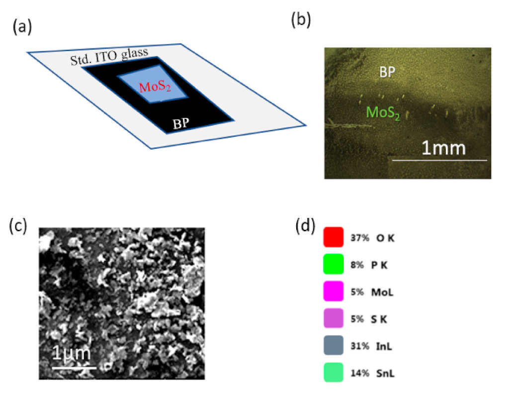
2. Materials and Methods

2.1. Liquid Exfoliation and Inkjet-Printing of Black Phosphorus Layer

The BP crystals were purchased from a commercial supplier (Smart-Elements) and stored in an Argon (Ar)-purged glovebox system where the oxygen and moisture levels were carefully controlled to be less than 0.1 ppm. The solvent used for the exfoliation was N-cyclohexyl-2-pyrrolidone (CHP), which was purchased from Sigma-Aldrich. The CHP solvent increases the oxidation resistance of BP by forming a solvation shell around it [25]. For liquid-phase exfoliation, BP crystal was finely ground into a powder form inside the glove box. The 60 mg of finely grounded powder was then mixed with 12 mL of CHP inside a conical tube filled with nitrogen (N2) gas. The interface between the cap and the conical tube was sealed several times with Teflon tape and parafilm was found to be instrumental in preventing O2 and H2O to seep into the conical tube. The dispersion was sonicated for 24 hours under cooling in a Branson CPX 2800 bath sonicator (Fisher Scientific USA, Waltham, MA, USA) at ambient conditions. As-prepared BP dispersions were centrifuged at five different centrifugation rates ranging from 1000 up to 10,000 rpm for 10 min, using an Eppendorf Centrifuge 5804 (Hamburg, Germany) to remove bulk and unexfoliated BP layers. The 5 mL supernatant solution was taken out from the conical tube centrifuged at 1000 rpm for 10 min and transferred to the cartridge used for inkjet-printing. The viscosity of BP ink measured using the AMETEK DV3T Brookfield viscosity meter (Berwyn, IL, USA) was 10.82 cP, which is ideally tailored for inkjet printing with the Dimatix Fujifilm 2850 material printer (Santa Clara, CA, USA). The standard ITO glass substrates obtained from Sigma-Aldrich had a 120 nm thick ITO thin film and a surface resistivity of 8 ohms/sq. The substrate was cleaned by sonication in acetone, isopropyl alcohol (IPA), and deionized (DI) water for 5 min, followed by 15 min of UV ozone cleaning. The BP in CHP dispersion was inkjet-printed on the standard ITO glass substrate with a drop spacing of 20 µm and 40 passes were used to print the structures on top of each other. The BP layer was printed over a 5 mm by 3 mm rectangular area, and due to fluidic surface tension effects of the CHP ink with the ITO, the printed BP film took an elliptical shape with a smaller area. The printed BP film on the standard ITO glass substrate was then vacuum annealed at 70 °C for 30 min hold time, 250 °C for 90 min hold time, and 300 °C for 60 min hold time at a pressure of 5 m·Torr with a thermal ramp rate of 5 °C/min to evaporate the solvent and enhance the electrical conductivity.

2.2. Liquid Exfoliation and Inkjet-Printing of MoS2 on Top of the BP Layer

The MoS2 powder was purchased from Sigma-Aldrich. A mixture of cyclohexanone/terpineol (C/T) was used as an exfoliation solvent. Cyclohexanone was purchased from Acros organics and the terpineol was from Sigma-Aldrich. A mixture of 7 mL cyclohexanone and 3 mL terpineol was prepared by withdrawing the solvents using a micropipette and then 0.2 g of ethyl cellulose (EC) purchased from Sigma-Aldrich was mixed with the C/T mixture. The resultant mixture was sonicated for about 45 min until the EC completely dissolved in the C/T mixture. Ethyl cellulose is used as a surfactant that facilitates the exfoliation of MoS2 into nanosheets by preventing the reagglomeration of the nanosheets and controlling the viscosity of the dispersion. The MoS2 powder was then finely ground using a mortar and pestle and 300 mg of the finely grounded powder was mixed with the EC dissolved in the C/T solvent. The resultant dispersion was sonicated for 48 hours under cooling in a Branson bath sonicator at ambient conditions. The as-prepared dispersion was centrifuged in a conical tube at 1000 rpm for 10 min to remove bulk and unexfoliated MoS2 layers. The 5 mL supernatant solution was then taken out from the conical tube and transferred to the cartridge used for inkjet-printing. The viscosity of the MoS2 ink measured after centrifugation was 9.55 cP. The MoS2 in the C/T dispersion was inkjet-printed on top of the BP layer with a drop spacing of 40 µm and again, 40 passes were used. The MoS2 was printed over a square of 2 mm in length, but again due to fluidic surface tension effects with the C/T MoS2 ink over the underlying BP layer, the printed MoS2 layer was geometrically distorted from the designed parameters. The printed MoS2 film on the BP layer was then vacuum annealed using the following thermal profile: ramp up to 120 °C for 40 min hold time, 220 °C for 20 min hold time, and finally 350 °C for 120 min hold time at 5 m·Torr of pressure at a ramp rate of ~5 °C/min in order to evaporate the solvent to form a densified film.

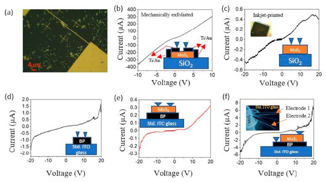
2.3. Mechanical Exfoliation of MoS2 and Electron Beam Lithography to Form the Contacts

The 75 mm oxidized Si wafer was cleaved into a smaller 2 cm × 2 cm samples and then cleaned in acetone, IPA, and DI water for 5 min each, followed by surface treatment with UV ozone for 15 min. The MoS2 bulk crystal was first exfoliated multiples times using blue-tac tape into thinner flakes until it was eventually transferred onto the oxidized Si wafer. The PMMA used for e-beam lithography was spin-coated on the exfoliated sample using a two-step process, where the first step is to uniformly coat the sample at 500 rpm initially, followed by a 1000 rpm/s for a duration of 10 s. In the second step, the solvent was evaporated at 1500 rpm, followed by a further increment to 2000 rpm/s for 60 s. Soft baking was conducted at 180 °C for 90 s to drive off the trapped solvents. The e-beam pattern was written using the JEOL JSM-7001F Scanning electron microscope (Peabody, MA, USA) and XENOS pattern generator (Waalwijk, The Netherlands) at a dose of 180 µC/cm2 and 15 keV electron energy in a class 100 cleanroom. The pattern development was done by immersing the sample in a mixture of IPA and DI water at a ratio of 20:1 for 30 s. Metal electrodes comprising of 100 nm of Au were deposited over a 10 nm thick Ti adhesion layer using electron beam evaporation, using a metal lift-off process, where the underlying PMMA was dissolved with acetone in a squirt bottle.

3. Results and Discussion

To build the heterostructures, we first prepared the BP ink and inkjet-printed BP on the standard (std.). ITO glass substrate, so that the MoS2 layer above printed thereafter protects the BP layer against oxidation. We sonicated the BP dispersion for 24 h with a nitrogen filled balloon surrounding the dispersion as shown in Figure 1a. Figure 1b depicts the color of the dispersion after sonication at various centrifugation speeds ranging from 2000 rpm, 5000 rpm, 8000 rpm, and 10,000 rpm was conducted for 10 min. The resulting stable BP dispersions possess a dark brown to yellow color, as seen in Figure 1c. The BP dispersion obtained after 24 h of sonication and centrifugation at 1000 rpm for 10 min. is seen in Figure 1d, which reveals a stable dark dispersion suitable for inkjet-printing.
The scanning electron microscope (SEM) images and energy dispersive spectroscopy (EDS) elemental mapping of the layers were obtained using an FEI Quanta 200 Environmental (e-) SEM (Hillsboro, OR, USA). The Raman and photoluminescence (PL) data were obtained using a Horiba LabRAM HR Evolution (Kyoto, Japan), where the excitation laser wavelength used was 532 nm. Ultraviolet (UV)–visible (VIS) optical absorption spectroscopy was conducted using the CARY 5000 spectrophotometer (Oldsmar, FL, USA) in quartz cuvettes with 0.3 mL volumetric capacity. The electrical characteristics of the devices were measured with a micromanipulator 450PM-B probe stage equipped with an Agilent/Keysight precision semiconductor parameter analyzer 4156A (Santa Rosa, CA, USA). A Lakeshore CRX-4K probe station (Westerville, OH, USA) was used to obtain the IV data for mechanically exfoliated flakes with a Keysight B1500-A semiconductor device analyzer.
The absorption spectrum of the BP flakes exfoliated in CHP followed by centrifugation at 1000 rpm is shown in Figure 2a in arbitrary units (a.u.), where the enhanced absorption at lower wavelengths corroborates the quantum confinement effects arising in the thinner BP platelets. The position of the absorption peak is dependent on the thickness of the BP layer. The absorption spectrum of the BP dispersion observed in this study is blue-shifted by 40 nm, i.e., the peak shifts from 260 nm as obtained in this study, compared to the absorption spectra of the bulk BP shown by Xu, et al. [40], where the peak was obtained at 300 nm, indicating the presence of few-layer black phosphorus. Raman and PL spectroscopy are powerful techniques to characterize various 2D materials. The optoelectronic properties of the black phosphorous and MoS2 depend on their thicknesses [26]. In Figure 2b, the inkjet-printed BP shows the Raman peaks occurring at 361.0 cm−1, 436.9 cm−1, and 464.3 cm−1 wavenumbers, which correspond to the locations of the A1g, B2g, and A2g phonon modes, respectively, for a few layers of BP. The B2g and A2g phonon modes vibrate in-plane, whereas the A1g phonon modes vibrate out-of-plane for BP. The bottom-left inset in Figure 2b shows the optical microscope image of the BP flakes where the Raman and PL spectra were obtained, and the representation of the atomic arrangement of the three vibrational modes depicting the characteristic puckered structure of BP is illustrated in the top-left inset of Figure 2b.
The number of atomic layers in the black phosphorus can also be characterized by the difference in frequency between the two out-of-plane vibrational modes, i.e., B2g and Ag2 modes. The frequency difference between the two out-of-plane vibrational modes Δk of the inkjet-printed black phosphorus, as shown in Figure 2a, is 30 cm−1, which lies within that of bulk (27.7 cm−1) and monolayer black phosphorus (31 cm−1), and thus, we surmise that the inkjet-printed BP is at least a few layers thick [41]. Figure 2c shows the Raman spectra of inkjet-printed MoS2 on top of the BP layer with the E12g and A1g phonon vibrational modes with a wavenumber difference of 24.8 cm−1. The right inset in Figure 2c shows the optical microscope image of the MoS2 flake where the Raman and PL spectra were obtained, along with the MoS2 structure in the left inset, where the Mo atom is sandwiched between the two S atoms. The E12g mode refers to the in-plane vibrations while the A1g represents the out-of-plane phonon vibrations of the atoms in the MoS2 crystal structure. Figure 2d depicts the PL spectra of inkjet-printed BP on the standard ITO glass substrate and inkjet-printed MoS2 on BP. The bandgap of BP is 1.93 eV and that of MoS2 is 1.68 eV indicating few-layers present for both materials. The full-width half maxima (FWHM) of BP were measured to be 93 meV and that of MoS2 is 252 meV, which is about 2.7 times higher than that of the BP layer. The lower FWHM of BP compared to that of the MoS2 is likely to arise from the more tightly bound atoms in BP’s puckered structure compared to MoS2 and the presence of a higher defect density in the latter, compared to BP [42].
The BP has an intrinsically p-type conduction whereas MoS2 has an intrinsically n-type conduction as corroborated by prior studies [2,26]. Figure 3a shows the schematic cross-section of the inkjet-printed vertical 2D p–n junction heterostructure device where the layers are printed to form a stack. Figure 3b shows the optical micrograph of the inkjet-printed structure from the top. The irregularity in the printed structure is due to surface tension effects of the C/T MoS2 ink with that of the CHP ink with BP. The darker region represents the MoS2 whereas the brighter one represents BP. Figure 3c shows a top-view high magnification SEM image of the inkjet-printed overlying MoS2 layer, where cluster like platelets uniformly appear to cover the BP layer underneath it. The EDS elemental distribution in Figure 3d taken over a 60 µm × 60 µm area further confirms the presence of BP and MoS2 layers along with the presence of indium, tin, and oxygen from the underlying ITO substrate.
Figure 4a shows the optical micrograph of mechanically exfoliated MoS2 on the oxidized silicon substrate with Au/Ti contact electrodes on either end. Figure 4b shows the current–voltage characteristic of the mechanically exfoliated MoS2 membrane probed on the oxidized Si wafer with the electron beam lithography (EBL) patterned electrodes as from Figure 4a. The interconnect spacing on the membrane was 5 µm. The electrical behavior is mostly linear with some non-linearity at near-zero voltages. Figure 4c shows the electrical behavior of the inkjet-printed MoS2 printed over 2 mm square on the oxidized silicon wafer, where the inset shows the optical image of the inkjet-printed MoS2 on the oxidized Si wafer. The printed structure of the MoS2 was almost the same geometry and dimensions as specified as opposed to the distorted geometry and dimensions of inkjet-printed MoS2 on the underlying BP layer where the surface tension and viscosity of the CHP and C/T inks is in the printable range. As seen the MoS2 printed on the BP layer has distorted geometry than the specified whereas the MoS2 printed on the oxidized silicon substrate in printed with the same geometry as specified. The MoS2 layer printed on the oxidized silicon substrate was printed with the exact dimensions as specified, this further reinforces our claim that the surface tension mismatch was the reason behind the distorted geometry of MoS2 printed on BP layers since the surface tension of MoS2 with C/T ink more closely matches with the oxidized silicon substrate as opposed to the BP with CHP ink.
The electrical behavior of the inkjet-printed MoS2 on the oxidized Si wafer in Figure 4c was obtained by direct probing the layer where the probe spacing was 200 µm. Reducing the spacing of the probes did not increase the magnitude of the current, on the contrary, the current magnitude further decreased, which could be due to the non-uniform topography of the printed structure. Compared to the inkjet-printed MoS2 on the oxidized Si wafer, the magnitude of the current was about 1000 times higher for the mechanically exfoliated MoS2 flake at the same voltage. The electrical behavior of the mechanically exfoliated and contacted flake shows nearly ohmic characteristics due to the ohmic contacts formed by the 100 nm Au over the 10 nm Ti (adhesion layer) with MoS2. Moreover, the inkjet-printed structure has some noise in the current–voltage characteristic whereas the mechanically exfoliated flake shows a smooth curve. The superior electrical characteristic of the mechanically exfoliated flake is due to the higher crystalline quality of the mechanically exfoliated flake and the excellent interface quality of the metal contact and the flake. On the contrary, the relatively poor electrical characteristic of the inkjet-printed MoS2 layer is due to the defects induced during the exfoliation process and trapped residual solvent and surfactant.
The quasisymmetric non-linear behavior observed in the inkjet-printed BP and MoS2 layers in Figure 4d,e is due to the Schottky barrier formed at the interface of the tungsten electrode probes and BP and MoS2 layers. Due to the relatively higher trap states and defect densities in the inkjet-printed MoS2 compared to inkjet-printed BP and a higher Schottky barrier height at the interface of MoS2 and the tungsten probes compared to BP and tungsten probes, the current almost remains constant until moderate voltages have been built up in the MoS2; however, at high voltages there is sufficient energy for the electrons to be able to tunnel through the barrier and conduct, and so, the current increases steeply after that.
Figure 4f shows the electrical behavior across the BP–MoS2 p–n junction interface. The device shows a non-ideal diode-like character. The rectification ratio was obtained by taking the modulus of the ratio of forward current and reverse current at ±20 V. The rectification ratio is given as Ifwd/IRev [32]. The rectification ratio obtained was 1.137. The ideality factor of this p–n junction was calculated using the equation: η = q KT × dV dlnI [43], where q is the charge of electron, i.e., 1.6 × 10⁻¹⁹ C, T is 300 K, assumed to be room temperature, and dV dlnI is the slope of the voltage versus natural log of current. The ideality factor obtained after the calculation was 8.88, which indicates the inkjet-printed p–n junction considerably deviates from the ideal diode equation. The rectification ratio obtained in this study is about three orders of magnitude less than the one reported by Deng, Y. et al. [44], where devices were made using mechanically exfoliated BP–MoS2 2D p–n junction as opposed to the liquid exfoliated and inkjet-printed BP–MoS2 heterojunctions in this study. The lower rectification ratio observed in this study is likely due to the ultra-thin size of the flakes in the liquid exfoliated and inkjet-printed structure compared to the mechanically exfoliated flakes resulting in increased dominance of electrons tunneling across the barrier at the interface of BP and MoS2 [45]. A slightly high value of ideality factor indicates the possibility of the charge traps and defect densities across the BP–MoS2 interface, which may have occurred due to the interdiffusion of the layers across the interface during the vacuum annealing step. The ideality factor can be further reduced by improvising on the contact materials for the BP and MoS2 layers, which can minimize the detrimental effects due to interfacial trap states.

4. Conclusions

We demonstrated the inkjet-printed BP-MoS2 vertical 2D p–n junction on std. ITO glass substrates, where a comparison of the electrical behavior of the inkjet-printed MoS2 with that of the mechanically exfoliated MoS2 flake was made. The superior electrical behavior of the mechanically exfoliated MoS2 is due to the superior crystalline quality of the flake compared to the liquid exfoliated and inkjet-printed MoS2 layer and high-quality contacts resulting in reduced interfacial defects. The lower rectification ratio observed in the BP–MoS2 2D p–n junction is due to the ultra-thin flakes. The ideality factor of the junction can be further reduced through contact engineering to minimize the effect of interfacial trap states. The inkjet-printed vertical architecture demonstrated has potential applications in the future towards solar cell platforms.

Author Contributions

Conceptualization, A.B.K.; Experimental Methodology; R.K.M.; Results Analysis and Discussion, R.K.M. and A.B.K. Both authors have read and agreed to the published version of the manuscript.

Funding

This research was funded by the Office of Naval Research (ONR) (Grant No. ONR N00014-19-1-2142) and the PACCAR Technology Institute at the University of North Texas.

Data Availability Statement

The data presented in this study are available on request from the corresponding author.

Acknowledgments

We thank the Office of Naval Research (ONR) (Grant No. ONR N00014-19-1-2142) that enabled us to pursue this work. R.K.M. also acknowledges the assistance provided by Misook Min in acquiring some of the images in Figure 1. A.B.K. is grateful to the support received from the University of North Texas (UNT) PACCAR Technology Institute and Endowed Professorship support.

Conflicts of Interest

The authors declare no conflict of interest.

References

  1. Novoselov, K.S.; Fal’ko, V.I.; Colombo, L.; Gellert, P.R.; Schwab, M.G.; Kim, K. A roadmap for graphene. Nature 2012, 490, 192–200. [Google Scholar] [CrossRef] [PubMed]
  2. Kaul, A.B. Two-dimensional layered materials: Structure, properties, and prospects for device applications. J. Mater. Res. 2014, 29, 348–361. [Google Scholar] [CrossRef] [Green Version]
  3. Michel, M.; Biswas, C.; Kaul, A.B. High-performance ink-jet printed graphene resistors formed with environmentally-friendly surfactant-free inks for extreme thermal environments. Appl. Mater. Today 2017, 6, 16–21. [Google Scholar] [CrossRef]
  4. Desai, J.A.; Adhikari, N.; Kaul, A.B. Chemical exfoliation efficacy of semiconducting WS2 and its use in an additively manufactured heterostructure graphene–WS2–graphene photodiode. RSC Adv. 2019, 9, 25805–25816. [Google Scholar] [CrossRef] [Green Version]
  5. Min, M.; Hossain, R.F.; Adhikari, N.; Kaul, A.B. Inkjet-Printed Organohalide 2D Layered Perovskites for High-Speed Photodetectors on Flexible Polyimide Substrates. ACS Appl. Mater. Interfaces 2020, 12, 10809–10819. [Google Scholar] [CrossRef] [PubMed]
  6. Min, M.; Sakri, S.; Saenz, G.A.; Kaul, A.B. Photophysical Dynamics in Semiconducting Graphene Quantum Dots Integrated with 2D MoS2 for Optical Enhancement in the Near UV. ACS Appl. Mater. Interfaces 2021, 13, 5379–5389. [Google Scholar] [CrossRef]
  7. Qiao, J.; Kong, X.; Hu, Z.-X.; Yang, F.; Ji, W. High-mobility transport anisotropy and linear dichroism in few-layer black phosphorus. Nat. Commun. 2014, 5, 4475–4481. [Google Scholar] [CrossRef] [PubMed] [Green Version]
  8. Liu, H.; Du, Y.; Deng, Y.; Ye, P.D. Semiconducting black phosphorus: Synthesis, transport properties and electronic applications. Chem. Soc. Rev. 2015, 44, 2732–2743. [Google Scholar] [CrossRef] [Green Version]
  9. Mas-Ballesté, R.; Gómez-Navarro, C.; Gómez-Herrero, J.; Zamora, F. 2D materials: To graphene and beyond. Nanoscale 2011, 3, 20–30. [Google Scholar] [CrossRef]
  10. Xia, F.; Wang, H.; Jia, Y. Rediscovering black phosphorus as an anisotropic layered material for optoelectronics and electronics. Nat. Commun. 2014, 5, 4458–4463. [Google Scholar] [CrossRef] [Green Version]
  11. Abbas, A.N.; Liu, B.; Chen, L.; Ma, Y.; Cong, S.; Aroonyadet, N.; Köpf, M.; Nilges, T.; Zhou, C. Black Phosphorus Gas Sensors. ACS Nano 2015, 9, 5618–5624. [Google Scholar] [CrossRef] [PubMed]
  12. Tran, V.; Soklaski, R.; Liang, Y.; Yang, L. Layer-controlled band gap and anisotropic excitons in few-layer black phosphorus. Phys. Rev. B 2014, 89, 235319–235324. [Google Scholar] [CrossRef] [Green Version]
  13. Youngblood, N.; Chen, C.; Koester, S.J.; Li, M. Waveguide-integrated black phosphorus photodetector with high responsivity and low dark current. Nat. Photon. 2015, 9, 247–252. [Google Scholar] [CrossRef]
  14. Andres, C.-G.; Leonardo, V.; Elsa, P.; Joshua, O.I.; Narasimha-Acharya, K.L.; Sofya, I.B.; Dirk, J.G.; Michele, B.; Gary, A.S.; Alvarez, J.V.; et al. Isolation and characterization of few-layer black phosphorus. 2D Mater. 2014, 1, 025001–025019. [Google Scholar]
  15. Fei, R.; Yang, L. Strain-Engineering the Anisotropic Electrical Conductance of Few-Layer Black Phosphorus. Nano Lett. 2014, 14, 2884–2889. [Google Scholar] [CrossRef] [PubMed] [Green Version]
  16. Du, Y.; Liu, H.; Deng, Y.; Ye, P.D. Device Perspective for Black Phosphorus Field-Effect Transistors: Contact Resistance, Ambipolar Behavior, and Scaling. ACS Nano 2014, 8, 10035–10042. [Google Scholar] [CrossRef] [Green Version]
  17. Yuan, H.; Liu, X.; Afshinmanesh, F.; Li, W.; Xu, G.; Sun, J.; Lian, B.; Curto, A.G.; Ye, G.; Hikita, Y.; et al. Polarization-sensitive broadband photodetector using a black phosphorus vertical p–n junction. Nat. Nanotechnol. 2015, 10, 707–713. [Google Scholar] [CrossRef] [Green Version]
  18. Huang, M.; Wang, M.; Chen, C.; Ma, Z.; Li, X.; Han, J.; Wu, Y. Broadband Black-Phosphorus Photodetectors with High Responsivity. Adv. Mater. 2016, 28, 3481–3485. [Google Scholar] [CrossRef]
  19. Zhu, W.; Yogeesh, M.N.; Yang, S.; Aldave, S.H.; Kim, J.-S.; Sonde, S.; Tao, L.; Lu, N.; Akinwande, D. Flexible Black Phosphorus Ambipolar Transistors, Circuits and AM Demodulator. Nano Lett. 2015, 15, 1883–1890. [Google Scholar] [CrossRef]
  20. Hao, C.; Yang, B.; Wen, F.; Xiang, J.; Li, L.; Wang, W.; Zeng, Z.; Xu, B.; Zhao, Z.; Liu, Z.; et al. Flexible All-Solid-State Supercapacitors based on Liquid-Exfoliated Black-Phosphorus Nanoflakes. Adv. Mater. 2016, 28, 3194–3201. [Google Scholar] [CrossRef]
  21. Zhu, W.; Park, S.; Yogeesh, M.N.; McNicholas, K.M.; Bank, S.R.; Akinwande, D. Black Phosphorus Flexible Thin Film Transistors at Gighertz Frequencies. Nano Lett. 2016, 16, 2301–2306. [Google Scholar] [CrossRef] [PubMed]
  22. Koenig, S.P.; Doganov, R.A.; Schmidt, H.; Neto, A.H.C.; Özyilmaz, B. Electric field effect in ultrathin black phosphorus. Appl. Phys. Lett. 2014, 104, 103106–103109. [Google Scholar] [CrossRef] [Green Version]
  23. Li, L.; Yu, Y.; Ye, G.J.; Ge, Q.; Ou, X.; Wu, H.; Feng, D.; Chen, X.H.; Zhang, Y. Black phosphorus field-effect transistors. Nat. Nanotechnol. 2014, 9, 372–377. [Google Scholar] [CrossRef] [PubMed] [Green Version]
  24. Li, L.; Kim, J.; Jin, C.; Ye, G.J.; Qiu, D.Y.; da Jornada, F.H.; Shi, Z.; Chen, L.; Zhang, Z.; Yang, F.; et al. Direct observation of the layer-dependent electronic structure in phosphorene. Nat. Nanotechnol. 2016, 12, 21–25. [Google Scholar] [CrossRef] [PubMed] [Green Version]
  25. Hanlon, D.; Backes, C.; Doherty, E.; Cucinotta, C.S.; Berner, N.C.; Boland, C.; Lee, K.; Harvey, A.; Lynch, P.; Gholamvand, Z.; et al. Liquid exfoliation of solvent-stabilized few-layer black phosphorus for applications beyond electronics. Nat. Commun. 2015, 6, 8563–8573. [Google Scholar] [CrossRef]
  26. Sahoo, D.; Kumar, B.; Sinha, J.; Ghosh, S.; Roy, S.S.; Kaviraj, B. Cost effective liquid phase exfoliation of MoS 2 nanosheets and photocatalytic activity for wastewater treatment enforced by visible light. Sci. Rep. 2020, 10, 1–12. [Google Scholar]
  27. Bonaccorso, F. Ink-jet printed 2D crystal heterostructures. In Proceedings of the 47th European Solid-State Device Research Conference (ESSDERC), Leuven, Belgium, 11–14 September 2017. [Google Scholar]
  28. Jewel, M.U.; Mokhtari-Koushyar, F.; Chen, R.T.; Chen, M.Y. All Inkjet-Printed High On/Off Ratio Two-Dimensional Materials Field Effect Transistor. In Proceedings of the IEEE 18th International Conference on Nanotechnology (IEEE-NANO), Cork, Ireland, 23–26 July 2018. [Google Scholar]
  29. Mehta, R.; Min, M.; Kaul, A.B. Sol-gel synthesized indium tin oxide as a transparent conductive oxide with solution-processed black phosphorus for its integration into solar cells. J. Vac Sci Technol. B 2020, 38, 1–8. [Google Scholar] [CrossRef]
  30. Frisenda, R.; Mendoza, A.; Mueller, T.; Gomez, A.; Zant, H. Atomically thin p-n junctions based on two-dimensional materials. Chem. Soc. Rev. 2018, 47, 3339–3358. [Google Scholar] [CrossRef] [Green Version]
  31. Pierucci, D.; Henck, H.; Avila, J.; Balan, A.; Naylor, C.H.; Patriarche, G.; Dappe, Y.J.; Silly, M.G.; Sirotti, F.; Johnson, A.C.; et al. Band alignment and minigaps in monolayer MoS2-graphene van der walls heterostructures. Nano Lett. 2016, 16, 4054–4061. [Google Scholar] [CrossRef]
  32. Zhang, K.; Jariwala, B.; Li, J.; Briggs, N.C.; Wang, B.; Ruzmetov, D.; Burke, R.A.; Lerach, J.O.; Ivanov, T.G.; Haque, M.; et al. Large scale 2D/3D hybrids based on gallium nitride and transition metal dichalcogenide. Nanoscale 2018, 10, 336–341. [Google Scholar] [CrossRef]
  33. Coy Diaz, H.; Avila, J.; Chen, C.; Addou, R.; Asensio, M.C.; Batzil, M. Direct observation of interlayer hybridization and Dirac relativistic carriers in graphene/MoS2 van der Waals heterostructures. Nano Lett. 2015, 15, 1135–1140. [Google Scholar] [CrossRef]
  34. Zhang, Z.; Qian, Q.; Li, B.; Chen, K.J. Interface engineering of monolayer MoS2/GaN hybrid heterostructure: Modified band alignment for photocatalytic water splitting application by nitridation treatment. ACS Appl Mater. Interfaces 2018, 10, 17419–17426. [Google Scholar] [CrossRef]
  35. McManus, D.; Vranic, S.; Withers, F.; Sanchez, V.; Macucci, M.; Yang, H.; Sorrentino, R.; Parvez, K.; Son, S.K.; Iannaccone, G.; et al. Water-based and biocompatible 2D crystal inks for all-inkjet-printed heterostructures. Nat. Nanotechnol. 2017, 12, 343–350. [Google Scholar] [CrossRef] [PubMed] [Green Version]
  36. Casiraghi, C.; Macucci, M.; Parvez, K.; Worsley, R.; Shin, Y.; Bronte, F.; Borri, C.; Paggi, M.; Fiori, G. Inkjet printed 2D-crystal based strain gauges on paper. Carbon 2018, 129, 462–467. [Google Scholar] [CrossRef] [Green Version]
  37. Eggers, H.; Schakmar, F.; Abzeiher, T.; Sun, Q.; Lemmer, U.; Vaynzof, Y.; Richards, B.S.; Hernandez-Sosa, G.; Paetzold, U.W. Inkjet-printed micrometer-thick perovskite solar cells with large columnar grains. Adv. Energy Mater. 2020, 10, 1–12. [Google Scholar] [CrossRef] [Green Version]
  38. Yang, P.; Zhang, L.; Kang, D.J.; Strahl, R.; Kraus, T. High-resolution inkjet-printing of quantum dot light-emitting microdiode arrays. Adv. Opt. Mater. 2020, 8, 1–7. [Google Scholar] [CrossRef] [Green Version]
  39. Byeon, S.E.; Kang, H.; Yoon, H.J. Toward Printed Molecular Electronics: Direct Printing of Liquid Metal Microelectrode on Self-Assembled Monolayers. Adv. Electron. Mater. 2021, 7, 20829. [Google Scholar] [CrossRef]
  40. Xu, G.; Li, H.; Bati, A.S.; Bat-Erdene, M.; Nine, M.J.; Losic, D.; Chen, Y.; Shapter, J.; Batmunkh, M.; Ma, T. Nitrogen-doped phosphorene for electrocatalytic ammonia synthesis. J. Mater. Chem. 2020, 8, 15875–15883. [Google Scholar] [CrossRef]
  41. Lu, W.; Nan, H.; Hong, J.; Chen, Y.; Zhu, C.; Liang, Z.; Ma, X.; Ni, Z.; Jin, C.; Zhang, Z. Plasma-assisted fabrication of monolayer phosphorene and its Raman characterization. Nano Res. 2014, 7, 853–859. [Google Scholar] [CrossRef] [Green Version]
  42. Fang, L.; Chen, H.; Yuan, X.; Huang, H.; Chen, G.; Li, L.; Ding, J.; He, J.; Tao, S. Quick Optical Identification of the Defect Formation in Monolayer WSe2 for Growth Optimization. Nanoscale Res. Lett. 2019, 14, 1–10. [Google Scholar] [CrossRef] [Green Version]
  43. Dastgeer, G.; Khan, M.F.; Nazir, G.; Afzal, A.M.; Aftab, S.; Naqvi, B.A.; Cha, J.; Min, K.A.; Jamil, Y.; Jung, J.; et al. Temperature-dependent and gate-tunable rectification in a black phosphorous/WS2 van der waals heterojunction diode. ACS Appl. Mater. Interfaces 2018, 10, 13150–13157. [Google Scholar] [CrossRef] [PubMed]
  44. Deng, Y.; Luo, Z.; Conrad, N.J.; Liu, H.; Gong, Y.; Najmei, S.; Ajayan, P.M.; Lou, J.; Xu, X.; Ye, P.D. Black phosphorus–monolayer MoS2 van der Waals heterojunction p–n diode. ACS Nano. 2014, 8, 8292–8299. [Google Scholar] [CrossRef] [Green Version]
  45. Li, H.M.; Lee, D.; Qu, D.; Liu, X.; Ryu, J.; Seabaugh, J.; Yoo, W.J. Ultimate thin vertical p-n junction composed of two-dimensional layered molybdenum disulfide. Nat. Commun. 2015, 6, 6564. [Google Scholar] [CrossRef] [PubMed] [Green Version]
Figure 1. Liquid phase exfoliation of BP crystals. (a) Photograph of a BP dispersion in CHP during sonication using a N2 filled balloon. Photographs in (b) of a BP dispersion in CHP after sonication at (c) different centrifugation conditions. In (c) the as-prepared dispersion is seen on the left followed by the solutions centrifuged at 2000 rpm, 5000 rpm, 8000 rpm, and 10,000 rpm are seen from left to right. (d) Photograph of BP dispersion in CHP after sonication using N2 ambient balloon and centrifuged at 1000 rpm.
Crystals 11 00560 g001
Figure 2. (a) Optical absorbance spectra of BP dispersed in CHP; (b) Raman spectra of inkjet-printed BP on std. ITO glass substrate with insets showing the optical microscope image with the location of the laser spot for the Raman measurements. The frequency shift between the two out-of-plane vibrational modes, B2g and Ag2, is 30 cm−1 indicating few-layers of black phosphorus; (c) Raman spectra of inkjet-printed MoS2 on top of BP with inset showing the optical microscope image and the location of the laser spot. The frequency difference between the in-plane and out-of-plane vibrational modes is 24.8 cm−1 indicating multilayer MoS2; (d) PL spectra and FWHM comparison of inkjet-printed BP and MoS2 layers. All intensity are in arbitrary units (a.u.).
Crystals 11 00560 g002
Figure 3. (a) Schematic of the aerial view of the device showing the heterostructure layers printed on top of each other; (b) areal view optical micrograph of the inkjet-printed MoS2 on inkjet-printed BP on std. ITO glass substrate; (c) SEM micrograph (aerial view) of inkjet-printed MoS2 on inkjet-printed BP on std. ITO glass substrate indicating uniform dispersion of MoS2 over BP; (d) EDS elemental distribution of the corresponding to the region of the SEM image in (c) taken over an area spanning 60 µm × 60 µm and indicating the presence of P, Mo, S, In, Sn, and O from the underlying layers on the ITO substrate.
Crystals 11 00560 g003
Figure 4. (a) Optical micrograph of the EBL patterned MoS2 flake with Au/Ti contacts at 50× magnification; electrical characterization of (b) the mechanically exfoliated MoS2 flake on silicon dioxide substrate with EBL patterned Au/Ti contacts; (c) inkjet-printed MoS2 on the silicon dioxide substrate with the inset showing an optical image of the printed structure; (d) inkjet-printed BP on std. ITO glass substrate; (e) inkjet-printed MoS2 on top of the BP layer; (f) inkjet-printed BP-MoS2 junction with the inset showing the probe locations across both the layers.
Crystals 11 00560 g004
Publisher’s Note: MDPI stays neutral with regard to jurisdictional claims in published maps and institutional affiliations.

