
Bandgap and Carrier Dynamic Controls in CsPbBr3 Nanocrystals Encapsulated in Polydimethylsiloxane


1
School of Physical Science and Technology, Laboratory of Optoelectronic Materials and Detection Technology, Guangxi Key Laboratory for Relativistic Astrophysics, Guangxi University, Nanning 530004, China
2
Center on Nanoenergy Research, Guangxi University, Nanning 530004, China
*
Author to whom correspondence should be addressed.
Crystals 2021, 11(9), 1132; https://0-doi-org.brum.beds.ac.uk/10.3390/cryst11091132
Submission received: 30 August 2021
/
Revised: 15 September 2021
/
Accepted: 15 September 2021
/
Published: 17 September 2021
(This article belongs to the Section Materials for Energy Applications)
Abstract
:Bandgap tunability through ion substitution is a key feature of lead halide perovskite nanocrystals (LHP-NCs). However, the low stability and low luminescent performance of CsPbCl3 hinder their full-color applications. In this work, quantum confinement effect (QCE) was utilized to control the bandgap of CsPbBr3 NCs instead of using unstable CsPbCl3, which possess much higher emission efficiency in blue spectra region. Studies of microstructures, optical spectra and carrier dynamics revealed that tuning the reaction temperature was an effective way of controlling the NC sizes as well as QCE. Furthermore, the obtained CsPbBr3 NCs were encapsulated in a PDMS matrix while maintaining their size distribution and quantum-confined optoelectronic properties. The encapsulated samples showed long-term air and water stability. These results provide valuable guidance for both applications of LHP-NCs and principal investigation related to the carrier transition in LHP-NCs.
1. Introduction
Lead halide perovskite (LHP) crystals, be they hybrid organic−inorganic MAPbX3 (MA = CH3NH3+; X = Cl−, Br− and I−), FAPbX3 (FA = CH(NH2)2+) or their fully inorganic counterpart CsPbX3, have been attracting widespread attention since Kojima et al. [1] demonstrated their high potentials in photovoltaic (PV) applications in 2009 [2,3,4]. Based on their excellent optoelectronic properties such as large absorption coefficients, long diffusion length and high charge carrier mobility, they have come under the spotlight in numerous fields far beyond thin-film absorber layers in PV devices in the past few years [5,6,7]. Colloidal perovskite nanocrystals (CPNCs) are the most recent type of LHP material [8], which differ from the previous epitaxially grown perovskite thin film materials. The facile solution-phase synthesis processes for CPNCs make them superior to traditional epitaxial thin films in the applications of new generation low-cost, flexible and large-scale lighting and display devices [9,10,11,12,13,14,15]. Furthermore, CPNCs are suitable to combine other solution-processable materials such as other NCs, polymers or molecules to obtain special optoelectronic, magnetic or catalytic properties.
Perovskites are direct-bandgap semiconductors, spectrally tunable through compositional control of halides. For example, by controlling the Cl:Br or Br:I ratio in halides, the photoluminescence (PL) peak can be tuned from 400 nm to 850 nm, covering the whole visible range [16,17]. Therefore, one of the advantages of perovskites is the excellent ability to tune their optoelectronic properties by ion substitution. Unfortunately, the stabilities and luminescent efficiencies of LHPs with different halides are different. The cubic-phased CsPbBr3 crystals show green emission with photoluminescent quantum yield (PLQY) up to 90% and long-term stability, whereas cubic-phased CsPbCl3 or CsPbCl3–xBrx crystals are not stable at room temperature and show violet to blue emission with PLQY close to 1%, which also easily degrade in few hours [17]. These divergences are intrinsically based on differences in radii of the halide ions, which lead to difficulty in fabricating blue and violet light sources based on CPNCs and hinder their full-color applications. However, it is worth noting that besides ion substitution, particle size control can be another method to tune the bandgap. If the CPNC diameter is comparable or smaller than the exciton Bohr diameter, the quantum confinement effect (QCE) will lead to the broadening of bandgap and splitting of quasi-continuous in-band energy levels [18]. This method has been proved effective in traditional IV, II-VI and III-V group semiconductor NCs [19,20,21,22]. In the case of CPNCs, Protesescu et al. [8] for the first time reported that the sizes and optical bandgaps of square-shaped CsPbBr3 NCs could be well-controlled by reaction temperature and the bandgaps. Alivisatos et al. [23] and Manna et al. [24] reported the layer-by-layer growth of LHP nanoplatelets (NPLs) and their tunable emission due to QCE.
In this work, CsPbBr3 NCs with high PLQYs were fabricated by solution-phase hot-injection process. During the fabrication processes, the size of CsPbBr3 NCs was tuned in the range of 4–10 nm by controlling reaction temperature at 80–160 °C. It was found that the NCs remained in the cubic phase even with a reaction temperature as low as 80 °C and showed tunable absorption and emission bands which both blueshifted with decreasing NC size. The broadening of bandgaps was well-matched with the quantum confinement model of effective mass approximation (EMA). Furthermore, based on the time-resolved PL spectrum results, decay lifetimes of Wannier–Mott excitons were found increasing following the decrease of NC sizes. These results clearly indicated the contribution of QCE that led to the bandgap enlargement, which provided a well approach for tailoring the emission wavelength of CPNCs that are with stable structure. More importantly, this result implies that, as the exciton lifetime can be prolonged as a strong confinement region, the QCE may also bring in other special optoelectronic behaviors, such as multiple exciton generation effect (MEG), which requires extra high energy level at least twice the bandgap to absorb incident photons and limited carrier relaxation rate. For further enhancing the chemical stability of obtained CsPbBr3 NCs, we encapsulated them into polymer matrix (polydimethylsiloxane, PDMS) to form stable functionalized mixtures while maintaining the NC size distribution and optoelectronic properties. The encapsulated NCs showed extra stable luminescence in air or in water for months. This result provided good guidance of applying the bandgap tunable CsPbBr3 NCs in optoelectronic devices.
2. Materials and Methods
2.1. Material
Chemicals. Cesium carbonate (Cs2CO3, 99.9%), lead (II) bromide (PbBr2, 99.9%), octadecene (ODE, 90%), oleylamine (OAM, 90%), oleic acid (OA, 90%) and n-hexane (HEX, 90%) were purchased from Aladdin. PDMS Sylgard 184 was purchased from Dow Corning. All chemicals were used as received without any further purification.
Synthesis of Cs-oleate precursor. In a typical synthesis, 0.814 g of Cs2CO3, 2.5 mL of OA and 40 mL of ODE were mixed in a four-neck flask and dried under vacuum at 120 °C for 30 min, then they were heated at 150 °C under N2 environment until Cs2CO3 was totally dissolved. 15 mL of ODE and 0.207 g of PbBr2 were mixed in a four-neck flask and dried under vacuum at 120 °C for 30 min.
Synthesis of CsPbBr3. 1.5 mL of OA and 1.5 mL of OAm were injected at 120 °C under N2 flow. Then, heating was continued at 120 °C until PbBr2 was totally dissolved. Afterward, 1.2 mL of Cs-oleate precursor, which was also pre-heated at 100 °C, was injected into the prepared solution. By controlling the temperature of PbBr2, the precursors were controlled between 80 °C and 160 °C during injection for the purpose of tuning the size of final NC products. After 5 s, the four-necked flask was placed in an ice bath and cooled to room temperature.
Encapsulation of CsPbBr3. A mixture of polymer and curing agent in a ratio of 10:1 and CsPbBr3 NC solution were mixed to form PDMS precursor. The mixture was stirred uniformly and then was kept under vacuum for 2 h. After that, the samples were cured in an oven at 60 °C for 10 h.
2.2. Characterization
The transmission electron microscopy (TEM) (FEI TECNAI G2 F30, Hillsboro, OR, USA) images were acquired on a FEI TECNAI G2 F30 transmission electron microscope. The obtained structure and phase of the CsPbBr3 NCs were characterized through X-ray powder diffraction (SMARTLAB3KW, Cu Kα radiation λ = 1.5418 Å) (Rigaku SMARTLAB3KW, Tokyo, Japan). The ultraviolet-visible (UV-Vis) absorption spectra were collected by using a Shimadzu UV-2700 (Shimadzu UV-2700, Kyoto, Japan) in transmission mode at room temperature. The nanocrystals were dispersed in n-hexane. PL and fluorescent decay curve measurements were conducted utilizing the Edinburgh FLS1000 spectrophotometer (Edinburgh FLS1000, Livingston, UK) equipped with 375 nm laser as excitation source.
3. Results and Discussion
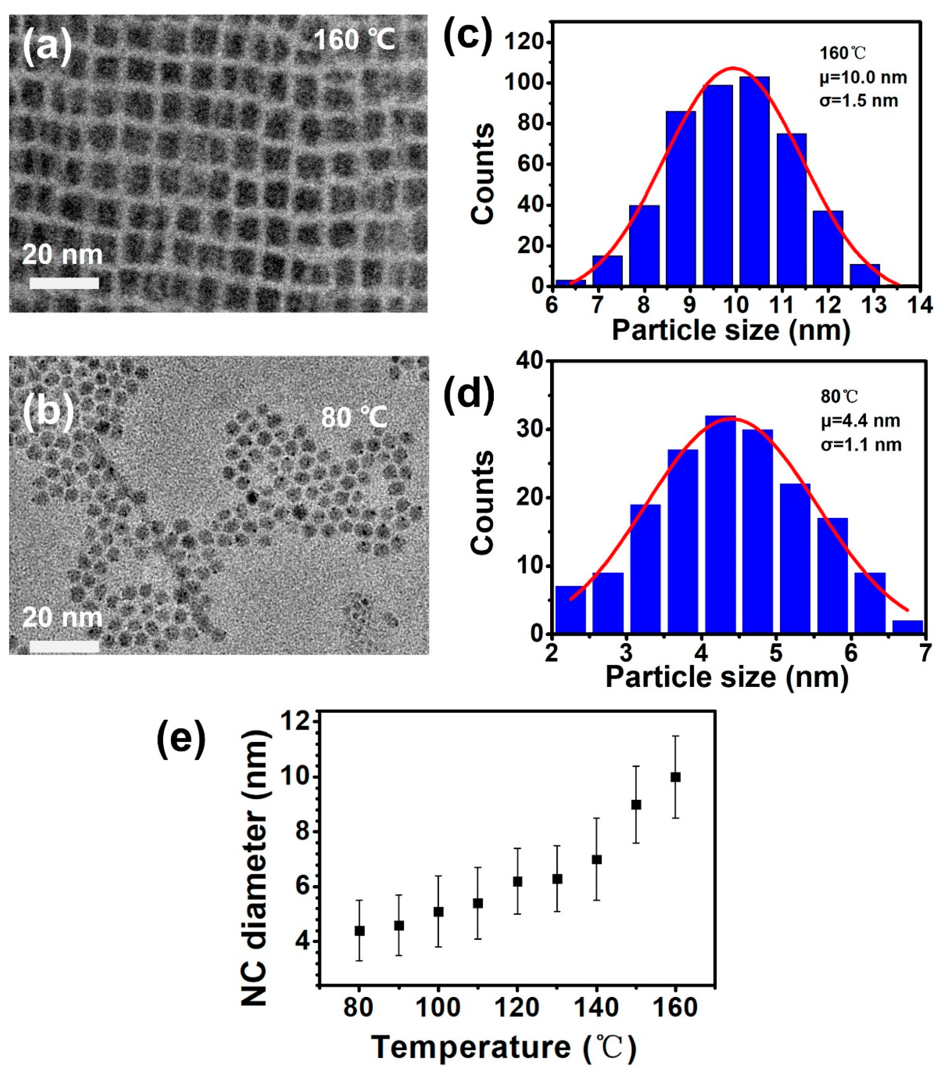
According to the method described in the Materials and Methods section, a series of CsPbBr3 samples with different reaction temperatures (80–160 °C) were prepared. TEM was used to examine the morphology and the particle diameters of CsPbBr3 NCs as shown in Figure 1a,b. The prepared CsPbBr3 NCs at 160 °C showed quasi cubic shape with high monodispersity and formed self-assembled arrays. In contrast, CsPbBr3 NCs obtained at the lowest 80 °C showed more spherical shape with smaller sizes. This indicated the initial growth of CsPbBr3 was more spatially isotropic. The size distribution of the above NC samples was shown as in Figure 1c,d by counting a group of NC sizes from TEM images. The results turned out that sizes of both kinds of NCs accorded Gaussian distribution. The diameter distribution of NC is 10.0 ± 1.5 nm for the sample fabricated at 160 °C and 4.4 ± 1.1 nm for the sample fabricated at 80 °C. More systematic investigation revealed that the obtained NCs with reaction temperature between 80 °C and 160 °C resulted in NC size in the range of 4.4–10.0 nm, which increased with raised temperature, as shown in Figure 1e.
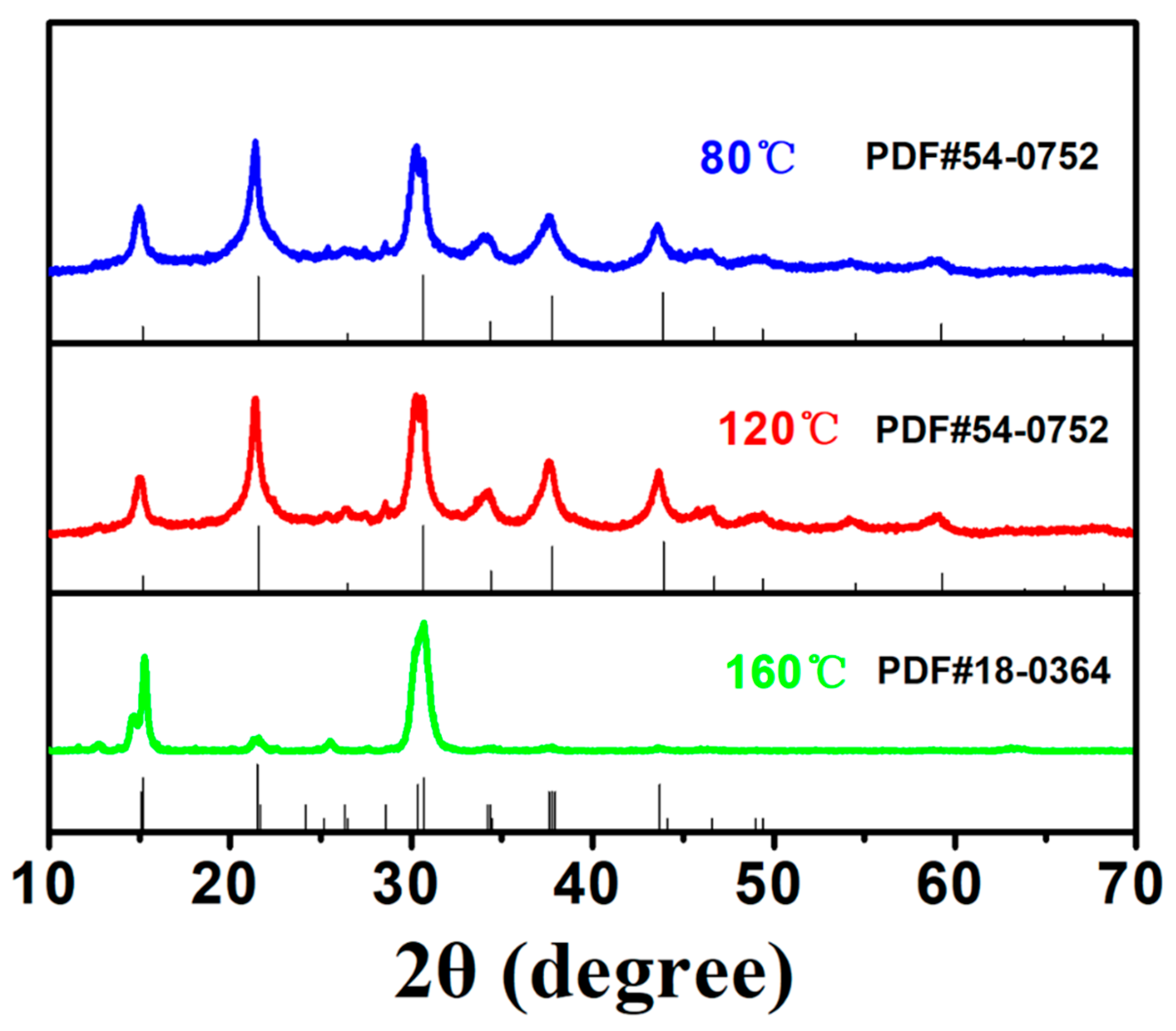
Then, XRD patterns were used to examine the crystalline structures of synthesized CsPbBr3 NCs with different reaction temperature. As shown in Figure 2, the XRD patterns of samples synthesized at 80 °C and 120 °C were both ascribable to typical cubic phase perovskite crystals (PDF#54-0752) without any other miscellaneous phase. It is already known that bulk CsPbBr3 single crystals require a crystalline temperature above 200 °C. Therefore, here the extra low forming temperature of CsPbBr3 NCs may originate from the surface effect of extra small particles as that large surface energy reduces the crystalline temperature for the cubic phase. Furthermore, it was found that further increasing the reaction temperature up to 160 °C led to slight changes in crystalline structures as it became a monoclinic phase (PDF#18-0364) crystal. This result indicated that overhigh reaction temperature led to the lattice distortion; in other words, the backbone of corner sharing [PbCl3] octahedra slightly tilts toward certain directions in high temperature conditions.
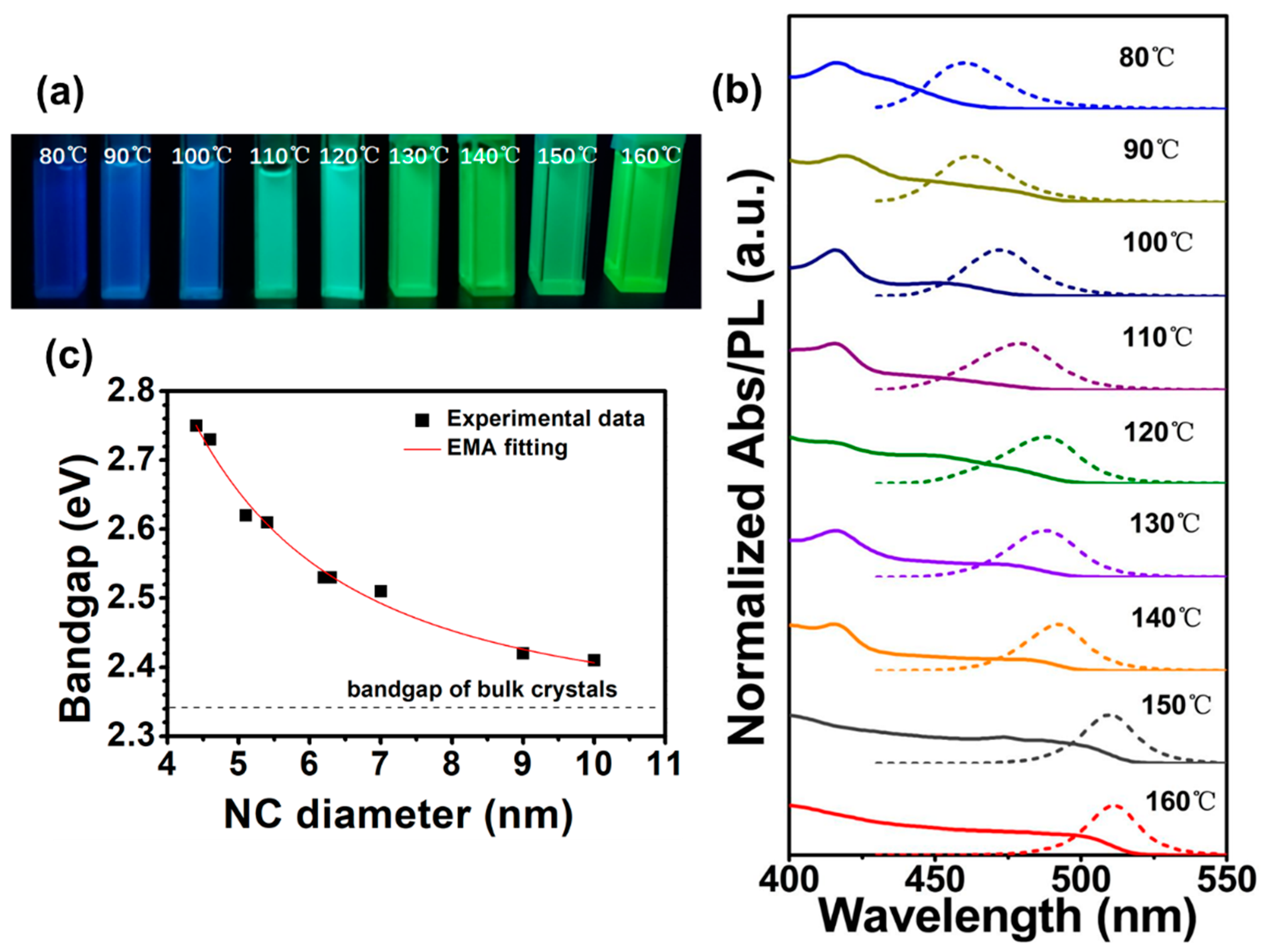
The purpose of controlling the CsPbBr3 NC sizes is to adjust their optoelectronic properties, especially to continuously adjust their absorption and emission wavelengths. Here, these properties were examined by UV-Vis and PL spectroscopies in our samples. Firstly, as shown in Figure 3a, under 296 nm irradiation of a UV lamp, the CsPbBr3 NC samples showed continuously changing emission color from bright green to dark blue following the decrease of reaction temperature from 160 °C to 80 °C. Under optical conditions, The PLQY results turned out to be 80–90%, which were found to weakly depend on NC sizes. Obviously, the PLQY of samples with blue emission (80–100 °C) possessed much higher PLQYs than CsPbCl3 or CsPbCl3–xBrx NCs. Their exact emission peaks excited by 375 nm laser were shown in Figure 3b for quantitative analysis. The peak wavelength was found blueshifting from 510 nm to 460 nm with shrinking NC sizes. Meanwhile, the full width at half maximum (FWHM) was found enlarged following the blueshifting peak position. For instance, the FWHM for NCs synthesized at 160 °C, 120 °C and 80 °C were 22 nm, 31 nm and 50 nm, respectively. This result indicated that as QCE appears, the bandgap of a single NC becomes more sensitive to its size. Thus, the overall width of emission peak tends to be more correlated to the size distribution of NCs compared to bulk crystals. Another explanation is that splitting of in-band energy levels leads to the in-band relaxation of carriers becoming forbidden; therefore, their recombination can continue via several split sub-energy levels, which leads to the broadening of emission peak.
Furthermore, the optical absorption band of the CsPbBr3 NCs was found blueshifting in the same manner of emission peak. Besides, an extra absorption peak at around 415 nm was also found after the reaction temperature was lower than 140 °C, whose peak position is fixed. This absorption peak fixed at the high energy side can be ascribed to the formation of 2D single-layered perovskite nanoplatelets [24]. By Tauc-plot analysis, the optical bandgaps of CsPbBr3 NCs were found well-matching with their peak energy. This result verifies the band-to-band transition behaviors stays dominant for the PL processes in NC samples, and their bandgaps broaden with reduced sizes. It has also been determined that the effective Bohr diameter of CsPbBr3 crystal is ~7 nm [8]. Here, the obtained NC diameters are close to or smaller than this value. Thus, the broadening of NC bandgaps can be estimated following EMA for 0D isotropic quantum dots as , in which represents the NC radius and represents the effective mass of excitons. As shown in Figure 3c, fitting result revealed that the broadening of bandgaps matched the EMA model well in the NC size range of 4–10 nm. This result indicated that the obtained CsPbBr3 NCs possessed 0D confinement structures with lengths in all three dimensions close to or smaller than the Bohr diameter, which is similar to the behaviors of nanocubes first reported by Protesescu and coworkers [8], instead of ones of layer-by-layer grown NPLs.
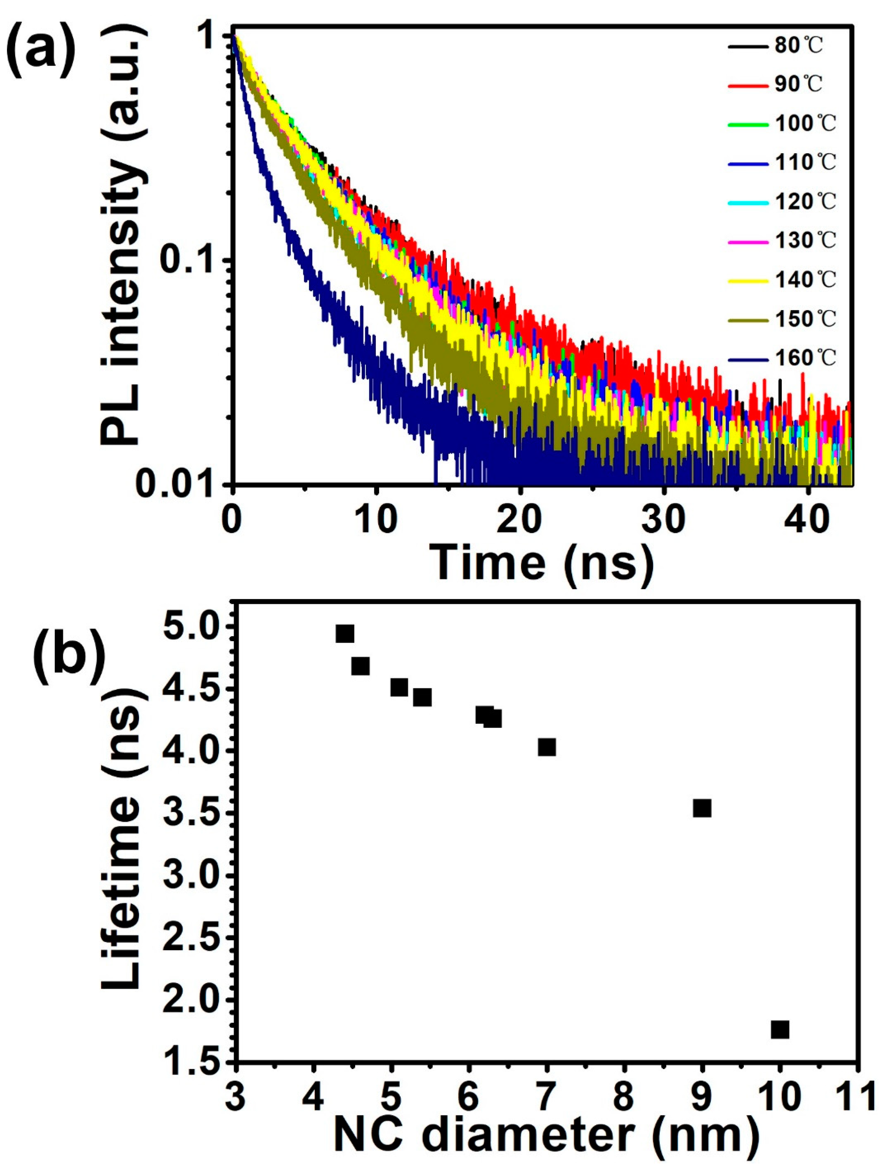
Although steady-state PL and absorption have shown clear signs of bandgap adjustments throughout size controls, QCE needs further verification throughout analysis of carrier dynamics mechanism in the system. As shown in Figure 4a, pumped by a 375 nm pulse laser and detected at their PL maximums, the PL intensities of CsPbBr3 NCs were found all decaying in periods of tens of nanoseconds, which agreed with the decay behaviors of intrinsic transitions found in bulk CsPbBr3 crystals. Interestingly, the PL decay seems to become slower with decreasing reaction temperature or NC size. Ordinarily, smaller size means larger surface defect density as well as a faster PL decay caused by shorter non-radiative recombination lifetime at room temperature. However, perovskites possess an inherent advantage as their defect tolerance factor: defects in CPNCs are benign to the electronic and optical properties, even being abundant, because defects in perovskites form states localizing within valence bands and conduction bands, or at worst, shallow states below conduction bands, so they do not form mid-gap trap states [25,26]. Therefore, the above result can be only explained as the increase of radiative recombination lifetime. By fitting the PL decay curves with single exponential decay function, the obtained PL lifetimes were summarized in Figure 4b for quantitative analysis. It turns out that PL lifetime monotonously increases following the shrinking of NC size, and there are two distinguishable periods of lifetime evolution: it raises quickly from 1.7 ns to 3.5 ns in the temperature range from 160 °C to 140 °C, at which the NC size decreased from 10 nm to 7 nm; then, it raises more steadily from 3.5 ns to 5 ns in the temperature range from 140 °C to 80 °C, at which the NC size decreased from 7 nm to 4.4 nm. Based on the above discussion, if the contribution of non-radiative recombination lifetime has been ruled out, the rapid change of radiative recombination lifetime may indicate a major change in radiative recombination pathway. Considering that Bohr diameter (~7 nm) is the threshold of weak confinement regime and strong confinement regime, this major change can be ascribed to the forming of Wannier–Mott excitons which have a longer radiative recombination lifetime than free electron–hole pairs. Meanwhile, the slow increase in PL lifetime in a strong confinement regime is due to the splitting of in-band energy level, which limits in-band relaxation of hot carriers.
By considering both the bandgap broadening that accords to the EMA model and exciton dynamics, we can confirm that the bandgap control is due to QCE. Furthermore, these results indicate the possibility of controlling the exciton dynamics, which provides the platform to investigate other beneficial effects such as MEG’s effect on the perovskite system. MEG requires an extra high energy level at least twice the bandgap to absorb incident photons, limited carrier relaxation rate within in-band energy level to prevent hot carrier cooling and relaxation of momentum conservation, which may be all fulfilled by QCE [27]. Thus, controlling QCE is one of the prerequisites of realizing MEG in CPNCs.
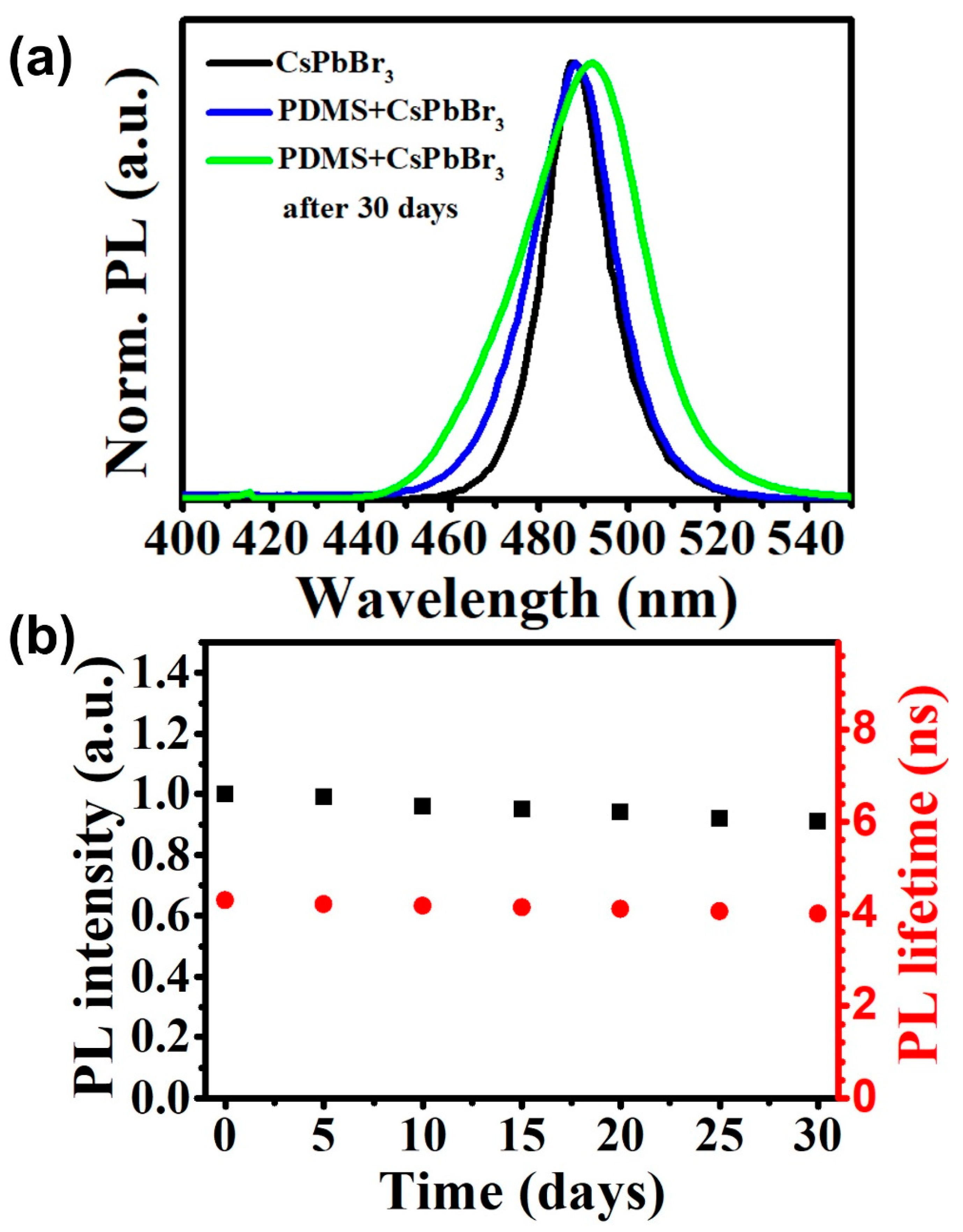
In practical applications of CsPbBr3 NCs, stability is a critical issue, for they easily deform if contacting polar solvent, moisture, oxygen or are exposed to UV light. There have been several surface-capping or encapsulation methods developed for solving these problems [28,29,30,31,32]. However, one difficulty is that most of these techniques may lead to the growth of NCs in the processes, which will vanish the QCE in the particles. In this work, we attempted to disperse and stabilize the as-prepared CsPbBr3 NCs in organic polymer PDMS matrix with maintaining their size distribution and optoelectronic properties. The final product can be made into functional slides, thin films or powders for several kinds of applications such as luminescent glass, photovoltaics or phosphors. As an example, the luminescent properties of the NC sample synthesized at 120 °C are shown as Figure 5a,b. By optimizing the synthesis process, the as-prepared stabilized NC sample in PDMS can be found with almost the same emission band with an expansion of FWHM less than 5 nm. This result indicates that the encapsulation process did not induce notable regrowth or aggregation of NCs. Then, the sample was put under an ambient condition for one month to examine the air and water stability. Its PL peak showed a redshift of 5 nm and a broadening of 10 nm. Its PL intensity and PL lifetime was continuously observed during the month. The PL intensity dropped only 10%, and the PL lifetime was found decreasing from 4.3 ns to 4.0 ns. These results indicate that the encapsulated sample showed outstanding resistance to oxygen and water.
4. Conclusions
In summary, CsPbBr3 NCs with 80–90% PLQYs were synthesized by a hot-injection method. The NC sizes were successfully tuned in the range of 4–10 nm by controlling reaction temperature at 80–160 °C. The absorption bands and emission peaks of these CsPbBr3 NCs were found blueshifting with decreasing NC size. There behaviors were ascribed to QCE, which induces the bandgap broadening following the EMA model for 0D isotropic quantum dots. The carrier dynamic investigation revealed that exciton recombination lifetime increased rapidly in the case that the NC diameter shrined below exciton Bohr diameter, which indicated the forming of Wannier–Mott excitons. Further decreasing of the NC diameter led to a slow raise of exciton lifetime, which was induced by stronger size confinement effect. This result indicated that the exciton lifetime was also controllable by shrinking of NC size.
Furthermore, the as-prepared CsPbBr3 NCs were dispersed and stabilized into PDMS matrix while maintaining their size distribution and optoelectronic properties. The encapsulated samples showed long-term air and water stability, which showed high potentials in optoelectronic applications.
Author Contributions
Conceptualization, T.L. and L.L.; formal analysis, T.L. and L.L.; investigation, K.Q. and X.B.; resources, T.L. and R.Z.; data curation, T.L., L.L. and K.Q.; writing—original draft preparation, T.L., K.Q. and L.L.; writing—review and editing, T.L. and L.L.; supervision, T.L.; project administration, T.L.; funding acquisition, T.L. All authors have read and agreed to the published version of the manuscript.
Funding
This research was funded by the National Natural Science Foundation of China (Grant Nos. 61504030, 11704081) and Guangxi Natural Science Foundation (2020GXNSFAA238043, 2020GXNSFAA297182, 2017GXNSFGA198005).
Conflicts of Interest
On behalf of all authors, the corresponding author states that there is no conflict of interest.
References
- Kojima, A.; Teshima, K.; Shirai, Y.; Miyasaka, T. Organometal Halide Perovskites as Visible-Light Sensitizers for Photovoltaic Cells. J. Am. Chem. Soc. 2009, 131, 6050–6051. [Google Scholar] [CrossRef]
- Correa-Baena, J.P.; Abate, A.; Saliba, M.; Tress, W.; Jesper, J.T.; Grätzel, M.; Hagfeldt, A. The rapid evolution of highly efficient perovskite solar cells. Energy Environ. Sci. 2017, 10, 710–727. [Google Scholar] [CrossRef]
- Lee, S.W.; Bae, S.; Kim, D.; Lee, H.S. Historical Analysis of High-Efficiency, Large-Area Solar Cells: Toward Upscaling of Perovskite Solar Cells. Adv. Mater. 2020, 32, 2002202. [Google Scholar] [CrossRef] [PubMed]
- Jeong, M.; Choi, I.W.; Go, E.M.; Cho, Y.; Kim, M.; Lee, B.; Jeong, S.; Jo, Y.; Choi, H.W.; Lee, J.; et al. Stable perovskite solar cells with efficiency exceeding 24.8% and 0.3-V voltage loss. Science 2020, 369, 1615. [Google Scholar] [CrossRef] [PubMed]
- Zhao, Y.; Zhu, K. Organic–inorganic hybrid lead halide perovskites for optoelectronic and electronic applications. Chem. Soc. Rev. 2016, 45, 655–689. [Google Scholar] [CrossRef] [PubMed]
- Hassan, Y.; Park, J.H.; Crawford, M.L.; Sadhanala, A.; Lee, J.; Sadighian, J.C.; Mosconi, E.; Shivanna, R.; Radicchi, E.; Jeong, M.; et al. Ligand-engineered bandgap stability in mixed-halide perovskite LEDs. Nature 2021, 591, 72–77. [Google Scholar] [CrossRef]
- Xu, J.; Li, X.; Xiong, J.; Yuan, C.; Semin, S.; Rasing, T.; Bu, X.H. Halide Perovskites for Nonlinear Optics. Adv. Mater. 2020, 32, 1806736. [Google Scholar] [CrossRef] [PubMed]
- Protesescu, L.; Yakunin, S.; Bodnarchuk, M.I.; Krieg, F.; Caputo, R.; Hendon, C.H.; Yang, R.X.; Walsh, A.; Kovalenko, M.V. Nanocrystals of Cesium Lead Halide Perovskites (CsPbX3, X = Cl, Br, and I): Novel Optoelectronic Materials Showing Bright Emission with Wide Color Gamut. Nano Lett. 2015, 15, 3692–3696. [Google Scholar] [CrossRef] [Green Version]
- Kovalenko, M.V.; Protesescu, L.; Bodnarchuk, M.I. Properties and potential optoelectronic applications of lead halide perovskite nanocrystals. Science 2017, 358, 745–750. [Google Scholar] [CrossRef] [Green Version]
- Akkerman, Q.A.; Rainò, G.; Kovalenko, M.V.; Manna, L. Genesis, challenges and opportunities for colloidal lead halide perovskite nanocrystals. Nat. Mater. 2018, 17, 394–405. [Google Scholar] [CrossRef] [PubMed]
- Li, X.; Wu, Y.; Zhang, S.; Cai, B.; Gu, Y.; Song, J.; Zeng, H. CsPbX3 Quantum Dots for Lighting and Displays: Room-Temperature Synthesis, Photoluminescence Superiorities, Underlying Origins and White Light-Emitting Diodes. Adv. Funct. Mater. 2016, 26, 2435–2445. [Google Scholar] [CrossRef]
- Kim, Y.H.; Kim, S.; Kakekhani, A.; Park, J.; Park, J.; Lee, Y.H.; Xu, H.; Nagane, S.; Wexler, R.B.; Kim, D.H.; et al. Comprehensive defect suppression in perovskite nanocrystals for high-efficiency light-emitting diodes. Nat. Photon. 2021, 15, 148–155. [Google Scholar] [CrossRef]
- Song, J.; Li, J.; Li, X.; Xu, L.; Dong, Y.; Zeng, H. Quantum Dot Light-Emitting Diodes Based on Inorganic Perovskite Cesium Lead Halides (CsPbX3). Adv. Mater. 2015, 27, 7162–7167. [Google Scholar] [CrossRef] [PubMed]
- Wang, H.; Zhang, P.; Zang, Z. High performance CsPbBr3 quantum dots photodetectors by using zinc oxide nanorods arrays as an electron-transport layer. Appl. Phys. Lett. 2020, 116, 162103. [Google Scholar] [CrossRef] [Green Version]
- Wang, Y.; Li, X.; Song, J.; Xiao, L.; Zeng, H.; Sun, H. All-Inorganic Colloidal Perovskite Quantum Dots: A New Class of Lasing Materials with Favorable Characteristics. Adv. Mater. 2015, 27, 7101–7108. [Google Scholar] [CrossRef]
- Zhang, F.; Zhong, H.; Chen, C.; Wu, X.G.; Hu, X.; Huang, H.; Han, J.; Zou, B.; Dong, Y. Brightly Luminescent and Color-Tunable Colloidal CH3NH3PbX3 (X = Br, I, Cl) Quantum Dots: Potential Alternatives for Display Technology. ACS Nano 2015, 9, 4533–4542. [Google Scholar] [CrossRef]
- Akkerman, Q.A.; D’Innocenzo, V.; Accornero, S.; Scarpellini, A.; Petrozza, A.; Prato, M.; Manna, L. Tuning the Optical Properties of Cesium Lead Halide Perovskite Nanocrystals by Anion Exchange Reactions. J. Am. Chem. Soc. 2015, 137, 10276–10281. [Google Scholar] [CrossRef] [Green Version]
- Brus, L. Electronic wave functions in semiconductor clusters: Experiment and theory. J. Phys. Chem. 1986, 90, 2555–2560. [Google Scholar] [CrossRef]
- Wilson, W.; Szajowski, P.; Brus, L. Quantum confinement in size-selected, surface-oxidized silicon nanocrystals. Science 1993, 262, 1242. [Google Scholar] [CrossRef]
- Alivisatos, A.P. Semiconductor Clusters, Nanocrystals, and Quantum Dots. Science 1996, 271, 933–937. [Google Scholar] [CrossRef] [Green Version]
- Smith, A.M.; Nie, S. Semiconductor Nanocrystals: Structure, Properties, and Band Gap Engineering. Acc. Chem. Res. 2010, 43, 190–200. [Google Scholar] [CrossRef] [Green Version]
- Wise, F.W. Lead Salt Quantum Dots: the Limit of Strong Quantum Confinement. Acc. Chem. Res. 2000, 33, 773–780. [Google Scholar] [CrossRef]
- Bekenstein, Y.; Koscher, B.A.; Eaton, S.W.; Yang, P.; Alivisatos, A.P. Highly Luminescent Colloidal Nanoplates of Perovskite Cesium Lead Halide and Their Oriented Assemblies. J. Am. Chem. Soc. 2015, 137, 16008–16011. [Google Scholar] [CrossRef] [PubMed] [Green Version]
- Akkerman, Q.A.; Motti, S.G.; Srimath Kandada, A.R.; Mosconi, E.; D’Innocenzo, V.; Bertoni, G.; Marras, S.; Kamino, B.A.; Miranda, L.; De Angelis, F.; et al. Solution Synthesis Approach to Colloidal Cesium Lead Halide Perovskite Nanoplatelets with Monolayer-Level Thickness Control. J. Am. Chem. Soc. 2016, 138, 1010–1016. [Google Scholar] [CrossRef] [PubMed] [Green Version]
- Huang, H.; Bodnarchuk, M.I.; Kershaw, S.V.; Kovalenko, M.V.; Rogach, A.L. Lead Halide Perovskite Nanocrystals in the Research Spotlight: Stability and Defect Tolerance. ACS Energy Lett. 2017, 2, 2071–2083. [Google Scholar] [CrossRef] [Green Version]
- Kang, J.; Wang, L.W. High Defect Tolerance in Lead Halide Perovskite CsPbBr3. J. Phys. Chem. Lett. 2017, 8, 489–493. [Google Scholar] [CrossRef] [PubMed]
- Ahumada-Lazo, R.; Saran, R.; Woolland, O.; Jia, Y.; Kyriazi, M.E.; Kanaras, A.G.; Binks, D.; Curry, R.J. Exciton effects in perovskite nanocrystals. J. Phys. Photonics 2021, 3, 021002. [Google Scholar] [CrossRef]
- Luo, B.; Naghadeh, S.B.; Zhang, J.Z. Lead Halide Perovskite Nanocrystals: Stability, Surface Passivation, and Structural Control. ChemNanoMat 2017, 3, 456–465. [Google Scholar] [CrossRef]
- Wang, H.; Lin, H.; Piao, X.; Tian, P.; Fang, M.; An, X.E.; Luo, C.; Qi, R.; Chen, Y.; Peng, H. Organometal halide perovskite nanocrystals embedded in silicone resins with bright luminescence and ultrastability. J. Mater. Chem. C 2017, 5, 12044–12049. [Google Scholar] [CrossRef]
- Wang, Y.; Zhu, Y.; Huang, J.; Cai, J.; Zhu, J.; Yang, X.; Shen, J.; Li, C. Perovskite quantum dots encapsulated in electrospun fiber membranes as multifunctional supersensitive sensors for biomolecules, metal ions and pH. Nanoscale Horiz. 2017, 2, 225–232. [Google Scholar] [CrossRef]
- Li, Z.J.; Hofman, E.; Li, J.; Davis, A.H.; Tung, C.H.; Wu, L.Z.; Zheng, W. Photoelectrochemically Active and Environmentally Stable CsPbBr3/TiO2 Core/Shell Nanocrystals. Adv. Funct. Mater. 2018, 28, 1704288. [Google Scholar]
- Sun, C.; Zhang, Y.; Ruan, C.; Yin, C.; Wang, X.; Wang, Y.; Yu, W.W. Efficient and Stable White LEDs with Silica-Coated Inorganic Perovskite Quantum Dots. Adv. Mater. 2016, 28, 10088–10094. [Google Scholar] [CrossRef] [PubMed]
Figure 1.
The TEM images of obtained CsPbBr3 NCs with reaction temperature of (a) 160 °C and (b) 80 °C. The distribution of NC sizes obtained by counting from the TEM images for CsPbBr3 NCs with reaction temperature of (c) 160 °C and (d) 80 °C. Red curves are the Gaussian fitting to the size data. (e) Reaction temperature dependency of the CsPbBr3 NCs diameter.

Figure 2.
XRD patterns of CsPbBr3 NCs with different reaction temperatures.

Figure 3.
(a) The appearance of as-prepared CsPbBr3 NCs with different reaction temperature, which were dissolved in n-hexane and irradiated by a 296 nm UV lamp in dark condition. (b) Absprtion spectra (solid lines) and emission spectra (dash lines) of CsPbBr3 NCs with different reaction temperature, in which the samples were excited by a 375 nm laser for emission spectrum measurements. (c) The relationship of NC diameters and their optical bandgaps obtained from absoption edges (dark blocks). Red curve shows the EMA fitting of experimental data.

Figure 4.
(a) PL decay curves of CsPbBr3 NCs with different reaction temperatures. (b) The relationship of NC diameters and their PL decay lifetimes, in which the PL lifetimes were obtained by fitting the PL decay curves with single exponential decay function.
Figure 4.
(a) PL decay curves of CsPbBr3 NCs with different reaction temperatures. (b) The relationship of NC diameters and their PL decay lifetimes, in which the PL lifetimes were obtained by fitting the PL decay curves with single exponential decay function.

Figure 5.
(a) Emission spectra for CsPbBr3 NCs synthesized at 120 °C with/without PDMS encapsulation and with exposing under ambient condition. The excitation wavelength is 375 nm. (b) Long-term stability of PL intensity and PL lifetime for CsPbBr3 NCs synthesized at 120 °C.
Figure 5.
(a) Emission spectra for CsPbBr3 NCs synthesized at 120 °C with/without PDMS encapsulation and with exposing under ambient condition. The excitation wavelength is 375 nm. (b) Long-term stability of PL intensity and PL lifetime for CsPbBr3 NCs synthesized at 120 °C.

Publisher’s Note: MDPI stays neutral with regard to jurisdictional claims in published maps and institutional affiliations. |
© 2021 by the authors. Licensee MDPI, Basel, Switzerland. This article is an open access article distributed under the terms and conditions of the Creative Commons Attribution (CC BY) license (https://creativecommons.org/licenses/by/4.0/).
Share and Cite
MDPI and ACS Style
Liao, L.; Quan, K.; Bin, X.; Zeng, R.; Lin, T. Bandgap and Carrier Dynamic Controls in CsPbBr3 Nanocrystals Encapsulated in Polydimethylsiloxane. Crystals 2021, 11, 1132. https://0-doi-org.brum.beds.ac.uk/10.3390/cryst11091132
AMA Style
Liao L, Quan K, Bin X, Zeng R, Lin T. Bandgap and Carrier Dynamic Controls in CsPbBr3 Nanocrystals Encapsulated in Polydimethylsiloxane. Crystals. 2021; 11(9):1132. https://0-doi-org.brum.beds.ac.uk/10.3390/cryst11091132
Chicago/Turabian StyleLiao, Lianxing, Kunhua Quan, Xiangshi Bin, Ruosheng Zeng, and Tao Lin. 2021. "Bandgap and Carrier Dynamic Controls in CsPbBr3 Nanocrystals Encapsulated in Polydimethylsiloxane" Crystals 11, no. 9: 1132. https://0-doi-org.brum.beds.ac.uk/10.3390/cryst11091132
Note that from the first issue of 2016, this journal uses article numbers instead of page numbers. See further details here.