
Fabrication and Evaluation of Low-Cost CrSi2 Thermoelectric Legs
by
 , , , , and
Sylvain Le Tonquesse
1,* ,
,
Yoshitaka Matsushita
2,
Priyanka Jood
3,
Michihiro Ohta
3,
Takao Mori
4 and
David Berthebaud
1,* 1
CNRS-Saint Gobain-NIMS, IRL 3629, Laboratory for Innovative Key Materials and Structures (LINK), National Institute for Materials Science (NIMS), Tsukuba 305-0044, Japan
2
National Institute for Materials Science (NIMS), 1-2-1 Sengen, Tsukuba 305-0047, Japan
3
Global Zero Emission Research Center, National Institute of Advanced Industrial Science and Technology (AIST), 16-1 Onogawa, Tsukuba 305-8569, Japan
4
National Institute for Materials Science (NIMS), MANA, 1-1-1 Namiki, Tsukuba 305-0044, Japan
*
Authors to whom correspondence should be addressed.
Crystals 2021, 11(9), 1140; https://0-doi-org.brum.beds.ac.uk/10.3390/cryst11091140
Submission received: 31 August 2021
/
Revised: 13 September 2021
/
Accepted: 15 September 2021
/
Published: 18 September 2021
(This article belongs to the Special Issue Thermoelectrics: from Materials to Devices)
Abstract
:CrSi is a promising thermoelectric material constituted of non-toxic and earth abundant elements that offer good perspectives for the mass production of inexpensive and reliable thermoelectric modules for waste heat recovery. Realization of robust metallic contacts with low electrical and thermal resistances on thermoelectric materials is crucial to maximize the conversion efficiency of such a device. In this article, the metallization of an undoped CrSi with Ti and Nb using a conventional Spark Plasma Sintering process is explored and discussed. These contact metals were selected because they have compatible thermal expansion coefficients with those of CrSi, which were determined in this study by X-ray Diffraction in the temperature range 299–899 K. Ti was found to be a promising contact metal offering both strong adhesion on CrSi and negligible electrical contact resistance (<1 cm). However, metallization with Nb resulted in the formation of cracks caused by large internal stress inside the sample during the fabrication process and the diffusion of Si in the metallic layer. A maximum conversion efficiency of 0.3% was measured for a sandwiched Ti/CrSi/Ti thermoelectric leg placed inside a thermal gradient of 427 K. The preliminary results obtained and discussed in this article on a relatively simple case study aim to initiate the development of more reliable and efficient CrSi thermoelectric legs with an optimized design.
1. Introduction
Thermoelectric (TE) generators are all-solid-state and greenhouse gas emission-free devices that enable the direct conversion of heat into electricity via the Seebeck effect. The most common architecture of TE modules consists of an assembly of n- and p-type TE materials connected electrically in series and thermally in parallel, sandwiched between two ceramic plates. The conversion efficiency is a monotonically increasing function of the figure of merit ZT = T/ of the TE materials where is the Seebeck coefficient, the electrical resistivity, the thermal conductivity, and T the temperature. However, the efficiency of current commercial TE modules composed of state-of-the-art materials with 1 remains below ≈8% which strongly limits their use to niche applications [1,2]. With the aim to increase the applicability of this technology, many attempts to improve the overall performance of TE modules have been reported recently in the literature and consist of using newly developed materials with an improved ZT [3,4,5,6,7], the development of alternative architectures [8,9,10,11,12,13], or fabrication process [14]. However, two important challenges remain: (i) the use of less toxic and expensive elements than those comprising the majority of current high-performance materials (Pb, Te, Bi…) and (ii) the realization of good-quality electrical contacts on TE materials that present low thermal and electrical contact resistances, strong mechanical resistance, and a good thermal stability.
Transition metal silicides such as CrSi[15], MnSi[16,17,18] or the low-temperature phase -FeSi[19] are composed of extremely inexpensive elements (<4 € kg) [20] and present good mechanical and oxidation resistance properties that makes them promising materials for the mass production of TE devices. Although this class of materials presents intrinsically good electronic properties, their ZT remains lower (<0.4) than the state-of-the-art materials due to relatively high thermal conductivities. In order to decrease , important research efforts leading to a significant improvement of the properties have been conducted recently mostly using strategies such as alloying [21], texturization [22], nanostructuration [23,24], or composite synthesis [25]. Despite the remarkable advances made on these materials, their integration into functional devices remains limited mostly because the realization of good-quality contacts is challenging and, thus, not well documented in the literature. Among the TE silicides, the p-type material CrSi (undoped ZT≈ 0.1, Ge-doped ZT≈ 0.25 [15]) is particularly interesting because it can be assembled with n-type -FeSi (co-doped ZT≈ 0.2 [26]) to make highly reliable, robust, and inexpensive modules.
In this article, we investigate the realization of metallic contacts on CrSi for the first time to our knowledge. The high temperature behavior of CrSi was first studied by XRD (X-ray Diffraction) from 299 to 899 K and the thermal expansion coefficients were determined. Two promising metals, Ti and Nb, were selected as contact materials as they have compatible thermal expansion behaviors and they are non-toxic and relatively earth-abundant elements. Two sandwiched TE legs Nb/CrSi/Nb and Ti/CrSi/Ti were synthesized from powders by a Spark Plasma Sintering (SPS) process and the resulting microstructure of the interfaces was analyzed by Scanning Electron Microscopy (SEM) and Energy Dispersive Spectroscopy (EDS) techniques. Finally, the electric contact resistance and the TE conversion efficiency of the Ti/CrSi/Ti leg were measured and future directions of development are discussed.
2. Materials and Methods
2.1. Material Synthesis
CrSi was synthesized by arc-melting Cr chips (Aldrich Chemicals, 99.995%) and Si pieces (Aldrich Chemicals, 99.95%) together in stoichiometric amounts. In order to ensure good homogenization, the ingot was remelted several times. The weight loss was kept under 0.2 wt.%. The obtained CrSi ingot was then pulverized into powder by ball-milling using a Fritsch Pulverisette 7 for 4 h at 200 rpm. SPS-sintered pellets were prepared at 1473 K for 10 min with an uni-axial pressure of 50 MPa in a graphite die using a Dr. Sinter Lab. Jr. SPS-322Lx apparatus.
2.2. High Temperature XRD Analysis
High temperature powder XRD was realized using a – Rigaku SmartLab diffractometer equipped with a Cu rotating target, a Ge(111) monochromator set at incident beam side selecting the Cu K radiation (1.54056 Å) and a D/teX Ultra 250 detector. The measurements were performed from 20 to 100 with a step width of 0.020 using variable slits. High-temperature measurements were performed from 299 K to 899 K every 50 K under Ar gas flow condition (1.0 L min). The X-ray powder patterns were fitted using the MAUD software [27,28]. The peak shapes were modeled using Thompson–Cox–Hastings pseudo-Voigt functions [29].
2.3. Thermoelectric Leg Fabrication and Characterization
The realization of electrical contact on CrSi was performed using Ti powder (Aldrich Chemicals, 99.7%, 100 mesh) or Nb powder (GoodFellow, 99.95%, maximum particle size of 74 m). For this, layers of metal powder (0.3 g for Nb, 0.2 g for Ti), of ball-milled CrSi (2 g) and again of metal powder (0.3 g for Nb, 0.2 g for Ti) were successively place on top of each other and cold pressed at 4 kN in a graphite die. The whole was then sintered using the conditions already given above. The SEM back-scattered electron image of the metal–thermoelectric junctions were obtained using a Hitachi Tabletop Microscope TM3000 with an acceleration voltage of 15 kV.
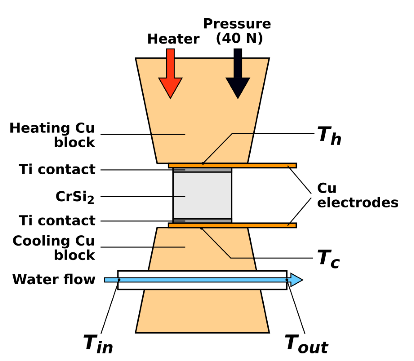
Scanning resistance measurement across the Ti/CrSi/Ti leg was realized using a home-made apparatus whose working principle was explained by Mengali et al. [30]. For performance characterization, the sample was cut in a rectangular shape with cross-section area of 0.60 cm × 0.60 cm = 0.36 cm and thickness of 0.49 cm. The open-circuit voltage (), total resistance (R), output power (), output heat flow (), and the maximum conversion efficiency () of the Ti/CrSi/Ti leg were measured under vacuum condition using an ULVAC Mini-PEM (full nomenclature of the symbols used in this article are shown in Table A1). A scheme of the set-up is shown in Figure 1 and is explained in more details in ref. [31]. The hot-side temperature of the leg varied from 320 K to 750 K using an electric heater, while the cold-side temperature was maintained at between 295 K and 307 K using water cooling. Cu foils on both sides of the sample were used as electrodes for electric measurement. In order to prevent large contact thermal resistance, the sample was pressed between two Cu blocks with an applied pressure of 40 N. For each temperature, the maximum power output was determined from the V-I plot. The ratio between the maximum output electrical power delivered to the load and the absorbed heat () at the hot-side was defined as the efficiency . Radiative and convective heat losses were considered as negligible, and was taken as the sum of and as given in relation (1).
In this work, was measured using the relation (2):
where and correspond to the water temperature before entering and after leaving the Cu heat sink, respectively, is the water flow and C is the specific heat of water. For each measured temperature, the measurement was performed with three different water flows of 0.5, 1 and 2 mL s and the average value was taken to calculate .
3. Results and Discussion
3.1. High Temperature X-ray Diffraction Study of CrSi
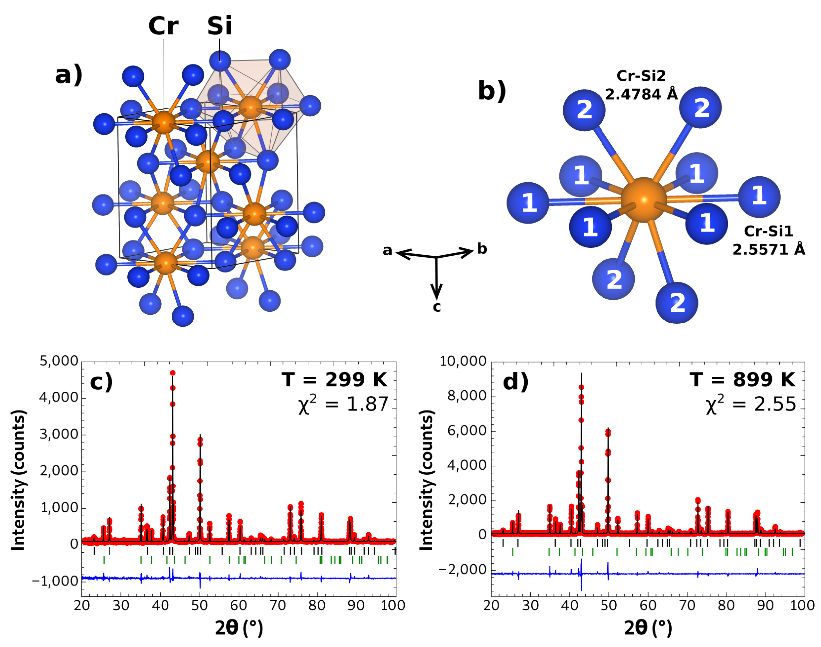
CrSi crystallized in the hexagonal C40 structure-type (P622, space group n 180) where the Cr atoms were located on the 3c Wyckoff sites (1/2, 0, 0) and the Si atoms on the 6i sites (x, , 1/3). The crystal structure of CrSi is shown in Figure 2a and can be described as a stacking of equivalent CrSi polyhedra connected by the faces. As shown in Figure 2b, the CrSi polyhedra were composed of six intralayer Si atoms (Si1) situated in the a–b plan and four interlayer Si (Si2) which formed a deformed tetrahedral. The Rietveld refined XRD pattern of CrSi powder after synthesis is shown in Figure 2c. All the peaks could be indexed with two phases, CrSi (88 wt.%) and alumina AlO (12 wt.%) that came from the sample holder. The refinement converged to the lattice parameters a = 4.42692(7) Å and c = 6.3729(2) Å that were in good agreement with literature values [32]. In this structure-type, an ideal c/a ratio of 1.5 resulted in the nearest ten intra- and interlayer Si to be at an equal distance of the central Cr atom [33]. The present c/a ratio of 1.439(1) resulted in six intralayer Cr–Si bonds being significantly longer (2.5571 Å) than the interlayer Cr–Si bonds (2.4784 Å). The refined positional parameter x = 0.166(1) for the Si atoms was close to the ideal value of 1/6 ≈ 0.1667 for which all six intralayer Cr–Si bonds had an identical length.
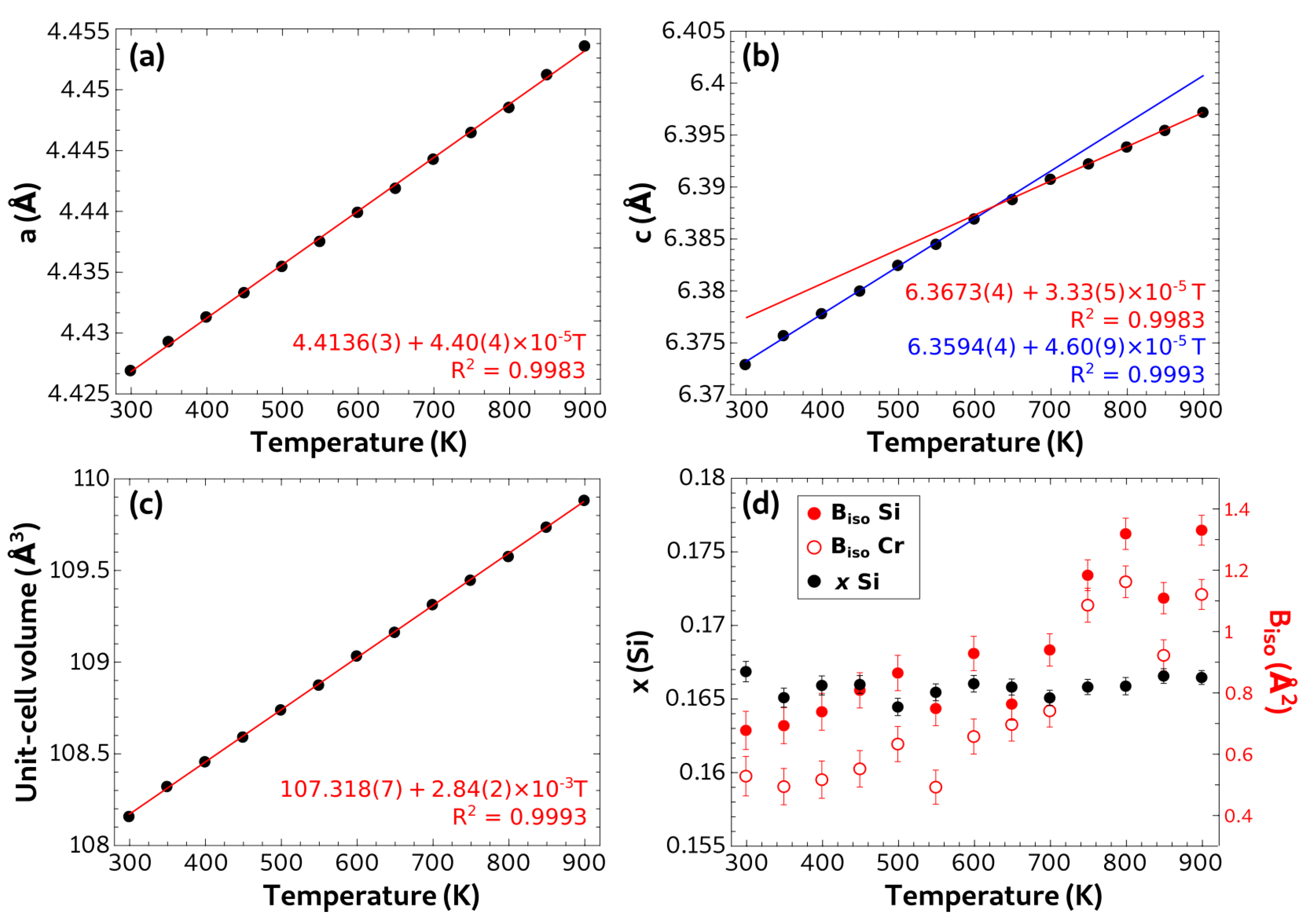
All the XRD patterns measured at temperature up to 899 K were fully indexed with the CrSi and AlO. After measurement and upon cooling, the structural parameter showed good reversibility and no trace of oxidation could be detected. The Rietveld refined XRD pattern at 899 K is shown in Figure 2d, while all the refined parameters and fit indexes (= /) are given in Table A2. The thermal evolution of the refined parameters a, c, x and are plotted in Figure 3. The thermal evolution of a was linear up to 899 K (Figure 3a) whereas it was only linear up to around 650 K for c (Figure 3b). Above this temperature, c entered a new linear regime characterized with a smaller slope coefficient of 3.3 × 10 Å K compared to 4.6 × 10 Å K below. Such a discontinuity was already reported at a similar temperature by T. Dasgupta et al. [34]. Despite this, the thermal evolution of the unit-cell volume was well fitted with a linear function up to 899 K (Figure 3c). Within the experimental uncertainties, the positional parameter x remained constant with an average value of 0.167 ± 7, meaning that all interlayer Cr–Si bond distances remained equivalent on the whole temperature range studied. As expected for conventional materials, globally increased with the temperature for both Cr and Si atoms.
The determination of the thermal evolution of the lattice parameters enabled the calculation of the coefficients of thermal expansion for each lattice direction () and lattice volume ( which had a high practical importance for the realization of electric contact. They were calculated at a temperature T using Formulae (3) and (4):
where L represents each one of the lattice parameters (a or c), V is the lattice volume, dL/dT and dV/dT are the slopes of the lattice parameters and volume thermal evolution, respectively. In the present case, the slopes were taken as from the best linear fits shown in Figure 3. Table 1 gives the different expansion coefficients calculated at 299 K and 899 K.
On the one hand, the thermal expansion coefficients of the a-axis and the lattice volume remained stable around 9.93(9) × 10 K and 26.2(2) × 10 K, respectively, on the whole temperature range studied. On the other hand, decreased significantly from 7.2(1) × 10 K to 5.21(8) × 10 K between 299 K and 899 K, respectively. The thermal expansion was significantly greater along the c-axis than the a-axis on the whole temperature range. This results in a constant decreased of the c/a ratio from 1.439(1) to 1.436(1) at 299 K and 899 K, respectively; another direct consequence in the faster elongation of the intralayer Cr–Si distances (2.5725 Å at 899 K, +0.6%) compared to the interlayer Cr–Si distances (2.4895 Å at 899 K, +0.3%). Using band-structure calculations, L. F. Mattheiss showed that decreasing the c/a ratio results in a shrinkage of the band-gap of CrSi[33]. The present results, therefore, supported the suggestion presented by T. Dasgupta et al. [34] that the rapid deterioration of the transport properties usually observed around 600 K of CrSi is partially due to the anisotropic thermal expansion of this material.
3.2. Fabrication of Ti and Nb Electric Contacts on CrSi
Matching the thermal expansion coefficient of the TE material and the contact metal was of utmost importance in order to avoid the cracking of the sample upon thermal treatment. For this work, Ti ( = 8.6 × 10 K) and Nb ( = 7.3 × 10 K) were selected to realize contacts on CrSi because they showed a relatively similar thermal expansion behavior [35]. Several different contact fabrication processes were reported in the literature for thermoelectrics such as sputtering [36], electroless plating [37], or thermal-spraying [38]. In the present work, the process simply consisted in placing the CrSi powder between two layers of metallic powder in the same graphite die and to densifying the whole together by SPS sintering. This method offered the advantages of being simple and reproducible, but also to enable a good adhesion of the contact metal on the TE material. A Ti/CrSi/Ti sample showing no visible cracks and presenting a good mechanical resistance was successfully synthesized using this process. However, the sample with Nb contacts cracked after the same thermal treatment and could not be handled without breaking. This may have originated from higher internal stress during the thermal treatment caused by the larger thermal expansion mismatch. Moreover, important interfacial diffusion and possible reactions at the interface also greatly influenced the mechanical resistance of the thermoelectric legs.
Figure 4 shows the microstructure of the contact regions (cross-section) for the two samples. Clear interfacial reaction layers were identified for both samples between the metal (light gray) and CrSi (dark gray). In the case of the Ti contact, Figure 4a,b shows the formation of a smooth and crack-free diffusion layer with an average thickness of about 8 m that was composed of two well separated phases. Going from CrSi to the Ti, the interfacial layers had Cr:Si:Ti chemical compositions of 35:47:18 and 5:46:49, which corresponded to the phases CrTiSi and (TiCr)Si, respectively. It should also be noted that Ti diffused significantly into CrSi as suggested by the chemical compositions of about TiCrSi, TiCrSi and TiCrSi determined at a distances of 5 m, 30 m, and 200 m away from the interface region, respectively. This was not surprising considering the high solubility of Ti in CrSi which can reach 70 at.% according to Karuppaiah et al. [39]. In the case of the sample with Nb contacts, Figure 4c,d show a thicker interface reaction region of 42 m. It was composed of multiple layers and presented cracks mostly on the Nb side. Going from CrSi to Nb, the different layers had Cr:Si:Nb chemical compositions of 45:50:5, 35:45:20, 5:60:35, and 5:36:59 which corresponded to the compounds (CrNb)Si, CrNbSi, (NbCr)Si, and (NbCr)Si, respectively. According to these EDS analyses, the Si atoms diffused into the Nb layer and CrSi formed between the CrSi and the Nb layer. The strain generated by the formation of Nb–Si based intermetallic inside the Nb metallic layer may explain the formation of cracks. EDS analyses inside the CrSi phase also revealed a slight diffusion of Nb into CrSi that rapidly fell below the detection limit of the technique at more than 40 m away from the interface region. The weaker diffusion of Nb compared to Ti in CrSi was consistent with literature data reporting a lower solubility limit of 10 at.% [40]. In the present case, Ti was, therefore, more adapted to the realization of mechanically resistant contacts on CrSi. However, the important migration of Ti atoms may have affected the electronic properties of CrSi and may, thus, necessitate the deposition of a diffusion barrier in future developments.
3.3. Electronic and Power Generation Characterization of the Ti/CrSi/Ti Leg
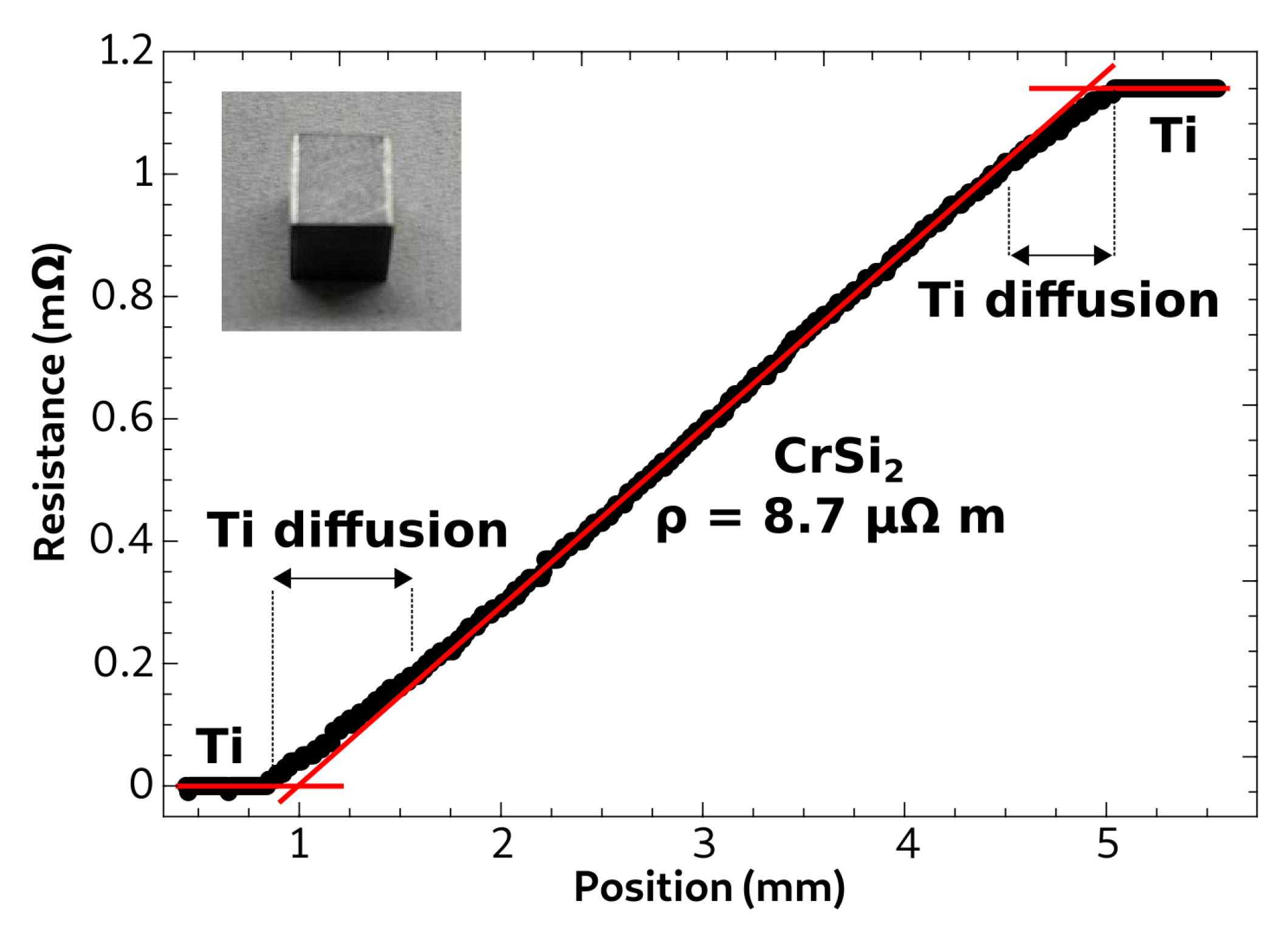
The electric contact resistance of the junction between the thermoelectric material and the metal layer is an important characteristic that should be minimized in order to increase its conversion efficiency. Figure 5 shows the evolution of the total resistance across the length of the Ti/CrSi/Ti leg at 298 K. The profile was characteristic of negligible contact resistance (<1 cm) as no visible jumps could be detected with this measurement resolution at the interfaces. The electrical resistivity of the TE material was estimated at 8.7 m from the slope of the linear section between 1.5 and 4.5 mm which was consistent with literature values around 10 m reported for CrSi[41]. However, it should be noted that the resistance profile started to deviate significantly from the linearity on both sides of the leg at a distance of about 500 m from the junctions. This was attributed to the diffusion of Ti inside CrSi, resulting in the formation of the solid solution TiCrSi clearly evidenced by SEM/EDS analyses. Ti is known to act as an efficient p-type dopant when substituting Cr in CrSi, which explains the local decrease of the electrical resistivity in those areas [39].
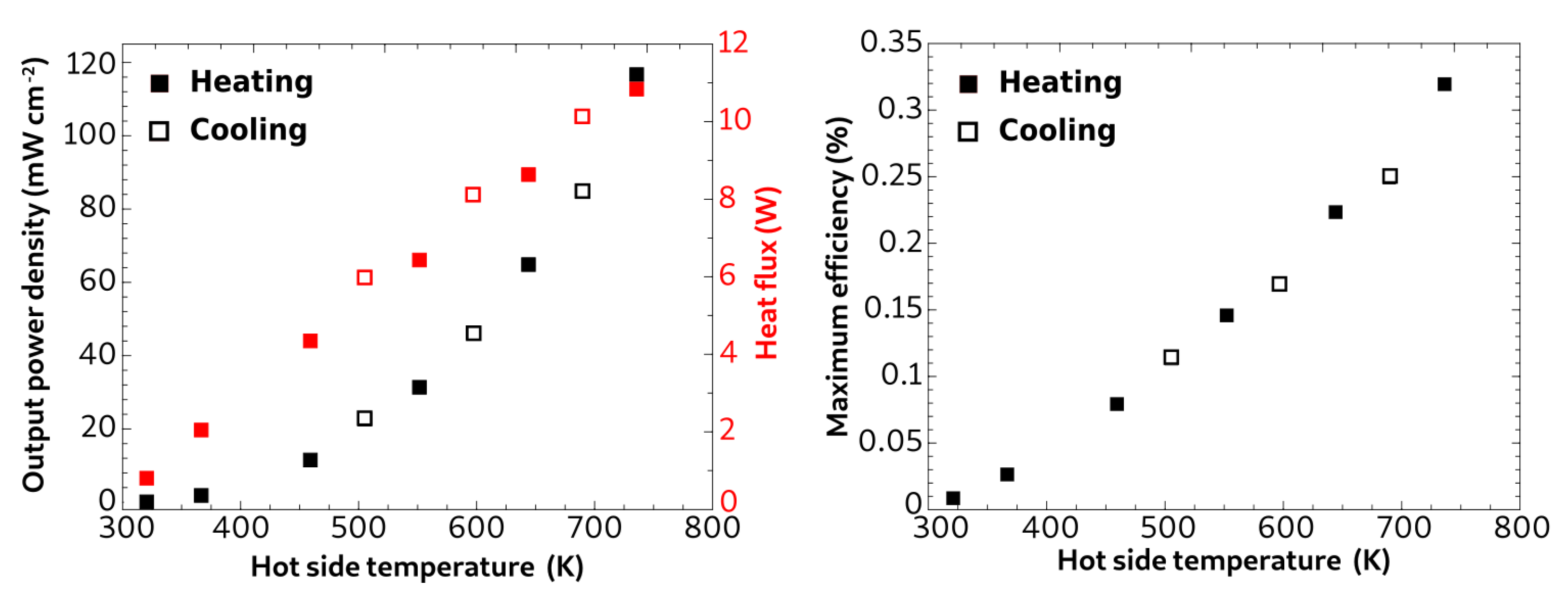
Figure 6a shows the maximum power output generated and the heat flux leaving the Ti/CrSi/Ti legs for different conditions. The filled and empty signs correspond to a measurement realized during the heating and cooling steps, respectively, showing the good reversibility of the measurement and, thus, the good thermal stability of the TE leg. logically increased with an increasing as a direct consequence of the voltage circuit () increase due to the Seebeck effect. The maximum value reached about 120 mW cm for a hot-side temperature of 736 K and of 427 K. Similarly, increasing results in a linear increase of going from 0.8 W to 11 W as the hot-side temperature increased from 327 K to 736 K. The measured values awee high compared to reported legs composed of optimized BiTe or PbTe because of the intrinsically higher thermal conductivity of pristine CrSi (>10 W m K compared to <4 W m K at 300 K). The doping or nanostructuration of CrSi should result in a significantly decreased and, thus, higher performances [15,23].
Table 2 gives the experimental , R, , and values measured for the present sample and the corresponding theoretical values expected for an ideal sample calculated using the relations:
where = 100 V K, = 10.0 m, and = 10.5 W m K are the Seebeck coefficient, the electrical resistivity, and thermal conductivity, respectively, of undoped CrSi at 298 K taken from [15,41], A is the cross-section area of the leg, d the length of the leg, = 736 K the hot-side temperature; = 309 K the cold-side temperature, and = 0.085 the figure of merit of CrSi at the average temperature = 522 K. It should be noted that relations (5) to (8) were based on the constant properties model, i.e., no variation of the TE properties with the temperature, which was not rigorously the case for CrSi[42]. However, in the present case, the low = 50 K made the variation of the properties negligible between the hot and cold sides and these relations were, thus, considered as acceptable models to predict , R, and . In the case of , the = 427 K was much larger and significant contributions from Joule and Thomson effects were expected to arise. Therefore, the calculated value of = 0.72 had to be considered with much care as it was, probably, largely overestimated.
Firstly, the calculated leg total resistance of 1.37 was close to the value of 1.15 measured by the scanning resistance measurement confirming the high-quality electrical contacts of this sample. The experimental resistance of 1.49 in Table 2 was significantly higher because it was measured using the two probe technique and, therefore, included the electrical contact resistances between the leg and the Cu electrodes. The experimentally measured of 3.95 V was 20% lower than the theoretical prediction of 5.50 V. This was attributed to (i) the diffusion of Ti in CrSi that was expected to lower the Seebeck coefficient of the materials locally and (ii) the non-negligible thermal resistance of the interfaces that decreased the effective to which the TE material was exposed. Indeed, the measured of 0.80 W was less than half of the calculated values of 1.97 W which confirmed that a high thermal contact resistance had to exist at the interface. However, it must be noted that the calculated value was overestimated because it did not take into account the thermal resistance between the TE leg and the Cu electrode. As a direct consequence, the experimental of 0.33% was lower by 60% compared to the theoretical (and overestimated) value of 0.72%. This conversion efficiency was relatively low compared to efficiencies of 3% and more reported for legs composed of BiTe or PbTe [7,43], which had higher ZT (≈1) than undoped CrSi (≈0.1). However, it should be recalled that the current leg was composed of low-cost and non-toxic material and that many optimizations of improvements remain to be investigated such as the use of nanostructured/doped CrSi with higher ZT, the deposition of a diffusion barrier to prevent Ti migration, or the optimization of the powders’ morphology to improve the contact thermal resistance.
4. Conclusions
In this paper, the realization of metal contact on the non toxic and inexpensive TE CrSi was reported, for the first time to our knowledge, using an SPS process. Ti and Nb were selected as contact metals as their thermal expansion coefficients matched closely those of CrSi, which were determined by a preliminary XRD analysis as = 9.93(9) × 10 K, = 7.2(1) × 10 K, and = 26.2(2) × 10 K at 299 K. Surprisingly, the c-axis thermal expansion was found to deviate from linearity at a temperature of about 627 K, resulting in a drop of reaching 5.21(8) × 10 K at 899 K. After the sintering treatment at 1473 K, a sandwiched Ti/CrSi/Ti TE leg was synthesized which showed limited diffusion at the interface and a good mechanical resistance. In comparison, the Nb/CrSi/Nb leg showed numerous cracks and broke after the same thermal treatment. This was attributed to the appearance of internal stresses in the sample during the cooling step caused by a larger thermal expansion mismatch between the different layer as well as a significant diffusion of Si-atoms in the Nb at the interface. Scanning electronic resistivity measurements on the Ti/CrSi/Ti leg showed a low contact resistance (<1 cm). A maximum conversion efficiency of 0.33% was measured for this sample when placed inside a thermal difference of 427 K. Despite the moderate efficiency, this study demonstrated that it is possible to make mechanically and chemically stable good-quality metallic contacts on CrSi using an inexpensive material and relatively simple processing methods. Finally, the present results laid the groundwork for the realization of more efficient TE legs composed of doped CrSi and with a more complex architecture, including a diffusion barrier to limit the migration of the metal atoms into the material.
Author Contributions
Conceptualization, S.L.T. and D.B.; methodology, S.L.T.; software, S.L.T.; validation, S.L.T. and Y.M.; formal analysis, S.L.T., Y.M. and P.J.; investigation, S.L.T., Y.M. and P.J.; resources, Y.M., M.O., T.M. and D.B.; data curation, S.L.T.; writing—original draft preparation, S.L.T.; writing—review and editing, Y.M., P.J., M.O., T.M. and D.B.; visualization, S.L.T.; supervision, D.B.; project administration, D.B.; funding acquisition, T.M. and D.B. All authors have read and agreed to the published version of the manuscript.
Funding
SLT and DB acknowledges ANR for the funding ANR-18-CE05-0037. YM acknowledges the funding from KAKENHI 19H05819. TM acknowledges the funding from JSPS KAKENHI JP19H00833 and JST-Mirai JPMJMI19A1.
Conflicts of Interest
The authors declare no conflict of interest.
Abbreviations
The following abbreviations are used in this manuscript:
| TE | Thermoelectric |
| XRD | X-ray Diffraction |
| SEM | Scanning Electron Microscopy |
| EDS | Energy Dispersive Spectroscopy |
| SPS | Spark Plasma Sintering |
Appendix A

Table A1.
Nomenclature of the symbols used in the article.
| Symbols | Meaning |
|---|---|
| Seebeck coefficient of the material | |
| Electrical resistivity of the material | |
| Thermal conductivity of the material | |
| Open-circuit voltage | |
| R | Total leg resistance |
| Electrical output power | |
| Input heat flow | |
| Output heat flow | |
| Input water temperature | |
| Output water temperature | |
| Water flow | |
| C | Specific heat of water |
| Conversion efficiency of the leg | |
| Thermal gradient applied to the leg | |
| Average temperature of the leg when placed inside a thermal gradient |
Table A2.
Rietveld refined lattice and structural parameters for CrSi at 299 K, 349 K, 399 K, 449 K, 499 K, 549 K, 599 K, 649 K, 799 K, 849 K, and 899 K.
Table A2.
Rietveld refined lattice and structural parameters for CrSi at 299 K, 349 K, 399 K, 449 K, 499 K, 549 K, 599 K, 649 K, 799 K, 849 K, and 899 K.
| 299 K | 349 K | 399 K | 449 K | 499 K | 549 K | 599 K | 549 K | 699 K | 749 K | 799 K | 849 K | 899 K | |
|---|---|---|---|---|---|---|---|---|---|---|---|---|---|
| a (Å) | 4.42692(7) | 4.42930(6) | 4.43132(6) | 4.43332(9) | 4.43548(7) | 4.4375(1) | 4.4399(1) | 4.44190(7) | 4.4443(1) | 4.44648(6) | 4.4485(1) | 4.4512(1) | 4.45359(9) |
| c (Å) | 6.3729(1) | 6.3757(1) | 6.3778(2) | 6.3800(1) | 6.3824(1) | 6.3845(2) | 6.3869(2) | 6.3888(1) | 6.3907(2) | 6.3922(1) | 6.3938(1) | 6.3954(2) | 6.3972(2) |
| V (Å) | 108.158(6) | 108.322(5) | 108.456(7) | 108.591(5) | 108.739(5) | 108.87(1) | 109.03(1) | 109.163(1) | 109.31(1) | 109.447(5) | 109.576(8) | 109.736(9) | 109.882(7) |
| Cr at 1/2, 0, 0 (Wickoff pos. 3c) | |||||||||||||
| (Å) | 0.53(6) | 0.49(6) | 0.52(6) | 0.55(6) | 0.63(6) | 0.49(5) | 0.66(5) | 0.70(5) | 0.74(6) | 1.09(5) | 1.16(5) | 0.92(5) | 1.12(5) |
| Si at x, , 1/3 (Wickoff pos. 6i) | |||||||||||||
| x | 0.167(1) | 0.165(1) | 0.166(1) | 0.1660(9) | 0.1644(9) | 0.1654(8) | 0.1660(9) | 0.166(1) | 0.1651(7) | 0.1658(6) | 0.1659(8) | 0.1665(7) | 0.1665(6) |
| (Å) | 0.67(6) | 0.69(6) | 0.74(6) | 0.81(6) | 0.86(6) | 0.75(5) | 0.93(6) | 0.76(5) | 0.94(5) | 1.18(5) | 1.32(5) | 1.11(5) | 1.33(5) |
| 1.87 | 2.23 | 1.92 | 1.94 | 2.02 | 2.00 | 1.95 | 2.45 | 2.67 | 2.56 | 2.87 | 2.64 | 2.55 | |
References
- He, R.; Schierning, G.; Nielsch, K. Thermoelectric Devices: A Review of Devices, Architectures, and Contact Optimization. Adv. Mater. Technol. 2018, 3, 1700256. [Google Scholar] [CrossRef] [Green Version]
- Champier, D. Thermoelectric generators: A review of applications. Energy Convers. Manag. 2017, 140, 167–181. [Google Scholar] [CrossRef]
- Liu, Z.; Sato, N.; Gao, W.; Yubuta, K.; Kawamoto, N.; Mitome, M.; Kurashima, K.; Owada, Y.; Nagase, K.; Lee, C.H.; et al. Demonstration of ultrahigh thermoelectric efficiency of ≈7.3% in Mg3Sb2/MgAgSb module for low-temperature energy harvesting. Joule 2021, 5, 1196–1208. [Google Scholar] [CrossRef]
- Prado-Gonjal, J.; Phillips, M.; Vaqueiro, P.; Min, G.; Powell, A.V. Skutterudite Thermoelectric Modules with High Volume-Power-Density: Scalability and Reproducibility. ACS Appl. Energy Mater. 2018, 1, 6609–6618. [Google Scholar] [CrossRef]
- Bu, Z.; Zhang, X.; Shan, B.; Tang, J.; Liu, H.; Chen, Z.; Lin, S.; Li, W.; Pei, Y. Realizing a 14% single-leg thermoelectric efficiency in GeTe alloys. Sci. Adv. 2021, 7, eabf2738. [Google Scholar] [CrossRef] [PubMed]
- Qiu, P.; Mao, T.; Huang, Z.; Xia, X.; Liao, J.; Agne, M.T.; Gu, M.; Zhang, Q.; Ren, D.; Bai, S.; et al. High-Efficiency and Stable Thermoelectric Module Based on Liquid-Like Materials. Joule 2019, 3, 1538–1548. [Google Scholar] [CrossRef]
- Jood, P.; Ohta, M.; Yamamoto, A.; Kanatzidis, M.G. Excessively Doped PbTe with Ge-Induced Nanostructures Enables High-Efficiency Thermoelectric Modules. Joule 2018, 2, 1339–1355. [Google Scholar] [CrossRef] [Green Version]
- Chetty, R.; Nagase, K.; Aihara, M.; Jood, P.; Takazawa, H.; Ohta, M.; Yamamoto, A. Mechanically durable thermoelectric power generation module made of Ni-based alloy as a reference for reliable testing. Appl. Energy 2020, 260, 114443. [Google Scholar] [CrossRef]
- Thimont, Y.; LeBlanc, S. The impact of thermoelectric leg geometries on thermal resistance and power output. J. Appl. Phys. 2019, 126, 095101. [Google Scholar] [CrossRef] [Green Version]
- El Oualid, S.; Kogut, I.; Benyahia, M.; Geczi, E.; Kruck, U.; Kosior, F.; Masschelein, P.; Candolfi, C.; Dauscher, A.; Koenig, J.D.; et al. High Power Density Thermoelectric Generators with Skutterudites. Adv. Energy Mater. 2021, 11, 2100580. [Google Scholar] [CrossRef]
- Li, W.; Poudel, B.; Nozariasbmarz, A.; Sriramdas, R.; Zhu, H.; Kang, H.B.; Priya, S. Bismuth Telluride/Half-Heusler Segmented Thermoelectric Unicouple Modules Provide 12% Conversion Efficiency. Adv. Energy Mater. 2020, 10, 2001924. [Google Scholar] [CrossRef]
- Caballero-Calero, O.; Rull-Bravo, M.; Platzek, D.; Cárdenas, M.D.; Fernández, R.; Moure, A.; Fernández, J.F.; Martín-González, M. Tubular ring thermoelectric module for exhaust pipes: From Skutterudite nanopowders to the final device. Energy 2021, 234, 121223. [Google Scholar] [CrossRef]
- Liang, J.; Wang, T.; Qiu, P.; Yang, S.; Ming, C.; Chen, H.; Song, Q.; Zhao, K.; Wei, T.R.; Ren, D.; et al. Flexible thermoelectrics: From silver chalcogenides to full-inorganic devices. Energy Environ. Sci. 2019, 12, 2983–2990. [Google Scholar] [CrossRef]
- Nozariasbmarz, A.; Saparamadu, U.; Li, W.; Kang, H.B.; Dettor, C.; Zhu, H.; Poudel, B.; Priya, S. High-performance half-Heusler thermoelectric devices through direct bonding technique. J. Power Sources 2021, 493, 229695. [Google Scholar] [CrossRef]
- Nagai, H.; Takamatsu, T.; Iijima, Y.; Hayashi, K.; Miyazaki, Y. Effects of Ge substitution on thermoelectric properties of CrSi2. Jpn. J. Appl. Phys. 2016, 55, 111801. [Google Scholar] [CrossRef]
- Le Tonquesse, S.; Dorcet, V.; Joanny, L.; Demange, V.; Prestipino, C.; Guo, Q.; Berthebaud, D.; Mori, T.; Pasturel, M. Mesostructure—Thermoelectric properties relationships in VxMn1-xSi1.74 (x = 0, 0.04) Higher Manganese Silicides prepared by magnesiothermy. J. Alloys Compd. 2020, 816, 152577. [Google Scholar] [CrossRef]
- Le Tonquesse, S.; Joanny, L.; Guo, Q.; Elkaim, E.; Demange, V.; Berthebaud, D.; Mori, T.; Pasturel, M.; Prestipino, C. Influence of Stoichiometry and Aging at Operating Temperature on Thermoelectric Higher Manganese Silicides. Chem. Mater. 2020, 32, 10601–10609. [Google Scholar] [CrossRef]
- Guo, Q.; Zhang, W.; Liu, Z.; Fu, X.; Le Tonquesse, S.; Sato, N.; Son, H.W.; Shimamura, K.; Berthebaud, D.; Mori, T. Thermoelectric Performance of Cr Doped and Cr–Fe Double-Doped Higher Manganese Silicides with Adjusted Carrier Concentration and Significant Electron–Phonon Interaction. ACS Appl. Mater. Interfaces 2021, 13, 8574–8583. [Google Scholar] [CrossRef] [PubMed]
- Le Tonquesse, S.; Verastegui, Z.; Huynh, H.; Dorcet, V.; Guo, Q.; Demange, V.; Prestipino, C.; Berthebaud, D.; Mori, T.; Pasturel, M. Magnesioreduction Synthesis of Co-Doped β-FeSi2: Mechanism, Microstructure, and Improved Thermoelectric Properties. ACS Appl. Energy Mater. 2019, 12, 8525–8534. [Google Scholar] [CrossRef]
- LeBlanc, S.; Yee, S.K.; Scullin, M.L.; Dames, C.; Goodson, K.E. Material and manufacturing cost considerations for thermoelectrics. Renew. Sust. Energ. Rev. 2014, 84, 313–317. [Google Scholar] [CrossRef]
- Chen, X.; Zhou, J.; Goodenough, J.B.; Shi, L. Enhanced thermoelectric power factor of Re-substituted higher manganese silicides with small islands of MnSi secondary phase. J. Mater. Chem. C 2015, 3, 10500–10508. [Google Scholar] [CrossRef]
- Sadia, Y.; Aminov, Z.; Mogilyansky, D.; Gelbstein, Y. Texture anisotropy of higher manganese silicide following arc-melting and hot-pressing. Intermetallics 2016, 68, 71–77. [Google Scholar] [CrossRef]
- Khalil, M.; Moll, A.; Godfroy, M.; Letrouit-Lebranchu, A.; Villeroy, B.; Alleno, E.; Viennois, R.; Beaudhuin, M. Thermoelectric properties and stability of nanostructured chromium disilicide CrSi2. J. Appl. Phys. 2019, 126, 135103. [Google Scholar] [CrossRef]
- Moll, A.; Viennois, R.; Boehm, M.; Koza, M.M.; Sidis, Y.; Rouquette, J.; Laborde, S.; Debray, J.; Menaert, B.; Castellan, J.P.; et al. Anharmonicity and Effect of the Nanostructuring on the Lattice Dynamics of CrSi2. J. Phys. Chem. C 2021, 125, 14786–14796. [Google Scholar] [CrossRef]
- Norizan, M.N.; Miyazaki, Y.; Ohishi, Y.; Muta, H.; Kurosaki, K.; Yamanaka, S. The Nanometer-Sized Eutectic Structure of Si/CrSi2 Thermoelectric Materials Fabricated by Rapid Solidification. J. Electron. Mater. 2018, 47, 2330–2336. [Google Scholar] [CrossRef]
- He, Z.; Platzek, D.; Stiewe, C.; Chen, H.; Karpinski, G.; Müller, E. Thermoelectric properties of hot-pressed Al- and Co-doped iron disilicide materials. J. Alloys Compd. 2007, 438, 303–309. [Google Scholar] [CrossRef]
- Lutterotti, L.; Matthies, S.; Wenk, H.R. MAUD (Material Analysis Using Diffraction): A user friendly Java program for Rietveld Texture Analysis and more. In Proceedings of the Twelfth International Conference on Textures of Materials (ICOTOM-12), Montreal, QC, Canada, 9–13 August 1999; Volume 1, p. 1599. [Google Scholar] [CrossRef]
- Lutterotti, L.; Vasin, R.; Wenk, H.R. Rietveld texture analysis from synchrotron diffraction images. I. Calibration and basic analysis. Powder Diffr. 2014, 19, 76–84. [Google Scholar] [CrossRef] [Green Version]
- Thompson, P.; Cox, D.E.; Hastings, J.B. Rietveld refinement of Debye-Scherrer synchrotron X-ray data from Al2O3. J. Appl. Cryst. 1987, 20, 79–83. [Google Scholar] [CrossRef] [Green Version]
- Mengali, O.; Seiler, M. Contact resistance studies on thermoelectric materials. Adv. Energy Convers. 1962, 2, 59–68. [Google Scholar] [CrossRef]
- Hu, X.; Yamamotoa, A.; Ohta, M.; Nishiate, H. Measurement and simulation of thermoelectric efficiency for single leg. Rev. Sci. Instrum. 2015, 86, 045103. [Google Scholar] [CrossRef] [PubMed]
- Nishida, I. The crystal growth and thermoelectric properties of chromium disilicide. J. Mater. Sci. 1972, 7, 1119–1124. [Google Scholar] [CrossRef]
- Mattheiss, L.F. Calculated structural properties of CrSi2, MoSi2, and WSi2. Phys. Rev. B 1992, 45, 3252–3259. [Google Scholar] [CrossRef]
- Dasgupta, T.; Etourneau, J.; Chevalier, B.; Matar, S.F.; Umarji, A.M. Structural, thermal, and electrical properties of CrSi2. J. Appl. Phys. 2008, 103, 113516. [Google Scholar] [CrossRef]
- Oberg, E.; Jones, D.; Holbrook, L.; Ryffel, H. Machinery’s Handbook, 29th ed.; Industrial Press Inc.: New York, NY, USA, 2012; pp. 376–377. [Google Scholar]
- Feng, S.P.; Chang, Y.H.; Yang, J.; Poudel, B.; Yu, B.; Ren, Z.; Chen, G. Reliable contact fabrication on nanostructured Bi2Te3-based thermoelectric materials. Phys. Chem. Chem. Phys. 2013, 15, 6757–6762. [Google Scholar] [CrossRef]
- Nguyen, Y.N.; Kim, S.; Bae, S.H.; Son, I. Enhancement of bonding strength in BiTe-based thermoelectric modules by electroless nickel, electroless palladium, and immersion gold surface modification. Appl. Surf. Sci. 2021, 545, 149005. [Google Scholar] [CrossRef]
- Zhang, J.F.; Yang, K.; Deng, C.M.; Deng, C.G.; Lui, M.; Dai, M.J.; Zhou, K.S. Method for spray thick nickel coating on the surface of semiconductor. Chinese Patent CN 104357784 A, 26 November 2014. [Google Scholar]
- Karuppaiah, S.; Beaudhuin, M.; Viennois, R. Investigation on the thermoelectric properties of nanostructured. J. Solid State Chem. 2013, 199, 90–95. [Google Scholar] [CrossRef]
- Nagai, H.; Takamatsu, T.; Iijima, Y.; Hayashi, K.; Miyazaki, Y. Effects of Nb substitution on thermoelectric properties of CrSi2. J. Alloys Compd. 2016, 687, 37–41. [Google Scholar] [CrossRef]
- Nishida, I.; Sakata, T. Semiconducting properties of pure and Mn-doped chromium disilicides. J. Phys. Chem. Solids 1978, 39, 499–505. [Google Scholar] [CrossRef]
- Kim, H.S.; Liu, W.; Ren, Z. Advanced Thermoelectrics: Materials, Contacts, Devices, and Systems; CRC Press: Boca Raton, FL, USA, 2018; Chapter 13. [Google Scholar]
- Hu, X.; Nagase, K.; Jood, P.; Ohta, M.; Yamamoto, A. Power Generation Evaluated on a Bismuth Telluride Unicouple Module. J. Electron. Mater. 2015, 44, 1785–1790. [Google Scholar] [CrossRef]
Figure 1.
Scheme of the thermoelectric leg characterization set-up used in the present work (MiniPEM, ULVAC).
Figure 1.
Scheme of the thermoelectric leg characterization set-up used in the present work (MiniPEM, ULVAC).

Figure 2.
Scheme of the (a) crystal structure of CrSi and (b) coordination environment around Cr with six intralayer Si1 and four interlayer Si2 atoms. Rietveld refined XRD patterns of CrSi measured at (c) 299 K and at (d) 850 K. The experimental data were plotted in red symbols, the calculated pattern with a black line, and the difference with a blue line. The vertical ticks indicate the theoretical Bragg positions of CrSi (black) and AlO (green).

Figure 3.
Thermal evolution of the lattice parameters (a) a and (b) c, (c) the unit cell volume and (d) the positional parameter x in black and the global isotropic atomic displacement parameters B in red.
Figure 3.
Thermal evolution of the lattice parameters (a) a and (b) c, (c) the unit cell volume and (d) the positional parameter x in black and the global isotropic atomic displacement parameters B in red.

Figure 4.
SEM back-scattered images showing the microstructure of the contact interface after SPS sintering. The images (a,b) and (c,d) show the Ti–CrSi and the Nb–CrSi interfaces, respectively, at different magnifications. The chemical composition of the different phases was determined by EDS measurements.

Figure 5.
Scanning electrical resistance of the SPS Ti/CrSi/Ti legs. The picture in inset shows the leg used for the measurement.
Figure 5.
Scanning electrical resistance of the SPS Ti/CrSi/Ti legs. The picture in inset shows the leg used for the measurement.

Figure 6.
Experimental measurement of (a) the output power density (black) and the total heat flux (red) and (b) the maximum conversion efficiency measured of the Ti/CrSi/Ti thermoelectric leg. The filled and empty symbols correspond to the heating and cooling steps, respectively.
Figure 6.
Experimental measurement of (a) the output power density (black) and the total heat flux (red) and (b) the maximum conversion efficiency measured of the Ti/CrSi/Ti thermoelectric leg. The filled and empty symbols correspond to the heating and cooling steps, respectively.

Table 1.
Lattice and its volume thermal expansion coefficients of CrSi at 299 K and 899 K.
| 299 K | 899 K | |
|---|---|---|
| (× 10 K) | 9.93(9) | 9.88(9) |
| (× 10 K) | 7.2(1) | 5.21(8) |
| (× 10 K) | 26.2(2) | 25.8(2) |
Table 2.
Experimentally measured using MiniPEM and predicted , R, and at = 298 K, = 50 K, and at = 522 K, = 427 K.
Table 2.
Experimentally measured using MiniPEM and predicted , R, and at = 298 K, = 50 K, and at = 522 K, = 427 K.
| Measured | Calculated | |
|---|---|---|
| (mV) | 3.95 | 5.50 |
| R (m) | 1.49 | 1.35 |
| (W) | 0.85 | 1.97 |
| (%) | 0.33 | 0.72 |
Publisher’s Note: MDPI stays neutral with regard to jurisdictional claims in published maps and institutional affiliations. |
© 2021 by the authors. Licensee MDPI, Basel, Switzerland. This article is an open access article distributed under the terms and conditions of the Creative Commons Attribution (CC BY) license (https://creativecommons.org/licenses/by/4.0/).
Share and Cite
MDPI and ACS Style
Le Tonquesse, S.; Matsushita, Y.; Jood, P.; Ohta, M.; Mori, T.; Berthebaud, D. Fabrication and Evaluation of Low-Cost CrSi2 Thermoelectric Legs. Crystals 2021, 11, 1140. https://0-doi-org.brum.beds.ac.uk/10.3390/cryst11091140
AMA Style
Le Tonquesse S, Matsushita Y, Jood P, Ohta M, Mori T, Berthebaud D. Fabrication and Evaluation of Low-Cost CrSi2 Thermoelectric Legs. Crystals. 2021; 11(9):1140. https://0-doi-org.brum.beds.ac.uk/10.3390/cryst11091140
Chicago/Turabian StyleLe Tonquesse, Sylvain, Yoshitaka Matsushita, Priyanka Jood, Michihiro Ohta, Takao Mori, and David Berthebaud. 2021. "Fabrication and Evaluation of Low-Cost CrSi2 Thermoelectric Legs" Crystals 11, no. 9: 1140. https://0-doi-org.brum.beds.ac.uk/10.3390/cryst11091140
Note that from the first issue of 2016, this journal uses article numbers instead of page numbers. See further details here.