Article

Impact of Bias Temperature Instabilities on the Performance of Logic Inverter Circuits Using Different SiC Transistor Technologies

1
Institute for Microelectronics, TU Wien, Gusshausstrasse 27-29, 1040 Vienna, Austria
2
Christian Doppler Laboratory for Single-Defect Spectroscopy, Institute for Microelectronics, TU Wien, Gusshausstrasse 27-29, 1040 Vienna, Austria
*
Author to whom correspondence should be addressed.
Submission received: 17 August 2021 / Revised: 8 September 2021 / Accepted: 15 September 2021 / Published: 21 September 2021
(This article belongs to the Special Issue Robust Microelectronic Devices)

Abstract

:
All electronic devices, in this case, SiC MOS transistors, are exposed to aging mechanisms and variability issues, that can affect the performance and stable operation of circuits. To describe the behavior of the devices for circuit simulations, physical models which capture the degradation of the devices are required. Typically compact models based on closed-form mathematical expressions are often used for circuit analysis, however, such models are typically not very accurate. In this work, we make use of physical reliability models and apply them for aging simulations of pseudo-CMOS logic inverter circuits. The model employed is available via our reliability simulator Comphy and is calibrated to evaluate the impact of bias temperature instability (BTI) degradation phenomena on the inverter circuit’s performance made from commercial SiC power MOSFETs. Using Spice simulations, we extract the propagation delay time of inverter circuits, taking into account the threshold voltage drift of the transistors with stress time under DC and AC operating conditions. To achieve the highest level of accuracy for our evaluation we also consider the recovery of the devices during low bias phases of AC signals, which is often neglected in existing approaches. Based on the propagation delay time distribution, the importance of a suitable physical defect model to precisely analyze the circuit operation is discussed in this work too.

1. Introduction

Due to its outstanding properties, silicon carbide (SiC) is an excellent candidate for replacing conventional silicon-based power devices, especially for applications operating in harsh environments [1]. SiC MOSFETs offer a superior dynamic and thermal performance compared to traditional Silicon (Si) power MOSFETs. One key advantage of SiC as substrate material is that the achievable electric fields are around ten times higher than for their Si counterparts, which allows the design of MOSFETs with smaller on-resistance and smaller parasitic capacitance.
The features mentioned above for SiC MOSFETs have a positive impact, for instance, on the power dissipation for either lower or higher power levels [2] and play an essential role in the field of robust microelectronic devices. However, the performance of SiC MOSFETs is still below the theoretical limit of SiC, mainly due to the trapping of electrons in the channel region. Even though post-oxidation annealing has enabled the fabrication of high-quality SiC power transistors, the devices still suffer from a considerable number of imperfections at the semiconductor/insulator interface. The trapping of charge carriers at such defect states gives rise to a notable drift of the threshold voltage of SiC transistors, which is known as the bias temperature instability (BTI) [3,4]. As a consequence of BTI, an increase of V th during the operation of the device introduces additional delays in circuits.
Furthermore, this may also lead to a higher on-resistance which negatively affects the power conversion efficiency of selected circuits [3]. Thus, the reliability of circuits employing SiC devices needs to be studied very carefully, especially for applications where the stable device performance and the lifetime are critical [5]. A particular challenge for high-power devices is that the drift of the threshold voltage in return can lead to an increase of the losses in the transistor and cause and increase in the operating temperature of the system [6]. Thus, threshold voltage stability is an essential issue for power devices and applications. To optimize the performance and analyze the circuit behavior under certain operating conditions, circuit simulations employing Spice simulators are a beneficial tool. In Spice simulators accurate compact models are the key components to precisely reproduce the electrical behavior of either devices or circuits. In our work we employ both physical device simulations and circuit simulations to evaluate the behavior of logic inverter circuits using different device technologies.
In more detail, we make use of 2nd and 3rd generation of commercially available SiC power MOSFETs provided by Cree, specifically the devices are C2M0280120D and C3M0065090J, respectively. All device kinds are fabricated on SiC substrate, however, their behavior it terms of drift of the threshold voltage is different. This is due to the fact that each device has been fabricated under different processing conditions which leads to a different trap distribution. As a consequence, our reliability model has to be calibrated to each device variant, i.e., to each device technology, individually. In the following we will refer to C3M0065090J as T1 and C2M0280120D as T2 to better comprehend the results. We also used the SCT10N120 SiC power MOSFET from STMicroelectronics. Likewise, we will identify this device from now on as T3. The device vendors provide the respective spice models of the transistors [7,8], which we employ in our simulations. The models have been calibrated using static and dynamic measurements. However, these models typically do not account for aging mechanisms such as BTI. To close this gap, we evaluate the impact of BTI on the device behavior under operation, e.g., the drift of the threshold voltage over time. Furthermore, we combine the provided models with our calibrated reliability simulations to thoroughly analyze the degradation of the performance of the inverter circuits over time.

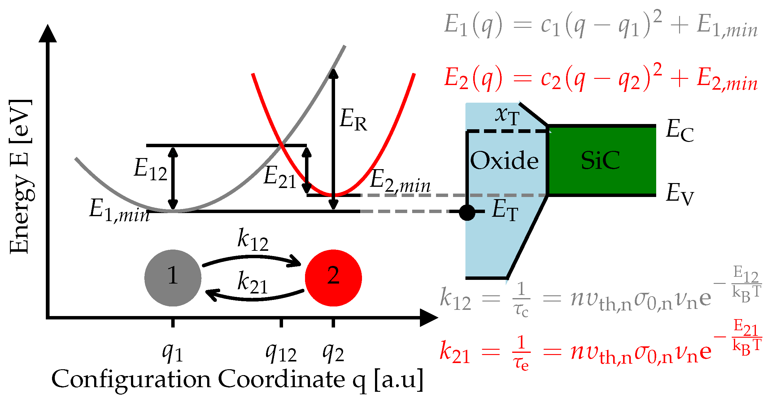
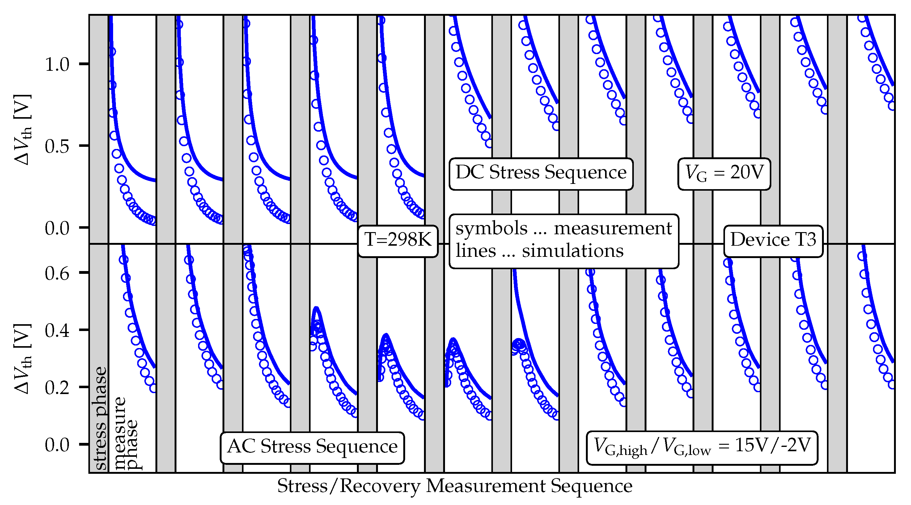
2. Charge Trapping and Model Calibration

One of the most prominent stability issues of devices is the so -called BTI. This aging mechanism has been extensively studied in the literature for Si/SiO2 [9,10,11,12], Si/HK [13,14,15,16] and SiC/SiO2 material systems [17]. BTI typically evolves as a drift of the threshold voltage with operation time and is characterized at higher gate voltages to accelerate V th degradation. The origin of the observed V th lies in charge trapping at interface traps and oxide defects [18,19].
Using measure-stress-measure (MSM) experiments [18], one can study this phenomenon as well as the creation of new defects. Typically power-law functions have been widely used to reproduce the threshold voltage drift V th with stress time. However, using power-law-like formulas can lead to an erroneous prediction of BTI’s impact on the device and circuit parameters. This simple formula does not account for the saturation of V th at high-stress times [19]. To ensure full accuracy in simulations, physical charge trapping models, for instance, the two-state defect model represented in Figure 1, should be preferably used [20,21]. This model is implemented in our open-source reliability simulator Comphy [21]. Our BTI simulator Comphy employs a two-state defect model based on the non-radiative multiphonon (NMP) theory. Moreover, it is used to calculate the charge capture and emission events at oxide defects to explain the V th . The most important parameters, as well as the expressions to determine the charge transitions times τ c and τ e , are shown in the configuration coordinate diagram in Figure 1. The principle idea of the model is that a charge carrier has to overcome the energy barrier depicted as E 12 and E 21 to change the charge state of a certain defect. In the semi-classical picture the barriers can be computed considering the intersection of the parabolas. Their relative position of the parabolas thereby depends on the applied gate bias and the energetic trap level of the defect. E 2 refers to the energy level of the carrier reservoir (e.g., conduction band edge or valence band edge), and E 1 describes the trap level of the defect. Other model parameters are the curvature of the parabolas c, the electron concentration n, the thermal velocity v th , n , the capture cross-section σ , and the tunneling coefficient ν .
Using Comphy the experimental data from various transistor technologies can be accurately reproduced. In [17,19] we make use of this model to precisely explain charge trapping at DC and AC operating conditions, as shown in Figure 2, for the technologies investigated in this work. It has to be noted that especially the saturation of the threshold voltage drift behavior can be nicely explained by this model [19].
The calibration of our reliability simulation tool is based on two types of experiments [19,22]: (i) DC-MSM sequences for different bias applied at room temperature, see Figure 3 (left), and (ii) AC-MSM measurements to characterize the operation of the transistors in switching applications, see Figure 3 (right). In the last case, a short AC stress during a time around 100 ms is applied repeatedly. At the last AC cycle of the signal, the stress is interrupted ( t AC , interrupt ). Then a V th recovery trace is extracted for a time equal to 10 ms considering a fixed I D = 1 mA through the channel of the device.
To ensure full accuracy of our simulation framework the tools are calibrated considering both DC and short-term AC experimental data to derive the surface potential from a given gate voltage, doping concentration in the channel, the oxide thickness and work function difference for each technology. As can be seen in Figure 4, Figure 5 and Figure 6, using our theoretical model can nicely replicate the device behavior for static and quasi-static operation conditions. This enables us now to look more detailed into the impact of BTI on different circuits.

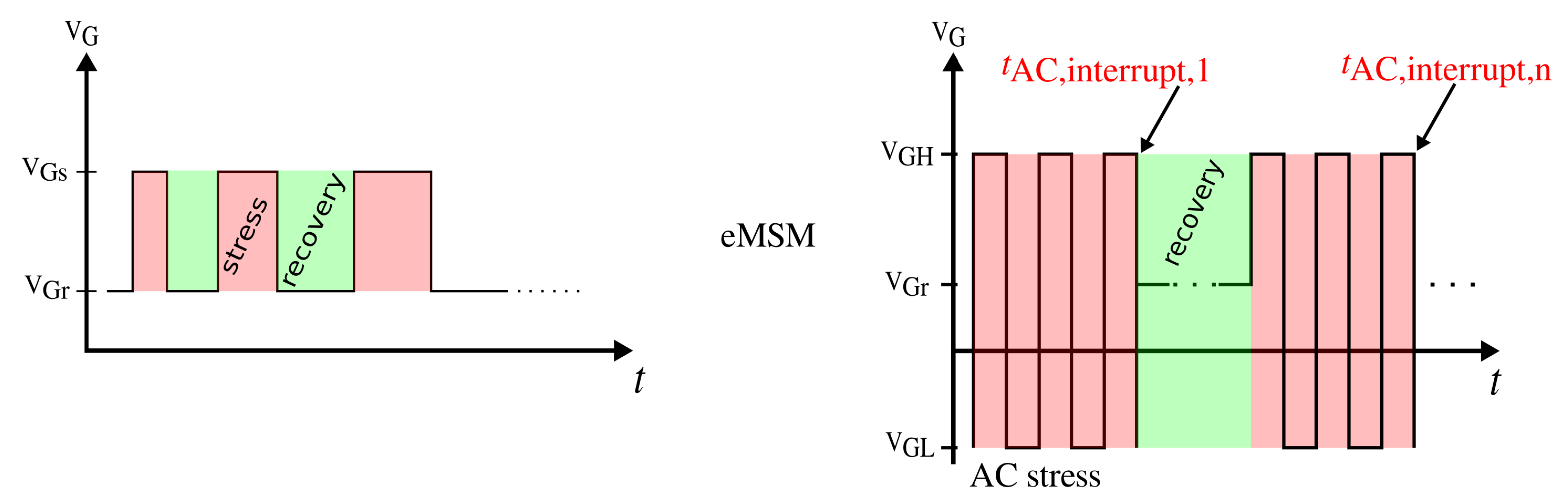
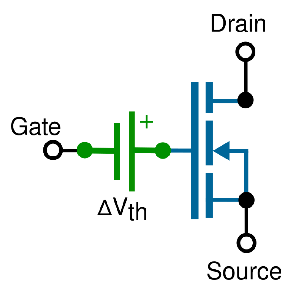
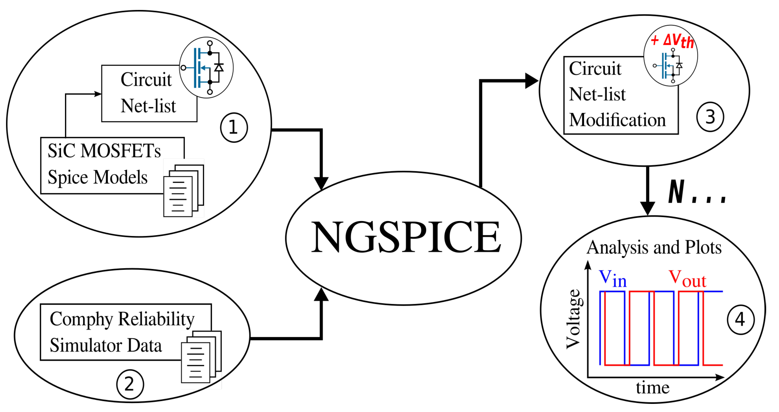
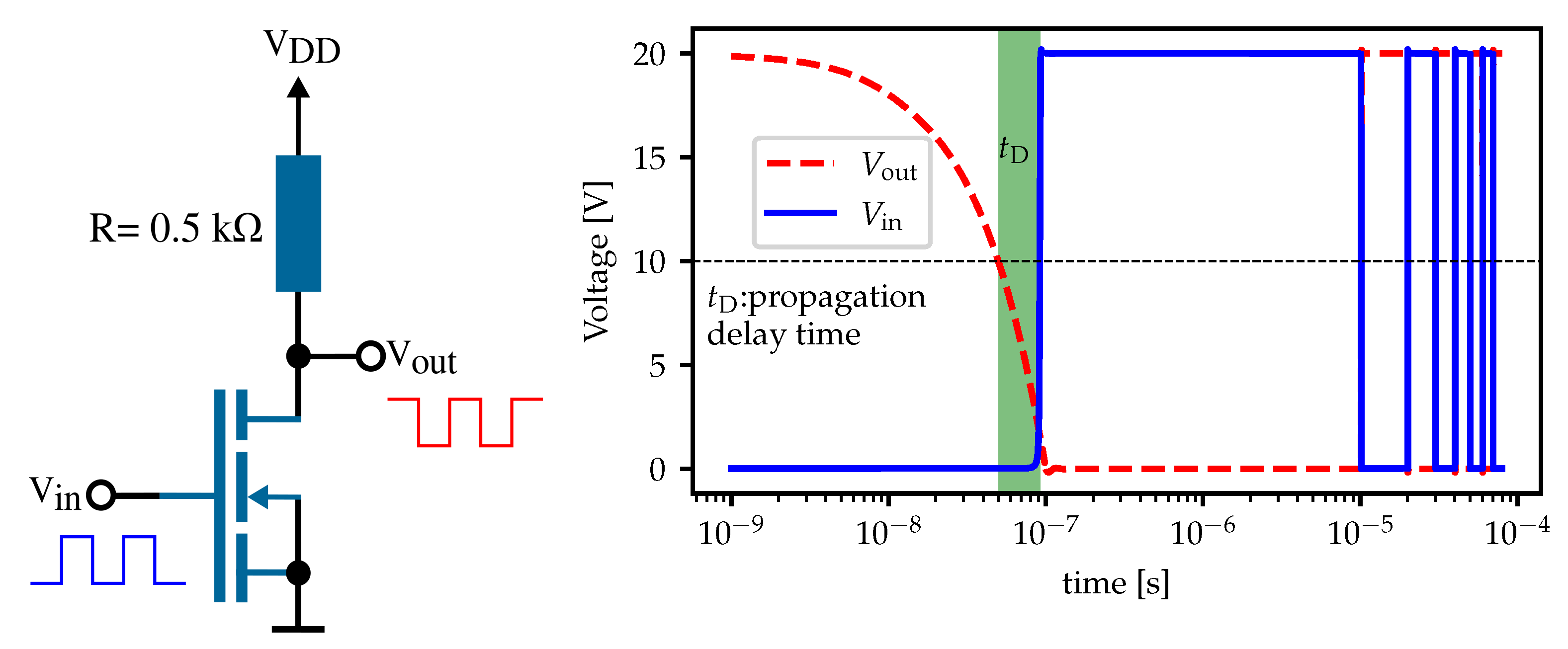
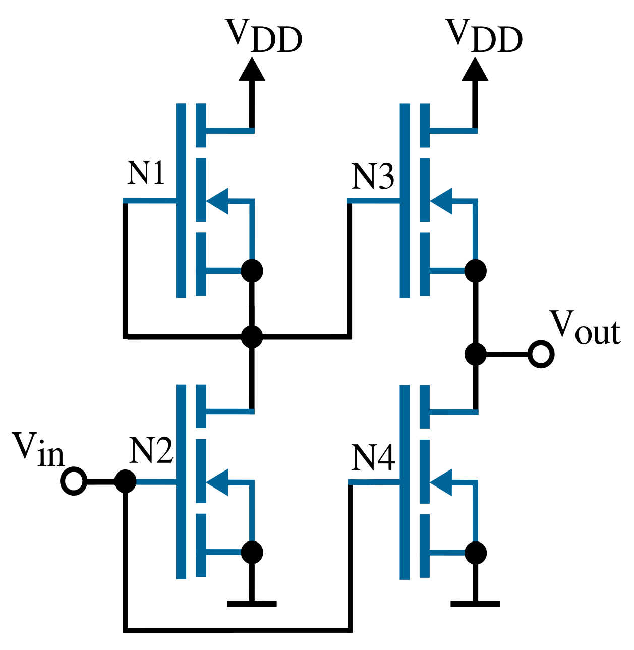
3. Compact Modeling of BTI for Circuit Simulations

As has been previously discussed, with the compact models provided for circuit simulations, the static device behavior can be nicely reproduced. However, such models do not account for time-dependent changes in the device characteristics. To consider the impact of BTI on the transistors using spice simulations, we have to extend the model by adding an independent voltage source to the gate of the transistors. This additional voltage source accounts for the threshold voltage drift, V th [23], and the schematic of the modified model is depicted in Figure 7.
Since the transistors are typically used in switching applications, transient circuit simulations are carried out next. For this purpose, we perform AC simulations employing ngspice and combine them with calculations made using our reliability tool for accounting the V th . The additional voltage source connected to the gate of the transistor contains the variability/degradation effects predicted employing the physical defect trapping model [24] implemented in the reliability simulator Comphy [21].
With each simulation, considering the accurate V th values, it is possible to demonstrate that an overestimation of the V th extracted values using power-law-like functions. Likewise, this difference in the V th can lead to a very pessimistic prediction of inverter circuits parameters such as the propagation delay time t D .
In Figure 8, the simulation process flow using the open-source ngspice simulator is illustrated. To perform our reliability simulations, we define the net-list of the circuit based on the spice models of the respective SiC power MOSFETs (step 1). Next, an external file contains the V th values extracted from Comphy (step 2) for a long operation time (ten years). This file is used to modify the initial net-list of the circuit. Then we extract the aged parameters of the circuit for a specific degradation and time point, taking into account the principle shown in Figure 7 (step 3). Note that such simulations can become easily computationally demanding. The simulation time depends on the number of V th values in the external file. The ngspice simulator launches a new simulation every time that the initial net-list is modified. However, this net-list modification does not significantly increase the simulation time. As a result of the circuit simulations, we obtain the aged circuit parameters at extended operation time considering the impact of BTI on the SiC MOSFETs. We can process these results to analyze the plots of the aged electrical characteristics of the device (step 4).

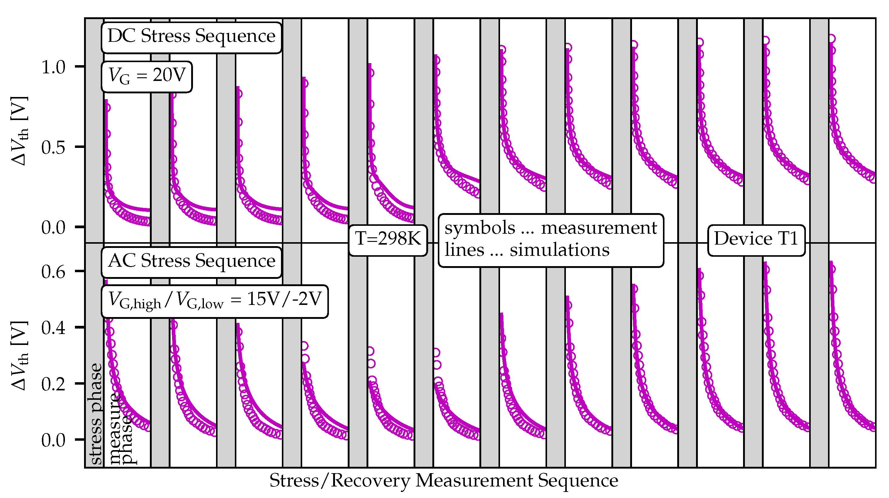
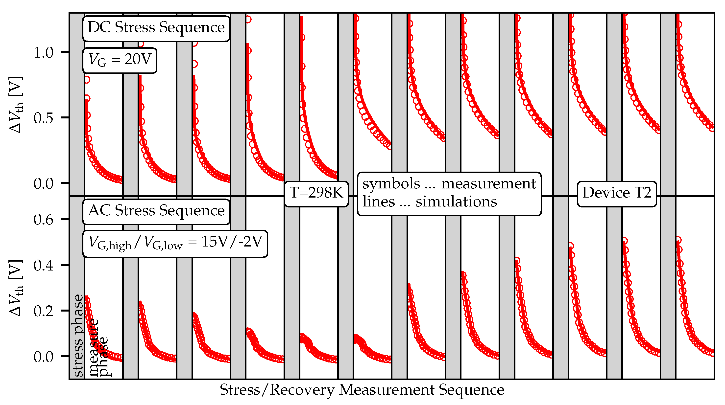
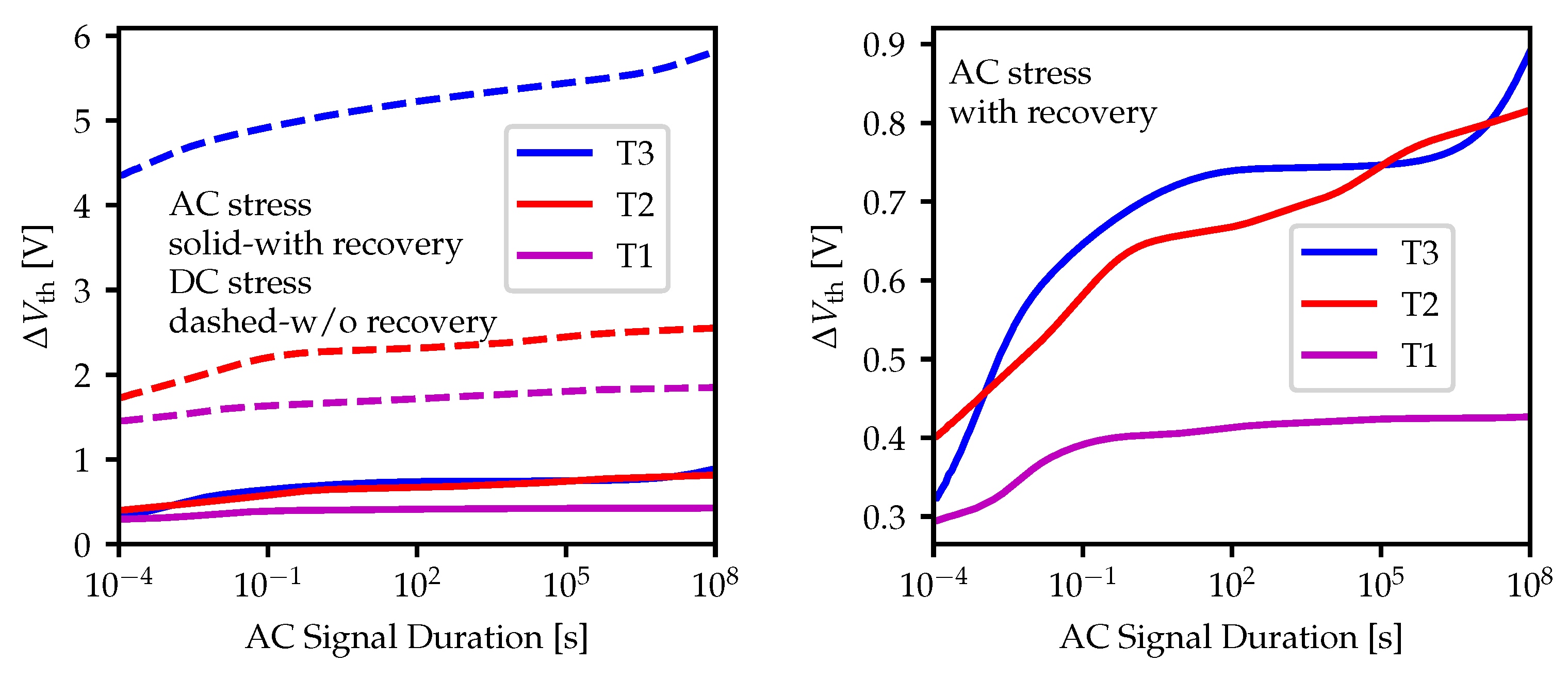
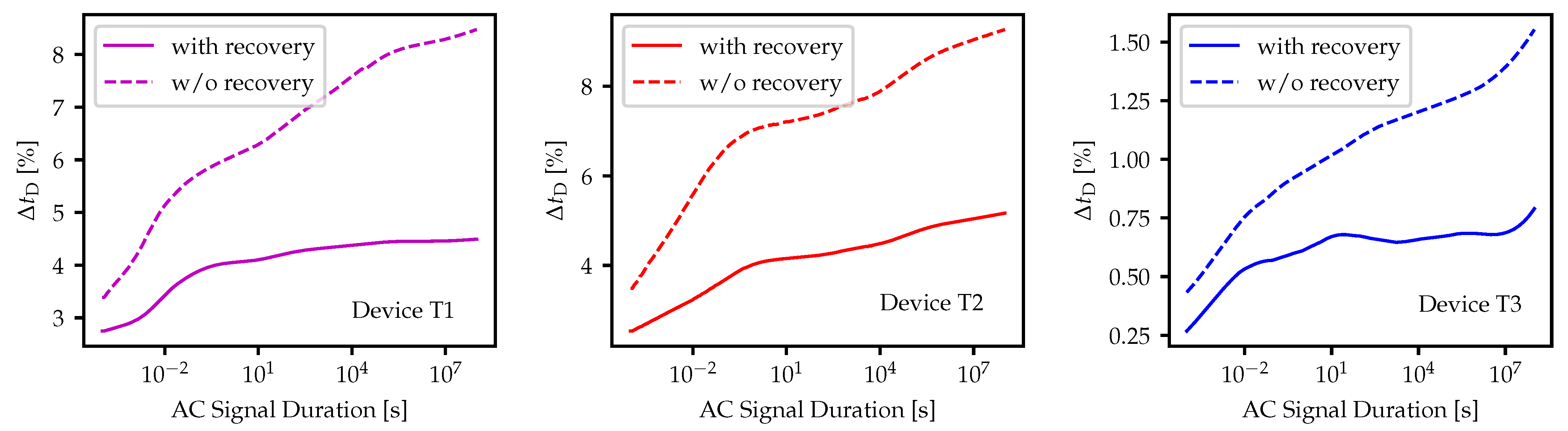
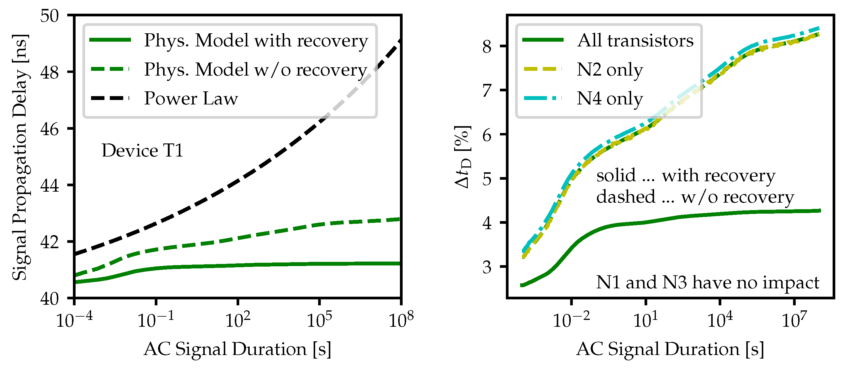
4. Results and Discussion

The first circuit we evaluate is the typical resistivity load inverter, see Figure 9 (left). With this circuit, we can efficiently verify our approach and implementation to determine the BTI impact in the propagation delay t D considering only one transistor. The values are extracted as the time difference when V in and V out are equal to V DD /2, as we show in Figure 9 (right). Each value of the delay time distribution t D represents the aging of the inverter circuit for each V th or, equivalently, for a certain degradation of the device with time.
In Figure 10 shows the V th values extracted after ten years ( 10 8 s) of operational time considering an AC input signal with a typical switching frequency for SiC applications equal to f SW = 50 kHz, duty cycle of 50%, V High = 20   V and V Low = 0   V . The time of the zero voltage in the input signal ensures the recovery phase for the V th extraction. Likewise, we consider the case for V High = V Low = 20 V (DC stress) to compare the V th values extracted when the recovery phase is omitted. For all devices the V th values are presented in the same plot for a long-term DC and short-term AC stress sequences to highlight the differences obtained between Comphy simulations with and without recovery. As can be seen, the latter leads to a significant overestimation of the V th .
As can be seen, the threshold voltage of the transistors drifts around 0.3–0.9 V after ten years of operation if the recovery phase is considered. Almost five times more, between 1.5–6 V, if the recovery phase is omitted. The propagation delay time for the resistivity load inverter circuit based on the different commercial SiC transistors T1, T2, and T3, considering the V th extracted values, are presented in Figure 11. These results represent the BTI impact on the simple test inverter circuit considering only the degradation of one transistor independently for a long operating time. Considering V th = 0 (fresh simulations), the extracted propagation delay time for the three technologies was 39 ns, 78 ns, and 169 ns for T1, T2, and T3, respectively. An increase of the threshold voltage drift over time also causes an increase in the propagation delay time of the inverter circuit. In all the cases, the increase of the propagation delay time t D is expressed in (%) and represents the difference between the t D for a specific operating time ( V th 0 ) and the initial value ( V th = 0). After ten years of operating time t D increases up to 41 ns, 85 ns, and 172 ns, for T1, T2, and T3, respectively. From these results, we can note that the increase of the propagation delay time is similar (between 2–4 ns) for each technology. However, the BTI impact (computed as an increase of the propagation delay time, see Figure 11) on T1/T2 technologies (8%) is more significant than for T3 (1.5%). One possible explanation for this is due the propagation delay time is one order higher for T3 technology. Finally, our results also show that when the recovery phase is omitted, the t D is overestimated for all technologies.
The following circuit we analyze is the pseudo-D CMOS inverter. In literature, this circuit is proposed for thin-film transistors [25,26] to implement inverters employing mono-type transistors. We make use of our simulation approach and extract the t D for a pseudo-D CMOS inverter circuit, shown in Figure 12, designed with mono-type transistors [27]. For the analysis of this circuit, it is essential to mention that we only use the T1 device. Considering that these devices were fabricated for only one channel width and length, it was impossible to design this inverter with T2 and T3 due to impedance coupling. However, thanks to the Kelvin Source pin architecture (which allows more voltage applied between the gate and source, resulting in a faster dynamic switching and reduction of the inductive effects at the gate of the device), it was possible to design and simulate the pseudo-D CMOS inverter circuit using the T1 device.
For this circuit, we compute the total degradation by evaluating V th of each transistor individually at each simulation time step. Figure 13 shows the t D distribution values for ten years of operation considering the degradation of all transistors at the same time and the degradation of each transistor individually. An overestimation of the propagation delay of the pseudo-D logic inverter circuit for a long operation time can be observed. The propagation delay t D is a few nanoseconds larger when the recovery phase of the AC signal is omitted for each transistor. This can lead to challenges for circuits operating at higher frequencies. Note that this difference in the predicted delay does not arise from real devices, but rather is a consequence of the inaccuracy of simple models. The results for N2 and N4 show a similar impact on t D . On the other hand, for N1 and N3, the circuit seems to be practically insensitive to BTI.

5. Conclusions

For a highly accurate description of the behavior of aging circuits, physical device models are required for circuit simulations. However, existing approaches use compact models that are typically based on simple mathematical formulas for circuit analysis and cannot account for aging mechanisms such as BTI at a very high accuracy over a wide range of temperature, bias and operating conditions. In our work, we combine our transistor reliability simulator Comphy with circuit simulations made using ngspice. We employ three transistor technologies and extend the compact models provided by the device vendors to be suitable for precise BTI evaluation. After Comphy is calibrated to extensive DC and AC measurements, we evaluate the propagation delay of the inverter circuits. Specifically, we analyze the resistivity load inverter circuit and the pseudo-D-CMOS inverter based on the same three different technologies, T1, T2, and T3. Our results show that the BTI has a more significant impact on T1/T2 technology than T3. On the other hand, the same results demonstrate that employing simple power-law-like formulas leads to an overestimation of the signal propagation delay, leading to severe challenges during circuit design. We also demonstrate that omitting device recovery during the low-phase under AC operation leads to a considerable overestimation of the signal propagation delay of the circuits.

Author Contributions

Conceptualization, Y.H. and M.W.; methodology, Y.H., B.S., T.G. and M.W.; investigation, Y.H.; writing—review and editing, Y.H., B.S., T.G. and M.W.; supervision, T.G. and M.W. All authors have read and agreed to the published version of the manuscript.

Funding

The financial support by the Austrian Federal Ministry for Digital and Economic Affairs, the National Foundation for Research, Technology and Development and the Christian Doppler Research Association is gratefully acknowledged. Furthermore, The research leading to these results has received funding from the from the Take-off program of the Austrian Research Promotion Agency FFG (projects no. 867414, and 861022).

Acknowledgments

Stimulating discussions with and support by Katja Waschneck and Hans Reisinger, both Infineon Munich, are gratefully acknowledged. The authors acknowledge TU Wien Bibliothek for financial support through its Open Access Funding Programme.

Conflicts of Interest

The authors declare no conflict of interest.

References

  1. Pulvirenti, M.; Montoro, G.; Nania, M.; Scollo, R.; Scelba, G.; Cacciato, M.; Scarcella, G.; Salvo, L. 2018 IEEE Energy Conversion Congress and Exposition (ECCE); IEEE: Portland, OR, USA, 2018; pp. 1895–1902. [Google Scholar]
  2. Dimitrijev, S. SiC Power MOSFETs: The current status and the potential for future development. In Proceedings of the 30th International Conference on Microelectronics (MIEL 2017), Nis, Serbia, 9–11 October 2017. [Google Scholar] [CrossRef] [Green Version]
  3. Litchtenwalner, D.J.; Hull, B.; Van Brunt, E.; Sabri, S.; Gajewski, D.A.; Grider, D.; Allen, S.; Palmour, J.W. Reliability studies of SiC vertical power MOSFETs. In Proceedings of the 2018 IEEE International Reliability Physics Symposium (IRPS), Burlingame, CA, USA, 11–15 March 2018. [Google Scholar] [CrossRef]
  4. Berens, J.; Weger, M.; Pobegen, G.; Aichinger, T.; Rescher, G.; Schleich, C.; Grasser, T. Similarities and Differences of BTI in SiC and Si Power MOSFETs. In Proceedings of the IRPS, Dallas, TX, USA, 28 April–30 May 2020. [Google Scholar] [CrossRef]
  5. Barbagallo, C.; Rizzo, S.; Scelba, G.; Scarcella, G.; Cacciato, M. On the Lifetime estimation of SiC power MOSFEts for motor drive applications. Electronics 2021, 10, 324. [Google Scholar] [CrossRef]
  6. Guevara, E.; Herrera-Perez, V.; Rocha, C.; Guerrero, K. Threshold Voltage Degradation for n-Channel 4H-SiC power MOSFETs. J. Low Power Electron. Appl. 2020, 10, 3. [Google Scholar] [CrossRef] [Green Version]
  7. www.wolfspeed.com. Available online: https://www.wolfspeed.com/document-library/?documentType=ltspice-and-plecs-models&productLine=power (accessed on 10 July 2021).
  8. www.st.com. Available online: https://www.st.com/en/power-transistors/wide-bandgap-transistors.html#cad-resource (accessed on 10 July 2021).
  9. Waltl, M.; Rzepa, G.; Grill, A.; Wolfgang, G.; Franco, J.; Kaczer, B.; Witters, L.; Mitard, J.; Horiguchi, N.; Grasser, T. Superior NBTI in High-k Si-Ge Transistors—Part I: Experimental. IEEE Trans. Electron Devices 2017, 64, 2092–2098. [Google Scholar] [CrossRef]
  10. Habersat, D.B.; Lelis, A.J.; Green, R. Measurement considerations for evaluating BTI effects in SiC MOSFETs. Microelectron. Reliab. 2018, 81, 121–126. [Google Scholar] [CrossRef]
  11. Green, R.; Lelis, A.; Habersat, D. Threshold-voltage bias- temperature instability in commercially-available SiC MOSFETs. Jpn. J. Appl. Phys. 2016, 55. [Google Scholar] [CrossRef]
  12. Peters, D. Investigation of threshold voltage stability of SiC MOSFETs. In Proceedings of the 2018 IEEE 30th International Symposium on Power Semiconductor Devices and ICs (ISPSD), Chicago, IL, USA, 13–17 May 2018; pp. 42–43. [Google Scholar] [CrossRef]
  13. Toledano-Luque, M.; Kaczer, B.; Simoen, E.; Roussel, P.; Veloso, A.; Grasser, T.; Groeseneken, G. Temperature and Voltage Dependences of the Capture and Emission Times of Individual Traps in High-k Dielectrics. Microelectron. Eng. 2011, 88, 1243–1246. [Google Scholar] [CrossRef]
  14. Kim, J.J.; Linder, B.P.; Rao, R.M.; Kim, T.H.; Lu, P.F.; Jenkins, K.A.; Kim, C.H.; Bansal, A.; Mukhopadhyay, S.; Chuang, C.T. Reliability monitoring ring oscillator structures for isolated/-combined NBTI and PBTI measurement in high-k metal gate technologies. In Proceedings of the 2011 International Reliability Physics Symposium, Monterey, CA, USA, 10–14 April 2011. [Google Scholar] [CrossRef]
  15. Miki, H.; Tega, N.; Yamaoka, M.; Frank, D.J.; Bansal, A.; Kobayashi, M.; Cheng, K.; D’Emic, C.P.; Ren, Z.; Wu, S.; et al. Statistical measurement of random telegraph noise and its impact in scaled-down high-k/metal-gate MOSFETs. In Proceedings of the 2012 International Electron Devices Meeting, San Francisco, CA, USA, 10–13 December 2012. [Google Scholar] [CrossRef]
  16. Rzepa, G.; Franco, J.; Subirats, A.; Jech, M.; Chasin, A.; Grill, A.; Waltl, M.; Knobloch, T.; Stampfer, B.; Chiarella, T.; et al. Efficient Physical Defect Model Applied to PBTI in High-k Stacks. In Proceedings of the 2017 IEEE International Reliability Physics Symposium (IRPS), Monterey, CA, USA, 2–6 April 2017. [Google Scholar] [CrossRef]
  17. Schleich, C.; Waldhoer, D.; Waschneck, K.; Feil, M.W.; Reisinger, H.; Grasser, T.; Waltl, M. Physical Modeling of Charge Trapping in 4H-SiC DMOSFET Technologies. IEEE Trans. Electron Devices 2021, 68, 4016–4021. [Google Scholar] [CrossRef]
  18. Lelis, A.J.; Habersat, D.; Green, R.; Ogunniyi, A.; Gurfinkel, M.; Suehle, J.; Goldsman, N. Time Dependence of Bias-Stress-induced SiC MOSFET Threshold-Voltage Instability Measurements. IEEE Trans. Electron Devices 2008, 55, 1835–1840. [Google Scholar] [CrossRef]
  19. Schleich, C.; Berens, J.; Rzepa, G.; Pobegen, G.; Tyaginov, S.; Grasser, T.; Waltl, M. Physical Modeling of Bias Temperature Instabilities in SiC MOSFETs. In Proceedings of the 2019 IEEE International Electron Devices Meeting (IEDM), San Francisco, CA, USA, 7–11 December 2019. [Google Scholar] [CrossRef]
  20. Grasser, T. Stochastic Charge Trapping in Oxides: From Random Telegraph Noise to Bias Temperature Instabilities. Microelectron. Reliab. 2012, 52, 39–70. [Google Scholar] [CrossRef]
  21. Rzepa, G.; Franco, J.; O’Sullivan, B.; Subirats, A.; Simicic, M.; Hellings, G.; Weckx, P.; Jech, M.; Knobloch, T.; Waltl, M.; et al. Comphy—A compact-physics framework for unified modeling of BTI. Microelectron. Reliab. 2018, 85, 49–65. [Google Scholar] [CrossRef]
  22. Puschkarsky, K.; Grasser, T.; Aichinger, T.; Gustin, W.; Reisinger, H. Review on SiC MOSFETs High-Voltage Device Reliability Focusing on Threshold Voltage Instability. IEEE Trans. Electron Devices 2019, 66, 4604–4616. [Google Scholar] [CrossRef]
  23. Martin-Martinez, J.; Ayala, N.; Rodriguez, R.; Nafria, M.; Aymerich, X. RELAB: A tool to include MOSFETs BTI and variability in SPICE simulators. In Proceedings of the 2012 International Conference on Synthesis, Modeling, Analysis and Simulation Methods and Applications to Circuit Design (SMACD), Seville, Spain, 19–21 September 2012. [Google Scholar] [CrossRef]
  24. Grasser, T.; Kaczer, B.; Goes, W.; Reisinger, H.; Aichinger, T.; Hehenberger, P.; Wagner, P.J.; Schanovsky, F.; Franco, J.; Roussel, P.; et al. Recent Advances in Understanding the Bias Temperature Instability. In Proceedings of the 2010 International Electron Devices Meeting, San Francisco, CA, USA, 6–8 December 2010. [Google Scholar] [CrossRef]
  25. Fukuda, K.; Sekitani, T.; Yokota, T.; Kuribara, K.; Huang, T.C.; Sakurai, T.; Zschieschang, U.; Klauk, H.; Ikeda, M.; Kuwabara, H.; et al. Organic Pseudo-CMOS Circuits for Low-Voltage Large-Gain High-Speed Operation. IEEE Electron Device Lett. 2011, 32, 1448–1450. [Google Scholar] [CrossRef]
  26. Huang, T.C.; Fukuda, K.; Lo, C.M.; Yeh, Y.H.; Sekitani, T.; Someya, T.; Cheng, K.T. Pseudo-CMOS: A Design Style for Low-Cost and Robust Flexible Electronics. IEEE Trans. Electron Devices 2011, 58, 141–150. [Google Scholar] [CrossRef]
  27. Kuroki, S.; Kurose, T.; Nagatsuma, H.; Ishikawa, S.; Maeda, T.; Sezaki, H.; Kikkawa, T.; Makino, T.; Ohshima, T.; Östling, M.; et al. 4H-SiC Pseudo-CMOS Logic Inverters for Harsh Environment Electronics. Mater. Sci. Forum 2017, 897, 669–672. [Google Scholar] [CrossRef]
Figure 1. Schematic of the potential energy surfaces of our physical defect model and the corresponding model parameters required to calculate the charge trapping at defects. The model is based on non-radiative multi-phonon (NMP) theory to calculate the transition times at single defects corresponding to charge transfer reactions.
Crystals 11 01150 g001
Figure 2. The prediction of the two-state model is shown versus power-law like functions for the three technologies evaluated in this work: T1 (top-left), T2 (top-right) and T3 (bottom). As can be seen, our simulations nicely replicate the experimental data, while the power-law (black) significantly deviates from the experimental data. The measurement delay for recording V G after stress for this setup is t read = 1 μs.
Crystals 11 01150 g002
Figure 3. Schematic of the MSM measurement sequences of the input signals that are applied to the gate terminal of the transistors. The V th values are extracted considering, (left) a long-term DC PBTI degradation where a constant stress bias is applied before the recovery phase is recorded, and (right) a short-term AC V th is measured at different time points ( t AC , interrupt ) at which the short AC stress is interrupted [22].
Crystals 11 01150 g003
Figure 4. Comparison between simulation and experimentally V th extracted values for T1. The simulations nicely reproduce the measured data set V th .
Crystals 11 01150 g004
Figure 5. Similar measurement sequence as shown in Figure 4 is presented here for T2. Again our model agrees well with the experimental data.
Crystals 11 01150 g005
Figure 6. Also the data recorded employing T3 can be reconstructed at high accuracy by our physical computer models.
Crystals 11 01150 g006
Figure 7. The BTI impact on the transistors is represented by adding a voltage source with a value equal to V th to the gate of the devices implemented in the Spice simulator. V th values are extracted from the accurate physical defect trapping model.
Crystals 11 01150 g007
Figure 8. Simulation process flow using open-source simulator ngspice, to analyze the BTI impact on the inverter circuits performance. The spice simulator uses the data from the reliability simulator Comphy to modify the initial net-list of the circuit. It launches simulations to extract the aged circuit parameters for long operation time. Each simulation (step 3) corresponds to an inevitable degradation of the transistors for a specific time (step 2).
Crystals 11 01150 g008
Figure 9. Schematic of the resistivity load inverter used as simple test circuit with R = 0.5   k Ω , V DD = 20   V (left) and propagation delay time t D extraction at T = 298 K (right). The latter is defined as the time difference when the output V out and input voltage V in equals V DD /2.
Crystals 11 01150 g009
Figure 10. Threshold voltage drift ( V th ) behavior extracted employing Comphy for the different SiC power MOSFETs used in this work, i.e., T1, T2 and T3 at room temperature (T = 298 K), for an AC input signal with duty cycle = 0.5 , f = 50 kHz and a stress time equal to t str = 100 ms. A comparison of the extracted values when the recovery phase is considered and omitted is shown (left). A more detailed representation of the short-term AC stress case is depicted (right).
Crystals 11 01150 g010
Figure 11. The impact of BTI on the propagation delay time for the resistivity load inverter circuit based on T1 (left), T2 (center), and T3 devices (right) is shown. For the three technologies, after ten years of the operating time, t D is overestimated around by 2–4 ns if the recovery phase in the AC input signal is omitted. The results show a BTI impact less significant on T3 than in the other ones.
Crystals 11 01150 g011
Figure 12. Schematic representation of the pseudo-D CMOS inverter circuit using commercially available SiC power MOSFETs. We analyze the BTI impact on the circuit performance considering the degradation of the V th of the transistors.
Crystals 11 01150 g012
Figure 13. Extracted signal propagation delay for the pseudo-CMOS inverter circuit considering the impact of BTI for ten years of operating time. A comparison of the results when simple power-law-like functions and physical models are used is shown (left). While N1 and N3 have no to impact on t D , the propagation delay is affected by N2 and N4 in a similar way (right).
Crystals 11 01150 g013
Publisher’s Note: MDPI stays neutral with regard to jurisdictional claims in published maps and institutional affiliations.

