
Stepwise Current Increment Sintering of Silver Nanoparticle Structures
by
 , , and
Dongkeun Kim
1, 
Arif Hussain
1,
Hee-Lak Lee
1,
Yoon-Jae Moon
1,2,
Junyoung Hwang
2 and
Seung-Jae Moon
1,* 1
Department of Mechanical Convergence Engineering, Hanyang University, Seoul 04763, Korea
2
Korea Institute of Industrial Technology, Ansan 15588, Korea
*
Author to whom correspondence should be addressed.
Crystals 2021, 11(10), 1264; https://0-doi-org.brum.beds.ac.uk/10.3390/cryst11101264
Submission received: 25 September 2021
/
Revised: 10 October 2021
/
Accepted: 14 October 2021
/
Published: 18 October 2021
Abstract
:Owing to its unique properties, silver (Ag) in the form of nanoparticle (NP) ink promises to play a vital role in the development of printed and flexible electronics. Once printed, metal NP inks require a thermal treatment process called sintering to render them conductive. Among the various methods, electrical sintering is a highly selective and rapid sintering method. Here, we studied the electrical sintering of inkjet-printed Ag NP lines via a stepwise current increment sintering (SCIS) technique. In the SCIS technique, the supplied electric current was gradually increased in multiple steps from low electric currents to higher electric currents to avoid thermal damage to the printed Ag NP ink lines. In less than 0.15 s, a line resistivity as low as 6.8 μΩcm was obtained which was comparable with furnace sintered line resistivity of 6.13 μΩcm obtained at 250 °C in 600 s. Furthermore, a numerical model was developed for the SCIS process temperature estimation. The results enabled us to elaborate on the relationship between the Ag NP line resistivity and the process temperature under various electric currents. Under the applied SCIS technique, a stable sintering process was carried out avoiding the conductive ink line and substrate damage.
1. Introduction
The progress in the patterning of electronic devices via photolithography led us to the world of the 4th industrial revolution. This lithographic technique was a revolutionary invention by Joseph Nicéphore Niépce in 1820, which led to the fabrication of the first transistor in 1947 [1]. Since then, photolithography has been playing a vital role in the advancement of the electronic industry. However, it is a complex, expensive, and slow process and not suitable for large-scale fabrication. Moreover, the high amount of hazardous chemicals used in the process [2] makes photolithography extremely dangerous both for the industrial employees and the outside environment. During the process, the photoresist materials are applied that enable the formation of the desired electronic patterns. However, these materials are hazardous chemicals that cause fatal diseases [3,4,5,6] for industry employees. In addition, the edge beam removal of the undesired photoresist by heating and the chemical change in the photoresist by the ultraviolet light produces additional by-products [2,7]. The disposal of such waste is an environmentally dangerous chemical process [3,8]. On the other hand, conductive inks used for direct metal printing and sintering are much safer. The triethylene glycol monomethyl ether (TGME) is used as a binder in the nanoparticle (NP) ink which simply decomposes to water and carbon dioxide during the sintering process. Furthermore, in the direct metal printing technique, the patterning of the metal interconnects can be realized in a single step, reducing the time, cost, and waste production [9,10]. The most common metal nanoparticles used for direct metal printing in printed electronics are silver (Ag) [10], gold (Au) [11], and copper (Cu) nanoparticles [12] particularly due to their high electrical conductance.
The direct metal printing technique involves the ink materials, either in the form of metalorganic precursors [11] or metal nanoparticles suspended in dispersants (particle-based conductive inks containing organic shells). The dispersants are adopted to prevent the agglomeration of the nanoparticles in the ink. Secondly, organic binders are used to assure mechanical integrity and adhesion to the substrate by Van der Waals forces after drying [12]. However, these organic binders need to be removed in a process called sintering to render the ink conductive. Multiple sintering techniques have been reported throughout the years, such as oven sintering [12], laser sintering [13,14], microwave sintering [15], infrared sintering [16], room temperature sintering [17], intense pulsed light sintering [18], and plasma sintering [19]. As an alternative to the above methods, electrical sintering, which sinters the conductive ink line via Joule heating, is a facile choice [10,20,21]. Besides the high selectivity, electrical sintering offers an extremely rapid sintering process. Allen et al. [21] studied the constant voltage method to sinter a 5 mm × 60 ± 10 μm Ag NP line within 4 ms and obtained a very low resistivity value. During the sintering process, the majority of the resistance drop occurred within 2 μs, which indicated the extremely fast nature of the electrical sintering process.
During a single step constant voltage method, the current is not increased when a voltage is less than a certain threshold voltage. After the voltage reaches a threshold voltage, there is a sudden surge of electric current through the NP line. The sudden surge of the electric current can be detrimental to NP line and cause thermal damage, especially at high initial line resistances [22]. To overcome this problem, a two-step input voltage method was suggested by Jang et al. (2013) [22]. However, the voltage input method’s drawback is the lack of control over the current regulation once the percolation network is formed among the nanoparticles [23]. Secondly, large input voltage is required to overcome the initial line resistance [21] even in a two-step voltage supply [22]. Whereas less than 1 A of constant current is enough to effectively generate thermal energy to sinter the printed line within milliseconds. Therefore, we devised the stepwise current increment sintering (SCIS) method, which enabled the control of current regulation and hence, provided control over the process temperature and the final resistance of the conductive lines. Within 0.15 s we obtained around 6.8 μΩcm in a electrical current sintering process without thermal damage to the printed conductive lines. Conventionally, about 7 μΩcm resistivity is regarded to be sufficient for a thin conductive line [24]. The SCIS sintering method using various electric currents was demonstrated and in situ resistivity during the sintering process was measured. For the temperature analysis during the SCIS method, a numerical model was developed to estimate the sintering process temperature.
2. Materials and Methods
2.1. Experimental Setup
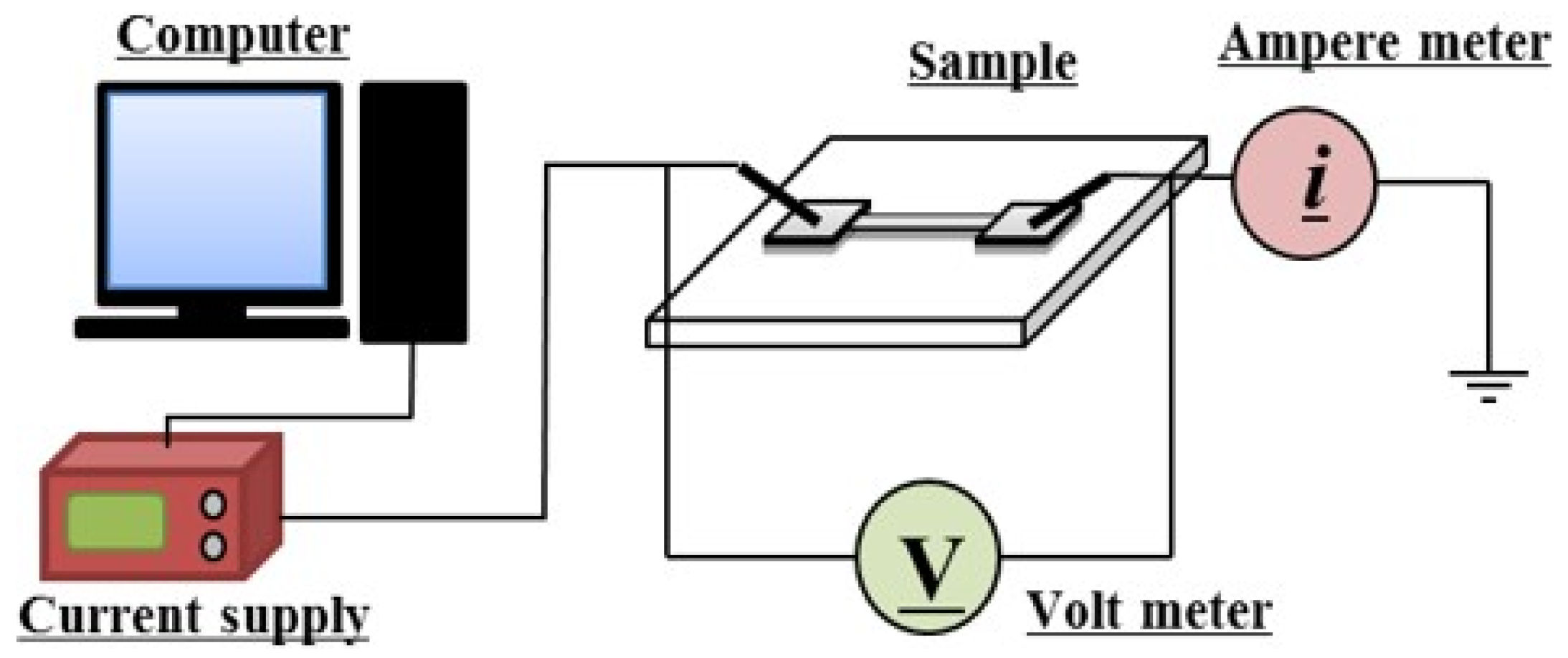
A commercial silver nanoparticle ink dispersed in TGME (Advanced Nano Products, DGP 40LT-15C) with ~34 wt% and an average size of ~50 nm was used in this study. The recommended curing temperature for the ink was 120–150 °C. The surface tension and viscosity of the ink were 35–38 mNm−1 and 10–17 mPa·s, respectively. Samples were prepared as follows: Initially, glass substrates (Samsung-Corning, Eagle XG 2000) were ultrasonically cleaned in acetone and Isopropyl Alcohol (IPA) for 10 min each. Afterward, the residual moisture was removed by hotplate heating of the substrates at 110 °C for 30 min. The ink lines were printed onto the substrates by a DMP-2831 ink-jet printer (Dimatix, Santa Clara, CA, USA). Initially, two identical pads were printed on the substrates and sintered at 250 °C for half an hour to prevent the error in measuring the electrical resistivity. Afterward, the sample lines (3000 μm × 130 μm × 0.308 μm) were printed in a manner that connected the two pads [22]. After the lines were printed, the cross-sectional information of the printed lines was measured using Alpha-Step IQ (KLA-Tencor, CA, USA.) in order to regulate the structure geometry. To minimize the high initial resistance, the samples were dried on a hotplate at 55 °C for 300 s because the high initial resistance prevents the electrical current flow through the Ag NP lines. During the electrical sintering process, the stepwise current was controlled by a power supply (Kikusui, PBZ 40–10). Figure 1 illustrates the schematic setup of the SCIS method.
2.2. Temperature Calculation
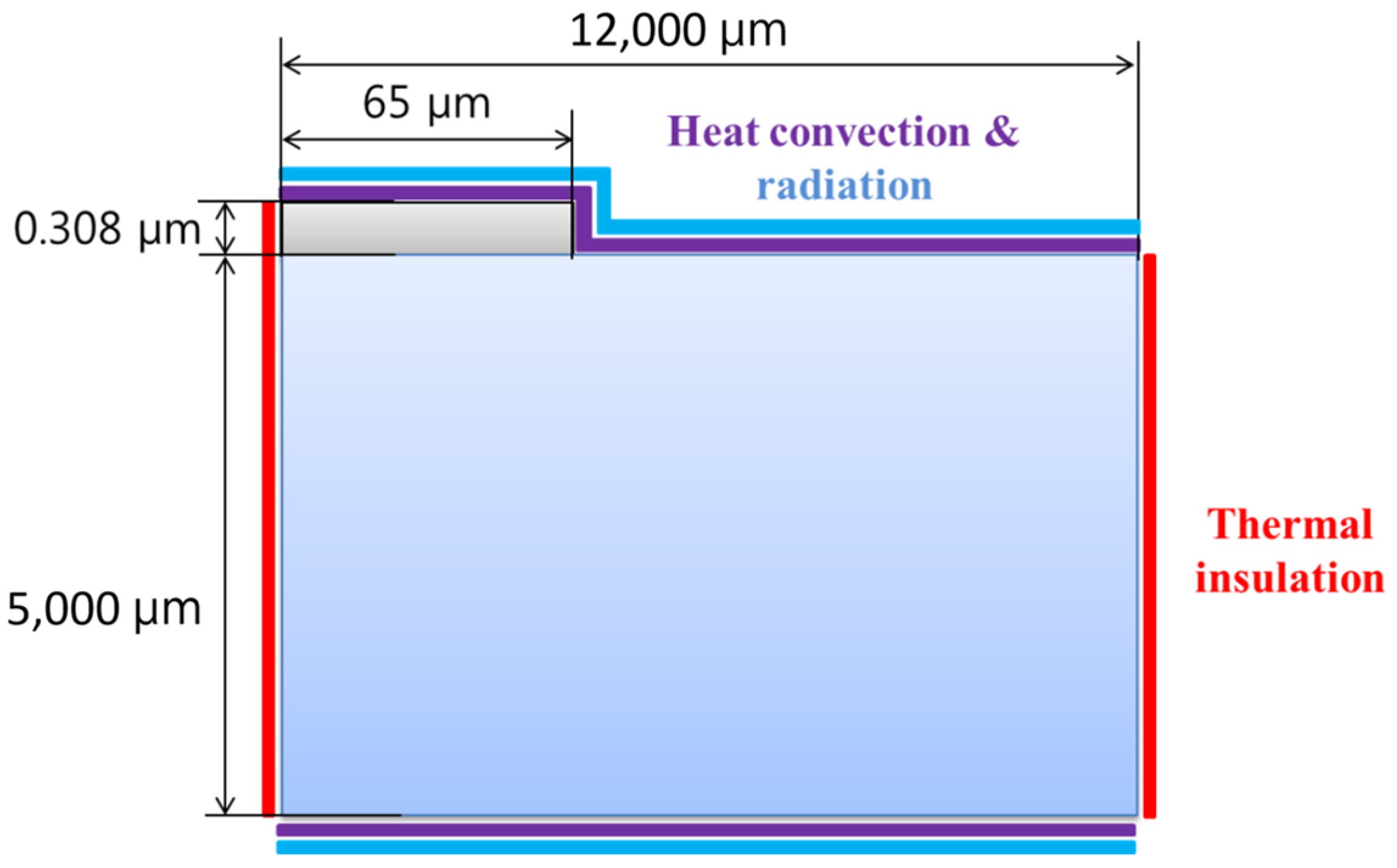
Heat is the driving force during the sintering process, which directly translates to a rise in the temperature during the process. This rise in process temperature during sintering and its control is the deciding factor behind the applicability of the sintering technique. For example, typically higher temperatures provide much better sintering results [17,25,26]. However, this restricts the use of temperature-sensitive substrates [16,27]. Therefore, the measurement of the process temperature during sintering is essential. As the electrical sintering completes within milliseconds, in situ temperature monitoring of the process is not feasible. Hence, we estimated the process temperatures via numerical modeling in COMSOL Multiphysics. This computer-aided simulation was carried out by solving a two-dimensional heat conduction equation as follows.
where , , and are the density, heat capacity, and thermal conductivity of each material, respectively. For each material the subscript states: 1 for ink, 2 for glass substrate. Si stands for the heat source term for the applied Joule heating, where , R, A1, and l1, stand for the applied current, resistance, cross-sectional area, and line length of the conductive ink. The initial condition was set at 22 °C. Furthermore, the convective and radiative heat transfer boundary conditions were applied on the top and bottom surfaces of the conductive ink line and the glass substrate, and thermal insulation was applied across the sides of the glass substrate by the symmetrical cross-section as shown in Figure 2.
Finally, continuous heat flux and temperature were adopted as the interface conditions. Table 1 displays the parameters adopted in solving the two-dimensional model of Figure 2. The thermal conductivity of the ink was determined with in situ resistance measurement to reflect the variations caused by temperature change [17].
3. Results and Discussion
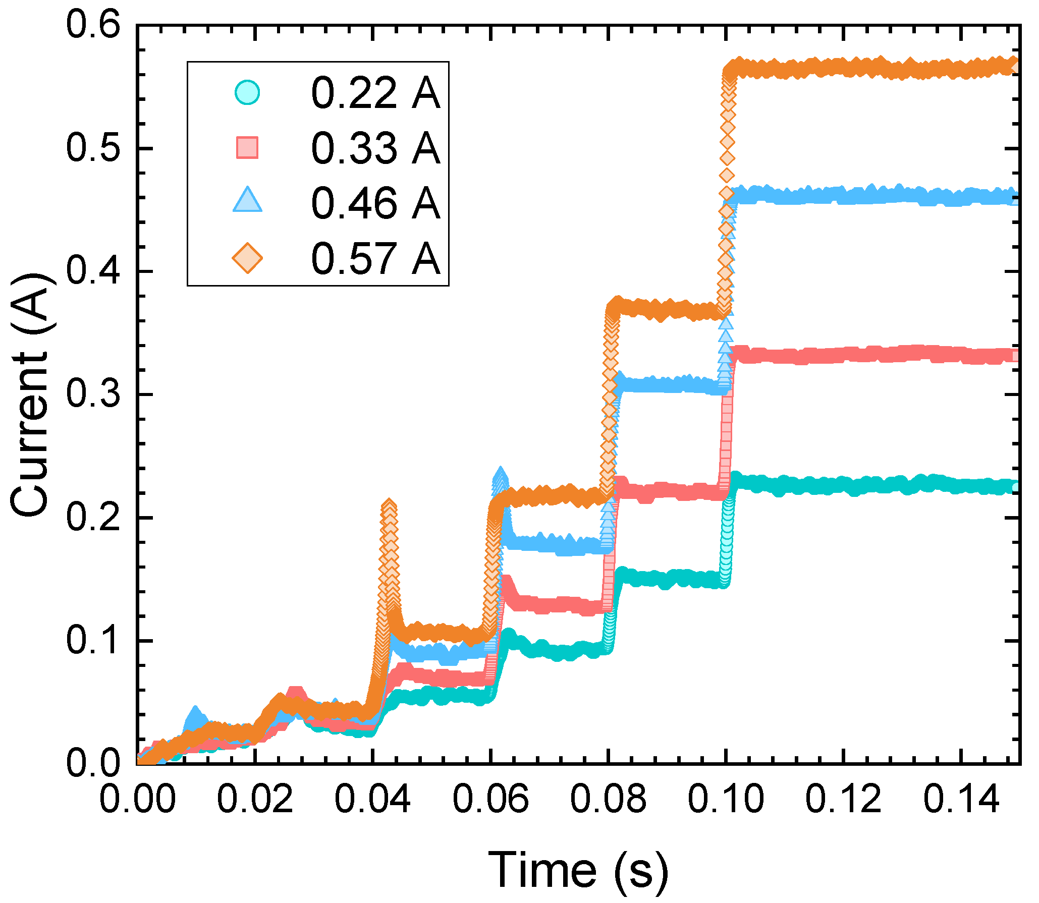
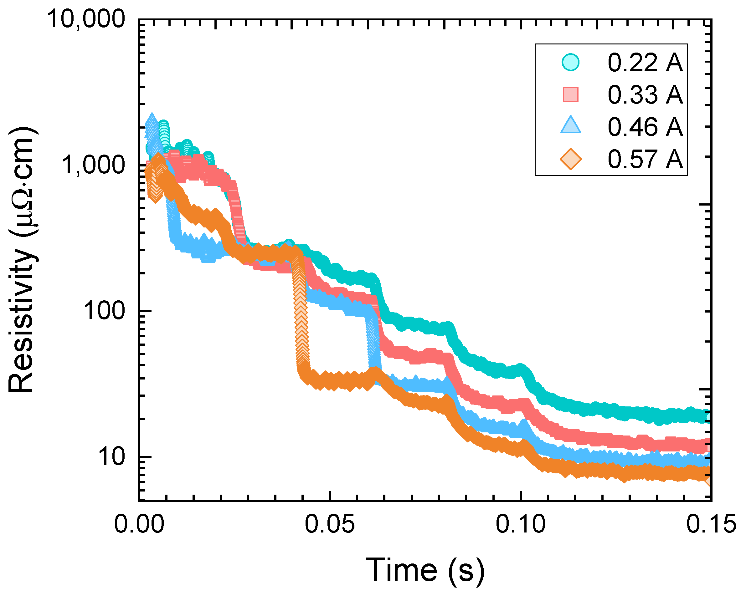
In Figure 3, the applied electric current step configurations in the SCIS method are displayed. All the configurations were composed of five steps. The currents were supplied for a total of 0.15 s. The current supply started from low currents and then increased with small steps. As the maximum temperature during the sintering process affects the final sheet resistance of the sintered lines, the final step was regulated for 0.15 s with electric currents steps of 0.22, 0.33, 0.46, and 0.57 A, respectively. For the case of 0.57 A, a surge in the electric current from 0.041 to 0.0432 s was caused due to the sudden reduction in the electrical resistance of the Ag NP line allowing the flow of a large amount of electric current. This can be confirmed from Figure 4 where at the same period we noticed a sharp reduction in the electrical resistivity. Although the constant electric current was supplied at each step, the reduction in the line resistance was too fast compared to the response time of the power supply. Therefore, during this period, the voltage drop was not compensated as a result there was a surge in the electric current, and in less than 1 ms the electric current dropped back to the supplied 0.1 A. Similar behavior for 0.33 and 0.46 A is presented in Figure 3, resulting in a sharp drop in the electrical resistivities from 0.06 to 0.064 s as shown in Figure 4.
Figure 4 displays the transient resistivity of the silver nanoparticle ink during the stepwise current increment sintering with various applied current configurations. The final resistivities of 18.6, 11.7, 8.6, and 6.8 μΩcm were obtained with the final-step currents of 0.22, 0.33, 0.46, and 0.57 A, respectively. The step current increment decreased the resistance of printed ink lines, and higher electric currents produced the lower line resistivities. The stepwise increase in the electric current indicated the stepwise increase of the electron flow per unit area of the conductive ink line. The increase in the current corresponds to the increase in the kinetic energy of the electrons. The electrons with high kinetic energy collide with the surrounding atoms inducing heat that sinters the NPs. The higher the initial NP line resistance, the larger the number of collisions of the electrons with the surrounding atoms. These collisions raise the process temperature. Consequently, high temperatures can be detrimental to the printed conductive ink line with high initial resistance causing thermal damage. Therefore, it is crucial to reduce the resistance of the NP line in a stepwise manner to avoid thermal damage.
Figure 5 depicts the estimated temperature profiles corresponding to the stepwise increment in the electric currents. The stepwise increase in the process temperature helped a smooth thermal sintering process. At different steps, we observed the trend of a decrease in the temperature followed by the attained peak temperature. This was due to the smooth flow of electrons as a result of a decrease in resistivity. However, the sharp increase in the temperature profiles for the 0.57, 0.46, and 0.33 A at different periods was caused as a result of the surge in the electric current in such periods as discussed in the previous section. The maximum estimated temperatures were 270, 342, 441, and 584 °C with the final step currents of 0.22, 0.33, 0.46, and 0.57 A, respectively. Comparing the temperature plot to the resistivity plot as shown in Figure 3, the estimated temperature profile indicated that the higher electric currents provided higher process temperatures and comparatively lower resistivity.
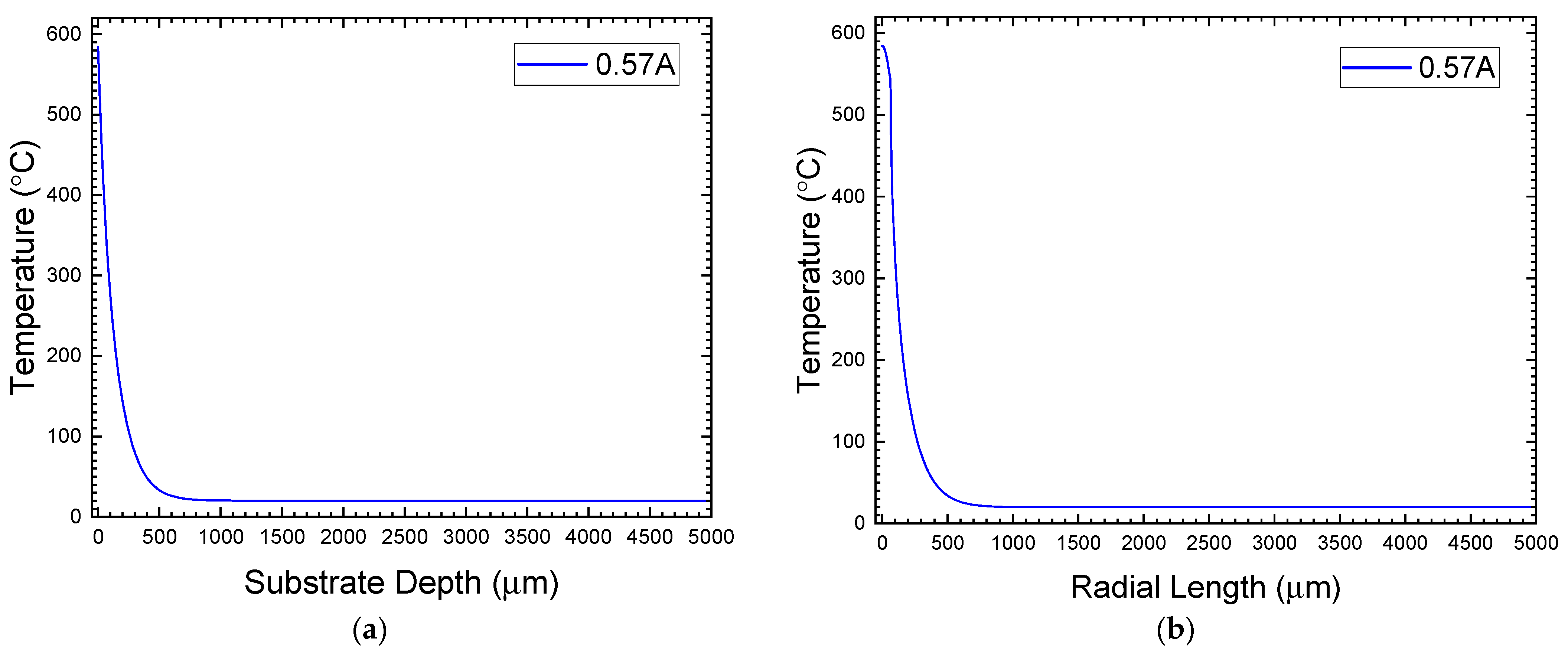
As shown in Figure 6, the temperature rise of the substrate was restricted to the direct vicinity of the silver line. This reflects the fact that one of the assets of the electrical sintering method is the preservation of the substrate damage. The magnitude of the supplied current correspondingly depicts the electrical sintering process temperature. As the current supply increased, an increase in the process temperature was observed. The increase in the process temperature drives the high energetic Ag NPs to agglomerate in an attempt to increase their surface area to accommodate for the obtained access energy. Hypothetically, if the heat generation is too fast (corresponding to a large current supply in a single step) the NPs fail to increase their surface area by joining with other NPs subsequently melting or even evaporating [28]. The stepwise supply of the electric current helps the process of NP agglomeration to develop in multiple steps i.e., from initial neck formation to a complete coalescence. Consequently, the NP line resistivity is reduced in the form of steps.
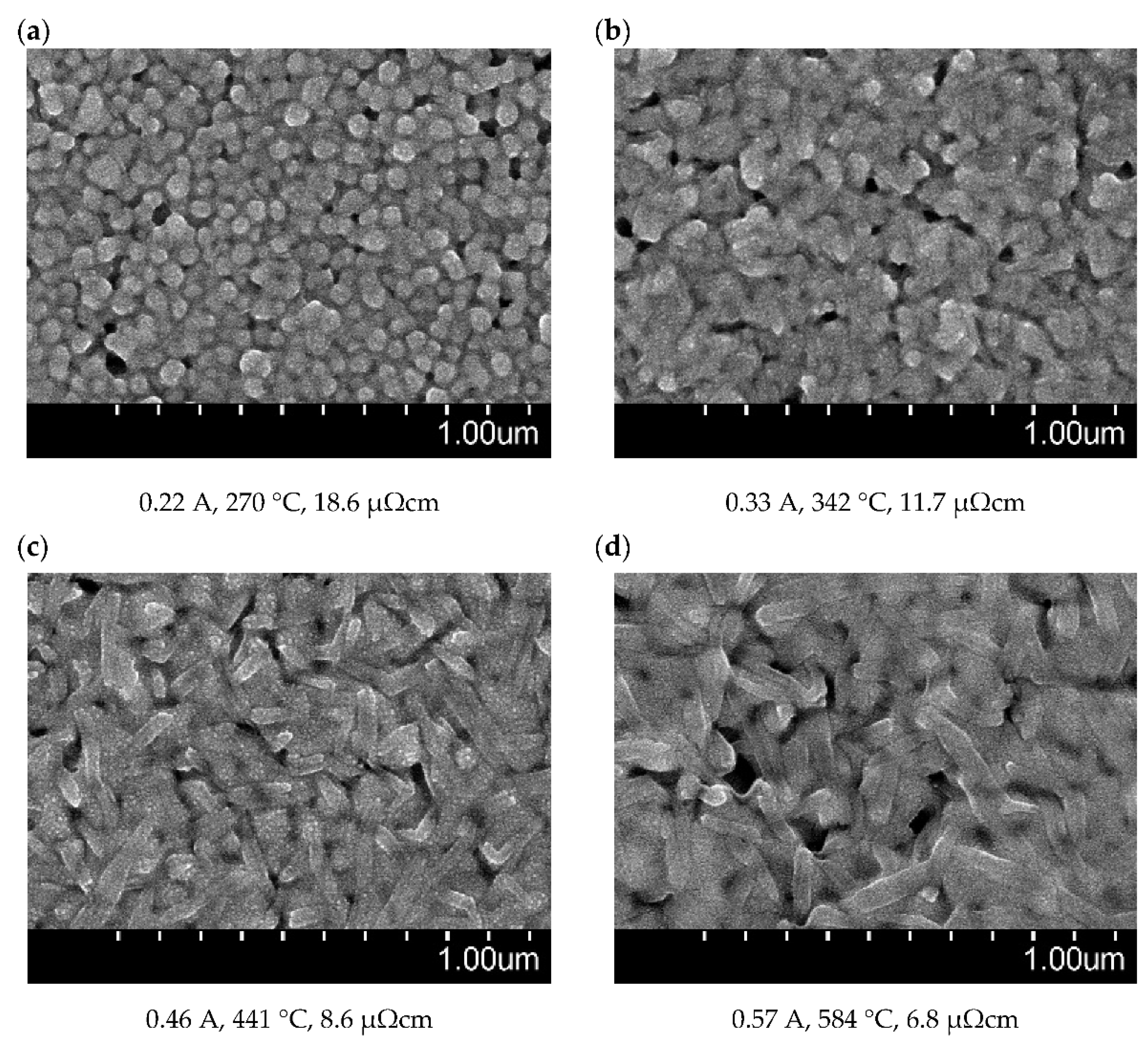
Figure 7 shows the surface morphology of the printed conductive ink line after sintered with the stepwise current increment configurations. As the final step current increased from 0.22 to 0.57 A and the maximum temperature increased from 270 to 584 °C, the resistivity dramatically decreased from 18.6 to 6.8 μΩcm. Figure 7a shows grainy surface morphology with relatively smaller grain sizes. The grainy surface morphology indicated that 0.22 A could not generate enough heat to cause a high degree of NP coalescence. Moreover, a considerable surface porosity was observed. Thus, the combined effects of the grainy structure and a porous surface resulted in the high final resistivity of 18.6 μΩcm. As the supplied current was increased to 0.33 A, the higher induced temperature (342 °C) resulted in a significantly higher degree of NP coalescence as compared to the 0.22 A case in Figure 7b. However, the surface was highly porous, which restricted the final resistivity of 11.7 μΩcm. As the current was increased to 0.46 A, the significantly higher induced temperature of 441 °C resulted in a surface structure with elongated NPs (Figure 7c), which was observed in another laser sintering study as well [26]. To find out the explanation for this elongation further work may be necessary. The NP elongation was believed to be a consequence of a high degree of NP coalescence forming long percolation networks. A minimum resistivity of 8.6 μΩcm was obtained with 0.46 A final-step current. From Figure 7a–c higher temperatures caused better NP coalescence. This resulted in NP line resistivity drop. Finally, at 0.57 A final-step current we observed the highest degree of NP coalescence as shown in Figure 7d. Longer elongated NPs were obtained in 0.57 A final-step current as compared to the 0.46 A case. Even though very large pores were observed in the SEM image, but the degree of the NP coalescence was large enough to produce a minimum resistivity of 6.8 μΩcm.
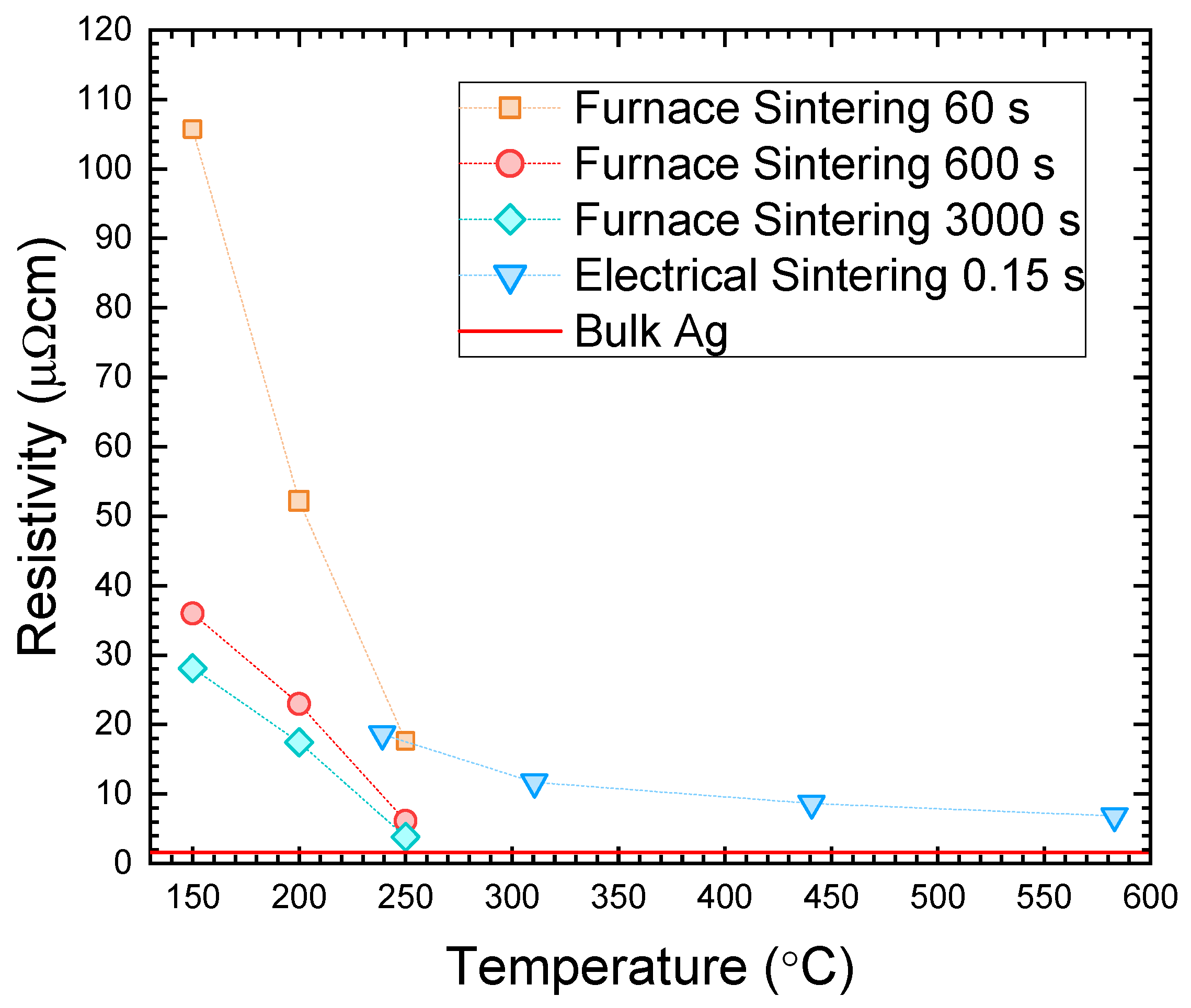
Figure 8 presents the variation of resistivities with sintering temperatures for comparing the furnace sintering and the electrical sintering via the SCIS technique. The furnace sintering times were 1, 10, and 50 min at furnace temperatures of 150, 200, and 250 °C, respectively. The maximum furnace temperature of 250 °C was selected because the best resistivity results were reported at this temperature in previous studies [27,28] without any thermal damage. The resistivity of the Ag NPs sintered in a furnace for longer durations was decreased. After the furnace sintering at 250 °C for 1, 10, and 50 minutes, the obtained Ag NP line resistivities were 17.6, 6.13, and 3.8 μΩcm, respectively. The minimum resistivity of 6.28 μΩcm was achieved in 0.15 s by the SCIS technique with 0.57 A final-step and this value was close to the Ag NP line resistivity sintered for 600 s at 250 °C via furnace sintering. The induced high temperatures with the application of the final-step current for only 0.15 s were high enough to enhance the high degree of mass diffusion for building the electron percolation network from the better neck connectivity among Ag NPs. The above observations indicated that high and locally induced Joule heating of the Ag NPs in a stepwise fashion as proposed in our study can match the performance of furnace sintering at much longer sintering durations. Nevertheless, the SCIS technique is paramount for achieving low resistivities at extremely short sintering durations and high locally induced temperatures without thermal damage to the Ag NP lines.
4. Conclusions
In this work a stepwise current increment sintering (SCIS) technique was developed during a rapid electrical sintering of inkjet-printed Ag NP lines. Line resistivity as low as 6.8 μΩcm was obtained in within as low as 0.15 s with the help of the stepwise current supply avoiding thermal damage to the sintered NP line. Comparatively, a 6.13 μΩcm line resistivity was achieved in 600 s via the conventional furnace sintering at 250 °C. In addition, the SCIS process temperatures were estimated via computer-aided simulation, which displayed a peak temperature of 584 °C for the obtained minimum resistivity case. As attaining lower resistivity values at lower temperatures are highly dependent on the size of the nanoparticles, chemical dispersants used in the inks, and the substrates, the results obtained via our SCIS method have room for improvement. Furthermore, the correspondence between the electric current and temperature can be utilized to provide smoother current variations such as a continuous ramp or parabolic signals before the final current step.
Author Contributions
Conceptualization, S.-J.M.; methodology, Y.-J.M.; software, H.-L.L.; validation, Y.-J.M. and A.H.; formal analysis, D.K.; investigation, Y.-J.M.; resources, J.H.; data curation, D.K. and A.H.; writing—original draft preparation, D.K.; writing—review and editing, S.-J.M.; supervision, S.-J.M.; project administration, S.-J.M.; funding acquisition, J.H. All authors have read and agreed to the published version of the manuscript.
Funding
This study was conducted with the support of the Korea Institute of Industrial Technology as “Development of root technology for multi-product flexible production” (KITECH EO-21-0008).
Conflicts of Interest
The authors declare no conflict of interest. The funders had no role in the design of the study; in the collection, analyses, or interpretation of data; in the writing of the manuscript, or in the decision to publish the results.
References
- Ross, I.M. The invention of the transistor. Proc. IEEE 1998, 86, 7–28. [Google Scholar] [CrossRef]
- Chelton, C.F.; Glowatz, M.; Mosovsky, J.A. Chemical Hazards in the Semiconductor Industry. IEEE Trans. Educ. 1991, 34, 269–288. [Google Scholar] [CrossRef]
- Huang, S.Z.; Wu, K.Y. Health Risk Assessment of Photoresists Used in an Optoelectronic Semiconductor Factory. Risk Anal. 2019, 39, 2625–2639. [Google Scholar] [CrossRef]
- Lee, H.E.; Kim, E.A.; Park, J.; Kang, S.K. Cancer mortality and incidence in Korean semiconductor workers. Saf. Health Work 2011, 2, 135–147. [Google Scholar] [CrossRef] [PubMed] [Green Version]
- Beall, C.; Bender, T.J.; Cheng, H.; Herrick, R.; Kahn, A.; Matthews, R.; Sathiakumar, N.; Schymura, M.; Stewart, J.; Delzell, E. Mortality among semiconductor and storage device-manufacturing workers. J. Occup. Environ. Med. 2005, 47, 996–1014. [Google Scholar] [CrossRef]
- Darnton, A.; Miller, B.G.; MacCalman, L.; Galea, K.S.; Wilkinson, S.; Cherrie, J.W.; Shafrir, A.; McElvenny, D.; Osman, J. An updated investigation of cancer incidence and mortality at a Scottish semiconductor manufacturing facility with case-control and case-only studies of selected cancers. Occup. Environ. Med. 2012, 69, 767–769. [Google Scholar] [CrossRef]
- Park, D.-U.; Byun, H.-J.; Choi, S.-J.; Jeong, J.-Y.; Yoon, C.-S.; Kim, C.-N.; Ha, K.-C.; Park, D.-Y. Review on Potential Risk Factors in Wafer Fabrication Process of Semiconductor Industry. Korean J. Occup. Environ. Med. 2011, 23, 333–342. [Google Scholar] [CrossRef]
- Kim, M.H.; Kim, H.; Paek, D. The health impacts of semiconductor production: An epidemiologic review. Int. J. Occup. Environ. Health 2014, 20, 95–114. [Google Scholar] [CrossRef] [Green Version]
- Fuller, S.B.; Wilhelm, E.J.; Jacobson, J.M. Ink-jet printed nanoparticle microelectromechanical systems. J. Microelectromech. Syst. 2002, 11, 54–60. [Google Scholar] [CrossRef] [Green Version]
- Tan, H.W.; Saengchairat, N.; Goh, G.L.; An, J.; Chua, C.K.; Tran, T. Induction Sintering of Silver Nanoparticle Inks on Polyimide Substrates. Adv. Mater. Technol. 2020, 7, 1900897. [Google Scholar] [CrossRef]
- Dearden, A.L.; Smith, P.J.; Shin, D.Y.; Reis, N.; Derby, B.; O’Brien, P. A low curing temperature silver ink for use in ink-jet printing and subsequent production of conductive tracks. Macromol. Rapid Commun. 2005, 26, 315–318. [Google Scholar] [CrossRef]
- Perelaer, J.; De Laat, A.W.M.; Hendriks, C.E.; Schubert, U.S. Inkjet-printed silver tracks: Low temperature curing and thermal stability investigation. J. Mater. Chem. 2008, 18, 3209–3215. [Google Scholar] [CrossRef]
- Bolduc, M.; Trudeau, C.; Beaupré, P.; Cloutier, S.G.; Galarneau, P. Thermal Dynamics Effects using Pulse-Shaping Laser Sintering of Printed Silver Inks. Sci. Rep. 2018, 8, 1418. [Google Scholar] [CrossRef] [Green Version]
- Lee, I.-S.; Ryu, K.; Park, K.-H.; Moon, Y.-J.; Hwang, J.-Y.; Moon, S.-J. Temperature effect on physical properties and surface morphology of printed silver ink during continuous laser scanning sintering. Int. J. Heat Mass Transf. 2017, 108, 1960–1968. [Google Scholar] [CrossRef]
- Perelaer, J.; Jani, R.; Grouchko, M.; Kamyshny, A.; Magdassi, S.; Schubert, U.S. Plasma and microwave flash sintering of a tailored silver nanoparticle ink, yielding 60% bulk conductivity on cost-effective polymer foils. Adv. Mater. 2012, 24, 3993–3998. [Google Scholar] [CrossRef]
- Tobjörk, D.; Aarnio, H.; Pulkkinen, P.; Bollström, R.; Määttänen, A.; Ihalainen, P.; Mäkelä, T.; Peltonen, J.; Toivakka, M.; Tenhu, H.; et al. IR-sintering of ink-jet printed metal-nanoparticles on paper. Thin Solid Films 2012, 520, 2949–2955. [Google Scholar] [CrossRef]
- Magdassi, S.; Grouchko, M.; Berezin, O.; Kamyshny, A. Triggering the sintering of silver nanoparticles at room temperature. ACS Nano 2010, 4, 1943–1948. [Google Scholar] [CrossRef]
- Kang, H.; Sowade, E.; Baumann, R.R. Direct intense pulsed light sintering of inkjet-printed copper oxide layers within six milliseconds. ACS Appl. Mater. Interfaces 2014, 6, 1682–1687. [Google Scholar] [CrossRef]
- Wolf, F.M.; Perelaer, J.; Stumpf, S.; Bollen, D.; Kriebel, F.; Schubert, U.S. Rapid low-pressure plasma sintering of inkjet-printed silver nanoparticles for RFID antennas. J. Mater. Res. 2013, 28, 1254–1261. [Google Scholar] [CrossRef]
- Moon, S.-J. The Effect of Temperature on the Electrical Properties of Inkjet-Printed Silver Nanoparticle Ink During Electrical Sintering. J. Nanosci. Nanotechnol. 2013, 13, 6174–6178. [Google Scholar] [CrossRef]
- Allen, M.L.; Aronniemi, M.; Mattila, T.; Alastalo, A.; Ojanperä, K.; Suhonen, M.; Seppä, H. Electrical sintering of nanoparticle structures. Nanotechnology 2008, 19, 175201. [Google Scholar] [CrossRef]
- Jang, S.; Lee, D.J.; Lee, D.; Oh, J.H. Electrical sintering characteristics of inkjet-printed conductive Ag lines on a paper substrate. Thin Solid Films 2013, 546, 157–161. [Google Scholar] [CrossRef]
- Moon, Y.J.; Lee, S.H.; Kang, H.; Kang, K.; Kim, K.Y.; Hwang, J.Y.; Cho, Y.J. Electrical sintering of inkjet-printed silver electrode for c-Si solar cells. PLoS ONE 2011, 6, e17209. [Google Scholar] [CrossRef]
- Hong, S.; Yeo, J.; Kim, G.; Kim, D.; Lee, H.; Kwon, J.; Lee, H.; Lee, P.; Ko, S.H. Nonvacuum, maskless fabrication of a flexible metal grid transparent conductor by low-temperature selective laser sintering of nanoparticle ink. ACS Nano 2013, 7, 5024–5031. [Google Scholar] [CrossRef]
- Kim, M.K.; Kang, H.; Kang, K.; Lee, S.H.; Hwang, J.Y.; Moon, Y.; Moon, S.J. Laser sintering of inkjet-printed silver nanoparticles on glass and PET substrates. In Proceedings of the 2010 10th IEEE Conference on Nanotechnology, NANO 2010, Seoul, Korea, 17–20 August 2010; pp. 520–523. [Google Scholar]
- Khan, A.; Rasmussen, N.; Marinov, V.; Swenson, O.F. Laser sintering of direct write silver nano-ink conductors for microelectronic applications. In Photon Processing in Microelectronics and Photonics VII; SPIE: San Jose, CA, USA, 2008; Volume 6879, p. 687910. [Google Scholar] [CrossRef]
- Moon, Y.J.; Kang, H.; Kang, K.; Hwang, J.Y.; Lee, J.-H.; Moon, S.-J. Effect of Laser Intensity on the Characteristic of Inkjet-Printed Silver Nanoparticles During Continuous Laser Sintering. J. Nanosci. Nanotechnol. 2014, 14, 8631–8635. [Google Scholar] [CrossRef] [PubMed]
- Halonen, E.; Viiru, T.; Östman, K.; Cabezas, A.L.; Mantysalo, M. Oven sintering process optimization for inkjet-printed Ag Nanoparticle ink. IEEE Trans. Compon. Packag. Manuf. Technol. 2013, 3, 350–356. [Google Scholar] [CrossRef]
Figure 1.
Schematic diagram of the electrical sintering setup for the SCIS technique.

Figure 2.
Schematic diagram of the two-dimensional model for the temperature estimation during the SCIS process.
Figure 2.
Schematic diagram of the two-dimensional model for the temperature estimation during the SCIS process.

Figure 3.
Stepwise electric current supply during the electrical sintering of the Ag NP lines.

Figure 4.
Transient in situ resistivities of the Ag NP lines during SCIS technique with various applied currents.
Figure 4.
Transient in situ resistivities of the Ag NP lines during SCIS technique with various applied currents.

Figure 5.
Estimated transient temperature variations for electric current values of 0.22, 0.33, 0.46 and 0.57 A. The rise in the temperature is in multiple steps corresponding to the stepwise current increments.
Figure 5.
Estimated transient temperature variations for electric current values of 0.22, 0.33, 0.46 and 0.57 A. The rise in the temperature is in multiple steps corresponding to the stepwise current increments.

Figure 6.
The estimated temperature of the substrate in the (a) vertical and (b) parallel directions from the printed line after electrical sintering using SCIS techniques. The figures show the case with final-step current of 0.57 A, which produced the highest temperature.
Figure 6.
The estimated temperature of the substrate in the (a) vertical and (b) parallel directions from the printed line after electrical sintering using SCIS techniques. The figures show the case with final-step current of 0.57 A, which produced the highest temperature.

Figure 7.
SEM micrographs of the sintered conductive ink lines via the SCIS technique.

Figure 8.
A comparison among furnace sintering results at different sintering durations against the SCIS technique results of the final-step currents at 0.15 s.
Figure 8.
A comparison among furnace sintering results at different sintering durations against the SCIS technique results of the final-step currents at 0.15 s.


Table 1.
Parameters used in the numerical calculations.
| Parameters (Silver NP Ink) | Symbol | Values | Parameters (Glass Substrate) | Symbol | Values |
|---|---|---|---|---|---|
| Density | ρ1 | 5400 kg/m3 | Density | ρ2 | 2600 kg/m3 |
| Emissivity | ε1 | 0.01–0.02 | Emissivity | ε2 | 0.92 |
| Heat Capacity | cp,1 | 245 J/kg·K | Heat Capacity | cp,2 | 840 J/kg·K |
| Convective Heat Transfer Coefficient | h | 10 W/m2·K | Stephan-Boltzmann Constant | σ | 5.67 × 10⁻⁸ W/m2·K4 |
| Thermal Conductivity | k1 | 429 W/m·K | Thermal Conductivity | k2 | 1.05 W/m·K |
| Width | w1 | 130 µm | Width | w2 | 2.4 cm |
| Thickness | t1 | 308 nm | Thickness | t2 | 0.5 cm |
Publisher’s Note: MDPI stays neutral with regard to jurisdictional claims in published maps and institutional affiliations. |
© 2021 by the authors. Licensee MDPI, Basel, Switzerland. This article is an open access article distributed under the terms and conditions of the Creative Commons Attribution (CC BY) license (https://creativecommons.org/licenses/by/4.0/).
Share and Cite
MDPI and ACS Style
Kim, D.; Hussain, A.; Lee, H.-L.; Moon, Y.-J.; Hwang, J.; Moon, S.-J. Stepwise Current Increment Sintering of Silver Nanoparticle Structures. Crystals 2021, 11, 1264. https://0-doi-org.brum.beds.ac.uk/10.3390/cryst11101264
AMA Style
Kim D, Hussain A, Lee H-L, Moon Y-J, Hwang J, Moon S-J. Stepwise Current Increment Sintering of Silver Nanoparticle Structures. Crystals. 2021; 11(10):1264. https://0-doi-org.brum.beds.ac.uk/10.3390/cryst11101264
Chicago/Turabian StyleKim, Dongkeun, Arif Hussain, Hee-Lak Lee, Yoon-Jae Moon, Junyoung Hwang, and Seung-Jae Moon. 2021. "Stepwise Current Increment Sintering of Silver Nanoparticle Structures" Crystals 11, no. 10: 1264. https://0-doi-org.brum.beds.ac.uk/10.3390/cryst11101264
Note that from the first issue of 2016, this journal uses article numbers instead of page numbers. See further details here.