1. Introduction
Increasing performance and maturity of the III-N material system in electronic applications, such as in high-electron mobility transistors (HEMTs), has made the (Al,Ga)N system an attractive choice for next generation electronics [
1,
2,
3]. The success of the nitrides has come at a time when integration of different materials, to utilize each of their advantageous properties, is of great interest [
4,
5,
6,
7,
8,
9,
10]. In general, the integration of various materials systems can be done either through growth-based integration, where one material is grown on or with another, or processing-based integration, where the materials are grown separately and then combined during device processing steps [
6]. Both methods have their benefits, with processing-based integration being more readily available currently and with growth-based integration having the potential to widen the device design space considerably. To make growth-based integration of nitrides more accessible, epitaxial growth techniques must be compatible with materials of interest for integration by using temperature and pressure conditions that will not harm the substrate or already existing structures. Taking into consideration growth on semi-processed wafers, the deposition temperature at the wafer surface should be kept at or under about 500 °C.
While this may be within a manageable temperature range when using molecular beam epitaxy (MBE) as growth technique [
11,
12,
13], the temperatures for metalorganic chemical vapor deposition (MOCVD) typically exceed 1000 °C for high quality (Al,Ga)N. As MOCVD is more scalable than MBE and therefore the industry standard for the growth of nitrides, having the capability to use MOCVD to grow (Al,Ga)N at low growth temperatures would be beneficial. Low temperature (LT) growth via MOCVD can lead to poor morphology and high impurity incorporation, necessitating specialized growth techniques to maintain film quality at these very low temperatures. Pulsed growth techniques involving modulating the flow of one or more of the precursors have shown to improve film quality [
14,
15,
16]. These techniques include migration enhanced epitaxy (MEE), atomic layer epitaxy (ALE), or flow modulation epitaxy (FME) and work by allowing surface adatoms sufficient time to diffuse to steps or kinks on the crystal surface, thereby counteracting the effects of lower adatom motion caused by lower growth temperatures. Using pulsed growth schemes such as FME can be particularly beneficial for Al-containing films, as the diffusion lengths of Al-species are lower compared to Ga- or In-species [
17,
18,
19]. It has also been shown that pulsed growth schemes can lower impurity incorporation in films [
20,
21,
22,
23].
Another proposed method towards lowering MOCVD growth temperatures while maintaining film quality has been utilizing alternative precursors which decompose at lower temperatures compared to the standard precursors. Concerns that NH
3 has a low cracking efficiency at reduced growth temperatures has made the study of alternative N-precursors desirable. Hydrazine is one of the precursors of interest for these studies, where weaker bonds in hydrazine compared to NH
3 result in a lower decomposition temperature. However, the explosive nature of hydrazine and concerns for health and safety make it difficult to work with such that other studies have considered dimethylhydrazine (DMHy) and tertiarybutylhydrazine as possible alternatives [
24,
25,
26,
27,
28]. Several studies have shown the viability of these precursors, and the use of the arsine counterparts to these metalorganic precursors in MOCVD growth of III-As materials provides additional support for their use [
29].
Previously, FME growth of GaN and AlN films via MOCVD at temperatures below 550 °C on GaN-on-sapphire templates was demonstrated [
18,
20]. In the AlN study, electrical measurements showed the existence of a two-dimensional electron gas (2DEG) at the AlN/GaN interface; however, the sheet charge densities were lower than expected due to unintentional Ga-incorporation into AlN [
18]. Elevated C and O impurity levels in the FME GaN films also led to concerns [
20]. In this study we report on the further improvement of the properties of the two-dimensional electron gas (2DEG) forming at the interface of AlN layers grown via FME at 550 °C with NH
3 and semi-insulating GaN base layers, which now match those of AlN/GaN heterostructures grown under standard conditions. In addition, we report on the properties of the 2DEG in structures where both the AlN and GaN were grown via FME at low temperature. Furthermore, DMHy was used as an alternative N-precursor for AlN and GaN growth, and subsequent films were characterized with atomic force microscopy (AFM), X-ray diffraction (XRD), Hall effect measurements, and transmission electron microscopy (TEM) to determine effects on crystallinity and microstructure. The LT MOCVD grown AlN/GaN heterostructures were analyzed to determine the viability of utilizing these methods on temperature sensitive substrates in the future.
2. Experimental
Samples in this study were grown with atmospheric pressure MOCVD. For LT layers, nitrogen was used as the carry gas, triethylgallium (TEGa) was used as the Ga-precursor, and trimethylaluminum (TMAl) was used as the Al-precursor; NH3 and DMHy were used as N-precursors, with NH3 being used when not otherwise specified. Growth temperatures reported in this study were measured via a thermocouple located underneath the susceptor, such that the expected wafer surface temperature was ~50 °C colder. Growth rate calibrations were conducted to determine precursor efficacy at various temperatures (300 to 550 °C) and N-precursor flows (2.1 to 3.9 mmol/min DMHy; 45 to 268 mmol/min NH3) in which thin layers of AlN (9.4 μmol/min TMAl) or GaN (10.5 μmol/min TEGa) were grown directly on Si substrates using a continuous growth mode. These samples were then measured via ellipsometry (Woolam Spectroscopic Ellipsometer, M-2000DI) to determine layer thicknesses and growth rates were subsequently calculated.
Prior to the deposition of other LT layers, semi-insulating (0001) GaN base layers were grown in situ at standard high temperature with trimethylgallium (TMGa) and NH
3 on sapphire substrates. FME was utilized for the LT (550 °C) layers by continuously flowing the N-precursor and pulsing the metal-precursor. All LT growths utilized nitrogen as the carrier gas. Each FME cycle consisted of the metal-precursor flow being off for 9 s, ramping up to a specified flow for 5 s, holding at that flow rate for 5 s, and then ramping down to zero flow for 5 s. These parameters were previously optimized for LT GaN grown with NH
3 in a separate study [
20]. As further optimization would be necessary on different substrates in the future, we did not extensively alter the flow scheme here. GaN growth by FME was conducted with TEGa flows of 0.60 μmol/min and with either DMHy (3.9 mmol/min) or NH
3 (143 mmol/min). AlN growth by FME was conducted with either DMHy (0.4 mmol/min) or NH
3 (143 mmol/min) with TMAl flows of 0.075 μmol/min or 0.087 μmol/min, respectively, to account for the difference in growth rate with different N-precursors.
Sample G1 consisted of 300 cycles (~4 nm) of LT FME GaN grown with DMHy on semi-insulating high temperature GaN. Corresponding LT GaN samples grown with NH
3 were analyzed in detail in a prior work [
20]. LT FME AlN films directly grown on high temperature GaN were grown with DMHy for 563 cycles (~15 nm), sample A1, and NH
3 for 375 cycles (~10 nm), sample A2. An LT AlN/LT GaN sample was grown with both LT FME layers grown using NH
3, with 375 cycles (~10 nm) AlN on 600 cycles (~8 nm) GaN, sample A3. All LT layers were grown at 550 °C and are listed in
Table 1.
Samples were analyzed via AFM (Asylum MFP-3D) (Santa Barbara, CA, USA) to determine the morphology of samples with root mean square roughness calculated from 1 μm × 1 μm micrographs. XRD (Panalytical MRD PRO) (Santa Barbara, CA, USA) ω-2θ scans about the (0004) GaN peak provided information about the relaxation and crystallinity of the AlN films when compared to simulated scans produced using Epitaxy software. Room temperature hall measurements on heterostructure AlN/GaN films used the van der Pauw technique on diced 1 cm × 1 cm sample pieces to determine 2DEG characteristics. Cross-sectional TEM samples of AlN thin films were prepared using Thermo Fisher Scientific Helios 450 F1 DualBeam Focused Ion Beam. Final sample thinning was accomplished with 5 keV Ga+ ions to remove beam damage. TEM imaging was performed with Thermo Fisher Scientific Osiris S/TEM operating at 200 kV, with energy dispersive X-ray spectroscopy (EDX) additionally performed.
Secondary ion mass spectrometry (SIMS, Cameca IMS 7 f Auto SIMS) (Santa Barbara, CA, USA) was conducted on a separate sample to determine the impurity content of GaN grown with different N-precursors. This SIMS sample consisted of a high temperature GaN-on-sapphire template with continuously grown LT (550 °C) GaN layers separated by high temperature GaN. The growth rate calibration data were used to grow each layer with a constant growth rate of 0.082 Å/s for 25 min, varying the TEGa flow rate as necessary. The N-precursors for each layer were as follows: (S1) 135 mmol/min NH3, (S2) 135 mmol/min NH3 and 3.9 mmol/min DMHy, (S3) 3.9 mmol/min DMHy.
3. Results and Discussion
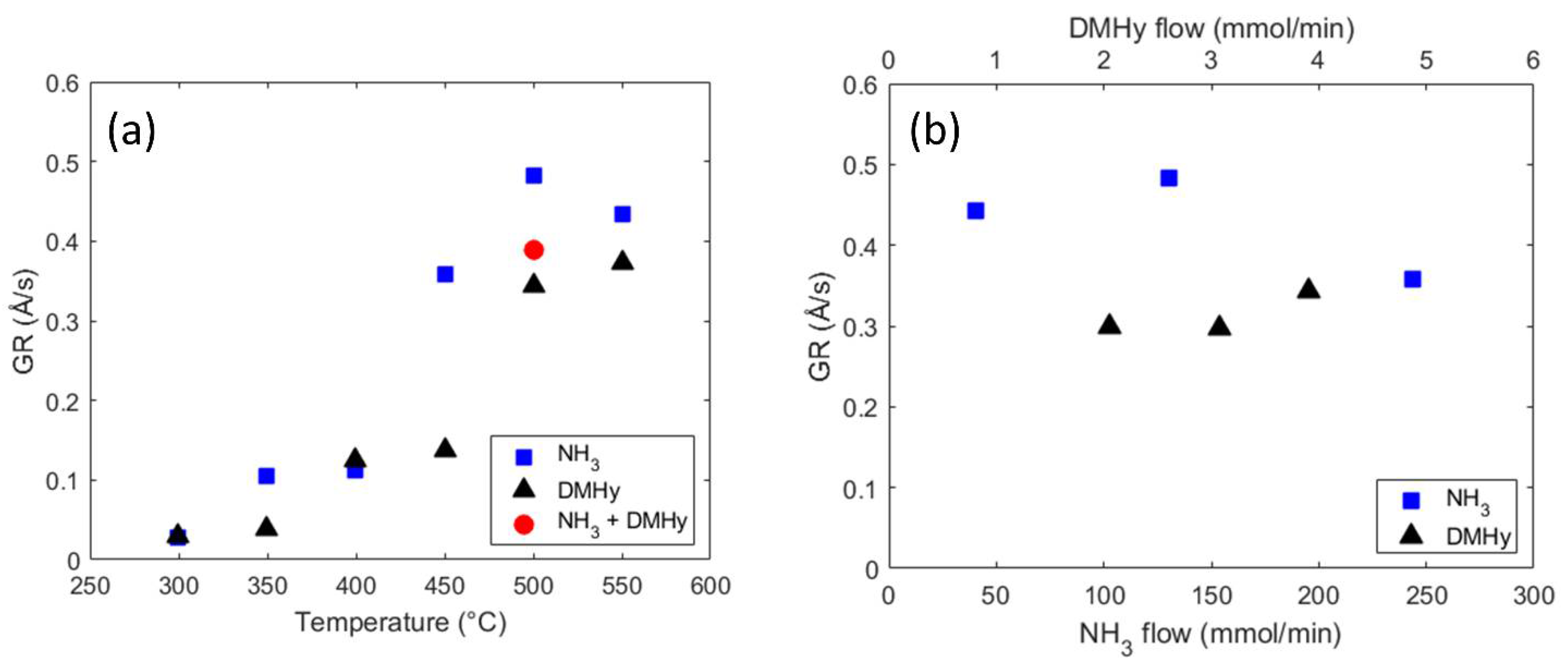
Figure 1a shows the growth rate (GR) versus growth temperature data for GaN grown with either NH
3, DMHy, or a mixture of the two N-precursors, calibrated through continuous growth on silicon. NH
3 and DMHy both showed significant growth in the 500 to 550 °C temperature range. At 500 °C, growth was also conducted with a combination of N-precursors and the GR was close to that seen for the film grown with DMHy alone. At lower temperatures the GR with both precursors decreased, with the GR with DMHy dropping significantly below 500 °C whereas the GR with NH
3 declined considerably below 450 °C. The difference in the temperature at which the growth rate decreased may be associated with the presence of methyl groups during growth with DMHy. The methyl groups of the DMHy can exchange with the ethyl groups of the TEGa, leading to formation of Ga-methyl bonds, such that the benefits of a lower pyrolysis temperature of TEGa compared to TMGa may have been partially lost [
29,
30]. Further investigations are needed to clarify the mechanism. Very little growth was seen with DMHy below 400 °C and with NH
3 below 350 °C. In
Figure 1b, the GR is plotted versus the N-precursor flow for samples grown at 500 °C with varying NH
3 or DMHy flows. The GR with DMHy was largely constant over the measured range, while the GR with NH
3 decreased slightly at the highest explored NH
3 flow of 250 mmol/min. Despite the large difference in N-precursor flow rates, the GRs being comparable suggested that the lower decomposition efficiency of NH
3 compared to DMHy could be compensated by providing significantly higher NH
3 than DMHy molar flows, and that the growth rate was largely determined by the TEGa flow in the range of the studied N-precursor flows.
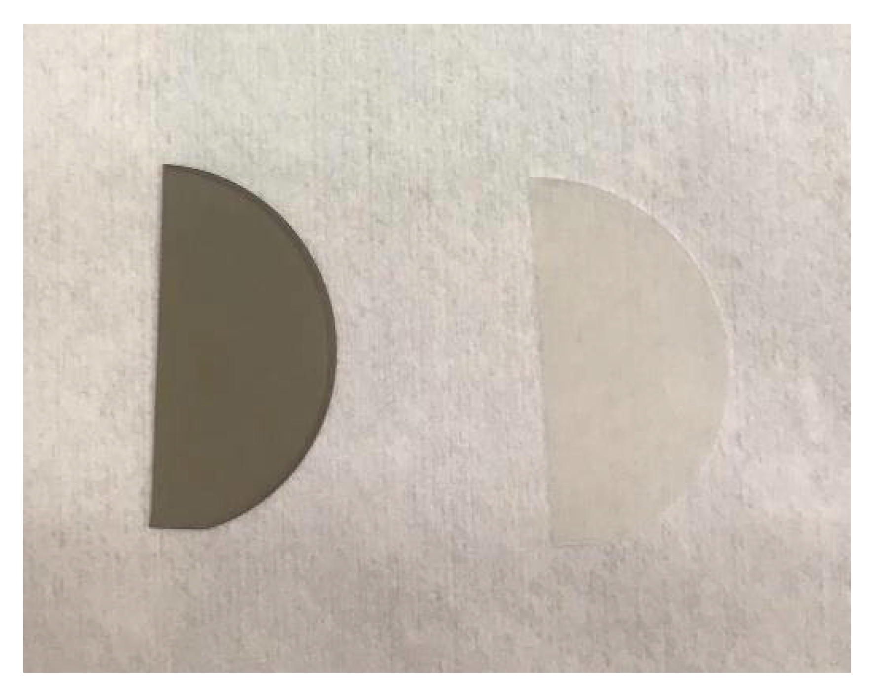
Selected samples from the GR calibration series were additionally grown directly on sapphire substrates. For growth with NH
3, samples were colorless as expected, however GaN films grown with DMHy were dark in color (
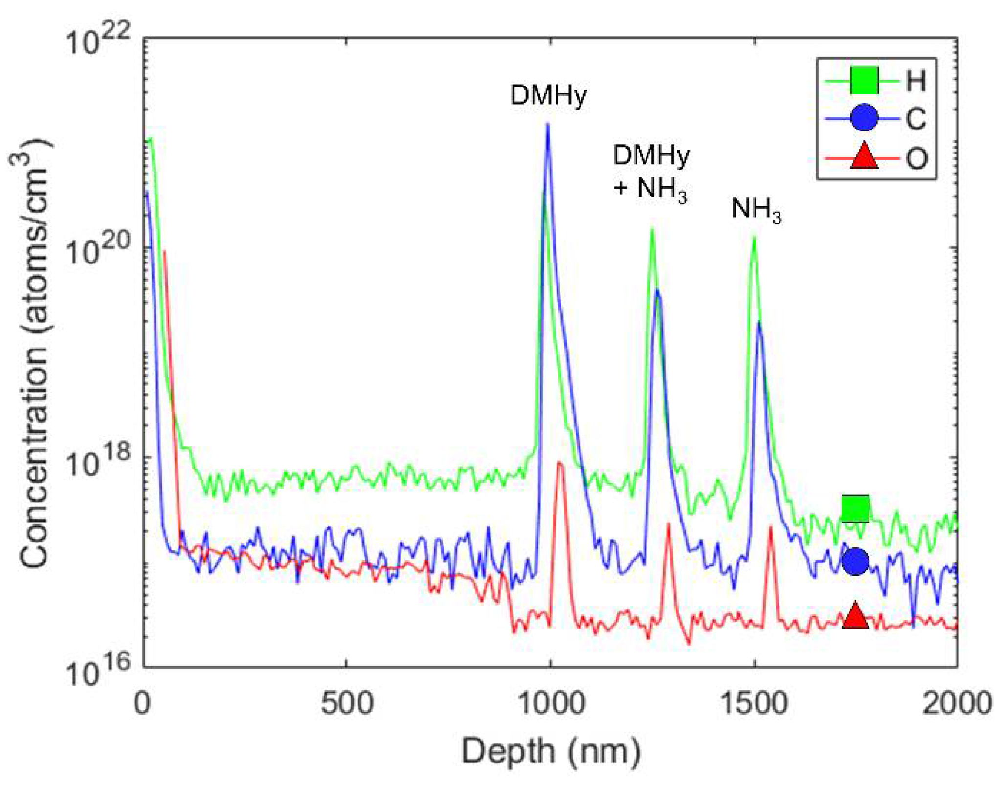
Figure 2). This effect was attributed to the formation of metal droplets due to the lower partial pressure of active nitrogen when growing with DMHy (lower V/III ratio) in combination with high levels of impurities in the films. To further investigate the latter, a sample was grown which consisted of LT GaN layers separated and capped by high temperature GaN. SIMS was conducted on this sample to determine the hydrogen, carbon, and oxygen impurity concentrations in the layers (
Figure 3). All LT layers were grown continuously at 550 °C and were therefore expected to have higher impurity levels compared to layer grown in FME mode. To determine impurity concentrations, the SIMS peaks were integrated and divided by the expected layer thicknesses, assuming 12.3 nm for each (
Table 2). It was seen that layer S1, grown with NH
3, had the lowest carbon level of 3 × 10
19 cm
−3 and S2, grown with a combination of N-precursors, exhibited a carbon concentration of 8 × 10
19 cm
−3, over twice the carbon content of S1. The carbon level in layer S3, grown with only DMHy, amounted to 2 × 10
21 cm
−3 and was nearly two orders of magnitude higher than that of layer S1. Oxygen levels in layers S1 and S2 were 7 × 10
17 cm
−3 and 9 × 10
17 cm
−3, respectively, significantly lower than the three times higher oxygen level in layer S3 of 3 × 10
18 cm
−3.
This indicated that carbon or oxygen may have been responsible for the dark color noted in previous samples grown with DMHy. The reduction of carbon going from S3 to S2 may be attributed to the better extraction of methyl groups from the DMHy with the presence of hydrogen provided by the NH
3, although additional carbon was still introduced by the DMHy in the case of S2 as compared to S1. The methyl groups provided by the DMHy precursors allowed the formation of Ga-methyl bonds on the growth surface, resulting in an enhanced C incorporation and impeding the advantages of using TEGa as precursor, which normally allows the growth of LT films with lower C impurity concentrations compared to TMGa, due to the easier cleavage of the Ga-ethyl compared to the Ga-methyl bond [
29]. The relatively low oxygen level in S2 shows that the oxygen contamination could be suppressed by the addition of NH
3, suggesting that the high O concentration in the GaN layer grown with DMHy alone (S3) was in part associated again with the significantly lower N-precursor partial pressure which was limited by the vapor pressure of DMHy.
When performed on high temperature GaN base layers, it was shown that LT FME GaN growth conducted at 550 °C with NH
3 could result in a step-flow growth mode with low surface roughness [
20]. When FME GaN was grown with DMHy on top of high temperature GaN (sample G1), AFM micrographs revealed rough films with features above 400 nm tall. These features may have been formed via metal-droplet assisted nanowire formation due to the low V/III ratios when growing with DMHy. Due to the successful growth of GaN with NH
3 under similar conditions, NH
3 was chosen as the N-precursor of choice for LT GaN growth moving forward.
DMHy and NH
3 were then compared as N-precursors for LT AlN growth. Despite concerns with DMHy for use in GaN growth, the growth of AlN with DMHy was expected to benefit from the lower N-precursor partial pressure due to the higher stability of AlN compared to GaN leading to lower V/III ratios being necessary for growth [
31]. In addition, known pre-reactions between NH
3 and TMAl make finding an alternative N-precursor attractive.
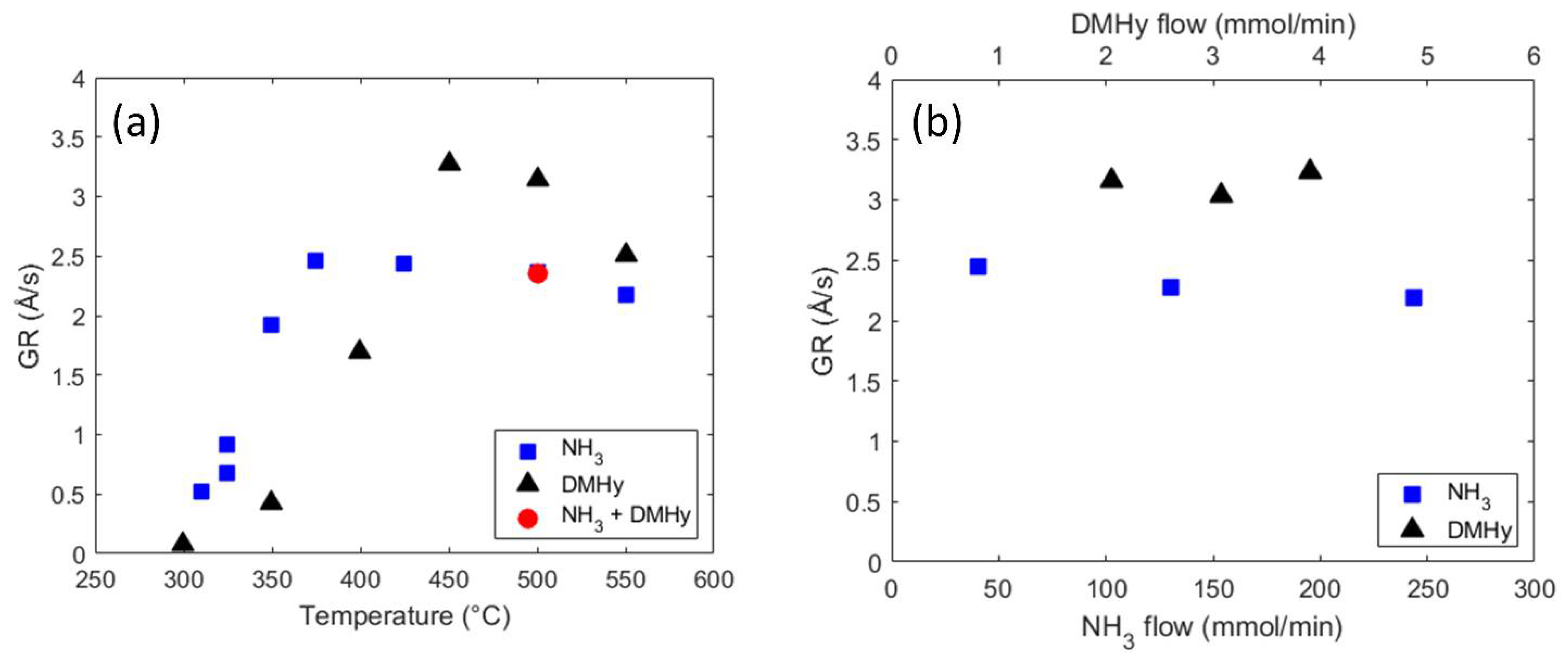
Figure 4 shows the GR versus temperature and GR versus N-precursor flow plots for AlN grown continuously on silicon. Unlike in the case of GaN growth, AlN growth with DMHy showed a higher GR than with NH
3 at temperatures of 450 °C and higher (
Figure 4a), most likely due to the pre-reactions between NH
3 and TMAl limiting the AlN GR. The AlN films grown with both N-precursors present at 500 °C was seen to match the GR of NH
3 alone, again most likely due to pre-reactions effectively reducing the available TMAl. At temperatures below 450 °C the GR with DMHy decreased and was seen to be lower than that with NH
3. In comparison to previously studied growth with TEGa, the GR with DMHy remained high at somewhat lower temperatures due to the high pyrolysis of TMAl. Instead of being related to the group III precursor, the GR decrease with decreasing temperature was attributed to the decreased cracking efficiency of DMHy which was previously observed to occur in this temperature range [
32]. While DMHy exhibited effectively no AlN growth at 300 °C, the growth of AlN with NH
3 was still appreciable down to these temperatures, although greatly reduced. This decrease in GR with the use of NH
3 was likely a factor of the lower TMAl pyrolysis below 350 °C [
33]. For N-precursor variation studies conducted at 500 °C (
Figure 4b), the GR with DMHy was seen to be constant over the measured range, while the AlN GR with NH
3 decreased slowly as more NH
3 was available to cause pre-reactions with TMAl. As the targeted growth temperatures in this study were between 500 °C and 550 °C, the growth at the lower temperatures was not further studied.
LT FME AlN was then grown on high temperature GaN using either DMHy (A1) or NH
3 (A2). A third sample was grown which consisted of LT FME AlN on LT FME GaN on high temperature GaN, all grown with NH
3 (A3).
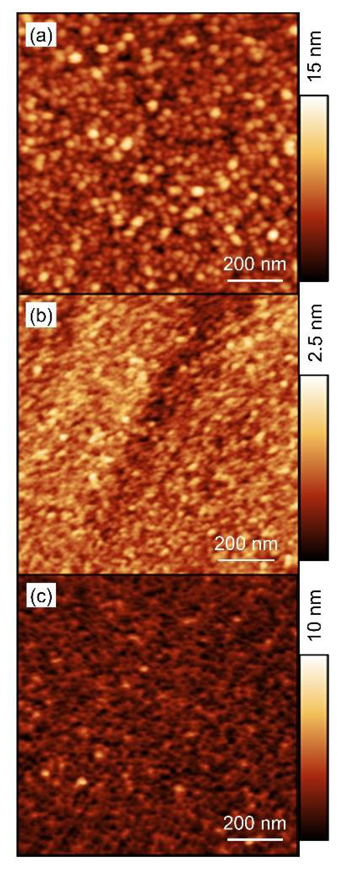
Figure 5 shows AFM micrographs of these three samples. All samples exhibited a layer-by-layer growth mode unlike the step flow growth observed for FME GaN with NH
3. While the LT FME AlN layer grown with NH
3 (sample A2) had a very smooth surface with a root mean square roughness of 304 pm, sample A1 grown with DMHy was significantly rougher with a root mean square of 1.84 nm. Sample A3, where the LT FME AlN layer had been grown on top of a thin LT GaN layer, exhibited a surface roughness of 770 pm. Optimization of the flow scheme via changing flow rates and times may serve to decrease these roughness values further, however that was outside of the scope of this work. The differences in morphology between A2 and A3 indicate that the LT GaN layer, despite its step-flow growth with good morphology, affected the growth mode of the LT AlN layer on top. The smaller step length on the surface of the LT GaN film as compared to the high temperature GaN film was likely responsible for the increased roughness of sample A3.
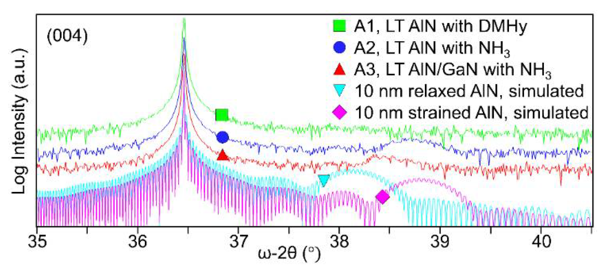
To gain information on the strain state and crystallinity of the LT AlN layers, XRD ω-2θ scans were conducted on the (004) GaN peak,
Figure 6. Simulations of strained and relaxed layers of AlN on GaN were compared to the experimental scans. For sample A1, AlN grown with DMHy, little to no peak associated with AlN could be seen in the XRD scan. In contrast, sample A2 grown with NH
3 showed a strong AlN related peak that was only slightly shifted from that expected for fully strained AlN. The small shift of the AlN peak towards the GaN peak could be due to some slight Ga incorporation, slight relaxation, or a combination of these effects. Note that the observed shift of the AlN peak in sample A2 was much less than in previous work, where a significantly larger shift of the AlN towards the GaN peak was observed, caused by Ga incorporation into the AlN films [
18]. Fringe peaks were visible on either side of the A2 AlN peak corresponding to a thickness of 10 nm. For sample A3, an asymmetric peak attributed to AlN was visible between that of the strained and relaxed AlN reflections. Similar to the A2 case, this may have been due to some Ga incorporation, relaxation, or both.
Hall measurements were conducted on samples A1, A2, and A3 to determine the characteristics of 2DEGs which were expected to form at their GaN/AlN interfaces. Sample A1 with AlN grown with DMHy was resistive and no 2DEG was measured. As the XRD data for this sample showed no measurable AlN peak and AFM showed a very rough film, most likely the AlN was polycrystalline in nature and therefore no 2DEG would form due to the lack of polarization. For samples A2 and A3, both grown with NH
3, Hall measurements confirmed the presence of 2DEGs. For sample A2 composed of LT AlN on high temperature GaN an electron mobility (μ) of 540 cm
2/V∙s and a sheet charge (n
s) of 3.76 × 10
13 cm
−2 were measured, on par with results reported for AlN/GaN heterostructures grown by MBE [
11,
12,
13]. Despite the LT growth of the AlN layer, a high charge and mobility were obtained as the AlN was strained with high crystallinity. The properties of sample A2 were superior to those of the samples in our previous study, where unintentional Ga incorporation into the AlN layers was observed [
20]. Sample A3, where a LT GaN layer was inserted underneath the LT AlN, exhibited an electron mobility of 230 cm
2/V∙s and a sheet charge of 1.59 × 10
13 cm
−2 (
Table 3). The causes leading to the different position and shape of the AlN XRD peak for this sample compared to sample A2, potential Ga incorporation and/or partial relaxation, are most likely also responsible for its reduced sheet charge. Compensating defects in the LT GaN layer, which was known to contain higher C and O impurity concentrations compared to high temperature GaN, may have contributed as well [
20]. The reduction in mobility was most likely caused by an increase in interface roughness associated with a smaller step length on the LT GaN as compared to the high temperature GaN surface prior to AlN growth [
34]. The elevated impurity levels in the LT GaN layer in sample A3 may have also contributed.
To further explain the difference between growth with DMHy versus NH
3, LT AlN/GaN samples were studied with TEM.
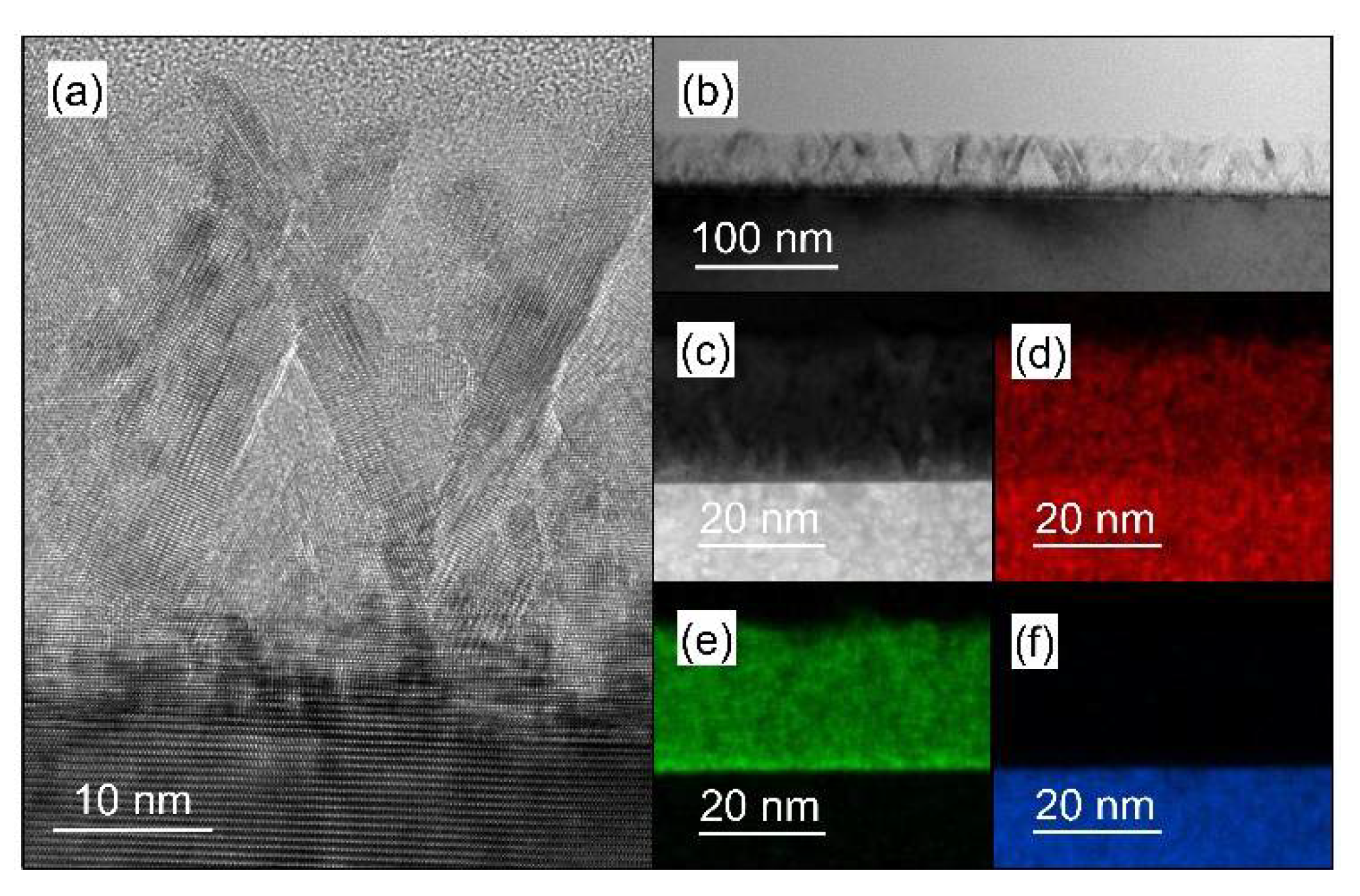
Figure 7 shows TEM cross-sections for sample Al, where the AlN layer was grown with DMHy. TEM results showed an AlN layer which was polycrystalline past the first few nanometers and had a rough surface consistent with that seen via AFM. The polycrystalline nature visible via TEM supported the lack of an AlN XRD peak and was consistent with the lack of 2DEG formation found via Hall measurements. From EDX measurements, it was seen that no significant Ga incorporation occurred in the LT AlN layer, with a compositionally sharp interface. Some Al enrichment was seen at the interface, in the area where the film showed reasonable crystallinity.
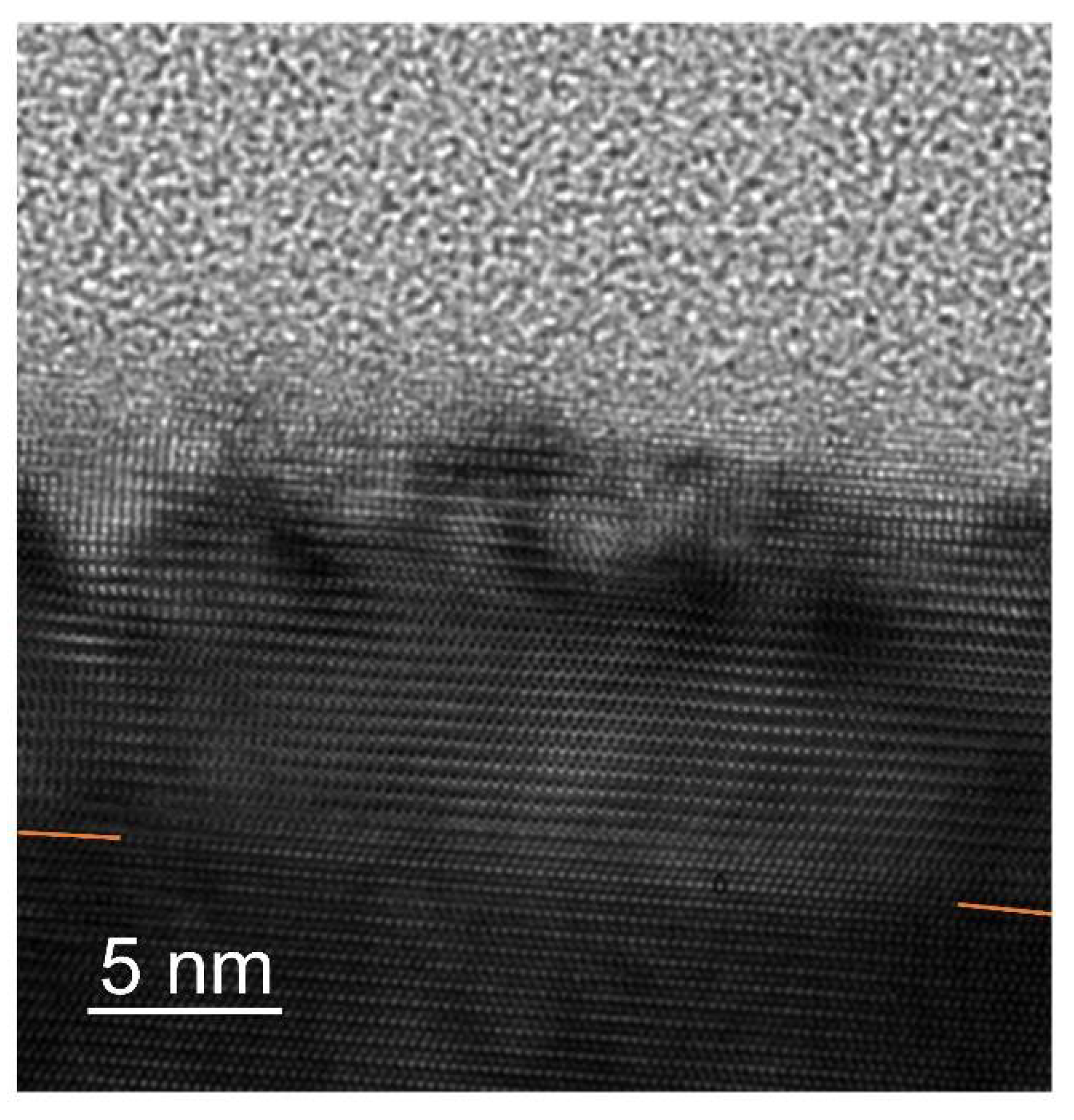
Sample A2, where the AlN layer was grown with NH
3, exhibited higher AlN crystallinity and a lower surface roughness than A1 (
Figure 8). This TEM result was consistent with XRD, Hall, and AFM measurements. From the XRD results it was already known that there was insignificant Ga incorporation. The absence of unintentional Ga incorporation in the AlN layers in this study was most likely due to a relatively clean growth chamber reducing the effects of Ga evaporations from GaN deposits in the chamber. The high crystallinity of the LT FME AlN layers grown with NH
3 enabled the demonstration of LT FME AlN/high temperature GaN 2DEGs with properties similar to those grown under standard growth conditions by MBE.


 ,
, 


