1. Introduction
Group III-nitride semiconductors have been extensively investigated because of their wide direct band gaps and superior thermodynamic properties [
1]. The energy gaps of GaN (3.43 eV), InN (0.64 eV), and AlN (6.14 eV) can cover the whole visible-light spectra [
2]. Therefore, InGaN alloy quantum wells (QWs) are widely applied in commercial light-emitting diodes (LEDs) nowadays [
3,
4]. However, the lattice mismatch and the strain between GaN and InGaN generates many structural defects and results in non-radiative recombination to degrade the device performance. Therefore, the efficient performance drop in yellow–red light wavelength discourages the application progress of group III-nitride semiconductors for the full visible-light spectrum [
5,
6]. Moreover, a high growth temperature induces indium decomposition, which causes many dislocations and defects [
7]. Large lattice misfits degrade the crystal quality and even generate structural cracks. The structural cracking considerably limits the quality of heterostructured QWs, and then reduces the performance in photon emission of LEDs [
8]. In the previous study, it was shown that there were no cracks occurring for a lattice misfit less than 1%, in which the lattice stress was under the linear elastic region of Hooke’s law [
9]. Therefore, an In
yAl
1−yN epi-layer will be a suitable barrier for an In
xGa
1−xN QW. By modulating the indium content (
y), the In
yAl
1−yN epi-layer matched to the lattice-constant of GaN was evaluated at the indium composition of
y ≈ 17.1% [
10].
Figure 1 shows the diagram of band-gap energy of III-nitrides versus lattice constants. The blue, green, and red dashed lines indicate the lattice-matched points of In
xGa
1−xN/In
yAl
1−yN QWs for blue, green, and red light emission, respectively [
11,
12]. The detailed energy gaps, indium contents, and lattice constants were calculated for upper (u) and lower (l) limits of blue, green, and red lights in
Table 1. For instance, in the upper limit of blue-light emission (line 1,
Table 1), the energy gap (e.g.,
Ex = 2.84 eV) in In
xGa
1−xN was converted to indium content (
x = 13.0%) by the bowing parameter modification (b = 1.9 for In
xGa
1−xN) [
12]. For the indium content (
x) of 13.0% in In
xGa
1−xN, its lattice constant
a can be calculated by Vegard’s law [
13], and this value (
a = 3.234 Å) will match 28.9% indium content (
y) of the In
yAl
1−yN barrier with an energy gap of
Ey = 4.12 eV (calculated by the bowing parameter with b = 2.1 for In
yAl
1−yN [
14]). The lattice-matched QW structures can reduce structural defects and increase radiative electron-hole recombination for superior device performance. Moreover, the large band-gap offset (Δ
Eg =
Ey −
Ex = 1.28 eV) of the In
xGa
1−xN/In
yAl
1−yN QW will provide a better quantum confinement effect and enhance the internal quantum efficiency. The lattice-matched In
xGa
1−xN/In
yAl
1−yN QWs for upper limit of green and red light emissions were also calculated with indium content
x = 19.9% and 33.9%, and
y = 34.6% and 46.0% (
Table 1), and they have the band-gap offsets of Δ
Eg = 1.20 and 1.04 eV, respectively. Therefore, the lattice matched hetero-structured QW can improve the quantum efficiency of devices and also extend the emission wavelength of GaN-based LEDs to the red-light region. In such a way, one can engineer the band profiles of III-nitrides (e.g., by the variation in alloy compositions,
x and
y, in
Figure 1) to design, theoretically, hetero-structured epi-layers for a specific optoelectronic device; this is the so-called “band engineering technique” of a QW.
The growth of high quality InAlN epi-layer with a high indium concentration is regarded as a challenge, owing to the occurrences of strain effect, indium decomposition [
15], phase separation, and indium droplet accumulation at a growth temperature of ~630 °C or higher [
2]. However, a relative high growth temperature (i.e., 630 °C) is necessary for an improvement in its optical characteristics. One way to solve the problem is to reduce the growth duration at high temperature and limit the effect of indium decomposition. The stacking faults of decomposition can be minimized by reducing the growth duration at high temperature. Moreover, the less indium decomposition enhances the effect of indium incorporation, which is in favor of the growth of the In
yAl
1−yN barrier. On the other hand, the metal modulation epitaxy was also performed to release the strain effect and obtained good quality and uniformity [
16]. In this paper, we apply the lattice-matched band engineering technique to demonstrate the growth of a large band-gap-offset In
xGa
1−xN/In
yAl
1−yN QW for the application of full-color light-emitting diodes.
2. Materials and Methods
GaN/In
xGa
1−xN/In
yAl
1−yN QWs were grown on 4.5 μm thick
c-plane GaN templates by using the Veeco Applied-GEN 930 plasma-assisted molecular beam epitaxy (PA-MBE) system. The GaN templates were pre-grown on a patterned sapphire substrate by metal organic chemical vapor deposition. Before the MBE growth, the GaN template substrates were ultrasonically cleaned in acetone (5 min), isopropanol (5 min), and de-ionized water (5 min) and sequentially dried by nitrogen gas. Thermal cleaning was performed in load-lock and buffer chambers at 180 and 550 °C, respectively. Then, the substrate was sent to the MBE growth chamber for outgassing at 800 °C for 10 min and cooled to the growth temperature for the first initial epi-layer. The PA-MBE system was equipped with a radio-frequency plasma nitrogen source of 6 N purity, and standard Knudsen cells for gallium, aluminum, and indium of 9 N purity. The detailed equipment and growth procedure can be accessed in our previous research [
4,
6]. In the whole growth procedure, the metal modulation epitaxy was performed to yield a desirable crystal quality [
16]. First, the GaN epi-layer was grown with 18 s Ga-wetting layer and 10 s N-treatment at 770 °C, and the gallium and nitrogen treatments were repeated for 24 cycles. The growth temperature was ramped to 730 °C for In
xGa
1−xN QW with 10 s InGaN flux and 12 s nitrogen treatment for 5 cycles. After the growth of InGaN QW, the samples were ramped to 630 °C right away at a cooling rate of 10 °C/min. Finally, 10 s InAl wetting layer and 15 s nitrogen treatment were repeated for 35 cycles at 630 °C. After the growth procedure, different thermal treatments were carried out immediately in the MBE chamber for the samples studied here. Sample A was annealed at 630 °C for 3 min in the MBE growth chamber and ramped down to room temperature at a cooling rate of 10 °C/min. For other samples, the annealing procedures were canceled, and the cooling rate was modulated from 10, 20, to 40 °C/min (denoted as samples B–D, respectively). A scanning electric microscope (SEM, JOEL-6700) with an accelerated voltage of 10 kV was used to inspect the surface morphology of the samples. The crystalline property was analyzed by X-ray diffraction (XRD) measurements using the Cu K
α line (λ = 1.5406 Å) as an X-ray source. In the surface chemical composition measurements, X-ray photoelectric spectroscopy (XPS/ultraviolet photoelectron spectroscopy system, PREVAC) was used with a monochromatic aluminum (Al) K
α X-ray source (1486.6 eV) and a hemispherical analyzer operating in the Constant Analyze Energy mode (survey: 200 eV). Surface charging effect was compensated by using an Ar
+ gun and the energy was calibrated with the C1s peak position at 284.8 eV. The interface atomic structures of the samples with a zone axis of [11
0] were characterized by a high-resolution transmission electron microscope (HR-TEM, Philips Techni F-20) with an acceleration voltage of 200 kV. The HR-TEM specimens were prepared by a dual-beam focus ion beam (FIB, Hitachi HR2000).
3. Results and Discussion
Four samples of In
xGa
1−xN/In
yAl
1−yN epi-layers with different cooling processes in MBE growth were used to study the characteristics of lattice-matched and large band-gap offset In
xGa
1−xN/In
yAl
1−yN QW. The inset of
Figure 2 shows the schematic of GaN/In
xGa
1−xN/In
yAl
1−yN QW. In
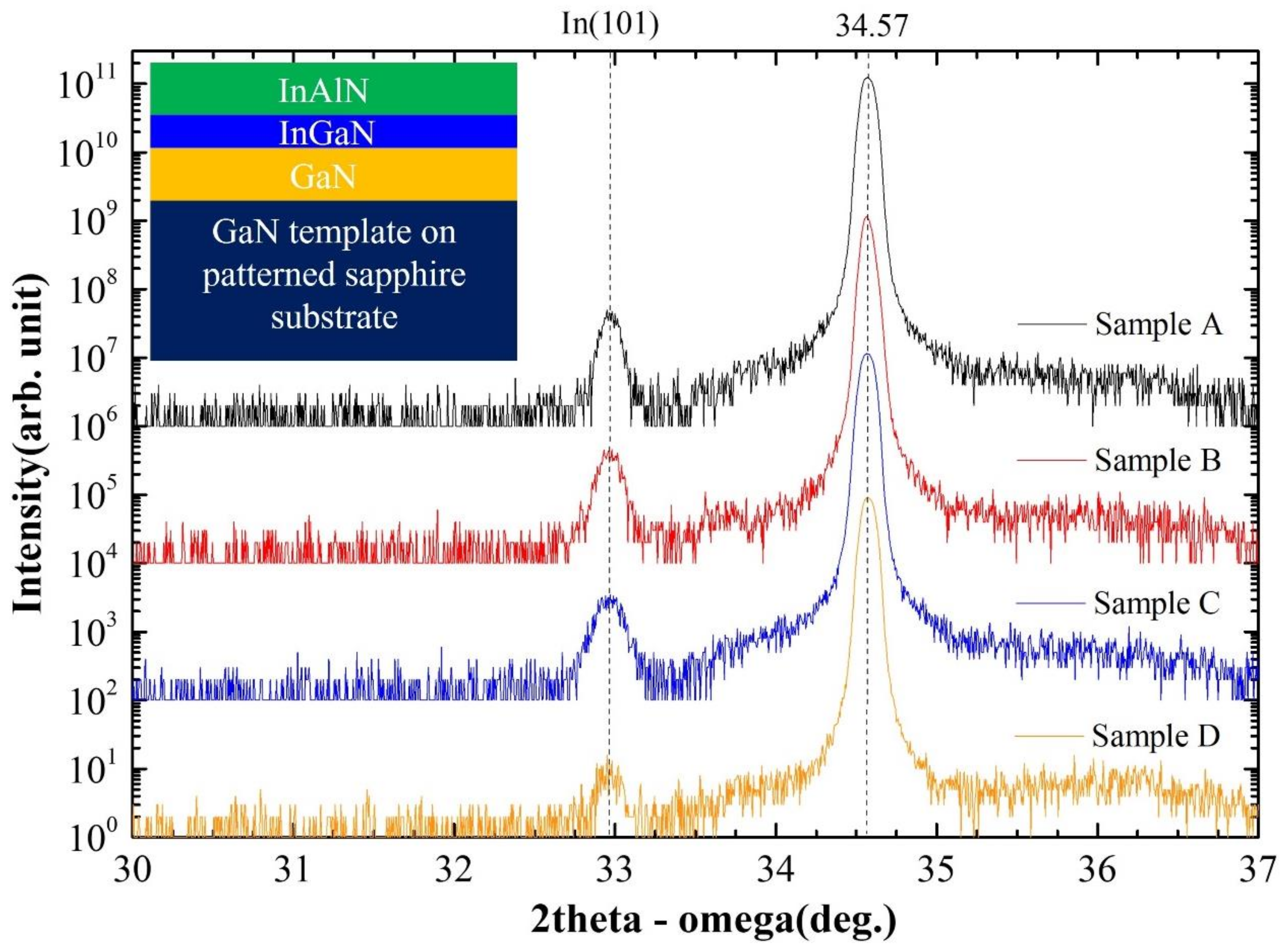
Figure 2, the peaks at 34.57° were associated with GaN template, and those around 32.96° were contributed by the indium (101) plane. When the growth duration of the InGaN layer and InAlN barrier had 5 and 35 cycles, respectively, their thickness may be out of the resolution of XRD detector. Therefore, no apparent signals of InGaN or InAlN were observed in the XRD measurements. The intensities of the indium (101) plane were 50, 40, 32, and 16 for samples A, B, C, and D, respectively. The indium composition effect was notably significant in sample A with an annealing duration of 3 min and a 10 °C/min cooling rate. When the annealing process was canceled in sample B, the indium composition effect was suppressed, and the intensity of the indium (101) plane decreased to 40. In samples C and D, the cooling rate increased to 20 and 40 °C/min, respectively, resulting in the further suppression of indium composition, and the intensity of the indium (101) plane decreased to 32 and 16, expectedly.
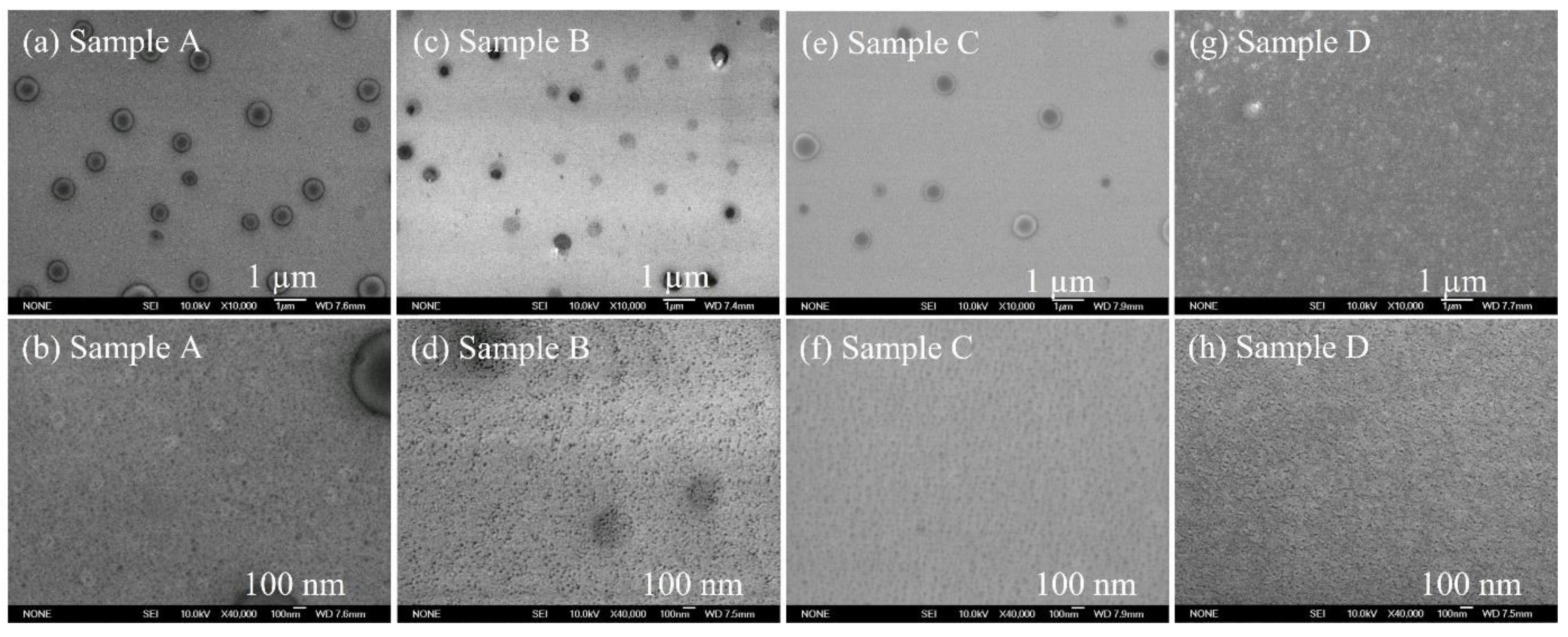
Figure 3 depicts the SEM images at different magnifications. The indium droplets were diminished with the annealing cancelation (
Figure 3a vs.
Figure 3c) at 10,000× magnification. Moreover, the indium droplets exhibited a light-colored morphology in the comparison of their lightness at high magnification (
Figure 3b vs.
Figure 3d). This result indicates that the indium droplets were thicker in sample B after annealing cancelation. In consideration of the surface morphology, samples A and B were roughly smooth; the white circles and black dots represent the phase separation of Al-rich and In-rich parts in the In
yAl
1−yN layer, respectively [
17,
18]. In samples C and D, the indium droplets were further diminished by increasing the cooling rate (
Figure 3e,g). The decreasing results of indium droplets were consistent with the XRD measurements in
Figure 2. As the cooling rate increased to 40 °C/min, the indium droplets can be hardly found in
Figure 3g. At higher magnification, samples C and D revealed a smooth and distinct surface morphology (
Figure 3f,h) in comparison with samples A and B.
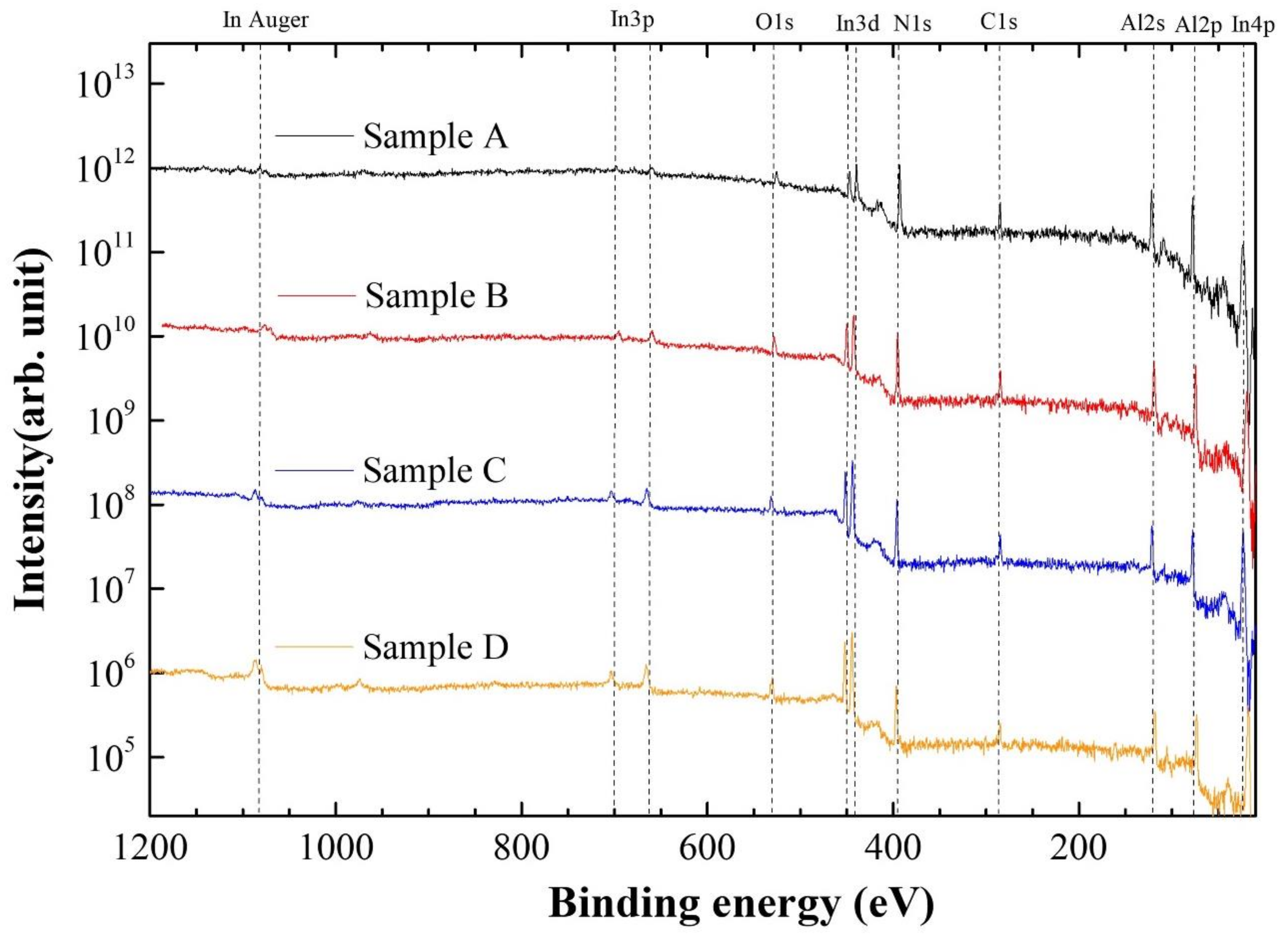
XPS measurements were performed to evaluate the indium composition and investigate the influence of the thermal process on indium incorporation. The results are plotted in
Figure 4. The atomic ratio in XPS measurements was calculated by the integrated area of the element peaks and modified with Relative Sensitivity Factors in “CASA XPS version 2.3.23.” software, provided by PREVAC, Inc. The capture depth of excitation photoelectron in the XPS system was less than 10 nm. Therefore, the elements in the XPS spectra were all contributed by the InAlN layer. The signals of main chemical elements, aluminum (Al), indium (In), and nitrogen (N) can be found in the spectra. In addition, several minor elements, such as carbon (C) and oxygen (O) were detected as well. These peaks were associated with the adventitious carbon sticking and oxidation in the air atmosphere [
19,
20]. The organized elements proportion for samples A, B, C, and D are listed in
Table 2 lines 1–5, with a standard deviation of less than 0.2 at %. In3d and Al2p were selected as the main contributions, which were derived and sorted out in line 6 (
Table 2), to calculate the indium composition of the In
yAl
1−yN barrier. The indium composition increased as the annealing procedure was halted, and the indium fraction increased from 10.11% to 18.95%. In samples C and D, the indium composition further increased to 25.9% and 32.23% with the accelerated cooling rate in the growth procedure, respectively. Therefore, we suspended the annealing to avoid indium decomposition at a relatively high growth temperature, and accelerated the cooling rate, which enhanced the indium incorporation. These results showed good agreement with the analyses of SEM images and XRD measurements.
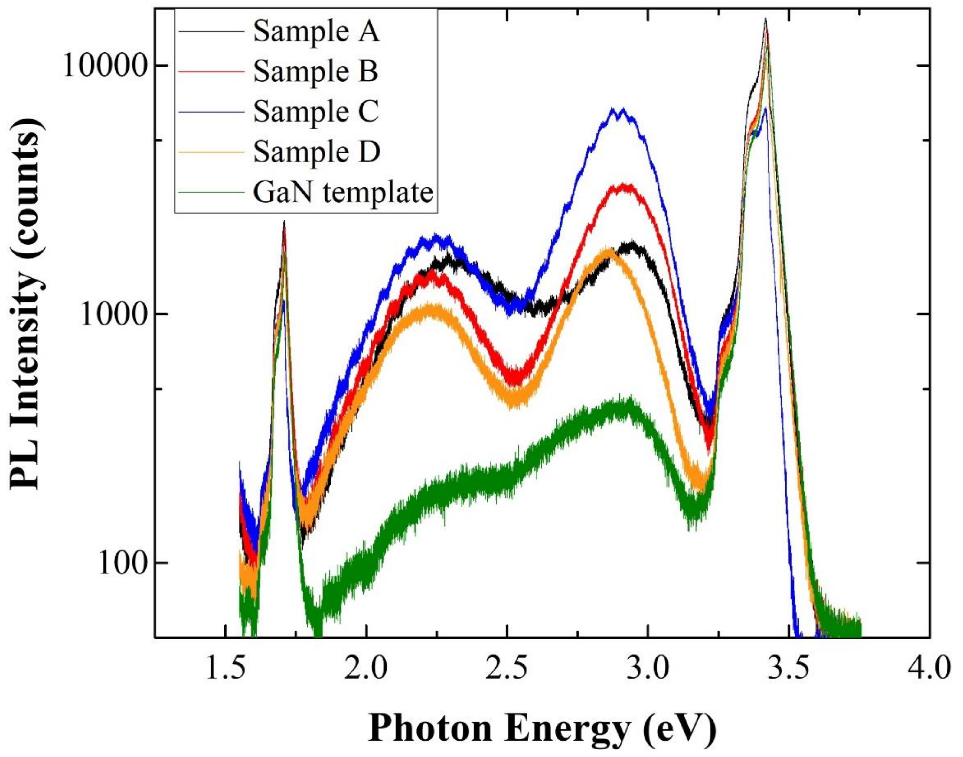
To check the band gap energy, we performed photoluminescence (PL) measurements on all the samples at room temperature, and the results are presented in
Figure 5. The GaN template was also used as a background signal, and it was plotted by a green line in
Figure 5. By nonlinear curve fitting of the packet near 3.4 eV to Gaussian functions for all the samples, we obtained three peaks. The peaks near 3.43 eV were the contribution from the GaN template for all the samples. The shoulders near 3.37 and 3.27 eV were attributed to the basal stacking faults [
21] and the transition of donor–acceptor pairs [
22] in the GaN template, respectively. The GaN/In
xGa
1−xN/In
yAl
1−yN QW was associated with the peaks of 2.92, 2.90, 2.89, and 2.85 eV for samples A, B, C, and D, respectively. The intensities changed with different thermal treatments. As listed in
Table 3, the intensities of QW emission increased from 1908 to 3351 counts in samples A and B, indicating that the optical property was enhanced when the annealing was diminished. It was found that the suppression of indium decomposition increased the epi-layer quality at the InGaN/InAlN interface; resulting in the efficiency of recombination. Moreover, sample C exhibited the strongest QW intensity of 6688, because of the acceleration of cooling rate as well as the cancelation of annealing. On the other hand, the intensity of sample D was 1856, resulting from the difference in thermal expansion coefficient of InAlN and GaN at a high cooling rate [
23]. Moreover, the full width at half maximum (FWHM) of InGaN QWs for sample A–D showed a consistent result with the PL intensities. Sample A had the poorest FWHM of (0.68 ± 0.007) eV because of indium decomposition during the annealing procedure. In sample B, the FWHM improved to (0.31 ± 0.005) eV by canceling annealing, and we obtained the best FWHM of (0.26 ± 0.002) eV in sample C because the indium decomposition was further suppressed by the increase in cooling rate. The decrease in FWHM to (0.31 ± 0.005) eV in sample D was caused by the difference in the thermal expansion coefficient of InAlN and GaN at a relatively high cooling rate. These FWHM analyses are consistent with the intensities and XRD findings. To calculate the indium composition in the InGaN QWs, we used the bowing parameter of InGaN to approach the accurate values; the formula for bulk In
xGa
1−xN is given by E
g(x) = [3.43 − 2.79 × (x) − 1.9 × (1 − x) × (x)] eV [
24]. We estimated the content of indium in In
xGa
1−xN at 11.4%, 11.9%, 12.1%, and 13.1% for samples A, B, C, and D, respectively. The peaks near 2.25 eV contributed to the bandgap transitions or structural defect levels emitted from In
xGa
1−xN/GaN layers or GaN template [
25]. The peaks near 1.7 eV for all samples were associated with the second harmonic signal of GaN template (3.4 eV).
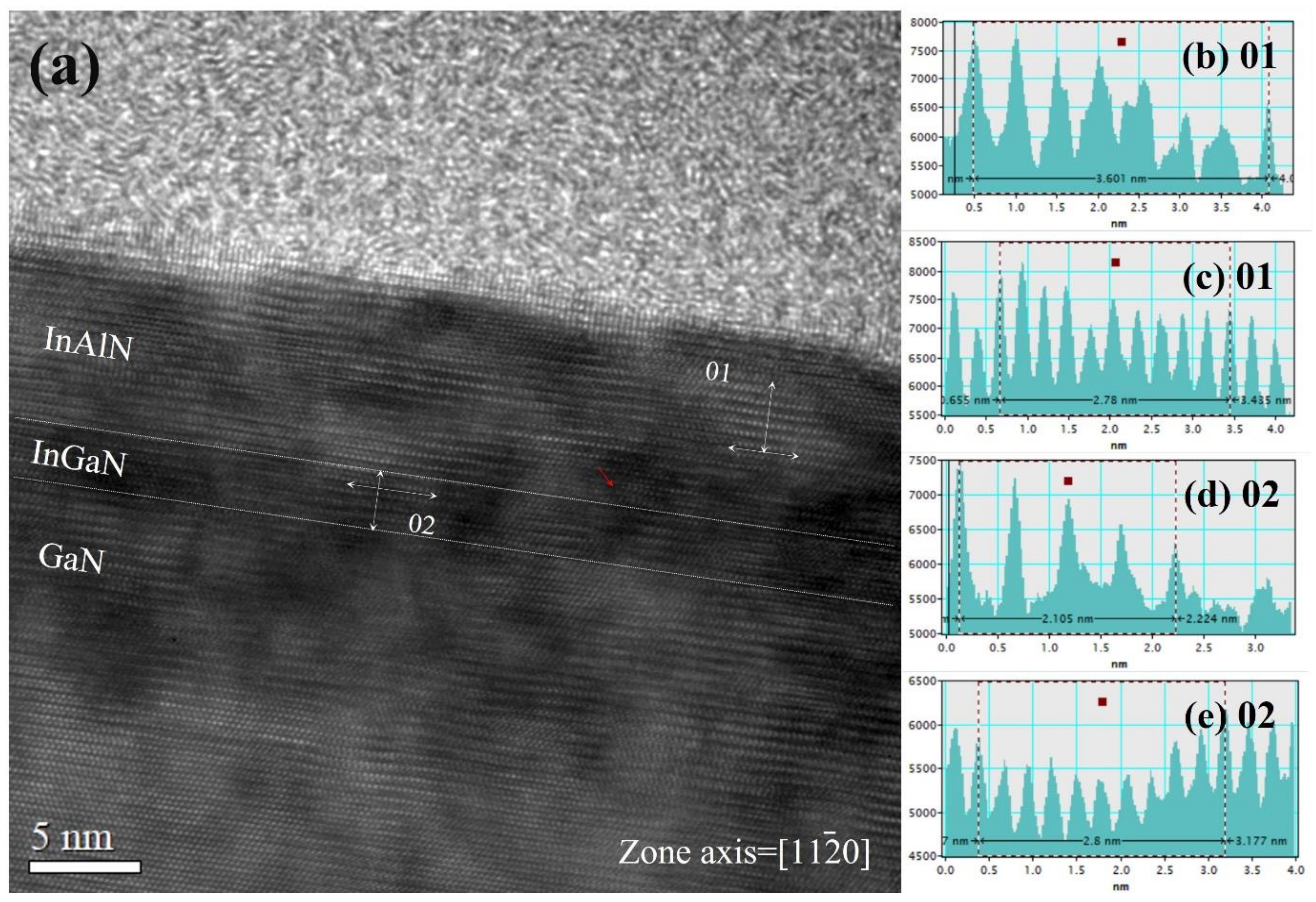
Finally, to confirm the lattice constant and material structure of GaN/In
xGa
1−xN/In
yAl
1−yN QW, we selected sample C to perform TEM measurements because of its best optical property. We prepared the TEM specimen along the [11
0] zone axis. As shown in the HR-TEM image of
Figure 6a, the layer of InGaN was simply differentiated by the two dashed lines. The region above InGaN was denoted as the InAlN layer, and the lower region was denoted as the GaN template. A roughly distinct atom arrangement was observed, and a limited number of defects were detected in the InGaN QW or InAlN barrier in spite of several dislocations at the InGaN/InAlN interface, as pointed out by the red arrow in
Figure 6a. We used atomic layer measurement in the internal software “DigitalMicrograph” provided by Tecnai, Inc. to determine the
d-spacing of the InGaN and InAlN layers. As presented in
Figure 6a, we selected position 01 in the InAlN barrier and position 02 in the InGaN QW to measure the atomic layer because of the reduced damage and remarkable layer arrangement. The [0002] (
dc) and [1
00] planes (
dM) of InGaN/InAlN were measured, and the results are summarized in
Table 4. For position 01 in the InAlN barrier, we measured the atomic layer along the [0002] direction for seven periods and the length was 3.601 nm. The average
dc was 5.142 Å. In the [1
00] direction, 10 periods of atomic layers were measured with a length of 2.78 nm, and the average
dM was 2.78 Å. For position 02 in the InGaN QW, we measured the atomic layer along the [0002] direction for four periods, the length was 2.105 nm, and the average
dc was 5.262 Å. In the [1
00] direction, 10 periods of atomic layers were measured with a length of 2.80 nm, and the average
dM was 2.80 Å. The indium composition of In
xGa
1−xN and In
yAl
1−yN in sample C can be estimated by Vegard’s law [
13], resulting in the indium content of 22.5% in In
yAl
1−yN and 14.8% in In
xGa
1−xN. The indium content in In
yAl
1−yN calculated by HR-TEM (22.5%) was roughly consistent with the results of XPS measurement (25.9%). The indium content In
xGa
1−xN calculated by HR-TEM (14.8%) was consistent with the estimation in PL measurement (12.1%). Therefore, the peaks near 2.25 eV in the PL spectra were attributed to structural defect levels emitted from In
xGa
1−xN/GaN or the GaN template, rather than the InGaN QW. Finally, the lattice mismatch between In
xGa
1−xN and In
yAl
1−yN can be derived by the average atomic layer in the [1
00] direction, i.e., the deviation between In
xGa
1−xN (
dM) and In
yAl
1−yN (
dM) was 0.71%. The low lattice mismatch (0.71%) between In
xGa
1−xN and In
yAl
1−yN agrees with the designed lattice-matched QWs.


