1. Introduction
No doubt, high structural quality gallium nitride (GaN) substrates are required for building a new generation of electronic and optoelectronic devices such as transistors or laser diodes [
1,
2]. One of the most promising technologies for crystallizing GaN is the ammonothermal method [
3,
4,
5,
6,
7,
8,
9,
10,
11,
12]. It involves dissolving the feedstock material (mainly GaN polycrystals) in ammonia (NH
3) in one zone of an ammonothermal autoclave and convective transport of the dissolved material to the second zone with native seeds where the crystal growth takes place. The crystallization process runs at NH
3 pressure of 300–600 MPa and temperature in the range of 300–750 °C [
3]. In order to increase the feedstock solubility, some mineralizers such as alkali metals or halide compounds are applied. Two ammonothermal growth methods can be, respectively, distinguished: basic and acidic [
13]. In the case of the basic ammonothermal crystallization process, GaN crystals (Am-GaN) of the highest structural quality can be obtained [
14,
15,
16,
17]. They are crystallographically flat with bowing radii of crystallographic planes higher than 15 m for a 2-inch crystal or wafer and with a low, of the order of 5 × 10
4 cm
−2, threading dislocation density (TDD). Depending on dopants and getters applied, highly conductive (n-type) or semi-insulating (SI) crystals can be grown. Two-inch Am-GaN substrates are available on the market [
18].
In spite of the very high structural quality of the Am-GaN crystals, there is still room for their improvement. Recently, it was reported that the etch pit density (EPD; correlated with TDD) is two orders of magnitude lower in parts of crystals grown laterally (in the [11-20] crystallographic direction) than in the area grown in the [000-1] crystallographic direction [
19]. Higher EPD in the central part of Am-GaN was combined with some stress existing in the crystals. This stress, visible in cross-polarized light, was called the stress-induced polarization effect (SIPE). It was stated that SIPE could appear on part or the entire surface of the crystal except for its laterally grown parts [
15,
19].
The process of the SIPE formation still remains an open question. It seems that it appears at the beginning of the growth process. At this point, the convective transport of reagents to the seeds can be non-uniform. As a result, the formation of a 3-dimensional (3D) growth mode and later hillocks and/or step bunching effect (due to constitutional supercooling) can take place on the crystallizing (000-1) plane. This, in turn, can create stress in the growing crystal, and therefore, SIPE will occur. Next, SIPE can lead to the formation of new dislocations (by a stress relaxation process). Finally, the TDD increases in crystals grown in the [000-1] crystallographic direction. Therefore, an increase in the EPD is observed.
In this paper, the formation of SIPE and its influence on the structural quality of Am-GaN are analyzed. Two selected crystals grown on seeds placed in different positions of an ammonothermal autoclave are examined. Interfaces between the native seeds and the new-grown Am-GaN are studied in detail in ultraviolet (UV) light illumination. Additionally, the EPD is determined and analyzed in the seed crystals and the new-grown Am-GaN layers.
2. Materials and Methods
2.1. General Remarks about Ammonothermal Crystal Growth Process
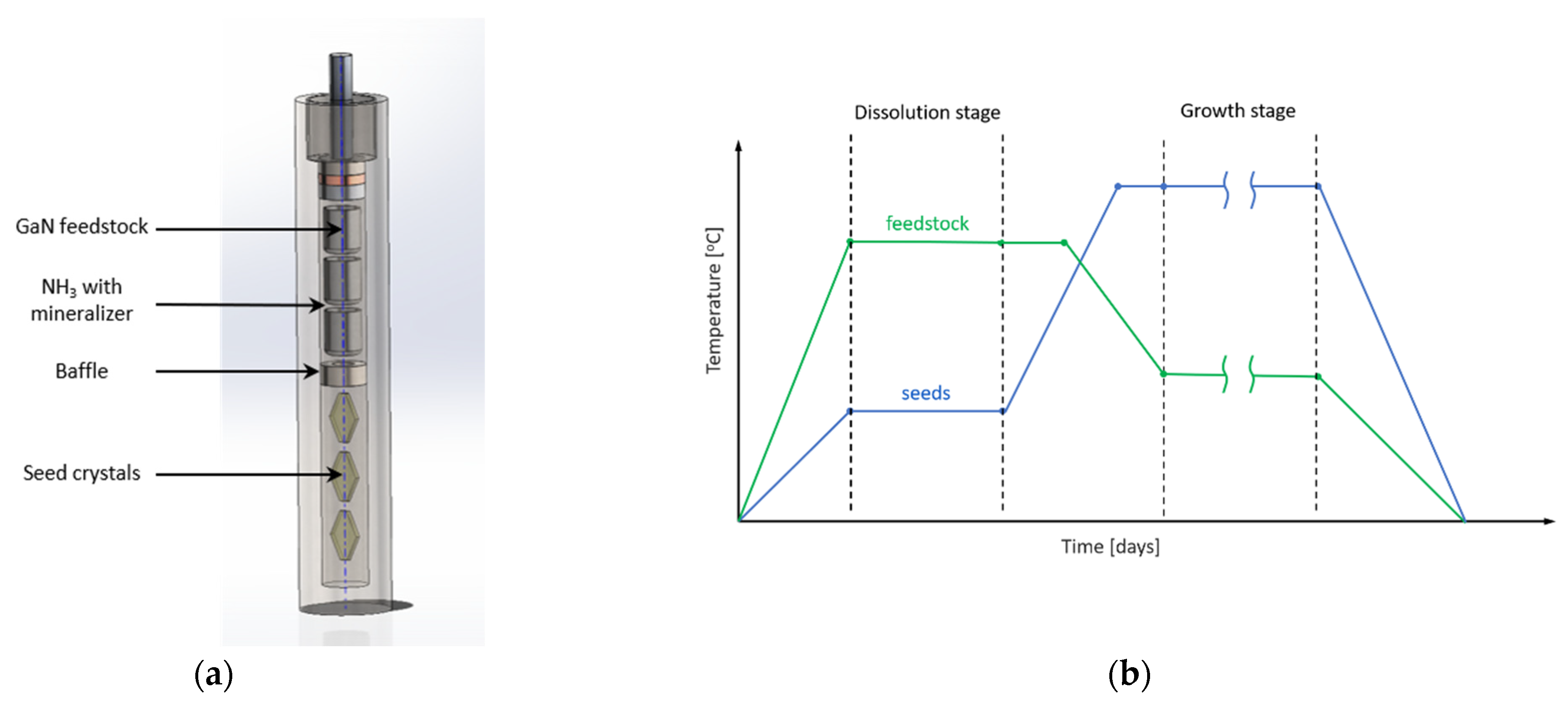
An ammonothermal crystallization process of GaN is conducted in a nickel-based alloy autoclave (reactor) of its own design and construction in a temperature range of 400–600 °C and NH
3 pressure of 0.3–0.4 GPa. A scheme of an ammonothermal autoclave with a typical interior configuration is presented in
Figure 1a. Crucibles with GaN feedstock are arranged one above the other in the upper part of the reactor. In the lower part, GaN seeds are placed on special holders. These two zones are separated by a baffle.
The seeds are always native ammonothermal GaN crystals. Their surfaces are not prepared in any special way. They can be as-grown, after slicing, after grinding, after mechanical polishing or epi-ready, i.e., after chemo-mechanical polishing (CMP). As already described [
15,
19], a typical ammonothermal crystallization run starts with a back-etching process. Then, all the seeds are kept at a lower temperature than the feedstock material. In time, the temperature profile changes, and the temperature of the growth zone with seed crystals is kept higher than that of the feedstock zone. The growth process starts, and GaN crystallizes on the etched surfaces of the native seeds. A scheme of the temperature–time relation of the two zones—with seeds and with feedstock—is presented in
Figure 1b.
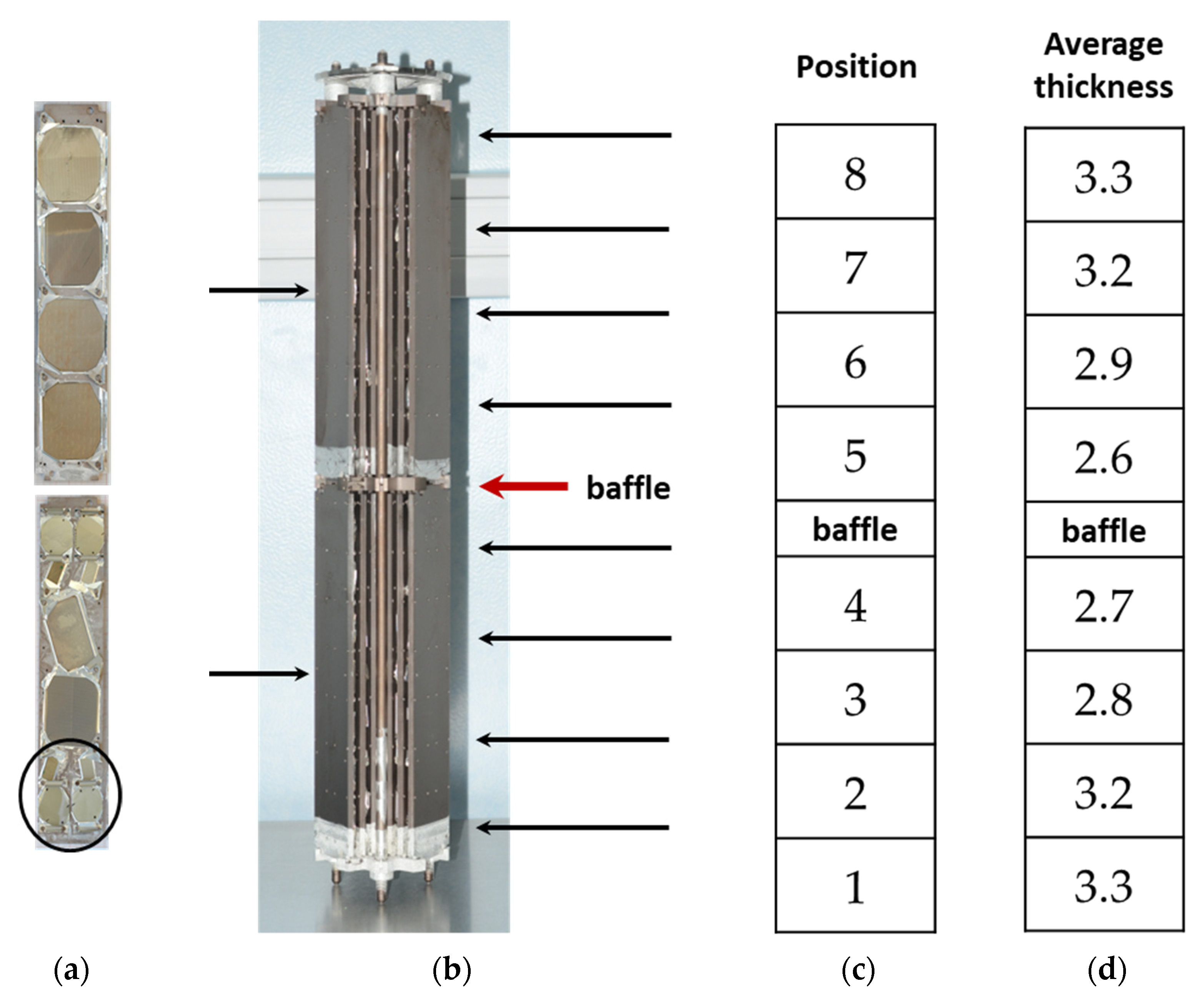
All the elements inside the autoclave are made of high-purity metals of well-known properties.
Figure 2a presents typical metal holders with GaN seeds used for an ammonothermal process. When the mounted seeds are of a diameter larger than 2 inches, they can be placed in four different positions. If the diameters of the seeds are smaller, they are placed close to each other, occupying an area for one 2-inch seed. Such a situation is marked by a black circle in
Figure 2a. Generally, growth is conducted in the <000-1> as well as the lateral <11-20> crystallographic directions. The seeds are wrapped in metal foil and attached to the metal holder.
Figure 2b shows a typical configuration of holders. Three holders can be placed at one level in the autoclave. There is space for 2 levels of holders. It allows for distinguishing eight positions (marked in
Figure 2c) of the seed crystals mounted on the holders. Approximately 3550 crystals grown in these positions were analyzed.
Figure 2d shows the average thicknesses of crystals grown on seeds placed in these 8 positions. It is clearly seen that these values vary for different seed positions. The crystals in the middle of the growth zone (Positions 3–6) are grown at a lower rate. It should also be noted that the highest percentage of SIPE presence (>50%) was recorded for Position 4.
2.2. Experimental
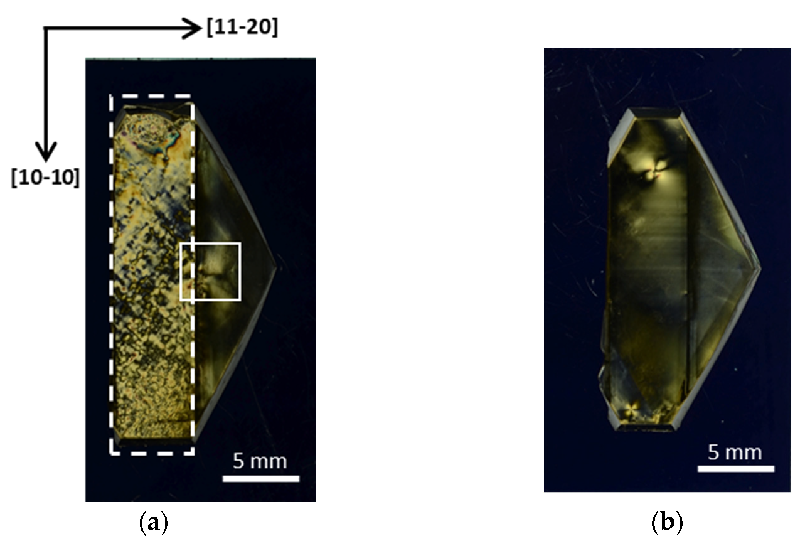
Figure 3 presents two rectangular seeds chosen for further growth process and examination. The (000-1) surface of each seed was prepared to an optically flat state by mechanical polishing with a 3 µm diamond grain gradation. No SIPE was detected in cross-polarized light in the two seeds. It means that no stress pattern was detected in them. Seed crystals No. 1 and No. 2 (see
Figure 3) were mounted at Position 4 (Pos. 4) and Position 1 (Pos. 1), respectively, in the ammonothermal autoclave. A typical ammonothermal process, as described above, was performed, and it lasted 76 days.
After the crystallization run, the two chosen seeds and crystals grown on them were analyzed in cross-polarized and UV light. A polariscope and an optical microscope (OM) Nikon Eclipse LV100ND with Nomarski contrast and UV illumination were applied. The (000-1) planes of the new-grown crystals, as well as cross-sections ((10-10)-planes) of the new-grown layer/seed systems, were examined in UV illumination. Attention was mostly paid to the interfaces. The samples were specially prepared for the UV illumination analyses (see
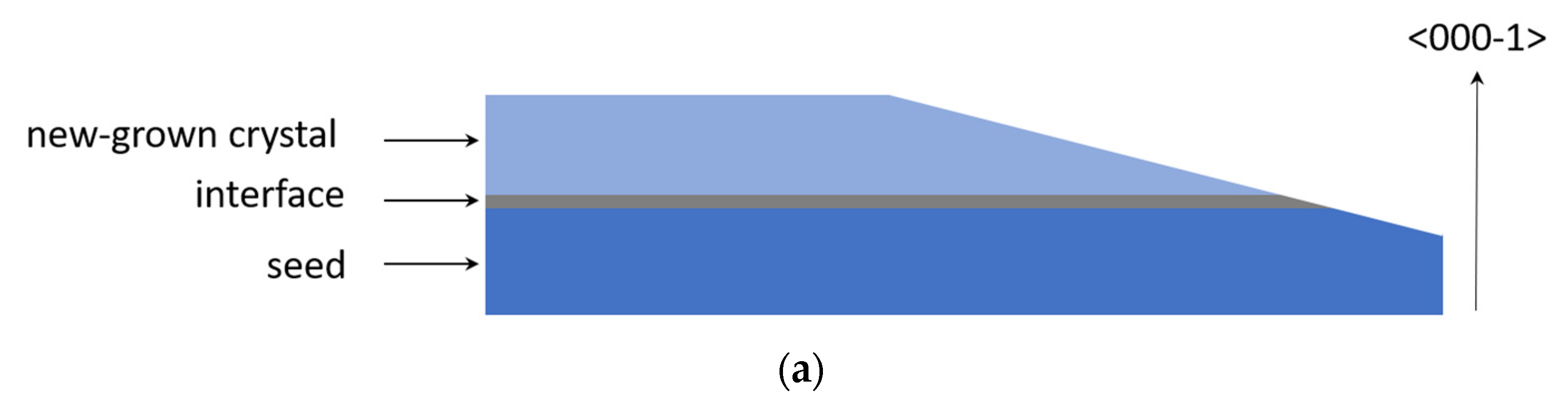
Figure 4a). Without removing the seeds, some parts of crystals grown in the [000-1] direction (a few millimeters square) were diced and then mechanically polished in such a way that the new-grown layer, the interface and the seed’s surface could be observed and examined at the same time.
Figure 4b presents the way of preparing samples for analyzing EPD by the defect selective etching (DSE) method (for details, see [
20]). The layers were sliced from the seeds above the interfaces. Next, the (0001) planes of the new-grown crystals as well as the seeds were prepared to an epi-ready state by chemo-mechanical polishing (CMP). These planes were then etched for 5 min in a KOH-NaOH solution at 450 °C. The samples were cleaned, and EPD was determined by counting etch pits at arbitrary chosen areas of a few square millimeters [
21,
22,
23].
3. Results
Figure 5 shows the two analyzed crystals after the ammonothermal run (images in cross-polarized light). The average growth rates were 37 µm/day and 44 µm/day for Crystals No. 1 and No. 2, respectively. SIPE was found in crystal No. 1 grown at Pos. 4. No SIPE was observed for crystal No. 2 grown at Pos. 1. It is clearly visible that in both cases the parts grown in the lateral [11-20] crystallographic direction were free of SIPE.
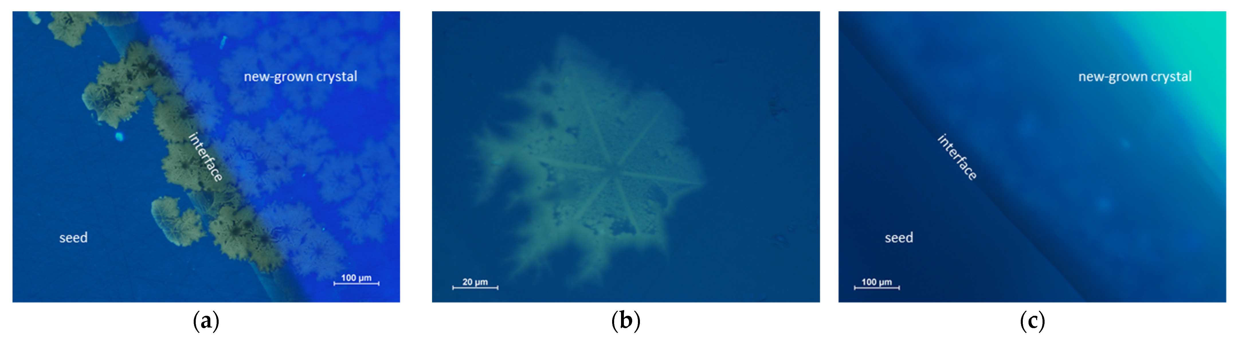
Figure 6 presents the surfaces (in UV illumination) of the two analyzed samples prepared in the way described above and presented in
Figure 4a. One can see the seed, the interface, and the new-grown crystal. For the sample where SIPE was detected (No. 1), some yellowish features are seen at the interface (see
Figure 6a).
Figure 6b demonstrates a magnification of one such feature at the interface (sample No. 1). A hexagonal symmetry of this yellowish figure is well visible. For crystal No. 2, without SIPE, the interface is flat with no visible features (see
Figure 6c).
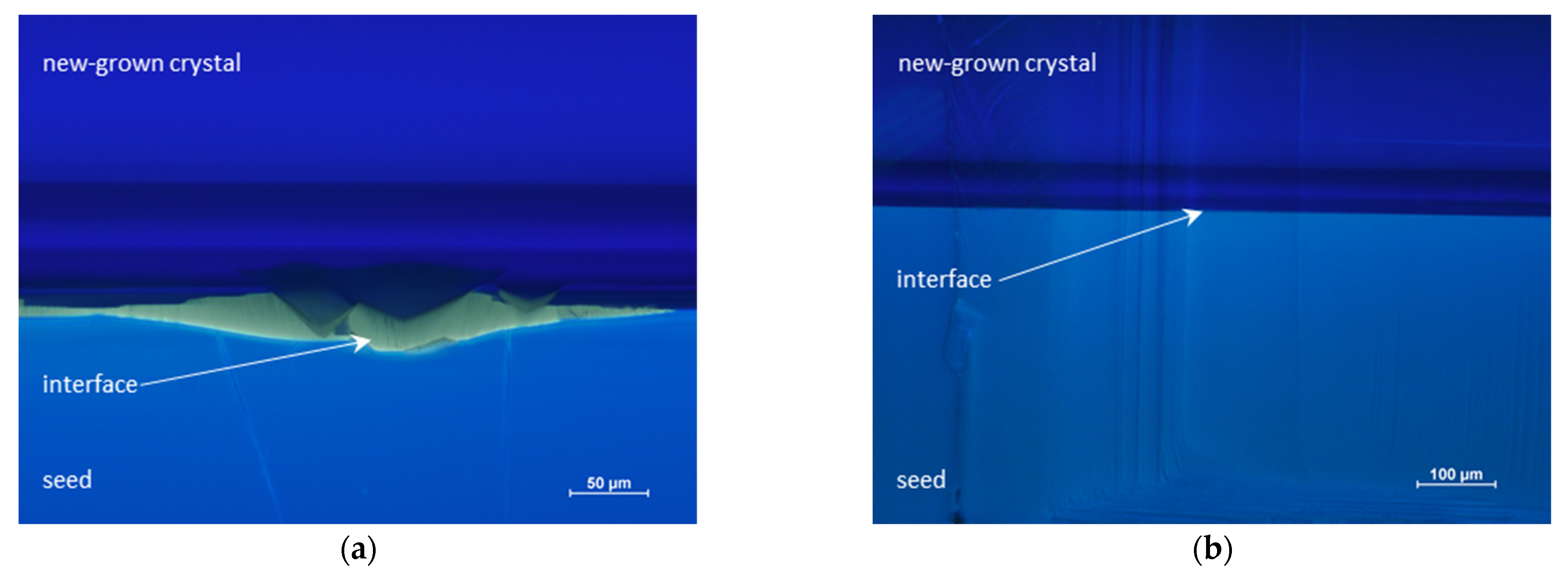
Figure 7a shows a cross-section, the (10-10) plane, of crystal No. 1 at UV illumination. It is easy to distinguish between the seed and the new-grown crystal. The interface between them is wavy. Additionally, yellow luminescence (YL) is present. In crystal No. 2, in turn, the interface looked flatter, without any traces of YL (see
Figure 7b).
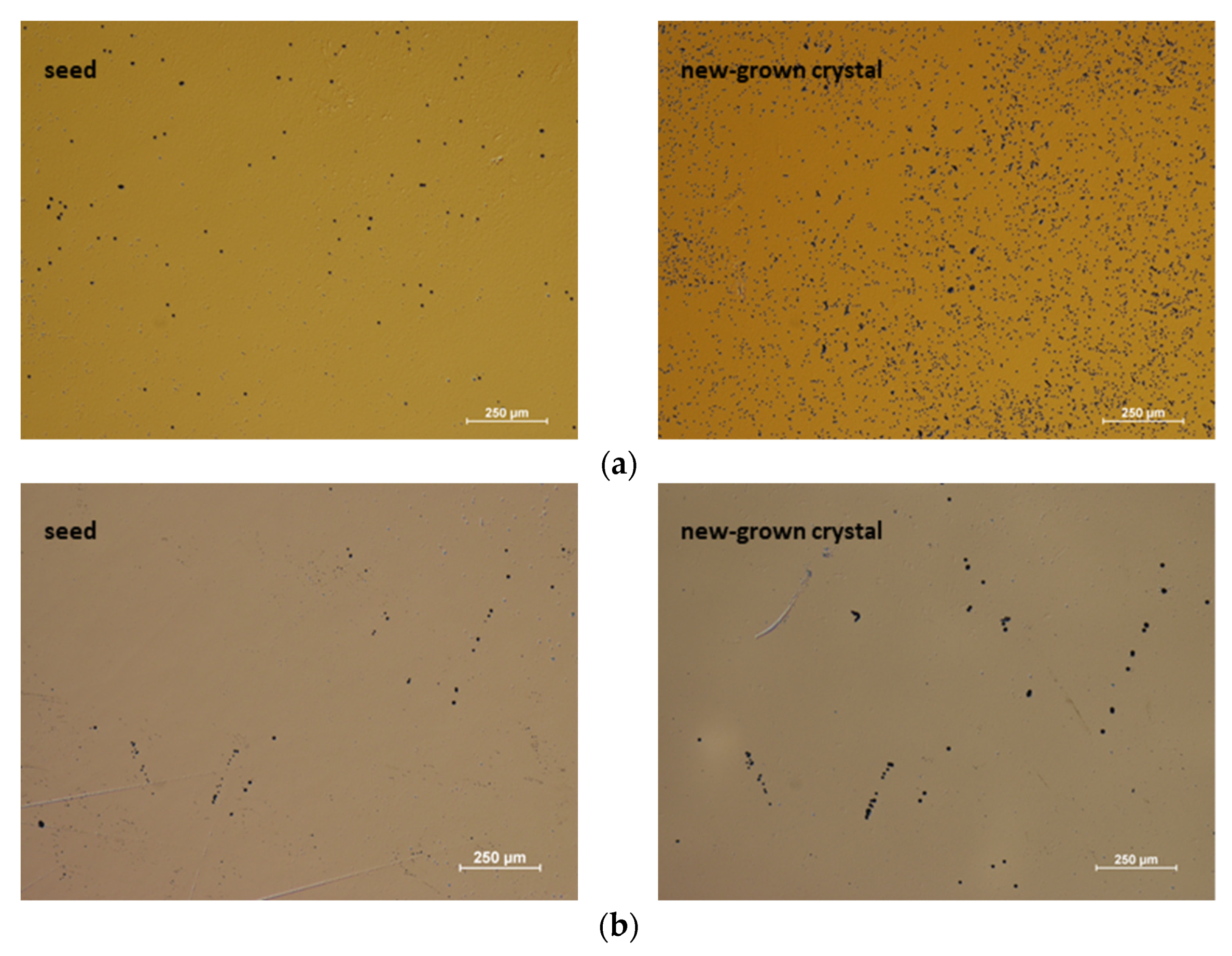
Figure 8 presents the seeds and the new-grown layers, prepared as presented in
Figure 4b, after DSE. As can be seen, there is a big difference in the EPD (one order of magnitude; from 10
4 cm
−2 to 3 × 10
5 cm
−2) between the seed and the new-grown layer for sample No. 1. For the second sample (No. 2), there is no difference in EPD in the seed and the new-grown crystal. For the same areas observed in the seed and the layer, even the positions of the pits look the same (see
Figure 8b).
4. Discussion
The occurrence of SIPE has become the main factor inhibiting the proper development of basic ammonothermal crystallization. SIPE is the reason why TDD in Am-GaN crystals can occasionally be higher than 5 × 10
4 cm
−2. Eliminating SIPE allows improving the structural quality of the crystals and thus the substrates. As mentioned in the Introduction, SIPE can be associated with the beginning of the crystallization process and non-uniform supersaturation in the crystal growth zone and individual growth fronts of the crystals. As reported in [
14,
15,
19], basic ammonothermal growth starts from the back-etching process. Then, the feedstock temperature is higher than the temperature of the crystal growth zone (see
Figure 1). The seed crystals are dissolved in the solution. If the surface of the seed is non-uniform (after slicing, grinding, lapping, or mechanical polishing), the etching process will also be non-uniform across the surface of the seed. First of all, subsurface damage (with an extremely high concentration of point defects [
24,
25,
26,
27]) that always exists in a not epi-ready surface will be revealed. The waviness of the interface will be formed due to several factors, e.g., selectivity of the etching process (surface with more damage will be etched faster) and spreading of deep pits formed on threading structural defects.
In order to exclude the seed’s surface preparation as the main reason for growth disturbance and SIPE formation, the (000-1) surfaces of the two seeds used for this research were in the same state: optically flat. Both seeds were free of SIPE. They were mounted at Positions 1 and 4 in the autoclave. As expected based on the statistics, the crystal grown at Pos. 4 demonstrated SIPE. The new crystal grown at Pos. 1 was SIPE-free. No doubt, the reason for SIPE formation was non-uniform supersaturation due to a non-uniform convective flow in the growth zone. In both cases, the growth started from an etched surface. Due to non-uniform convection, the etching was inhomogeneous, and, finally, the state of the (000-1) surface of the seeds at Positions 1 and 4 was different. At Pos. 4, a 3D growth mode appeared together with the formation of the yellowish features (see
Figure 6a). The non-uniformly etched surface tended to minimize its free energy. Therefore, low-energy semi-polar planes evolved. This was accompanied by different incorporation of dopants (YL visible at the interface), resulting in a change in the lattice parameters [
28,
29,
30]. The start of the growth process in the 3D mode caused the appearance of stress at the interface and then SIPE formation. This did not happen at Pos. 1, where the convection was more uniform, and the back-etching process and first stage of growth were quite homogeneous. In this case, the growth started in the two-dimensional (2D) growth mode with homogeneous incorporation of dopants. The stress was too low to be seen as SIPE. A similar phenomenon was also observed in crystal growth from the gas phase. Some impurities at the interface between the seed and the new-grown crystal can hinder or assist with later bulk growth [
31,
32].
The correctness of the presented model was confirmed by the DSE results and determination of EPD. When the interface between the seed and the new-grown crystal was flat but without significant incorporation of impurities (no YL; see
Figure 7b), the value of EPD was the same in the new-grown layer and in the seed (see
Figure 8b). This means that TDD did not increase in the new-grown crystal. When the interface was wavy with the presence of YL (significant incorporation of dopants), EPD increased in the layer. This indicates that TDD in the new-grown crystal also increased. The reason for this was the stress generated at the interface and then relaxation by the formation of new dislocations. The appearance of dislocations relaxes the crystal but never completely removes SIPE.
It should be mentioned that SIPE was not formed during the growth process in the lateral direction (see
Figure 5). Crystallization in the [11-20] direction has to be realized in a different way than in the [000-1] direction. Growth begins at the edge of the seed crystal. There is no surface underneath the newly crystallized material. This presents a chance to improve the structural quality of basic ammonothermal crystals in the near future. New seeds with low TDD should be obtained by the lateral growth process. In parallel, the convective flow should be studied and then controlled in order to be uniform in all positions in the growth zone. This should be conducted for both the back-etching and crystallization stages. The new seeds (without SIPE and with low TDD) could be used for the next generation crystallization processes in the [000-1] direction. Obviously, for completely excluding the 3D growth mode at the interface, the (000-1) surfaces of the seeds should have strictly defined misorientation (off-cut) and be prepared to an epi-ready state. Then, the back-etching conditions for the entire seed will be uniform. Thus, the surface will be homogenously etched (assuming that there are no cracks, inclusions, precipitates, or high TDD in the crystal). After such etching, the crystallization process should start from a 2D growth mode, by steps flown on the seed’s surface. In time, due to a lack of the steps source, the (000-1) plane will be recovered, and the 2D growth mode will change. Some hillocks will be formed.
5. Conclusions
The formation of SIPE, as well as its consequence (the emergence of new defects), in ammonothermally grown GaN crystals was determined in detail. Through a careful surface and interface analysis, it was demonstrated that a non-uniform back-etching process and the start of the crystallization process in a 3D growth mode can lead to stress formation in the growing crystals. This happens due to the non-uniform incorporation of dopants at the interface between the native seed and the new-grown GaN. Stress relaxation leads, in turn, to the formation of new defects in the growing crystal. The lack of stress in the Am-GaN crystal (a potential seed) means that either the crystal is stress-free (or the existing stress is very low) or there is an increased density of threading dislocations (the stress has already relaxed).
It is generally assumed that the convective flow of reagents and the seed’s surface preparation can influence the structural quality of the growing crystals and the formation of SIPE. In fact, the homogeneity of the growth process will depend on the uniformity of supersaturation. The latter, in turn, can be ensured by a homogenous and laminar convective flow of the reagents to the growth zone at proper and constant temperature–pressure conditions. A quantitative analysis of the convective transport at 3D approximation would allow us to find the best growth conditions for a uniform crystallization of GaN in each position in the crystal growth zone in an autoclave.
Author Contributions
K.G.—crystal growth experiments, characterization, preparing the manuscript; R.K.—crystal growth experiments, characterization; T.S.—crystal growth experiments, characterization; J.L.W.—DSE measurements; M.I.—review and editing; I.G.—supervision, review and editing; M.B.—supervision, review and editing. All authors have read and agreed to the published version of the manuscript.
Funding
This research was supported by the Polish National Science Center through Project No. 2021/41/N/ST5/03669 as well as by the Polish National Centre for Research and Development through project TECHMATSTRATEG-III/0003/2019-00. This research also received funding from the Department of the Navy, Office of Naval Research Global under ONRG award number N62909-21-1-2063 as well as the ECSEL Joint Undertaking (JU) under grant agreement No 101007310. The JU receives support from the European Union’s Horizon 2020 research and innovation program and Italy, Germany, France, Poland, the Czech Republic, and the Netherlands.
Institutional Review Board Statement
Not applicable.
Informed Consent Statement
Not applicable.
Data Availability Statement
The data presented in this study are available on request from the corresponding author.
Conflicts of Interest
The authors declare no conflict of interest.
References
- Amano, H.; Baines, Y.; Beam, E.; Borga, M.; Bouchet, T.; Chalker, P.R.; Charles, M.; Chen, K.J.; Chowdhury, N.; Chu, R.; et al. The 2018 GaN power electronics roadmap. J. Phys. D Appl. Phys. 2018, 51, 163001. [Google Scholar] [CrossRef]
- Kirste, R.; Sarkar, B.; Reddy, P.; Guo, Q.; Collazo, R.; Sitar, Z. Status of the growth and fabrication of AlGaN-based UV laser diodes for near and mid-UV wavelength. J. Mater. Res. 2021, 36, 4638–4664. [Google Scholar] [CrossRef]
- Ehrentraut, D.; Bockowski, M. Bulk Crystal Growth: Basic Techniques, and Growth Mechanisms and Dynamics. In Handbook of Crystal Growth, 2nd ed.; Rudolph, P., Ed.; Elsevier: Amsterdam, The Netherlands, 2015; pp. 577–619. [Google Scholar]
- Key, D.; Jordan, B.; Letts, E.; Hashimoto, T. Assessment of dislocation reduction on 100 mm diameter bulk GaN grown by the NEAT method. Jpn. J. Appl. Phys. 2022, 61, 030903. [Google Scholar] [CrossRef]
- Key, D.; Letts, E.; Tsou, C.-W.; Ji, M.-H.; Bakhtiary-Noodeh, M.; Detchprohm, T.; Shen, S.-C.; Dupuis, R.; Hashimoto, T. Structural and Electrical Characterization of 2” Ammonothermal Free-Standing GaN Wafers. Progress toward Pilot Production. Materials 2019, 12, 1925. [Google Scholar] [CrossRef] [Green Version]
- Hashimoto, T.; Letts, E.; Key, D.; Jordan, B. Two inch GaN substrates fabricated by the near equilibrium ammonothermal (NEAT) method. Jpn. J. Appl. Phys. 2019, 58, SC1005. [Google Scholar] [CrossRef]
- Iso, K.; Ikeda, H.; Mochizuki, T.; Mikawa, Y.; Izumisawa, S. High quality GaN crystal grown by hydride vapor-phase epitaxy on SCAATTM. Appl. Phys. Express 2020, 13, 085508. [Google Scholar] [CrossRef]
- Mikawa, Y.; Ishinabe, T.; Kagamitani, Y.; Mochizuki, T.; Ikeda, H.; Iso, K.; Takahashi, T.; Kubota, K.; Enatsu, Y.; Tsukada, Y.; et al. Recent progress of large size and low dislocation bulk GaN growth. In Gallium Nitride Materials and Devices XV, Proceedings of the SPIE OPTO 2020, San Francisco, CA, USA, 1–6 February 2020; SPIE: Bellingham, WA, USA, 2020; Volume 11280. [Google Scholar] [CrossRef]
- Iso, K.; Mikawa, Y.; Ikeda, H.; Hotta, K.; Mochizuki, T.; Izumisawa, S. Thermal annealing effects on SCAATTM substrate grown toward the c- and m-directions. Appl. Phys. Express 2019, 12, 125502. [Google Scholar] [CrossRef]
- Suihkonen, S.; Pimputkar, S.; Sintonen, S.; Tuomisto, F. Defects in Single Crystalline Ammonothermal Gallium Nitride. Adv. Electron. Mater. 2017, 3, 1600496. [Google Scholar] [CrossRef] [Green Version]
- Griffiths, S.; Pimputkar, S.; Speck, J.; Nakamura, S. On the solubility of gallium nitride in supercritical ammonia-sodium solutions. J. Cryst. Growth 2016, 456, 5–14. [Google Scholar] [CrossRef] [Green Version]
- Pimputhar, S. Single Crystals of Electronic Materials: Growth and Properties; Woodhead Publishing: Cambridge, MA, USA, 2019; pp. 351–399. [Google Scholar] [CrossRef]
- Meissner, E.; Niewa, R. (Eds.) Ammonothermal Synthesis and Crystal Growth of Nitrides; Springer Series in Materials Science; Springer International Publishing: Cham, Switzerland, 2021. [Google Scholar]
- Kucharski, R.; Sochacki, T.; Lucznik, B.; Amilusik, M.; Grabianska, K.; Iwinska, M.; Bockowski, M. Ammonothermal and HVPE Bulk Growth of GaN. In Wide Bandgap Semiconductors for Power Electronics: Materials, Devices, Applications; Wellmann, P., Ohtani, N., Rupp, R., Eds.; Wiley-VCH GmbH: Weinheim, Germany, 2021; Chapter 18. [Google Scholar]
- Kucharski, R.; Sochacki, T.; Lucznik, B.; Bockowski, M. Growth of bulk GaN crystals. J. Appl. Phys. 2020, 128, 050902. [Google Scholar] [CrossRef]
- Kirste, L.; Grabianska, K.; Kucharski, R.; Sochacki, T.; Lucznik, B.; Bockowski, M. Structural Analysis of Low Defect Ammonothermally Grown GaN Wafers by Borrmann Effect X-ray Topography. Materials 2021, 14, 5472. [Google Scholar] [CrossRef] [PubMed]
- Liu, Y.; Raghothamachar, B.; Peng, H.; Ailihumaer, T.; Dudley, M.; Collazo, R.; Tweedie, J.; Sitar, Z.; Shahedipour-Sandvik, F.S.; Jones, K.A.; et al. Synchrotron X-ray topography characterization of high quality ammonothermal-grown gallium nitride substrates. J. Cryst. Growth 2020, 551, 125903. [Google Scholar] [CrossRef]
- Available online: www.unipress.waw.pl (accessed on 1 March 2022).
- Grabianska, K.; Kucharski, R.; Puchalski, A.; Sochacki, T.; Bockowski, M. Recent progress in basic ammonothermal GaN crystal growth. J. Cryst. Growth 2020, 547, 125805. [Google Scholar] [CrossRef]
- Kamler, G.; Smalc-Koziorowska, J.; Nowak, G.; Grzegory, I.; Klepka, M.T. Influence of substrate planar defects on MOVPE GaN layer growth. Phys. Status Solidi A 2013, 210, 503–506. [Google Scholar] [CrossRef]
- Sochacki, T.; Amilusik, M.; Fijalkowski, M.; Iwinska, M.; Lucznik, B.; Weyher, J.L.; Kamler, G.; Kucharski, R.; Grzegory, I.; Bockowski, M. Examination of defects and the seed’s critical thickness in HVPE-GaN growth on ammonothermal GaN seed. Phys. Status Solidi B 2015, 252, 1172–1179. [Google Scholar] [CrossRef]
- Sochacki, T.; Bryan, Z.; Amilusik, M.; Collazo, R.; Lucznik, B.; Weyher, J.L.; Nowak, G.; Sadovyi, B.; Kamler, G.; Kucharski, R.; et al. Preparation of Free-Standing GaN Substrates from Thick GaN Layers Crystallized by Hydride Vapor Phase Epitaxy on Ammonothermally Grown GaN Seeds. Appl. Phys. Express 2013, 6, 075504. [Google Scholar] [CrossRef]
- Sochacki, T.; Sintonen, S.; Weyher, J.; Amilusik, M.; Sidor, A.; Bockowski, M. Synchrotron radiation X-ray topography and defect selective etching analysis of threading dislocations in halide vapor phase epitaxy GaN crystal grown on ammonothermal seed. Jpn. J. Appl. Phys. 2019, 58, SCCB19. [Google Scholar] [CrossRef]
- Reshchikov, M.A.; Vorobiov, M.; Grabianska, K.; Zajac, M.; Iwinska, M.; Bockowski, M. Defect-related photoluminescence from ammono GaN. J. Appl. Phys. 2021, 129, 095703. [Google Scholar] [CrossRef]
- Reshchikov, M.A.; Demchenko, D.O.; Ye, D.; Andrieiev, O.; Vorobiov, M.; Grabianska, K.; Zajac, M.; Nita, P.; Iwinska, M.; Bockowski, M.; et al. The effect of annealing on photoluminescence from defects in ammonothermal GaN. J. Appl. Phys. 2022, 131, 035704. [Google Scholar] [CrossRef]
- Tuomisto, F.; Mäki, J.-M.; Zając, M. Vacancy defects in bulk ammonothermal GaN crystals. J. Cryst. Growth 2010, 312, 2620–2623. [Google Scholar] [CrossRef]
- Tuomisto, F.; Kuittinen, T.; Zając, M.; Doradziński, R.; Wasik, D. Vacancy-hydrogen complexes in ammonothermal GaN. J. Cryst. Growth 2014, 403, 114–118. [Google Scholar] [CrossRef]
- Amilusik, M.; Sochacki, T.; Fijalkowski, M.; Lucznik, B.; Iwinska, M.; Sidor, A.; Teisseyre, H.; Domagała, J.; Grzegory, I.; Bockowski, M. Homoepitaxial growth by halide vapor phase epitaxy of semi-polar GaN on ammonothermal seeds. Jpn. J. Appl. Phys. 2019, 58, SC1030. [Google Scholar] [CrossRef]
- Amilusik, M.; Wlodarczyk, D.; Suchocki, A.; Bockowski, M. Micro-Raman studies of strain in bulk GaN crystals grown by hydride vapor phase epitaxy on ammonothermal GaN seeds. Jpn. J. Appl. Phys. 2019, 58, SCCB32. [Google Scholar] [CrossRef]
- Zajac, M.; Kucharski, R.; Grabianska, K.; Gwardys-Bak, A.; Puchalski, A.; Wasik, D.; Litwin-Staszewska, E.; Piotrzkowski, R.; Domagala, J.Z.; Bockowski, M. Basic ammonothermal growth of Gallium Nitride—State of the art, challenges, perspectives. Prog. Cryst. Growth Charact. Mater. 2018, 64, 63–74. [Google Scholar] [CrossRef]
- Kakanakova-Georgieva, A.; Gueorguiev, G.K.; Yakimova, R.; Janzén, E. Effect of impurity incorporation on crystallization in AlN sublimation epitaxy. J. App. Phys. 2004, 96, 5293. [Google Scholar] [CrossRef]
- Dos Santos, R.B.; Rivelino, R.; de Brito Mota, F.; Gueorguiev, G.K.; Kakanakova-Georgieva, A. Dopant species with Al–Si and N–Si bonding in the MOCVD of AlN implementing trimethylaluminum, ammonia and silane. J. Phys. D Appl. Phys. 2015, 48, 295104. [Google Scholar] [CrossRef]
| Publisher’s Note: MDPI stays neutral with regard to jurisdictional claims in published maps and institutional affiliations. |
© 2022 by the authors. Licensee MDPI, Basel, Switzerland. This article is an open access article distributed under the terms and conditions of the Creative Commons Attribution (CC BY) license (https://creativecommons.org/licenses/by/4.0/).


 ,
, 


