Article

First-Principles Assessment of the Structure and Stability of 15 Intrinsic Point Defects in Zinc-Blende Indium Arsenide

1
Nuclear Engineering and Radiological Sciences, University of Michigan, Ann Arbor, MI 48109, USA
2
Space Vehicles Directorate, Air Force Research Laboratory, Kirtland AFB, Albuquerque, NM 87117, USA
3
Materials and Manufacturing Directorate, Air Force Research Laboratory, Wright Patterson AFB, OH 45433, USA
*
Authors to whom correspondence should be addressed.
Submission received: 4 December 2018 / Revised: 14 January 2019 / Accepted: 15 January 2019 / Published: 17 January 2019
(This article belongs to the Special Issue First-Principles Prediction of Structures and Properties in Crystals)

Abstract

:
Point defects are inevitable, at least due to thermodynamics, and essential for engineering semiconductors. Herein, we investigate the formation and electronic structures of fifteen different kinds of intrinsic point defects of zinc blende indium arsenide (zb-InAs ) using first-principles calculations. For As-rich environment, substitutional point defects are the primary intrinsic point defects in zb-InAs until the n-type doping region with Fermi level above 0.32 eV is reached, where the dominant intrinsic point defects are changed to In vacancies. For In-rich environment, In tetrahedral interstitial has the lowest formation energy till n-type doped region with Fermi level 0.24 eV where substitutional point defects In A s take over. The dumbbell interstitials prefer < 110 > configurations. For tetrahedral interstitials, In atoms prefer 4-As tetrahedral site for both As-rich and In-rich environments until the Fermi level goes above 0.26 eV in n-type doped region, where In atoms acquire the same formation energy at both tetrahedral sites and the same charge state. This implies a fast diffusion along the t T t path among the tetrahedral sites for In atoms. The In vacancies V I n decrease quickly and monotonically with increasing Fermi level and has a q = 3 e charge state at the same time. The most popular vacancy-type defect is V I n in an As-rich environment, but switches to V A s in an In-rich environment at light p-doped region when Fermi level below 0.2 eV. This study sheds light on the relative stabilities of these intrinsic point defects, their concentrations and possible diffusions, which is expected useful in defect-engineering zb-InAs based semiconductors, as well as the material design for radiation-tolerant electronics.

1. Introduction

The III-V zinc-blende semiconductors are among the most important semiconductors, and have recently received much attention since they have potential to be employed as base materials for light-emitting diodes, infrared photodetectors, and spintronic devices, e.g., quantum-dot and quantum-well applications [1,2,3]. The materials have been the subject of interest in a large variety of experimental and theoretical investigations [4,5,6]. The III-V semiconductors are strong candidates to be incorporated into high-performance opto-electronics due to their direct band gap and high electron mobility [7,8]. In the family of III-V materials, InAs stands out because of its very high electron mobility which can be as much as three times higher than those in InGaAs and GaAs [7,9]. Meanwhile, it also acquires a small direct band gap of 0.35 eV at room temperature and a low carrier effective masses as well [10]. Together, these properties make InAs a promising candidate for incorporation into next-generation nano-electronics [7]. Additionally, InAs has already been made successfully into nanowires [11,12,13] and demonstrated to integrate well into novel field-effect transistor (FET) device geometries [14,15,16,17].
Due to its important applications in electronics, extensive efforts have been put in studying the electronic properties and performance of nanowire-based devices [18,19,20] and quantum dots [21]. It is also desirable to understand the instabilities in these materials and devices under severe conditions including radiation damage and their survivability under single event upset [22,23]. One of the fundamental questions is the formation energy of point defects, which is essential to understand the creation of defects from an energetics aspect. Moreover, thermodynamic arguments suggest that the intrinsic or native defects will be inevitably present within a crystal at finite temperatures.
Under ambient conditions, InAs crystallizes into a cubic zinc-blende ( z b ) geometry with space group F 4 ¯ 3 m (T d 2 ) [24]. The atomic structure of pristine zb-InAs in a conventional eight-atom unit cell is depicted in Figure 1a, and we will limit our study to this type of crystalline structure. In this computational study, we primarily focus on the formation energy of various point defects, providing insights in understanding defect energetics within the bulk InAs crystal. For enhancing accuracy, our calculations are performed at the Ab initio level using density-functional theory (DFT). Generally, DFT describes reasonably well the structural properties, such as lattice constants and bulk moduli [25]. For a more accurate description of defect structures, we have carried out the investigation with enlarged simulation cells (216 lattice sites systems) to ensure that the accuracy is within 0.02 eV/cell. A 3 × 3 × 3 supercell with 108 In and 108 As atoms and referenced for defect calculations is illustrated in Figure 1b. Our study aims to provide an extensive and accurate study of the intrinsic point defect formation which is missed in the literature, e.g., a very recent computational study [26], but is highly desirable.
The remainder of this paper is organized as follows. Section 2 presents the computational method, including the formula for defect formation energy and the finite-size corrections, as well as the details of DFT calculations. The results and analysis are presented in Section 3, discussing the Fermi-level dependence of the formation energies of fifteen intrinsic defects in five groups under different chemical environments and in various charge states. The conclusions are provided in Section 4.

2. Methods

2.1. Defect Formation Energy

To reduce the artificial self-image interactions imposed by periodic-boundary conditions, defects are generally modeled in an enlarged super cell. The selection of the super-cell size is a compromise between the accuracy and the computing demands. In general, the formation energy for a defect with charges in a semiconductor or an insulator has contributions from both ions and electrons. In a super-cell formalism, for a defect or impurity X in a charge state q, its formation energy E f ( X q ) is computed by
E f ( X q , E F ) = E t o t ( X q ) E b u l k t o t ( q = 0 ) i Δ n i μ i + q ( E V B M + E F ) + E c o r r ,
where E t o t ( X q ) is the total energy of the super-cell containing the defect X in the charge state q, E b u l k t o t ( q = 0 ) denotes the total energy of the pristine bulk supercell which is neutral and free of any defects, Δ n i represents the number of atoms of species i added to ( Δ n i > 0 ) or removed from ( Δ n i < 0 ) the supercell as a result of the defect formation, and μ i = μ i b u l k + Δ μ i corresponds to the chemical potential of element species i. When an atom is added to the system, the associated electrons are also added to the system and contribute to the formation energy. Such a contribution is described by the chemical potential of electrons, known as the Fermi level E F at zero temperature. Here, E F of a semiconductor is treated as an independent variable that can take any value within the bandgap. It is worth noting that E F is measured with respect to E V B M , the energy of valence band maximum (VBM) of the bulk material.
Since the exact value of the chemical potential μ i in Eqaution (1) cannot be determined, it is treated as a parameter for the formation energy calculations. As such, the defect formation energies are given in the limiting conditions of As-rich and In-rich growth regimes. In the As-rich regime, the chemical potential of As atoms is assumed to be the value in bulk As, whereas in the In-rich (As-poor) regime, it corresponds to the chemical-potential difference between InAs and bulk In (and vice versa for the chemical potential of In). For an in-depth discussion of formation-energy calculations, the reader is referred to the following papers [27,28,29,30].
The correction term E c o r r in Equation (1) is used to remove the errors introduced by finite size (L) effects and periodic-boundary conditions, such as spurious overlaps of neighboring defect wave functions and, in case of charged defects, Coulomb interactions between image charges. There is still extensive debate on the performance and applicability of different schemes of corrections [31,32,33], e.g., Makov and Payne (MP) scheme [34], alignment-only scheme [35], Freysoldt, Neugebauer and Van de Walle (FNV) scheme [36], Lany and Zunger (LZ) scheme [37]. The mutual relation between various schemes and defining the conditions for their applications are discussed by Komsa et al. [38]. The classical MP scheme is adopted in this paper and gives the correction terms as
E c o r r ( q , L ) = E m o n o c o r r + E q u a d c o r r = α q 2 ϵ L + A 3 L 3 .
Here, the first term is the monopole Madelung term [32], while the second term is the third-order quadrupole electrostatic correction. In addition, α is the Madelung constant of the crystal, q is the charge of a defect state, embedded in a uniform compensating background charge, with the unit of e (the positive electron charge). ϵ is the static dielectric constant. The third-order parameter A 3 is taken as a fitting parameter.
Several early studies indicated that the quadrupole correction does not always improve results, leaving its utility somewhat in question [39,40]. Therefore, in this paper we only consider the leading term of the monopole Madelung correction. The Madelung constant α is 1.638 for zinc blende cubic lattice of point charges, and 2.8373 for simple cubic lattice of point charges. Within the approximation of a single charge monopole, we adopt α = 2.8373 for the cubic system. ϵ = 15.15 is chosen for the static dielectric constant of InAs.

2.2. Details of Density Functional Theory Calculations

The conventional unit cell contains eight atoms (four In and four As atoms). We used a 3 × 3 × 3 supercell containing 216 regular lattice sites, which consists of 108 In and 108 As atoms before including defects. The total energies of the system and forces on each atom are characterized via first-principles calculations within the framework of DFT. All DFT calculations are carried out with the Vienna Ab-initio Simulation Package (VASP) [41,42] which is based on the Kohn-Sham density-functional theory (KS-DFT) [43,44] with generalized gradient approximation for the exchange-correlation functionals [45] as parameterized by Perdew, Burke and Ernzerhof (PBE) and revised for solids (PBEsol) [46]. The electrons explicitly included in the calculations are the 4 d 10 5 s 2 5 p 1 electrons (13 electrons) and the 4 s 2 4 p 3 electrons (5 electrons) for each of In and As atom, respectively. The core electrons are replaced by the projector augmented wave (PAW) and pseudo-potential approach [47,48]. A plane-wave cutoff of 400 eV is used in the geometry relaxation to reduce Pulay stress. For all other calculations, we employ a plane-wave cutoff of 240 eV with accurate and dense k-mesh, where the irreducible Brillouin Zone is sampled with a Gamma-centered 3 × 3 × 3 k-mesh. Moreover, the calculations were performed at zero temperature. The criterion for stopping the relaxation of the electronic degrees of freedom is set by requiring the total energy change to be smaller than 10 5 eV. The optimized atomic geometry is achieved through minimizing Hellmann-Feynman forces acting on each atom until the maximum forces on ions become smaller than 0.01 eV/Å.
After the geometry optimization of a perfect crystal, we introduce defects by either removal of an appropriate atom to create a vacancy, or addition of an extra atom to create an interstitial in a pre-specified position (tetrahedral or dumbbell). The resulting structures were allowed to relax energetically, permitting atoms to move in all three dimensions. Here, all geometry optimizations were performed using the classical conjugate gradient algorithm.
It is well known that GGA level exchange correlation functions severely underestimate the band gaps of semiconductors, although the the total energy of the system could be obtained with fairly and satisfactorily accurate [49]. More accurate bandgap prediction require higher level exchange correlation functionals including GW and HSE methods [25]. However, because the defective systems are in general contain hundreds of atoms, for example, about 216 atoms in this study, it is unfeasible to carry out higher levels (GW, or HSE for example) calculations. Therefore, here we used the experimental (0.417 eV) of the band gap throughout this study, as previous efforts [31,49,50].

3. Results and Analysis

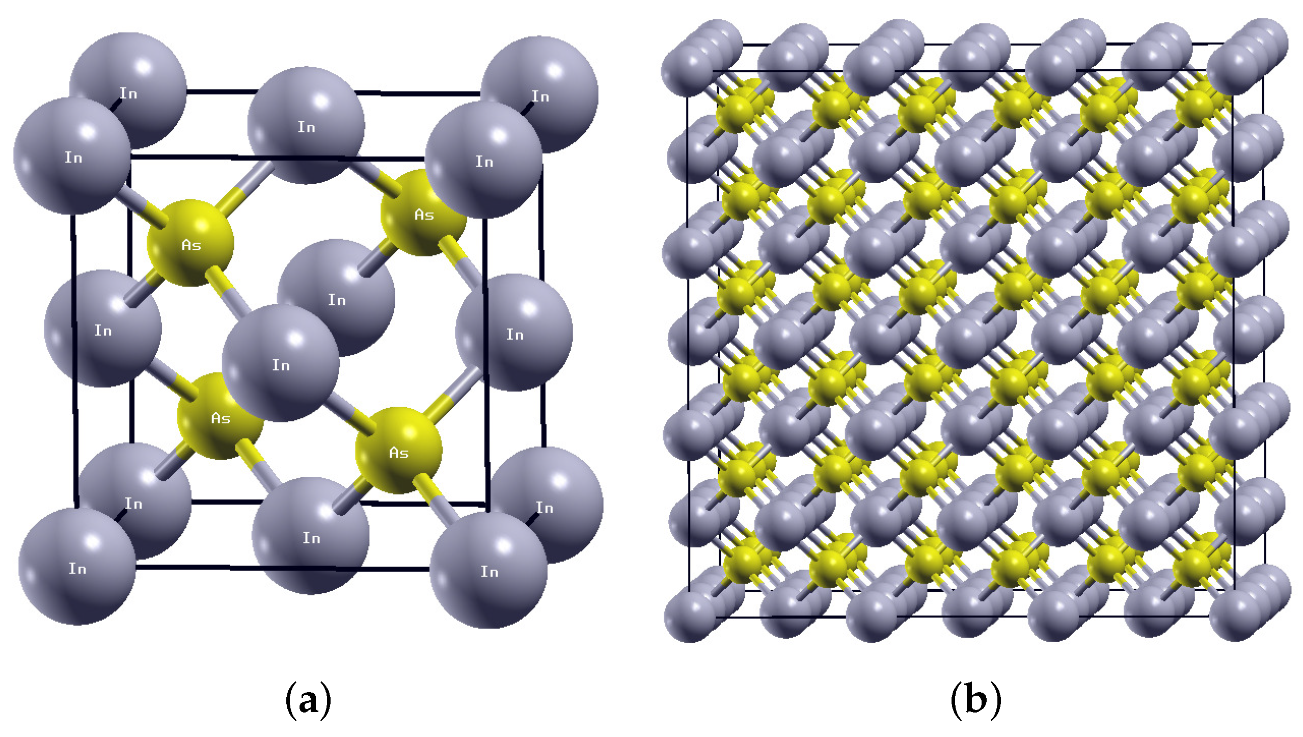
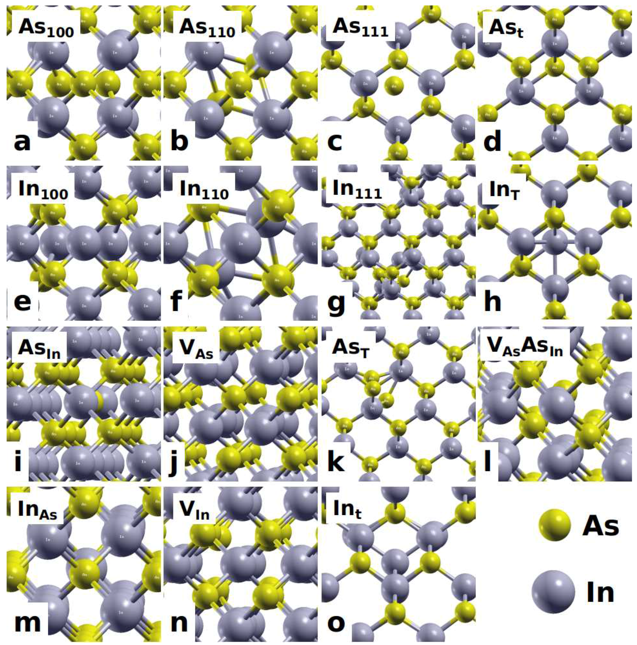
3.1. Atomic Structures of Intrinsic Defects

Under the ambient condition, InAs, one of the most important III-V semiconductors, has a cubic 3C zinc-blende crystalline configuration, We first optimized the geometry of the pristine zb-InAs with lattice parameters measured between 6.0584 Å and 6.060 Å [51]. Our result with the lattice parameter of 6.058 Å from GGA-PBEsol agrees well with previous GGA-PBE results of 6.059 Å [20], PBE-PW91 results of 6.061 Å [52], and experiment of 6.0588 Å reported by Thompson, Rowe, and Bubenstein in 1969 [53].
We then generated fifteen different defect configurations for intrinsic point defects in zb-InAs, as depicted in Figure 2. Each defect configuration sits around the center of a 3 × 3 × 3 supercell with 216 lattice sites, which ensures that the interactions between images become negligible. All these defect configurations are fully relaxed so that the maximum amplitude of the forces on every atom is less than 0.02 eV/Å. The final relaxed atomic structures of these fifteen configurations in neutral states (charge q = 0 ) are displayed in Figure 2. For denotation of these point defects, we take the form of the element or vacancy (V) with a subscript of the site. For example, As 110 means a configuration with an As atom on the < 110 > dumbbell position, and In A s means a configuration with an In atom substituting for an As atom on the site.
The defects in Figure 2 are divided into five groups. Group-1 is the dumbbell interstitial-type point defects. The dumbbell configuration is characterized by two atoms of the same species sharing one lattice site. There are three typical orientations: < 100 > , < 110 > , and < 111 > . Therefore, there exist totally six dumbbell configurations: (a) As 100 , (b) As 110 , (c) As 111 , and (e) In 100 , (f) In 110 , (g) In 111 as seen in Figure 2. Group-2 is the tetrahedral interstitial-type point defects. There are two kinds of tetrahedral sites in a zb-InAs lattice: one is formed by four In atoms denoted as t site, and the other is formed by four As atoms denoted as T site. Both In and As atoms could take either atom site, resulting in four tetrahedral interstitial-type point defects: (d) As t , (h) In T , (k) As T , and (o) In t as presented in Figure 2. Group-3 is the substitutional point defects, where a pristine As site is replaced by an In atom, or vise versa. The two intrinsic substitutional point defects in zb-InAs are (i) As I n and (m) In A s as shown in Figure 2. Group-4 is the vacancy-type point defects. There are two types of intrinsic vacancy-type point defects in zb-InAs: (j) V A s and (n) V I n , as displayed in Figure 2. The last Group-5 is a point-defect complex such as V A s As I n , which is formed by an As vacancy V A s combined with a substitutional As atom on the nearest-neighbor In site (As I n ), as demonstrated by Figure 2o. This defect is interesting because an In vacancy V I n could attract a nearby As atom to fill it up, resulting in the V A s As I n complex. It is worth pointing out that the relaxed atomic structures of the dumbbell interstitial-type defect of In 111 and tetrahedral interstitial-type defect of As T are also point-defect complexes, indicating they are highly unstable. Next, we investigate the formation energies of all these different types of defects.

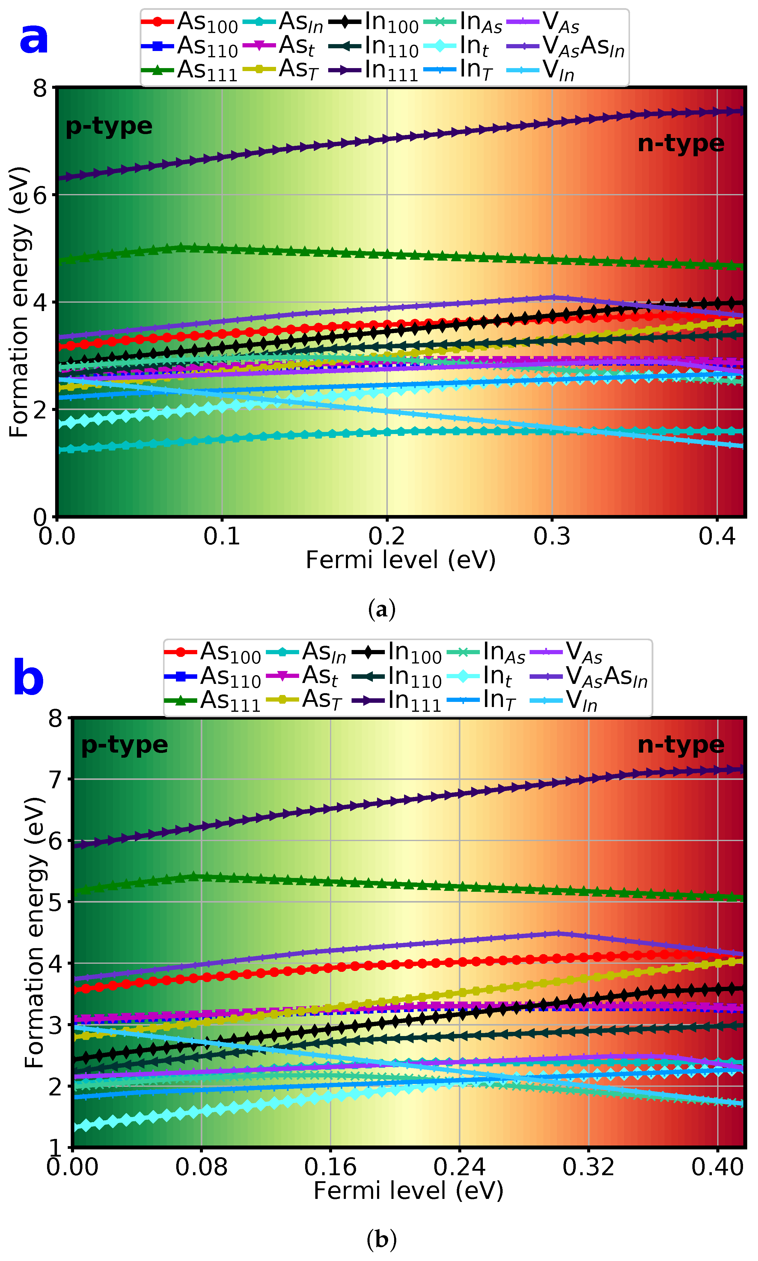
3.2. Defect Formation Energies

The formation energies of defects are computed according to Equation (1) for different charge states from q = 4 to q = 4 . In order to estimate the uncertainties caused by the finite size of supercells as well as the spurious image interactions, we therefore evaluate the corrections, as detailed in Section 2. As a result, we find the deviations up to 0.01 eV for defects with a charge of q = ± 4 . We regard these values as unavoidable uncertainties which nevertheless do not significantly alter the main conclusions.
It is clear from the formula in Equation (1) that the formation energies of intrinsic defects will depend on the choice of chemical potentials, i.e., the choice of reservoir with which equilibrium is achieved. The chemical potentials are constrained by equilibrium conditions, which varies from case to case, location to location, time to time. Here we only consider two extreme conditions: (1) As-rich and (2) In-rich. Our results of the chemical potentials are computed as μ A s b u l k = 3.014 eV, μ I n b u l k = 2.389 eV, and μ I n A s b u l k = 6.574 eV.
Another factor we need to consider is the Fermi level E F , which is required for counting the formation energies from the electrons’ contribution. However, the exact value of E F is very sensitive to local environments including doping concentrations. Consequently, we have expressed the defect formation energy as a function of E F which varies in the whole range of the electronic band gap. The experimental value of the bandgap is 0.417 [51]. We adopted this value as the range for E F in our study. In fact, the formation energy depends linearly on the Fermi level, as manifested in Equation (1). The band-gap predicted from PBE solid is 0.142 eV, which is severely underestimated from the experimental value of 0.417 eV, because the artificial self-interaction of electrons are not excluded [54]. Here we have applied the “extended gap scheme” to map the calculated transfer levels onto the experimental band gap [39]. The regime near the edge of the valence bands or VBM is the p-type doped where E F is small. The regime near the edge of the conduction bands or CBM is the n-type doped and E F is large and comparable to the band gap. The two two different regimes are dislayed in the figures of the formation energies to mark the doping stage through out this study.
The formation energies of fifteen defect configurations in the dilute limit are computed using the supercell method as aforementioned. It is worth mentioning that although the point defects are generated in a non-equilibrium process, the relative formation energies of different configurations can shed light on preferential locations and determine the accessible ground-state charge states, as well as charge-state transition levels [54]. The formation energies as functions of E F in the As-rich and In-rich environments for all these intrinsic defects in zb-InAs with all possible charge states from 4 to + 4 are displayed in the upper and lower panels of Figure 3, respectively. Our results show the distinctive trend and significant variations of the formation energies under various charge states as functions of E F for each point defect in both As-rich and In-rich environments. All calculated formation energies lie between 1.0 eV and 9.0 eV. The general trend is that the formation energy decreases for negative charge state ( q < 0 ) but increases for positive charge state ( q > 0 ) with increasing E F . The slope of the formation energy as a function of E F is positively correlated with the charge state. For q = + 4 e , the amount of the increment in formation energy is more than 1.5 eV as E F changes from VBM (0 eV) to CBM (0.417 eV).
The defect formation energy is the minimum energy for the generation of a defect. It is more practical to analyze the minimum formation energies among all the possible charge states given the fact that electrons have much higher mobilities (over three order of magnitude) than atoms. Therefore, we define the lowest formation energy of a defect as the minimum formation energy with respect to all possible charge states with 4 q 4 . We would focus on the discussion of the lowest formation energies of these defects in the following subsections. For simplicity, the formation energy refers to the lowest formation energy among various charge states hereafter until specified. Such lowest formation energies as functions of E F for each of fifteen defective configurations are presented in Figures S1 and S2 in the Supplementary Information for As-rich and In-rich environments, respectively. Here, we only discuss the lowest formation energies for five selected defect groups in the following subsections.

3.3. Formation Energy of Dumbbell Interstitials

As one atom squeezes itself into a lattice site taken by the same species in the pristine configuration, a dumbbell interstitial-type point defect will be formed. We explicitly examined six dumbbell interstitials of As 100 , As 110 , As 111 , In 100 , In 110 , In 111 depicted in Figure 2. The configuration of In 111 after relaxation becomes much different from the original < 111 > dumbbell structure (not shown here but similar to Figure 2c for As 111 with species switched). This result indicates that In 111 is unstable and will relax to a complex simultaneously. The formation energies of these six dumbbell interstitials as function of E F in As-rich and In-rich chemical environments are shown in the left and right panel, respectively, of Figure 4. In 111 and As 111 are found to have the two highest formation energies for both cases, indicating that the < 111 > dumbbell configurations are unfavorable for either environment and both In and As atoms.
For an As-rich environment, the As 110 has over all the lowest energy among the six dumbbell interstitials, followed by In 110 and In 100 . It is worth noting that in the very light p-doped region E F < 0.02 eV, In 110 has slightly (< 0.03 eV) lower formation energy than that of As 110 , which should be indistinguishable within this DFT study. For an In-rich environment, the configurations with the lowest three formation energies are In 110 , In 100 , and As 110 , similar to the As-rich case with switched elements. Therefore, we can conclude that the dumbbell interstitials prefer < 110 > configurations in zb-InAs under various charge states, chemical environment, and Fermi levels.

3.4. Formation Energy of Tetrahedral Interstitials

The tetrahedral sites are among the most energetic favorable sites for interstitials in diamond and zinc-blende structures. The four intrinsic tetrahedral interstitials are studied explicitly for (1) As on 4-As formed tetrahedral site As t , (2) As on 4-In formed tetrahedral site As T , (3) In on 4-As formed tetrahedral site In t , (4) In on 4-In formed tetrahedral site In T . Their corresponding formation energies are displayed in Figure 5 as functions of E F for both As-rich and In-rich chemical environments. In the whole Fermi level, In t has the lowest formation energy for both chemical environments, followed by In T . When E F > 0.26 eV, In T has the same formation energy as In t structure. In the very light p-doped region of E F < 0.02 eV, In t prefers + 4 e charge states. With the increase of doping, In t prefers + 3 e charge state in the p-doped region but + 1 e in the n-type doped region. The As tetrahedral interstitials are much less common in all chemical environments because their formation energy are much larger than that of In tetrahedral interstitials. As T prefers + 3 e charge state, opposed to As t with + 1 e or neutral state, in both chemical environments. The energy difference between As and In tetrahedral interstitials is larger in In-rich environment then that in As-rich environment.
The most interesting feature of the formation energy of tetrahedra interstitials is that for both As-rich and In-rich environments, In atoms prefer the 4-As tetrahedral site until E F > 0.26 eV, where In atoms have the same formation energy at both tetrahedral sites with the same charge state. The identical formation energies and charge states suggest a fast diffusion for In atoms along the t T t T path among tetrahedral sites. Additionally, in an In-rich environment, the formation energies of In tetrahedral interstitials are very low, less than 2 eV. Furthermore, for the p-doping case, In t has a small formation energy of 1.3 eV and with the charge state of q = + 3 e . Here, the low defect formation energy implies that the concentration of the corresponding defects is high under thermal equilibrium. Therefore, in the In-rich environment, In atoms prefer a tetrahedral sites with fast diffusion along the t T t path. The quantities that describe the diffusion dynamics, including diffusion energy barrier and diffusion coefficients, deserve further study.
Finally, in In-rich environment, the formation energies of both As T and As t are much higher (about 2 eV) than those of In counterparts, implying that As tetrahedral interstitials are energetically unlikely to form. As a contrast, in the As-rich environment, all the formation energies of As and In interstitials become close to each other. As a result, As-type tetrahedral interstitials are preferred in this case with lower formation energies.

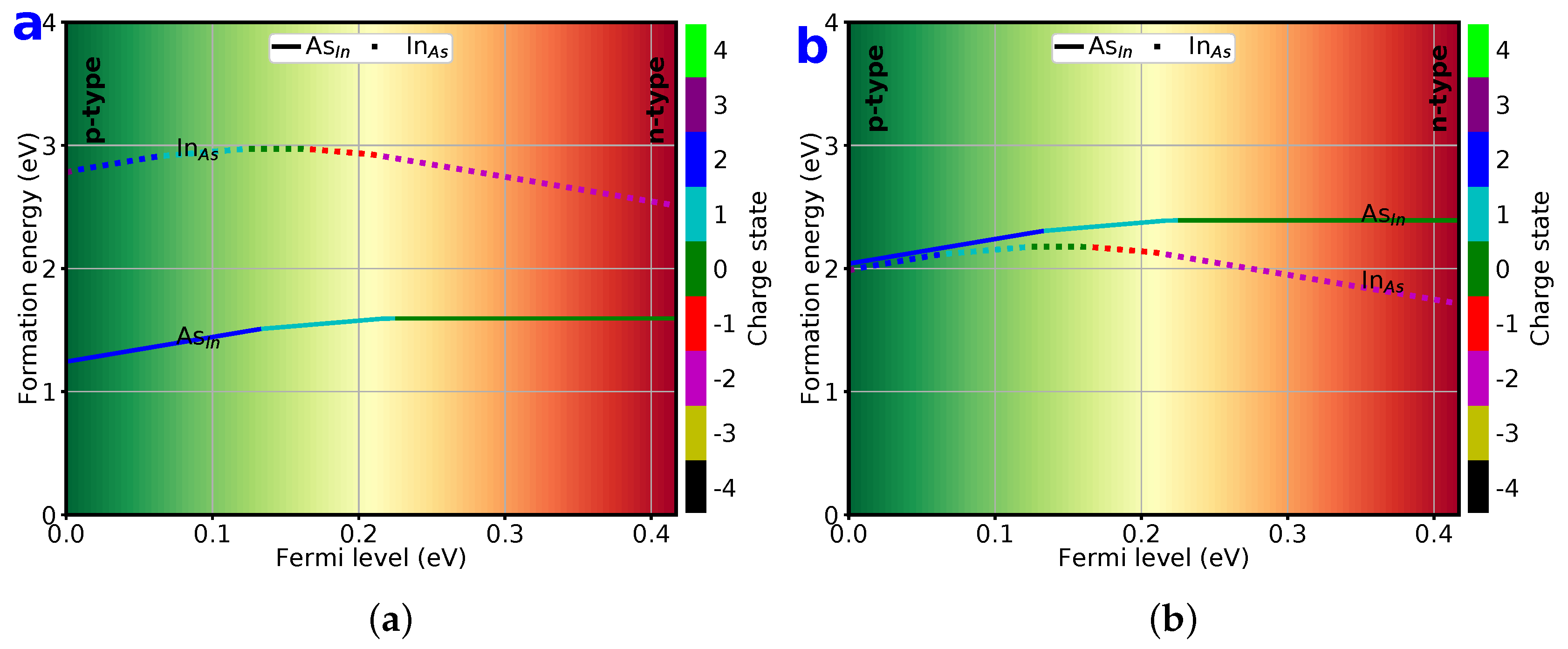
3.5. Formation Energy of Substitutionals

Next, we consider substitutional intrinsic point defects. Since we have two elements in the pristine zb-InAs, there are only two substitutional intrinsic point defects, i.e., As I n , and In A s . The formation energies of these two substitutionals as functions of E F are displayed in Figure 6 for both As-rich and In-rich chemical environments. As seen in this figure, the formation energies of substitutionals are greatly affected by chemical environment. Under an As-rich environment, As I n has a relatively low formation energy, and is at least 1 eV lower than that of In A s . This result indicates that As atoms tend to replace In atoms at In lattice sites. As a result, the As concentration will be much higher. In addition, As substitutionals favor neutral ( q = 0 ) or lower positively charged states ( q = + 1 , + 2 e ).
On the other hand, for an In-rich environment, In substitutionals are energetically favored, with its formation energy only slightly lower than that of As substitutionals. Here, the difference of formation energy between two substitutionals is much less than that in As-rich environment, implying that the difference of concentrations between substitutionals will be much less than that in As-rich environment.

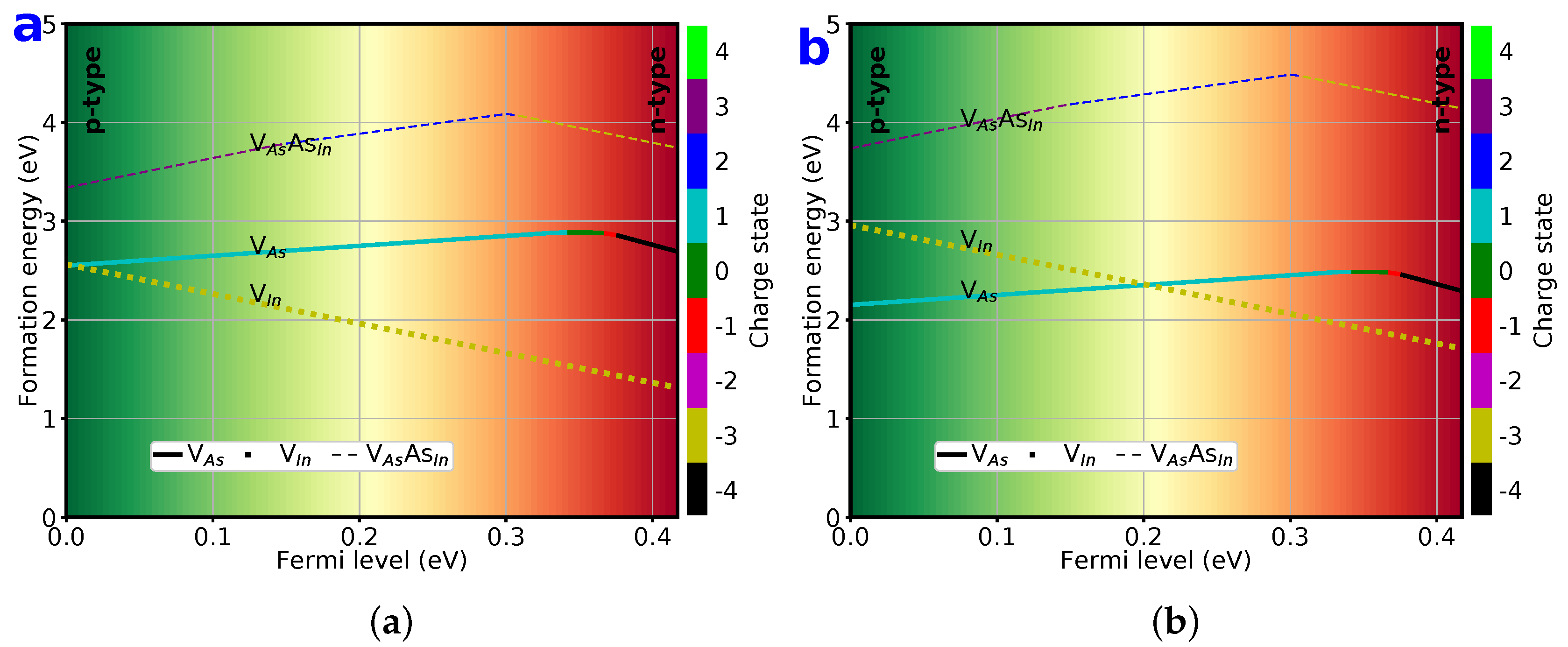
3.6. Formation Energy of Vacancies

Vacancy-type defects are known as the most common defects and play an important role in vacancy-mediated diffusion and mass transports. There are two intrinsic vacancy-type point defects in zb-InAs: V A s and V I n . We will only consider a point defect complex V A s As I n . This complex is of interest because it is closely related to V I n . When one vacancy is generated on an In atom site, one As atom on a nearest-neighbor site might dissociate from the host and fill up this vacancy site, forming the V A s As I n complex. Here, we will not consider the As counterpart of V I n In A s , since a previous study has already reported that the defect complex of V I n In A s is unstable and spontaneously relaxes back to V A s single vacancy-type defect [26].
The formation energies of three vacancies related to intrinsic defects are plotted in Figure 7 as functions of E F . For both As-rich and In-rich chemical environments, V I n decreases quickly and monotonically with increasing E F . In addition, the charge state prefers q = 3 e throughout the whole range of E F . The decrease amounts are 1.2 and 1.3 eV for As-rich and In-rich environments, respectively. Both V A s and V A s As I n have a general trend of increasing in formation energy with E F up to E F > 0.31 eV. The defect complex V A s As I n has the highest formation energy among the three vacancy defects, larger than 3 eV, indicating that this defect complex is much less favored than two single-vacancy defects.
For the As-rich environment, V I n has the lowest formation energy among three types of vacancy-related defects. The monotonic decrease of formation energy from 2.56 eV at E F = 0 to 1.35 eV at E F = 0.417 eV indicates that V I n defects are energetically favored, especially for n-type doping. For the In-rich environment, on the other hand, V A s has the lowest formation energy, till E F > 0.2 eV, implying that As vacancy becomes the dominant vacancy in p-doped In-rich zb-InAs. For n-type doped zb-InAs, In vacancy is the majority vacancy for all chemical environments.

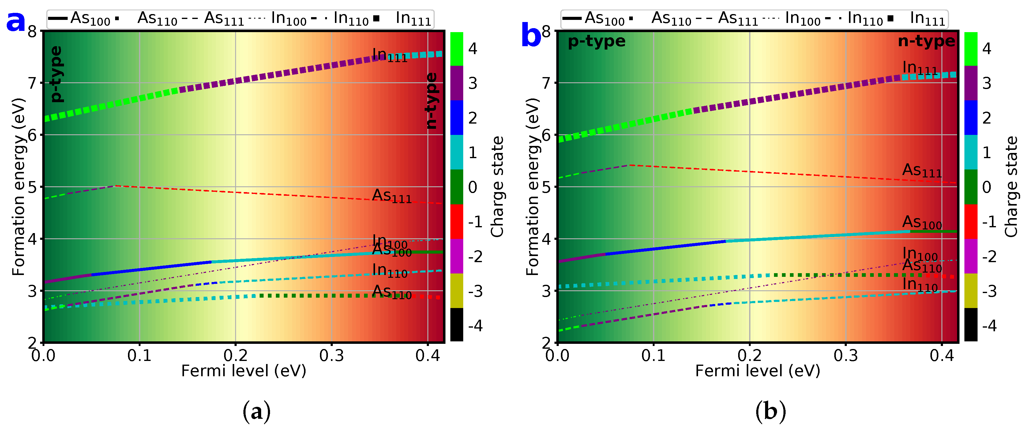
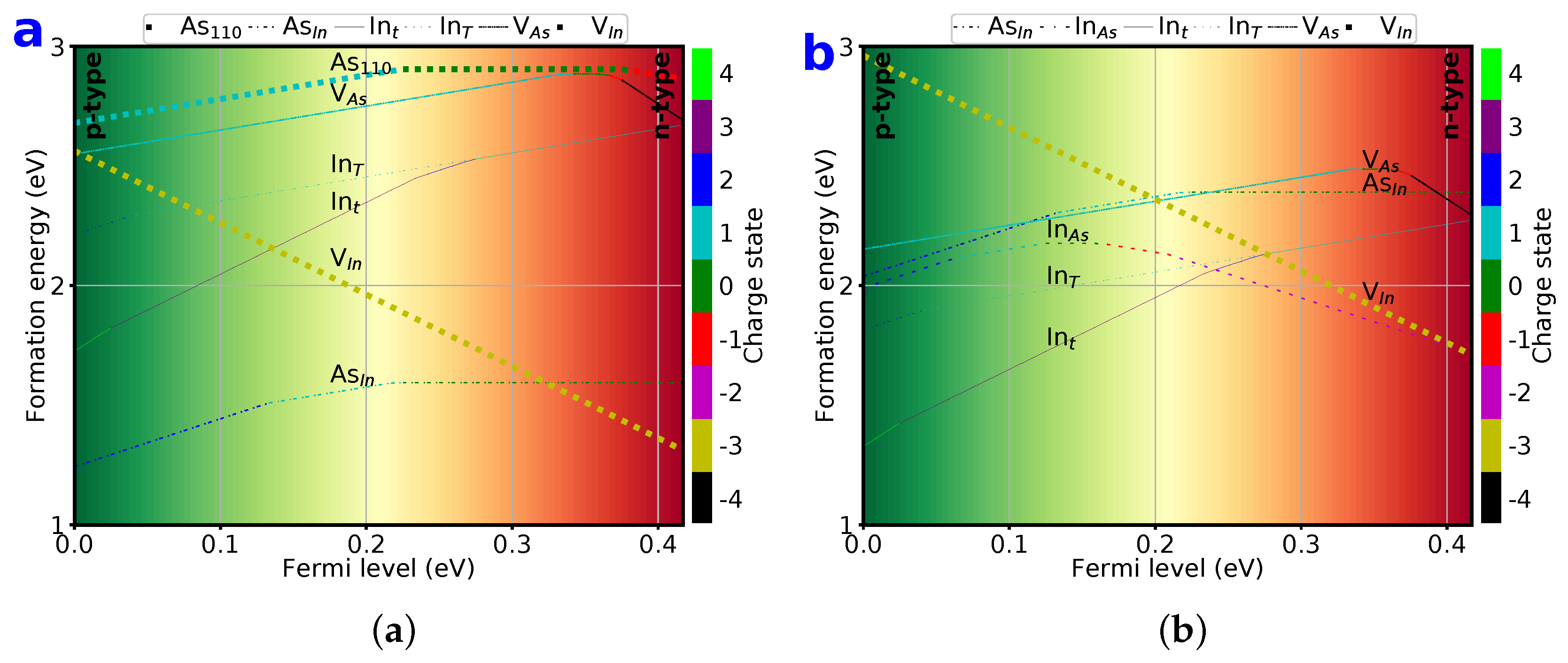
3.7. Lowest 6 Formation Energy of Point Defects

After comparison of the formation energies within each individual defect group, it is insightful to compare all fifteen intrinsic point defects as a whole. For that purpose, we plotted six lowest formation energies of fifteen defect configurations in a dilute limit as functions of E F in Figure 8 under two extreme chemical environments, i.e., As-rich and In-rich one. The six lowest formation energies ordered from low to high belongs to As I n , V I n , In t , In T , V A s , and As 110 at E F = E g / 2 = 0.209 eV at As-rich environment. The corresponding order is In t , In T , In A s , As I n , V A s , and V I n at In-rich environment.
The chemical environment greatly changes the formation energies of intrinsic point defects. Six lowest formation energies in an As-rich environment differ from those in In-rich environment for species, amount, and charge states. For As-rich environments, the lowest formation energy is 1.24 eV for As I n at E F = 0 win the charge state of q = + 2 e , and 1.59 eV for E F > 0.22 eV in the charge-neutral state. Our results qualitatively agree with an earlier report that the As I n defect has the lowest formation energy in arsenic rich environments with the same charge status but much less formation energy. [55] The discrepancy might attribute to the small supercell (only 64 atoms) in their study. The second lowest formation energy belongs to vacancy-type V I n with the formation energy as low as 1.31 eV at E F = 0.417 eV. All the other point defects have their formation energies larger than 1.6 eV, indicating much smaller concentrations than those of As I n and V I n defects.
On the other hand, for an In-rich environment, the lowest formation energies are among In tetrahedral interstitials and substitutionals. For p-type doping, In t interstitials are dominant with the lowest formation energy for E F < 0.24 eV. Actually, its smallest value is 1.33 eV at E F = 0 . When E F > 0.24 eV, the lowest formation energy among all intrinsic point defects is switched to substitutional In A s with the minimum value of 1.715 eV at E F = 0.417 eV and the charge state of q = 2 e . It is worth noting that a previous study reported that In t interstitials have lowest formation energy, ranged from 0.3 to 1.55 eV, through out the whole Fermi level. [55] The difference might be due to the much smaller system size in the previous study.
Overall, the minimum formation energy of an intrinsic point defect is predicted to be 1.24 eV in zb-InAs with As I n configuration. This is a substitutional point defect in an As-rich chemical environment with the charge state of q = + 2 e in light doping regime. The predominant substitutional point defects are expected useful in designing radiation-tolerant electronics and opto-electronics, because the ubiquitous point defects reduce the separation of Frenkel pairs, and therefore enhance the recombination of point defects under irradiation of high-energy particles. To increase the radiation resistance, it is suggested to choose an As-rich chemical environment.
As a side note, these point defects accessed via first-principles calculations here could be detected experimentally by photo-luminescence (PL) or Electron paramagnetic resonance (EPR) spectroscopy [21]. Further experimental investigations are desirable for their irradiation tolerance study.

4. Conclusions

We have systematically investigated fifteen different kinds of intrinsic point defects in single crystalline zb-InAs using a supercell method by means of first-principles calculations within the frame of density functional theory. These fifteen types of intrinsic point defects have been characterized as five groups, namely dumbbell interstitials, tetrahedral interstitials, substitutionals, vacancies, and complex. We have examined the formation energies of all of these intrinsic point defects as functions of Fermi level E F in both As-rich and In-rich chemical environments with charge states ranging from 4 e to + 4 e in the dilute-solution limit including finite-size corrections. All fifteen types of defect formation energies are found greatly affected by chemical environments. For As-rich environment, substitutional point defects are the primary intrinsic point defects in zb-InAs until the n-type doped region E F > 0.32 eV is reached, where the dominant intrinsic point defects are changed to In vacancies. For In-rich environment, In tetrahedral interstitial has the lowest formation energy till n-type doped E F > 0.24 eV region where substitutional point defects In A s take over. The < 111 > dumbbell interstitials are found unfavorable among all the point defects. However, they prefer < 110 > configurations, instead. The most interesting feature of the tetrahedral interstitials is that for both As-rich and In-rich environments, In atoms prefer the 4-As tetrahedral site In t up to E F > 0.26 eV, where In atoms acquire the same formation energy at both tetrahedral sites and the same charge state. The identical formation energies and charge states strongly suggest a fast diffusion process for In atoms along the path of t T t among various tetrahedral sites. The In-rich chemical environment greatly reduces the formation energy of In tetrahedral sites, implying much higher concentrations. In addition, V I n decreases quickly and monotonically with increasing E F , and its charge state prefers q = 3 e throughout the whole range of E F . The most popular vacancy-type defect is V I n in an As-rich environment, but switches to V A s in an In-rich environment at p-type doped region of E F < 0.2 eV. Our results shed light on relative stabilities of these intrinsic point defects, as well as their relative concentrations and possible diffusions. This study is expected very insightful in defect-engineering the zb-InAs based semiconductors, as well as material design for radiation resistant electronics and opto-electronics.

Supplementary Materials

The following are available online at https://0-www-mdpi-com.brum.beds.ac.uk/2073-4352/9/1/48/s1: Figure S1: Defect formation energy in As-rich environment, Figure S2: Defect formation energy in In-rich environment.

Author Contributions

Conceptualization, F.G., D.H. and E.R.H.; computations, Q.P. and N.C.; writing-original draft preparation, Q.P.; writing-review and editing, F.G., D.H., E.R.H., D.A.C., N.C.; supervision, F.G. and D.H.; project administration, F.G.

Funding

This research was funded by Air Force Research Laboratory (AFRL) and Air Force Office of Scientific Research (AFOSR)

Acknowledgments

The authors would like to acknowledge the generous financial support from the Air Force Research Laboratory (AFRL). D.H. would like to thank the Air Force Office of Scientific Research (AFOSR) for support.

Conflicts of Interest

There are no conflicts of interest to declare.

Data Availability

The datasets generated during and/or analyzed during the current study are available from the corresponding author on reasonable request.

References

  1. Razeghi, M. High-power laser-diodes based on ingaasp alloys. Nature 1994, 369, 631–633. [Google Scholar] [CrossRef]
  2. Kim, S.-W.; Sujith, S.; Lee, B.Y. InAsxSb1-x alloy nanocrystals for use in the near infrared. Chem. Commun. 2006, 4811–4813. [Google Scholar] [CrossRef]
  3. Marshall, A.R.J.; Tan, C.H.; Steer, M.J.; David, J.P.R. Electron dominated impact ionization and avalanche gain characteristics in InAs photodiodes. Appl. Phys. Lett. 2008, 93, 111107. [Google Scholar] [CrossRef]
  4. Chelikowsky, J.R.; Cohen, M.L. Nonlocal pseudopotential calculations for the electronic structure of eleven diamond and zinc-blende semiconductors. Phys. Rev. B 1976, 14, 556–582. [Google Scholar] [CrossRef]
  5. Gorczyca, I.; Christensen, N.E.; Alouani, M. Calculated optical and structural properties of InP under pressure. Phys. Rev. B 1989, 39, 7705–7712. [Google Scholar] [CrossRef]
  6. Chang, K.J.; Froyen, S.; Cohen, M.L. Pressure coefficients of band gaps in semiconductor. Solid State Commun. 1984, 50, 105–107. [Google Scholar] [CrossRef]
  7. Del Alamo, J.A. Nanometre-scale electronics with III-V compound semiconductors. Nature 2011, 479, 317–323. [Google Scholar] [CrossRef]
  8. Jones, K.S.; Lind, A.G.; Hatem, C.; Moffatt, S.; Ridgway, M.C. A Brief Review of Doping Issues in III-V Semiconductors. ECS Trans. 2013, 53, 97–105. [Google Scholar] [CrossRef]
  9. Dayeh, S.A.; Susac, D.A.; Kavanagh, K.L.; Yu, E.T.; Wang, D. Structural and Room-Temperature Transport Properties of Zinc Blende and Wurtzite InAs Nanowires. Adv. Funct. Mater. 2009, 19, 2102–2108. [Google Scholar] [CrossRef]
  10. Adachi, S. Properties of Semiconductor Alloys: Group-IV, III-V and II-VI Semiconductors; Wiley Online Library: Hoboken, NJ, USA, 2009. [Google Scholar]
  11. Park, H.D.; Prokes, S.M.; Cammarata, R.C. Growth of epitaxial InAs nanowires in a simple closed system. Appl. Phys. Lett. 2005, 87, 063110. [Google Scholar] [CrossRef]
  12. Dayeh, S.A.; Yu, E.T.; Wang, D. III-V nanowire growth mechanism: V/III ratio and temperature effects. Nano Lett. 2007, 7, 2486–2490. [Google Scholar] [CrossRef] [PubMed]
  13. Dick, K.A.; Deppert, K.; Martensson, T.; Mandl, B.; Samuelson, L.; Seifert, W. Failure of the vapor-liquid-solid mechanism in Au-assisted MOVPE growth of InAs nanowires. Nano Lett. 2005, 5, 761–764. [Google Scholar] [CrossRef] [PubMed]
  14. Bashouti, M.Y.; Tung, R.T.; Haick, H. Tuning the Electrical Properties of Si Nanowire Field-Effect Transistors by Molecular Engineering. Small 2009, 5, 2761–2769. [Google Scholar] [CrossRef]
  15. Dayeh, S.A.; Aplin, D.P.R.; Zhou, X.; Yu, P.K.L.; Yu, E.T.; Wang, D. High electron mobility InAs nanowire field-effect transistors. Small 2007, 3, 326–332. [Google Scholar] [CrossRef] [PubMed]
  16. Dayeh, S.A.; Yu, E.T.; Wang, D. Transport Coefficients of InAs Nanowires as a Function of Diameter. Small 2009, 5, 77–81. [Google Scholar] [CrossRef] [PubMed]
  17. Park, D.W.; Jeon, S.G.; Lee, C.-R.; Lee, S.J.; Song, J.Y.; Kim, J.O.; Noh, S.K.; Leem, J.-Y.; Kim, J.S. Structural and electrical properties of catalyst-free Si-doped InAs nanowires formed on Si(111). Sci. Rep. 2015, 5, 16652. [Google Scholar] [CrossRef] [PubMed] [Green Version]
  18. Ning, F.; Tang, L.-M.; Zhang, Y.; Chen, K.-Q. First-principles study of quantum confinement and surface effects on the electronic properties of InAs nanowires. J. Appl. Phys. 2013, 114, 224304. [Google Scholar] [CrossRef]
  19. Alam, K.; Sajjad, R.N. Electronic Properties and Orientation-Dependent Performance of InAs Nanowire Transistors. IEEE Trans. Electron Devices 2010, 57, 2880–2885. [Google Scholar] [CrossRef]
  20. Dos Santos, C.L.; Piquini, P. Diameter dependence of mechanical, electronic, and structural properties of InAs and InP nanowires: A first-principles study. Phys. Rev. B 2010, 81, 075408. [Google Scholar] [CrossRef]
  21. Repp, S.; Weber, S.; Erdem, E. Defect Evolution of Nonstoichiometric ZnO Quantum Dots. J. Phys. Chem. C 2016, 120, 25124–25130. [Google Scholar] [CrossRef]
  22. Dodd, P.E.; Massengill, L.W. Basic mechanisms and modeling of single-event upset in digital microelectronics. IEEE Trans. Nucl. Sci. 2003, 50, 583–602. [Google Scholar] [CrossRef]
  23. Ziegler, J.F.; Lanford, W.A. Effect of Cosmic Rays on Computer Memories. Science 1979, 206, 776–788. [Google Scholar] [CrossRef] [PubMed]
  24. Dick, K.A.; Caroff, P.; Bolinsson, J.; Messing, M.E.; Johansson, J.; Deppert, K.; Wallenberg, L.R.; Samuelson, L. Control of III-V nanowire crystal structure by growth parameter tuning. Semicond. Sci. Technol. 2010, 25, 024009. [Google Scholar] [CrossRef]
  25. Kim, Y.-S.; Hummer, K.; Kresse, G. Accurate band structures and effective masses for InP, InAs, and InSb using hybrid functionals. Phys. Rev. B 2009, 80, 035203. [Google Scholar] [CrossRef]
  26. Reveil, M.; Huang, H.-L.; Chen, H.-T.; Liu, J.; Thompson, M.O.; Clancy, P. Ab Initio Studies of the Diffusion of Intrinsic Defects and Silicon Dopants in Bulk InAs. Langmuir 2017, 33, 11484–11489. [Google Scholar] [CrossRef] [PubMed]
  27. Wang, J.; Lukose, B.; Thompson, M.O.; Clancy, P. Ab initio modeling of vacancies, antisites, and Si dopants in ordered InGaAs. J. Appl. Phys. 2017, 121, 045106. [Google Scholar] [CrossRef]
  28. Northrup, J.E.; Zhang, S.B. Dopant and defect energetics - Si in GaAs. Phys. Rev. B 1993, 47, 6791–6794. [Google Scholar] [CrossRef]
  29. Lee, C.-W.; Lukose, B.; Thompson, M.O.; Clancy, P. Energetics of neutral Si dopants in InGaAs: An ab initio and semiempirical Tersoff model study. Phys. Rev. B 2015, 91, 094108. [Google Scholar] [CrossRef]
  30. Lee, S.G.; Chang, K.J. Energetics and hydrogen passivation of carbon-related defects in InAs and In0.5Ga0.5As. Phys. Rev. B 1996, 53, 9784–9790. [Google Scholar] [CrossRef]
  31. Freysoldt, C.; Grabowski, B.; Hickel, T.; Neugebauer, J.; Kresse, G.; Janotti, A.; Van de Walle, C.G. First-principles calculations for point defects in solids. Rev. Mod. Phys. 2014, 86, 253–305. [Google Scholar] [CrossRef]
  32. Leslie, M.; Gillan, N.J. The energy and elastic dipole tensor of defects in ionic crystals calculated by the supercell method. J. Phys. C Solid State Phys. 1985, 18, 973. [Google Scholar] [CrossRef]
  33. Schultz, P.A. Charged Local Defects in Extended Systems. Phys. Rev. Lett. 2000, 84, 1942–1945. [Google Scholar] [CrossRef] [PubMed] [Green Version]
  34. Makov, G.; Payne, M.C. Periodic boundary conditions in ab initio calculations. Phys. Rev. B 1995, 51, 4014–4022. [Google Scholar] [CrossRef]
  35. Van de Walle, C.G.; Neugebauer, J. First-principles calculations for defects and impurities: Applications to III-nitrides. J. Appl. Phys. 2004, 95, 3851–3879. [Google Scholar] [CrossRef]
  36. Freysoldt, C.; Neugebauer, J.; Van de Walle, C.G. Fully Ab Initio Finite-Size Corrections for Charged-Defect Supercell Calculations. Phys. Rev. Lett. 2009, 102, 016402. [Google Scholar] [CrossRef] [PubMed]
  37. Lany, S.; Zunger, A. Assessment of correction methods for the band-gap problem and for finite-size effects in supercell defect calculations: Case studies for ZnO and GaAs. Phys. Rev. B 2008, 78, 235104. [Google Scholar] [CrossRef]
  38. Komsa, H.-P.; Rantala, T.T.; Pasquarello, A. Finite-size supercell correction schemes for charged defect calculations. Phys. Rev. B 2012, 86, 045112. [Google Scholar] [CrossRef]
  39. Castleton, C.W.M.; Höglund, A.; Mirbt, S. Managing the supercell approximation for charged defects in semiconductors: Finite-size scaling, charge correction factors, the band-gap problem, and the ab initio dielectric constant. Phys. Rev. B 2006, 73, 035215. [Google Scholar] [CrossRef]
  40. Taylor, S.E.; Bruneval, F. Understanding and correcting the spurious interactions in charged supercells. Phys. Rev. B 2011, 84, 075155. [Google Scholar] [CrossRef]
  41. Kresse, G.; Hafner, J. Ab initio molecular dynamics for liquid metals. Phys. Rev. B 1993, 47, 558–561. [Google Scholar] [CrossRef]
  42. Kresse, G.; Furthuller, J. Efficiency of ab-initio total energy calculations for metals and semiconductors using a plane-wave basis set. Comput. Mater. Sci. 1996, 6, 15–50. [Google Scholar] [CrossRef]
  43. Hohenberg, P.; Kohn, W. Inhomogeneous electron gas. Phys. Rev. 1964, 136, B864. [Google Scholar] [CrossRef]
  44. Kohn, W.; Sham, L.J. Self-consistent equations including exchange and correlation effects. Phys. Rev. 1965, 140, A1133. [Google Scholar] [CrossRef]
  45. Perdew, J.P.; Burke, K.; Ernzerhof, M. Generalized Gradient Approximation Made Simple. Phys. Rev. Lett. 1996, 77, 3865–3868. [Google Scholar] [CrossRef] [PubMed]
  46. Perdew, J.P.; Ruzsinszky, A.; Csonka, G.I.; Vydrov, O.A.; Scuseria, G.E.; Constantin, L.A.; Zhou, X.; Burke, K. Restoring the density-gradient expansion for exchange in solids and surfaces. Phys. Rev. Lett. 2008, 100, 136406. [Google Scholar] [CrossRef]
  47. Blöchl, P.E. Projector augmented-wave method. Phys. Rev. B 1994, 50, 17953–17979. [Google Scholar] [CrossRef] [Green Version]
  48. Jones, R.O.; Gunnarsson, O. The density functional formalism, its applications and prospects. Rev. Mod. Phys. 1989, 61, 689–746. [Google Scholar] [CrossRef]
  49. Bechstedt, F.; Belabbes, A. Structure, energetics, and electronic states of III-V compound polytypes. J. Phys. Condens. Matter 2013, 25, 273201. [Google Scholar] [CrossRef] [PubMed]
  50. Tahini, H.A.; Chroneos, A.; Murphy, S.T.; Schwingenschlögl, U.; Grimes, R.W. Vacancies and defect levels in III–V semiconductors. J. Appl. Phys. 2013, 114, 063517. [Google Scholar] [CrossRef] [Green Version]
  51. Madelung, O.; Schulz, M.; Weiss, H. (Eds.) Semiconductors, Physics of Group IV Elements and III-V Compounds; Springer-Verlag: New York, NY, USA, 1982; Volumn 17. [Google Scholar]
  52. Shu, H.; Liang, P.; Wang, L.; Chen, X.; Lu, W. Tailoring electronic properties of InAs nanowires by surface functionalization. J. Appl. Phys. 2011, 110, 103713. [Google Scholar] [CrossRef]
  53. Thompson, A.G.; Rowe, J.E.; Rubenste, M. Preparation and Optical Properties of InAs1-xPx Alloys. J. Appl. Phys. 1969, 40, 3280–3288. [Google Scholar] [CrossRef]
  54. Dreyer, C.E.; Alkauskas, A.; Lyons, J.L.; Janotti, A.; Van de Walle, C.G. First-Principles Calculations of Point Defects for Quantum Technologies. Annu. Rev. Mater. Res. 2018, 48, 1–26. [Google Scholar] [CrossRef]
  55. Höglund, A.; Castleton, C.W.M.; Göthelid, M.; Johansson, B.; Mirbt, S. Point defects on the (110) surfaces of InP, InAs, and InSb: A comparison with bulk. Phys. Rev. B 2006, 74, 075332. [Google Scholar] [CrossRef]
Figure 1. Atomic structures of pristine zinc blende InAs in (a) conventional unit cell with 4 In and 4 As atoms and (b) 3 × 3 × 3 super unit cell with 108 In and 108 As atoms, referenced for defect calculations. Here, the small yellow ball denotes As atoms, while the large silver balls are for In atoms.
Crystals 09 00048 g001
Figure 2. The atomic structures of 15 intrinsic point-defect configurations of zb-InAs after full geometry optimization according to the minimum energy in neural charge state: (a) As 100 , (b) As 110 , (c) As 111 , (d) As t , (e) In 100 , (f) In 110 , (g) In 111 , (h) In T , (i) As I n , (j) V A s , (k) As T , (l) V A s As I n , (m) In A s , (n) V I n , (o) In t . Here, the small yellow spheres denote As atoms, while the large silver spheres denotes In atoms.
Crystals 09 00048 g002
Figure 3. Formation energies as functions of E F in the As-rich (a) and In-rich (b) environments for fifteen different types of point defects in zb-InAs with all possible charge states from −4 to +4 + e . The different doping regimes near valance bands (p-type) and conduction bands (n-type) are displayed.
Crystals 09 00048 g003
Figure 4. Formation energies as functions of E F under (a) As-rich and (b) In-rich environment for six labeled dumbbell type point defects in zb-InAs with all possible charge states from 4 to + 4 marked with different colors.
Crystals 09 00048 g004
Figure 5. Formation energies as functions of E F in the (a) As-rich and (b) In-rich environment for four tetrahedral-site interstitial type point defects in zb-InAs with all possible charge states from 4 to + 4 marked with different colors. The y-axises are enlarged for viewing details.
Crystals 09 00048 g005
Figure 6. Formation energies as functions of E F in the (a) As-rich and (b) In-rich environment for two substitutional type point defects in zb-InAs with all possible charge states from 4 to + 4 marked with different colors.
Crystals 09 00048 g006
Figure 7. Formation energies as functions of E F in the (a) As-rich and (b) In-rich environment for two vacancy-type point defects in zb-InAs with all possible charge states from 4 to + 4 marked with different colors.
Crystals 09 00048 g007
Figure 8. Six lowest defect formation energies in zb-InAs as functions of E F in the (a) As-rich and (b) In-rich environment with all possible charge states from 4 to + 4 marked by corresponding colors.
Crystals 09 00048 g008

