1. Introduction
Strontium titanate (SrTiO
3), designated from here on as STO, is a very useful multifunctional ceramic material exhibiting remarkable and fascinating physical and chemical properties. This paradigmatic example of oxide perovskites has a high potential for electrical, optoelectronic, photocatalytic, and magnetic applications, and constitutes a basis for the so-called complex oxide-based microelectronics [
1,
2,
3,
4,
5]. Moreover, STO is a model transition metal oxide material with a simple crystal structure that serves as a reference to understand the behavior of all other oxide perovskites, such as BaTiO
3, KTaO
3, and PbTiO
3. To advance the understanding and mastering of all these applications, it is essential to improve our knowledge on crystal defects and electronic carrier behavior in this material. In spite of the extensive research work performed during many years and the progress achieved, there are still many key problems waiting for a solution. The authors of this review, together with a number of active research groups around the world, have been recently involved in this task, and a summary of their main achievements in the field appears opportune. The paper focusses on the use of luminescence experiments to elucidate some of the key challenges, related to the localization of electronic carriers [
6,
7,
8,
9] and excitons, as well as the structure of oxygen vacancies and their capabilities for electron/polaron trapping. A main technique used to address this complex problem is ion beam induced luminescence or ionoluminescence (IL) that combines the capabilities of ion beams to generate point defects through elastic atom collisions with the high sensitivity of luminescence spectroscopy to identify and characterize them. In fact, the identification of oxygen vacancies by their luminescence emission has been a conflictive issue during all this time [
10,
11]. It appears now to be definitely established that these vacancies emit a red luminescence band centered at around 2.0 eV that is associated with trapped Ti
3+ polarons in the close vicinity of the vacancy. Abundant theoretical support for this model has been also recently achieved [
12,
13,
14,
15]. Another relevant output of recent research carried out with both pulsed lasers and ion beams has to do with the self-trapped exciton [
16,
17,
18]. New results suggest that, aside from the well-known localized green optical transition centered at 2.5 eV, the blue emission at 2.8 eV is associated with transitions from conduction band (CB) states to the ground STE level. It is expected that those new results could be further investigated and extended to other perovskite oxides.
Although the review focuses on the behavior of bulk crystals one should remark that the surfaces often present very peculiar properties and physical-chemical behavior. In particular, they may show nontrivial atomic and electronic structures including dangling bonds and incomplete atomic coordination. If these structures can be controlled, unusual charge states, and electrical and magnetic performances can be achieved, such as a high-mobility 2-D electron gas [
19]. More relevant for our review are the studies based on the monitoring of oxygen vacancy defects and Ti
3+ states at the surfaces and its impact on the luminescence behavior [
20,
21]. However, it is important to mention that the luminescence spectra and behavior observed under different excitation sources from UV light [
10,
17,
22,
23,
24,
25,
26,
27,
28,
29,
30] to X-rays [
16], electrons [
31], and ion beams [
5,
32], having very different penetration depths, show a similar pattern apparently associated to a bulk response. In spite of these considerations, we believe that surface luminescence is beyond the scope of our review and deserves independent attention.
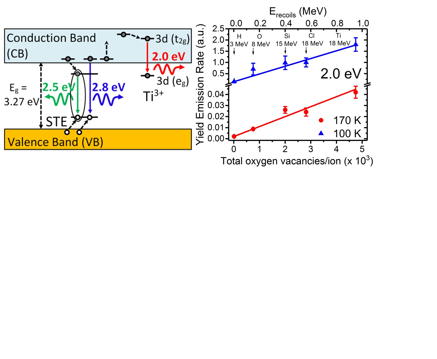
2. Crystal Structure and Main Properties of STO
Strontium titanate (STO) is an extensively studied oxide with a cubic perovskite structure ABO
3 at room temperature (RT) (space group
Pm3m) with a lattice parameter of 0.3905 nm and a density of ρ = 5.12 g/cm
3;
A is generally a monovalent (Na, K, …) or divalent (Sr, Ba, …) ion, and
B is a tetravalent (Ti, Zr, …) or pentavalent (Nb, Ta, …) ion. The crystal structure, sketched in
Figure 1, is made up of BO
6 octahedral units arranged in a cubic pattern and linked together by shared oxygen ions at the corners. The Ti
4+ ions are six-fold coordinated by O
2− ions, whereas each of the Sr
2+ ions is surrounded by four TiO
6 octahedra. Therefore, each Sr
2+ ion is coordinated by 12 O
2− ions. Within the TiO
6 octahedra, while a hybridization of the O
2p states with the Ti
3d states leads to a pronounced covalent bonding [
33], Sr
2+ and O
2− ions exhibit ionic bonding character. Hence, STO has mixed ionic-covalent bonding properties. The nature of this chemical bonding leads to a unique structure that makes it a model electronic material.
Table 1 shows the main physical properties of STO.
The stoichiometric composition of STO behaves as a wide-band gap semiconductor. Detailed measurements of the optical absorption below the fundamental edge shows an indirect transition, Γ→X, at 3.27 eV; whereas the first direct transition, X→X, is found at 3.47 eV [
34]. A large number of experimental and theoretical studies of the electronic band structure have since been performed [
35,
36]. The empty conduction band is made up mainly of Ti
3d states; whereas the valence band largely comes from O
2p states. At RT it presents a high dielectric constant (≈300 at RT and ≈20,000 near T = 0 K) [
37] and remains paraelectric at all temperatures due to a frustrated ferroelectric transition as a consequence of quantum fluctuations [
38]. At 105 K, cubic STO undergoes a structural phase transition to a tetragonal crystal structure (a = b ≠ c and c
max = 0.39 nm; space group
I4/mcm) due the opposite rotation of neighboring oxygen octahedra [
39]; whereas at lower temperatures (36 K and 65 K), it presents also some dynamic transitions that are strongly dependent on impurity doping [
40,
41].
3. Luminescence Experiments
Although many different techniques have been used to advance the understanding of the electronic structure in STO, we will focus here on luminescence experiments that have played a major role for the main achievements discussed in the present review. In particular, they have provided valuable information about the occurrence of
in-gap levels for self-trapped carriers and excitons, as well as for key impurities and defects (e.g., oxygen vacancies). A variety of excitation sources, including X-rays, electrons and ion-beams have been used for comparison (see Table 1 in [
32]). Depending on sample, excitation conditions, and measuring temperature, several overlapped Gaussian emissions centered at 2.0 eV, 2.5 eV, and 2.8 eV are generally distinguished [
32]. Remarkably, the (red) 2.0 eV band has only been clearly observed for heavily strained and amorphous samples suggesting that it is closely related to structural disorder [
31,
42,
43]. Another band at 3.2 eV has been identified at low temperatures (below 100 K) but it has not been much investigated. The interpretation of the main bands at 2.5 eV and 2.8 eV in terms of
in-gap levels associated to definite electronic centers, such as self-trapped carriers or lattice defects, has been the object of extensive research during recent years. The most used technique is photoluminescence (PL), which has been crucial in the study of self-trapped carriers and excitons. As to light excitation, continuous UV lasers [
10], as well as pulsed laser of ns [
22,
23] and ps [
24,
25,
28,
30] duration having energies slightly above the STO band gap, have been used and have provided a substantial amount of information. The power excitation densities in the ps experiments are quite high (0.01–10 mJ/cm
2), which has relevant consequences on the results. PL experiments have allowed reliable information to be obtained on key parameters of the investigated centers, such as lifetimes, electron–phonon coupling and so on, which will be discussed in the following sections.
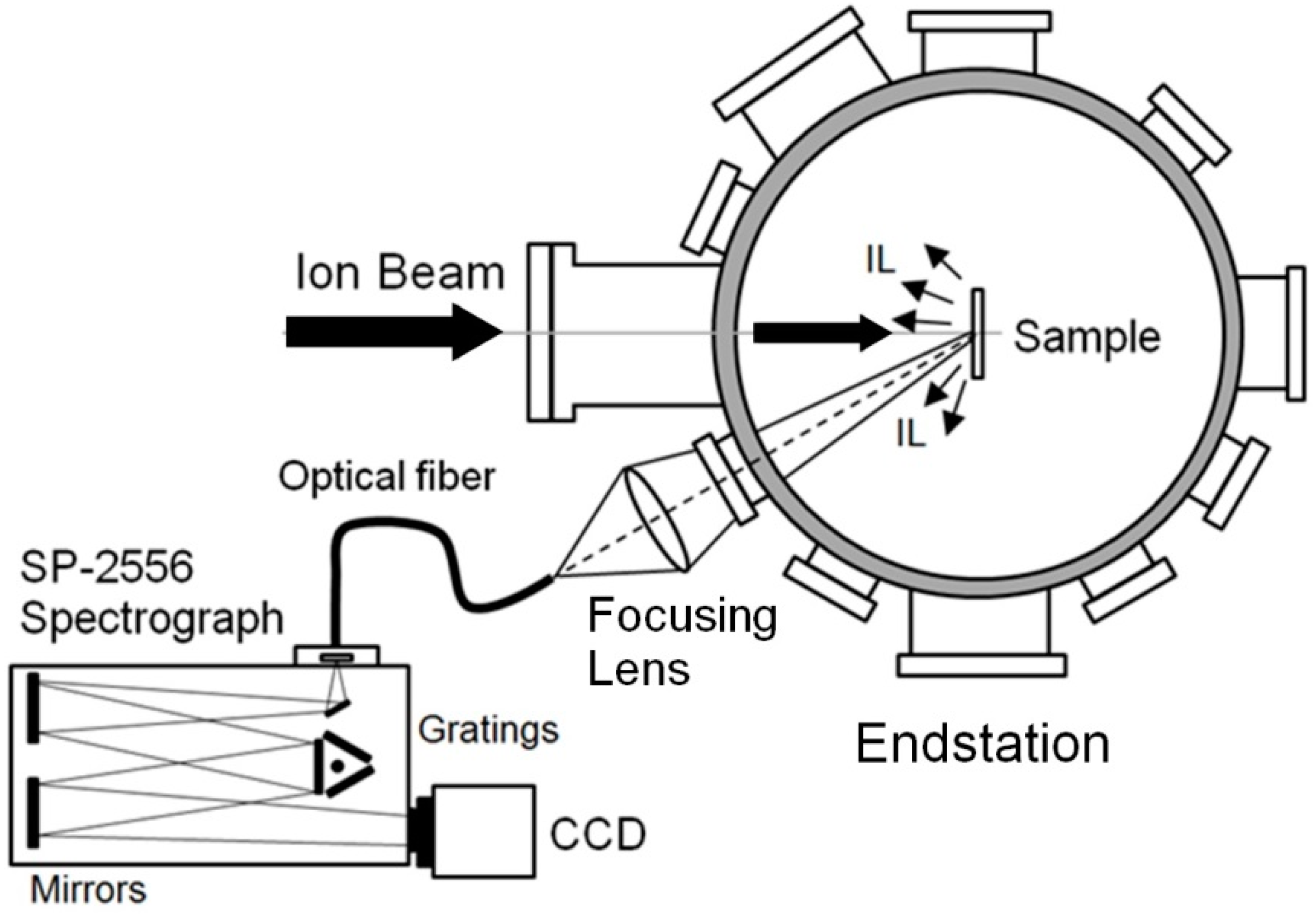
More recently, ion-beam excitation to detect the emitted ionoluminescence (IL) has been more extensively used. It presents a number of advantages over PL using continuous or pulsed lasers, such as the very large range of electronic excitation allowing for the simultaneous observation of all emission bands. In particular, this feature permits the real-time study of the interplay among all emitting centers during irradiation. The main shortcoming is the need for sophisticated installations not always available. Fortunately, reliable electrostatic accelerators in the MV range are now dedicated to this topic [
44,
45]. The proper choice of ions with different masses and energies allows controlling the relative strength of electronic excitation and atomic collision processes, as well as the penetration depth of the excitation and structural damage [
46,
47,
48]. As an example, a diagram of the installation available in the Ion Beam Materials Laboratory (IBML) at the University of Tennessee, Knoxville, TN, USA [
45,
49,
50] is shown in
Figure 2.
4. In-Gap Levels Associated to Self-Trapped Carriers (Small Polarons)
Strontium titanate and other perovskites can exhibit very high electrical conductivities and carrier mobilities. The largest mobilities can be achieved in epitaxial thin films produced by molecular beam epitaxy, which allows for precise control of structural perfection and doping concentration. In fact, electron mobilities exceeding 30,000 cm
2·V
−1·s
−1 have been obtained for epitaxial STO films at low temperatures [
51]. Furthermore, superconductivity below 1 K has been observed in STO [
52]. However, electronic transport is strongly affected by the high dielectric constant of STO and the subsequent coupling (interaction) of electronic carriers with polar phonons. The dragging of the coupled phonon cloud generally limits the mobility, turning the free carriers into the so-called large polarons with larger effective masses. Under strong electron–phonon coupling, the carriers may become localized at the atomic level and form small radius defects in accordance with the early prediction in the seminal paper by Landau [
53]. This self-trapping process is determined by a competition between the energy loss due to localization and the energy gain associated with the electron-phonon interaction and associated polarization energy [
6]. Experimental evidence for the existence of small polarons in some perovskites, such as potassium tantalate (KTaO
3) crystals, is already available, mostly through electron paramagnetic resonance spectroscopy (EPR) experiments [
54]. For electrons in STO, there is no experimental evidence for isolated small polaron states, although it has been suggested [
6,
17,
55,
56] that electron–polarons may be coupled to impurities or lattice defects. A density functional theory (DFT) approach to investigate the competition between large and small polarons has been reported [
8]. Those authors claim that for a density of electronic carriers above ≈ 10
20 cm
−3 the excess electrons tend to form small polarons; whereas smaller densities lead to delocalized electrons or large polarons. In many cases, these polaron states are expected to introduce energy levels in the forbidden gap that should be responsible for luminescence emissions. The experimental information is very extensive, although the situation is, in many cases, quite controversial and unclear. However, it seems, as described in
Section 6, that electron self-trapping at oxygen vacancies is firmly established on experimental and theoretical grounds.
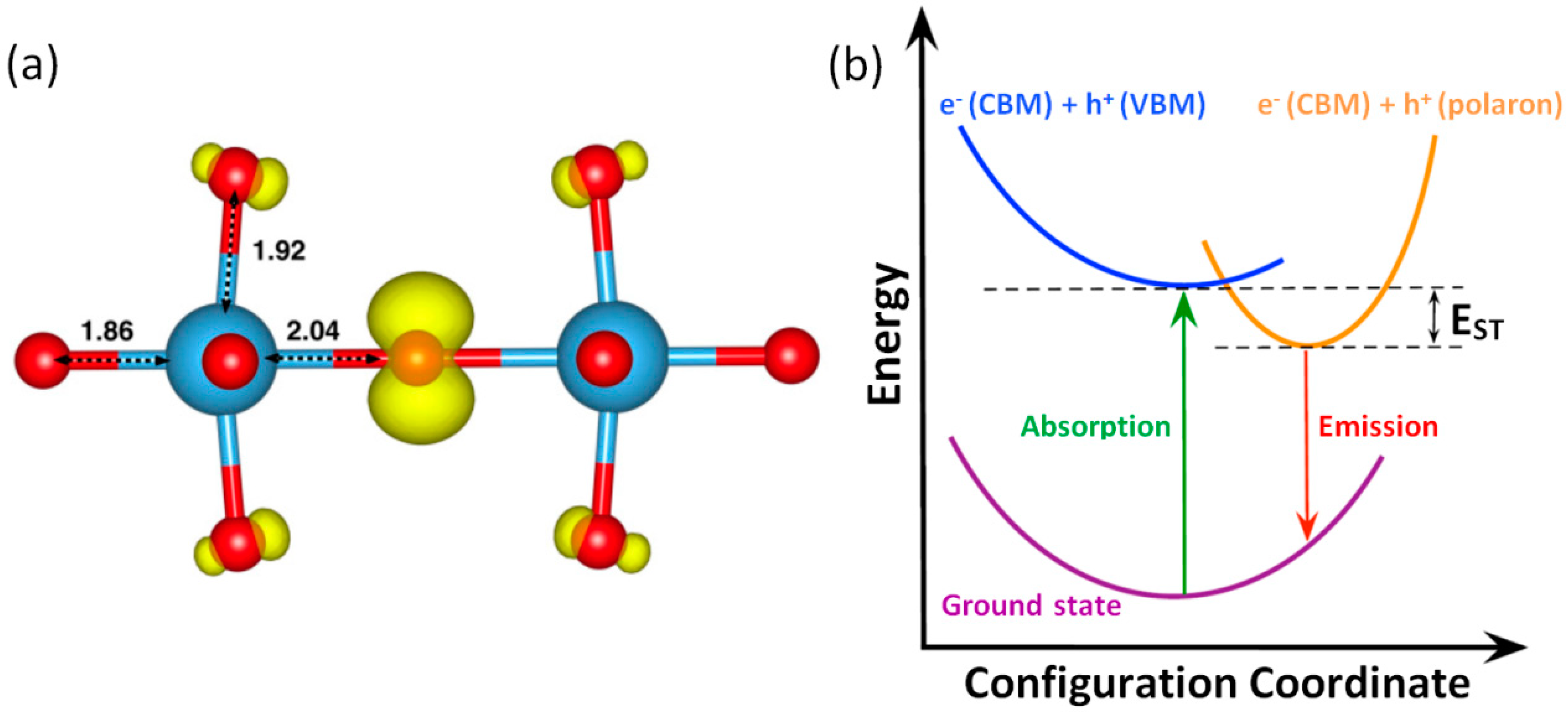
On the other hand, the question of hole self-trapping in STO looks similar to the case for electrons, i.e. no definitive experimental proof is available. However, the existence of a certain
in-gap level associated with self-trapped holes (hole-polaron,
) has been theoretically predicted [
57]. In fact, it has been calculated that holes become localized on an individual
atom with an energy decrease of 13 meV (hole self-trapping energy,
EST) with respect to a free (delocalized) hole residing at the valence-band maximum (VBM) (see
Figure 3). On the other side, the activation energy for hole hopping has been estimated to be 66 meV [
57,
58]. This makes the mobility of the hole at RT, derived from an adiabatic hopping approach, around three orders of magnitude lower compared to that for electrons (5 × 10
−3 cm
2·V
−1·s
−1 for the hole mobility, versus 10 cm
2·V
−1·s
−1 for the electron mobility [
59,
60]). Finally, it has been established that, despite the large local distortion of the lattice, the formation of a
peroxide anion, coming from two paired neighboring
anions, is energetically more favorable than two separated
ions, by ~496 meV [
57].
Aside from those calculations, the research on the topic of carrier self-trapping has focused on the role of the intrinsic
in-gap levels to account for the luminescence emissions [
8]. Interesting results have been obtained on undoped and electron-doped STO by time-resolved spectroscopy using ps pulsed lasers at several temperatures from 10 K to 700 K [
24,
25,
27,
28,
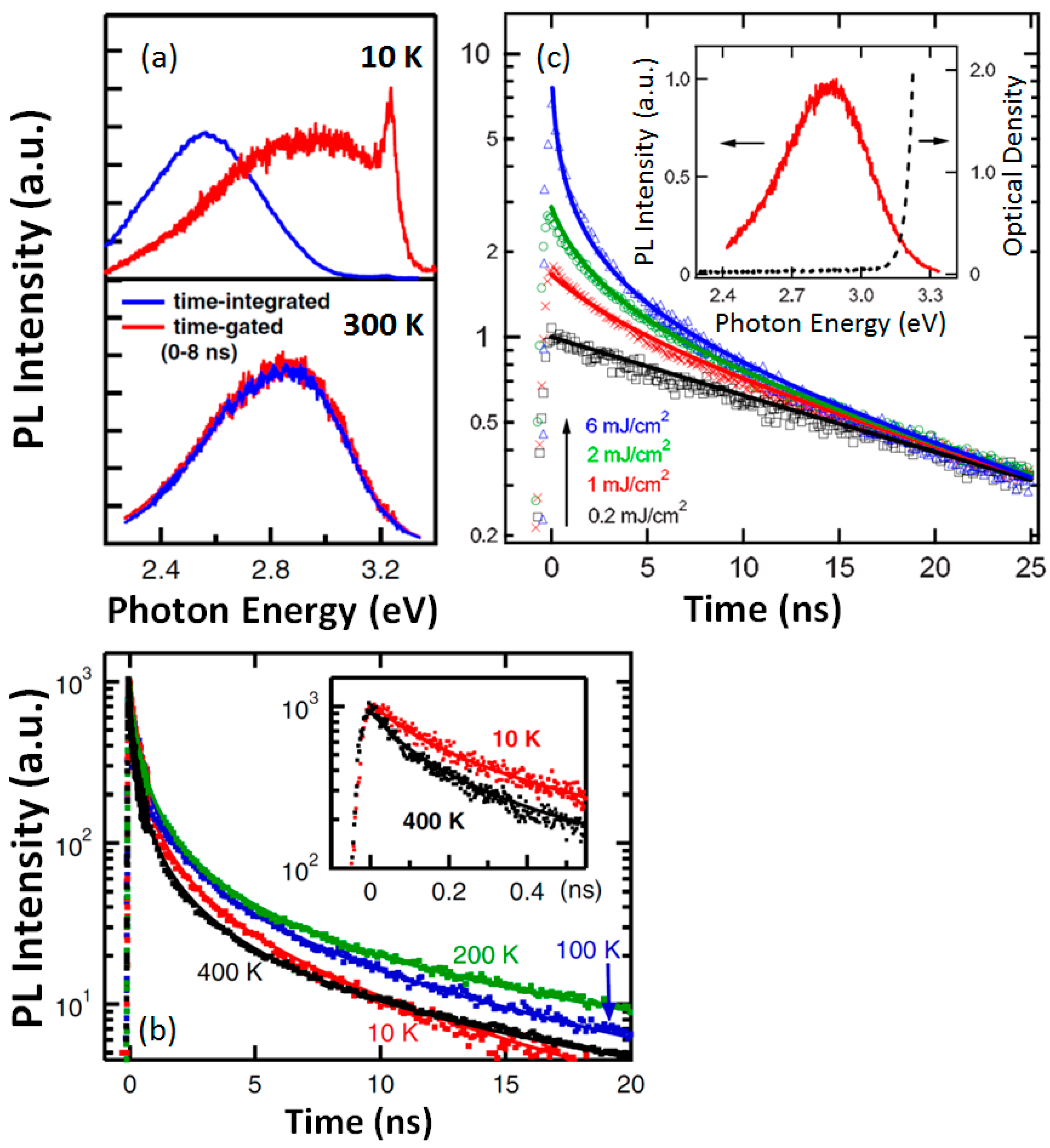
30]. They have shown that for excitation with energies slightly above the band gap, the wavelength spectra are strongly dependent on the time elapsed after the light pulse. As shown in
Figure 4, the emission during the first few nanoseconds occurs mostly in the blue region and shows a broad band centered at around 2.8 eV. At longer times, it shifts to the green region and gives rise to a broad emission PL peaked at 2.5 eV, suggesting an interplay between two trap levels at different depths after excitation. In fact, the kinetics of the emission has been described in terms of a parallel contribution of monomolecular (linear in the carrier density) and bimolecular (quadratic in the carrier density) recombination processes. A cubic process associated with non-radiative Auger transitions has been also proposed [
28], and its contribution to the kinetics of the emission yield has been quantitatively analyzed. However, this assignment has been also refuted by Rubano et al. [
27] with a quite through data analysis. It is worth mentioning that the analysis of the experiments is difficult due to the heavy overlapping between the two contributing emission bands. Therefore, the origin of the Auger processes, and their unambiguous correlation with the corresponding photon transitions, has not been possible. In summary, in accordance with previous work [
28], the data [
28] point to a trapped hole, either self-trapped or trapped at certain defects, as one of the recombining species for the 2.8 eV emission. All those experiments [
24,
25,
27,
28,
30], indeed, confirm time-resolved PL spectroscopy as an efficient route to clarify the origin of the emissions.
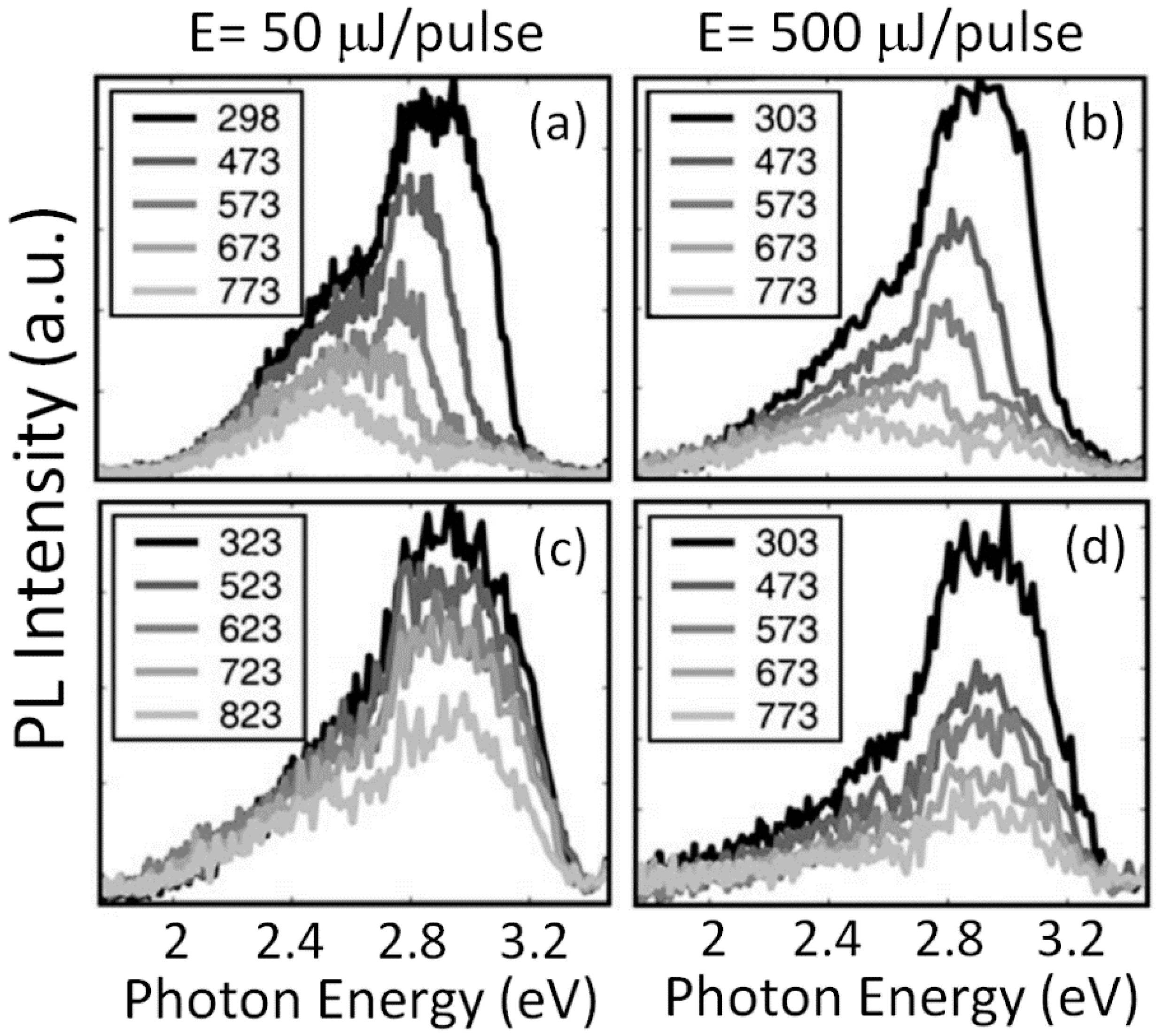
The dependence of the PL emission spectra induced by above-gap excitation on excitation rate has provided a relevant piece of information [
30]. UV pulses with a duration of 25 ps (full width at half maximum, FWHM) and photon energy of 3.49 eV have been used for exciting well above the optical direct absorption edge (about 3.4 eV) of STO [
34,
61]. The excitation rates varied from 50 μJ/pulse to near 1000 μJ/pulse. For pure stoichiometric STO, the clear evolution of the PL spectra shape is shown in
Figure 5 for irradiations at different temperatures and excitation rates. At RT, a large enhancement in the emission centered at 2.8 eV, in comparison to that at 2.5 eV, is observed for increases in pulse energy from 50 to 500 μJ per pulse: a 40% enhancement for pure STO and a 25% enhancement for Nb-doped STO. Moreover, at any of the pulse energies, the ratio between the two intensities at 2.8 eV and 2.5 eV is clearly enhanced for STO:Nb samples as well, where an excess of free electrons in the conduction band (CB) has been introduced. All these PL data have found strong support in the new IL experiments described in
Section 5, which also add new insights on a definite interpretation for the green and blue emission mechanisms.
To finish up this topic, one may briefly comment on the possible origin of the luminescence emission at 3.2 eV [
10,
29,
62]. This asymmetric non-Gaussian UV band has been reported for low temperatures (<100 K) and very high excitation rates, as well as for electron-doped samples. In both cases, the key point is the generation of high populations of excited electrons and holes. Consequently, it is reasonable to consider that the corresponding optical transition connects conduction band (CB) states and a possible
in-gap level for the self-trapped hole. In fact, theoretical estimates for the self-trapping energy of a hole yield 13 meV [
57], which may explain the very close value of the transition energy (3.2 eV) to the STO band gap energy (3.27 eV) as well as the strong reduction of the emission yield with increasing temperature.
5. Self-Trapped Excitons (STEs): Structure and Luminescence Emission
Initially, electronic excitations with energies above the band gap generate free electrons and holes. The experimental results on the time evolution of the visible and ultraviolet (VIS-UV) PL emission indicate that these free carriers very rapidly become bound into
e–h pairs localized in the lattice, forming a self-trapped exciton (STE). The trapping time to form STE bound states is in the sub-nanosecond time scale [
30]. This self-trapping effect seems dominant in pure samples over extrinsic electron or hole trapping at impurities, particularly at high excitation rates, such as those achieved under ps laser or ion-beam excitation. One may think of the STE as an electron orbiting around a self-trapped hole (or vice-versa). It has been generally accepted that the
e–h radiative recombination of the STE gives rise to a broad green emission at around 2.5 eV accompanied by strong lattice relaxation, associated with a triplet–singlet transition of the center (
–) inside a regular octahedron [
16]. The main reason is due to the large Stokes shift between the excitation (energy above the band gap) and the emission wavelengths. A similar broad green emission has been also reported for other perovskites and also assigned to STEs. A very detailed study of such emissions in STO was carried out by Leonelli and Brebner [
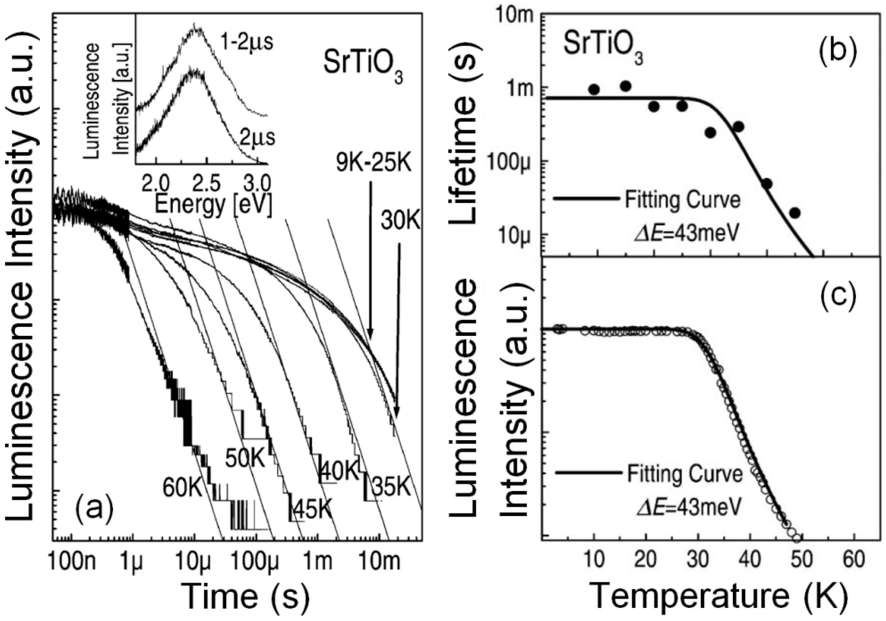
17]. They accounted for some spectroscopic parameters, such as band width, in terms of electron–phonon interaction for a localized center. The mean lifetime is quite constant, around 1 ms below 30 K, in accordance with the spin-forbidden character of the transition [
17,
22,
62]. It strongly decreases upon increasing temperature with an activation energy of 70 meV. More recently, rather similar results, plotted in
Figure 6, were obtained by Hasegawa et al. [
22,
23], suggesting a non-radiative recombination channel having a thermal activation energy of 43 meV [
22]. The measured activation energy values could be possibly related to electron–phonon interactions since they are not far from the vibronic level separation ħΩ = (88 ± 4) meV in the Huang–Rhys model for the localized center [
17]. Nonetheless, the thermal decay of the STE is not simple and cannot be described by a single exponential kinetics. In fact, researchers [
22,
23] have reported decay kinetics following a power law time dependence
(see
Figure 6), suggesting that the process may be governed by random tunneling. However, the specific physical mechanism and the involved centers in the tunneling and recombination process are not clear yet. One should remark that, assuming the adiabatic small-polaron hopping mechanism, the hole-polaron mobility has an activation energy of 66 meV [
57]. Therefore, one might think of the hopping process as hole migration to the STEs, followed by charge and energy transfer between the STE and the hole. In our opinion this problem is still waiting for a solution.
Recently, some novel ionoluminescence experiments have been performed by the authors at University of Tennessee, Knoxville, TN, USA [
45] on stoichiometric STO. The still unpublished results have shown that the emission yields for the green (
YG) and blue (
YB) bands, centered at 2.5 eV and 2.8 eV respectively, evolve in parallel during ion irradiation, and suggest that the two emission bands may originate from optical transitions from the same center, namely the STE. This scheme is reinforced by the comparison of the luminescence emissions obtained by using ions with different masses and energies, i.e., varying the electronic excitation rate. Whereas irradiations with 3 MeV H, or 8 MeV O (low electronic excitation) show a comparable contribution to the 2.8 eV and 2.5 eV emissions, the blue band is very strongly enhanced when irradiating with more energetic and heavier ions, presenting a higher electronic excitation rate. These results indeed support the models [
10,
11,
27,
30] attributing the blue emission to recombination of conduction band electrons with self-trapped holes, and establish an interesting connection between this recombination and the localized
e–h transitions for the STE. Moreover, the ion-beam results on using different ion energies, closely resemble those obtained under ps pulsed laser excitation by Rubano et al. [
27,
30], and previously shown in
Figure 5. The role of the time elapsed after a laser pulse on the emission spectra [
24,
28] can be understood as the result of the competition between the lifetimes for the green and blue overlapped bands. The long decay time of milliseconds (long lifetime) for the 2.5 eV band in comparison with the very short lifetime (a few nanoseconds) for the 2.8 eV band, explains the initial dominance of this latter emission immediately after the laser pulse excitation (see
Figure 4).
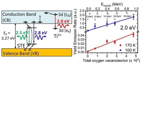
6. Point Defects in Bulk STO: Oxygen Vacancies
The oxygen vacancy is possibly the most conspicuous point defect in STO, as well as in many oxides. Many of the outstanding properties of these materials are not yet fully understood, but critically rely on the role of oxygen vacancy disorder and its effect on the electronic structure. Therefore, identification and characterization of this disorder has been a critical objective of materials scientists in order to achieve a wide range of functional applications, including manufacturing novel devices and engineering nanoscale structures.
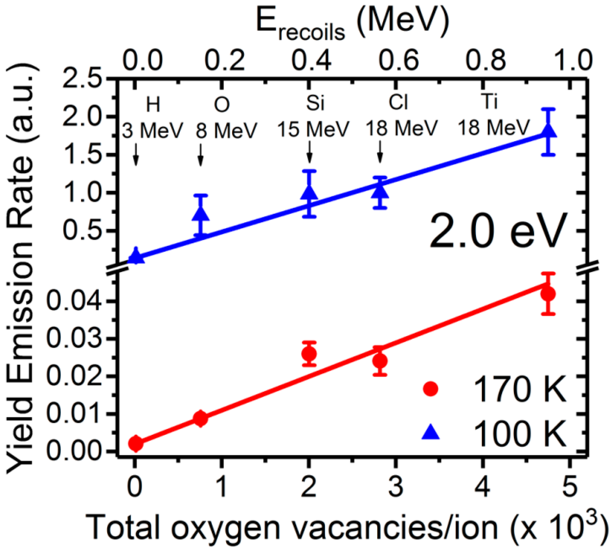
Although oxygen vacancies can be produced by different methods, such as chemical doping, thermal treatments and irradiation with particles (electrons, ions, and neutrons), their identification in STO has remained elusive from optical and EPR characterization methods. Recently, a detailed kinetic study using ion beams has allowed unambiguously assigning a red emission band centered at 2.0 eV to oxygen vacancies. The experiments [
9] have used a variety of ion beams and energies to tailor the electronic excitation rate and introduce controlled amounts of lattice defects, mainly oxygen vacancies. Furthermore, the penetration depth can be varied from less than one micron to tens of microns, so that surface effects can be minimized, in contrast to low energy cathodoluminescence (CL) or UV light excitation [
46,
47,
48]. The initial rate for the yield of the luminescence emission, was linearly correlated with the rate of oxygen vacancy generation calculated through SRIM 2012 simulations [
63,
64], as depicted in
Figure 7. The lower abscissa axis uses the total number of vacancies produced along the entire projected range of the incident ion as an alternative measurement for the irradiation fluence.
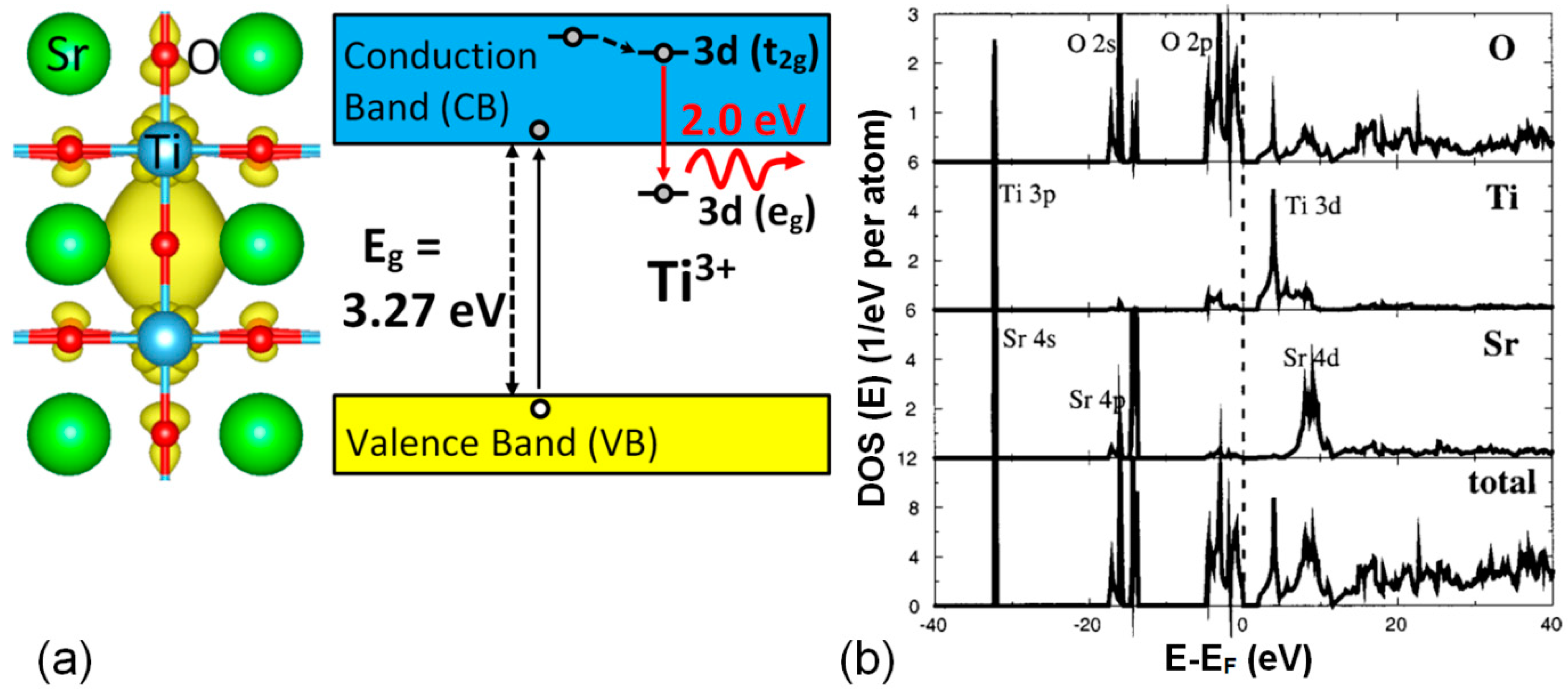
The specific model for the structure of the oxygen vacancy center has been derived from detailed theoretical DFT calculations [
12], which suggests the electronic structure schematically depicted in
Figure 8. It corresponds to a peculiar-type of F-type center, consisting of electrons trapped at host
ions adjacent to an oxygen vacancy [
9,
32], which can be designated as
. Other calculations using slightly different
ab-initio methods [
13,
14,
15] confirm this basic structure, although the results present somewhat different electronic features. In this model, the red luminescence transition at 2.0 eV (also depicted in the diagram of
Figure 9) essentially corresponds to the
optical transition between the two split states of the
electronic configuration of the
ion in octahedral symmetry. In fact, the observation of the red 2.0 eV emission in heavily strained and amorphous STO samples [
31,
42,
43], where the translational symmetry of the lattice is broken, provided key evidence that prompted the model proposed [
9].
A relevant point, which still needs to be clearly assessed, concerns the relative location of the
3d levels of the impurity within the band scheme levels of STO and, particularly, the location of the ground
3d(
eg) level in relation to the minimum of the conduction band (CBM). In relation to this point, various theoretical approaches yield different results, which depend on the charge state of the vacancy center [
15], so that it remains an open issue. As an illustrative example, theoretical calculations [
14] have yielded a value of 0.7 eV below the minimum of the conduction band (CBM). As to the location of the higher level of the 2.0 eV transition, photoemission experiments, as well as calculations, locate the Ti
3d levels at 1.5–2.5 eV above such a minimum level [
35], as illustrated in
Figure 8b. Moreover, it is clear that a realistic atomistic structure around the oxygen vacancy is a key feature for the correct analysis of the problem. This is exemplified by the anti-ferrodistortive (AFD) octahedron rotation found by Choi et al. [
65] associated with the electronic structure of the vacancy.
8. Summary and Outlook
The results and analysis presented in this review show that considerable progress has been obtained recently in the fundamental comprehension of the electronic structure of STO, including self-trapping and transport processes for electronic carriers, i.e., electrons, holes and excitons. In particular, their role on the various luminescent emissions under a variety of excitation sources, with special emphasis on experiments with laser pulses and energetic ion-beams, is now starting to be clarified. The main focus of the present review has been placed on the role of the oxygen vacancy in the stabilization of small electron-polarons and its connection with luminescence emission. It has recently been established that the electrons associated with the vacancy constitute electron-polaron states as trapped in the close vicinity of the empty oxygen site, and allow for its optical identification. A red luminescence emission centered at 2.0 eV has been unambiguously associated with polaron d–d transitions of the close to the vacancy center, as inferred from ionoluminescence (IL) experiments. These IL experiments have provided the two main requirements for the analysis and interpretation: a vacancy production mechanism through elastic ion-atom collisions and a high electronic excitation rate to induce the luminescence emission. The luminescence emission mechanisms and the light decay processes from the self-trapped excitons (STEs), are also discussed. Electrons and holes produced by irradiation very rapidly (in the sub-nanosecond time scale) form bound pairs that become self-trapped in the STO lattice. The green emission centered at 2.5 eV can be definitively attributed to the singlet-triplet transition between localized states of the STE. Recent results suggest that the blue emission at 2.8 eV, often associated with oxygen vacancies, is related to a transition from unbound conduction levels to the ground singlet state of the STE. This novel finding establishes that both the green (2.5 eV) and blue (2.8 eV) emissions result from STE transitions and rules out previous proposals assigning the 2.8 eV emission to oxygen vacancies. Results for the kinetics of those emissions can be satisfactorily discussed in terms of the simultaneous contribution of electron-hole (bimolecular) recombination processes (2.5 eV emission), together with a monomolecular recombination process for free carriers (2.8 eV). These new findings have clarified the variety of intrinsic emissions of STO and opened the path to look for similar effects in other oxide perovskites.
It is worth noting that there are several attractive routes to be carried out to achieve further progress in this field. Some complementary techniques, such as optical absorption and EPR, should be used in connection with the luminescence studies to get a further insight on the structure of the emitting centers. In relation to the STE center, it would be very useful to reach a better understanding of the detailed mechanisms of its migration and its activation energy. For the case of the oxygen vacancy, it would be relevant to conclusively assess the location of the energy levels corresponding to occupancy by one or two electrons. Moreover, it would be very useful to extend these results obtained for STO to other perovskites in order to have a more complete picture on the electronic structure and behavior of these fascinating materials, to benefit from the similarities and differences among them. These challenging questions in solid-state physics will resonate with a broad audience working on technological disciplines such as electronics, optoelectronics, photovoltaics, and photochemistry. They are, indeed, essential to design novel materials with enhanced functionalities.

 ,
, 


