Article

Modification of TiO2 Nanowire Arrays with Sn Doping as Photoanode for Highly Efficient Dye-Sensitized Solar Cells

Department of Optoelectronic Information Science, School of Materials Science and Engineering, Harbin Institute of Technology, Harbin 150001, China
*
Authors to whom correspondence should be addressed.
Submission received: 31 January 2019 / Revised: 15 February 2019 / Accepted: 16 February 2019 / Published: 21 February 2019

Abstract

:
The dye-sensitized solar cell (DSSC) is one candidate among the third-generation solar cells. The performance of most DSSCs based on TiO2 photoanode was limited by the low electron mobility within TiO2. To produce a much higher power conversion efficiency, Sn-doped TiO2 nanowire arrays were successfully prepared using a simple hydrothermal process. It was found that Sn doping augments electron mobility well and raises the flat band potential to improve the performance of DSSCs. The power conversion efficiency (η) of a DSSC based on the reasonable Sn-doped TiO2, N719 dye, platinized counter electrode and iodide/triiodide electrolyte reaches 8.75%. Furthermore, with an anatase TiO2 light scattering layer, a DSSC based on the Sn-doped TiO2 NWAs exhibits a remarkable power conversion efficiency of 9.43%, which is especially useful in weak light conditions.

Graphical Abstract

1. Introduction

Replacing the badly polluting fossil energy with environment-friendly renewable energy sources is perhaps the best way to solve the global energy crisis. As well as various clean energy sources such as hydrogen, wind, geothermal and tidal energy, solar energy seems to be a good candidate to be the next generation energy source because the irradiation energy provided by the sun to the surface of the earth exceeds global energy consumption. Methods for converting solar energy into usable energy is therefore the most important research and development issue for researchers.
A solar cell based on photovoltaic (PV) technology is a way to convert solar energy into directly available electric energy [1,2]. Since the silicon-based solar cell was first designed [3], solar cells have been developing over several stages. Nevertheless, the application of the silicon-based solar cells (single or multi crystalline) is limited by complex preparation methods and high manufacturing costs. The remarkable invention of the dye-sensitized solar cell (DSSC) by Grätzel and his cooperators [4]—a photoelectrochemical cell—has drawn much attention due to low manufacturing cost, simple manufacturing process and being environmentally friendly [5]. Over the past two decades, the power conversion efficiency of the dye-sensitized solar cell has been low compared with the silicon-based solar cell, but the DSSC is still a considerable candidate for producing a much higher power conversion efficiency at a later time [6,7,8,9,10,11].
As a rule, DSSC is a sandwich structure composed of a photoanode covered with a monolayer of dye molecules on a semiconductor surface, electrolytes and a counter electrode [12]. Much endeavor has been focused on the design or modification of the novel dyes [13], the novel types of electrolyte [14] or counter electrodes [15]. The photoanode also plays a key role in the operation of the DSSC, therefore, it is crucial to develop new photoanodes to improve the power conversion efficiency of DSSC.
Numerous semiconductor materials have been investigated for use as photoanodes in DSSCs, such as TiO2 [16], ZnO [17], SnO2 [18], In2O3 [19]. Among these semiconductor materials, most researchers employed TiO2 nanomaterials as the photoanode of DSSCs owing to its excellent physical and chemical properties such as having a suitable isoelectric point for dye absorption, proper energy band structure for charge injection from dye molecules, well passivity to photo corrosion [20,21,22,23], and appropriate electronic orbit for reducing probability of photogenerated charges recombination [24]. In a general way, tetragonal anatase and rutile TiO2 are commonly applied in DSSCs, and rutile is the most stable crystalline phase of TiO2. The relatively lower electron mobility of rutile TiO2 leads to larger density of states near the conduction band minimum, which could provide additional efficient electron transfer channels to render much faster electron transfer in DSSCs based on rutile TiO2 [25].
The photoanode needs the highest possible specific surface area for dye adsorption, a porous structure for complete electrolyte immersion and a fast charge mobility rate to minimize photogenerated charges loss [26]. In early research, TiO2 nanoparticles (NPs) were usually used as the photoanode of DSSCs [4]. NPs can provide a very large surface area for dye adsorption due to large specific surface area, electron traps caused by massive amounts of grain boundaries still limit the further improvement of the performance of DSSCs [27,28,29,30,31,32]. Extensive efforts to overcome this disadvantage have been focused on the preparation of single-crystal one-dimensional (1D) nanostructures such as nanorods (NRs), nanowires (NWs), nanotubes (NTs) and nanobelts (NBs) [33,34,35,36]. Compared with NPs film, single-crystal 1D nanostructures could provide direct carrier transport pathways to the external circle, which would increase the charge carrier collection. There are fewer defects in single-crystal 1D nanostructures of high crystallization quality, which decrease the recombination of the photogenerated carriers in the photoanode [37,38]. Among these nanostructures, rutile TiO2 nanowire arrays (NWAs) are considered because they maintain the advantages of one-dimensional nanomaterials, while the large specific surface area can load more dye molecules.
Low electron mobility hampers the application of rutile TiO2 NWAs in DSSCs. Doping elements is a practical method for optimizing the TiO2 NWAs. Doping elements could shift the flat-band potential, decrease the recombination rate of photogenerated carriers and increase the speed of electron transport, but the choice of doping elements is predominant for the performance of DSSCs. Various elements of doped TiO2 nanostructures have been studied in DSSCs such as V [39,40], Cr [41,42], Mn [43], Fe [44], Cu [45], Zn [46,47,48,49,50,51,52]. However, DSSCs based on Sn-doped TiO2 NWAs photoanodes have not been studied. Stannum (Sn) is a candidate for doping into the crystal lattice of rutile TiO2. The crystal structure and lattice constant of Tin dioxide (SnO2) are close to those of rutile TiO2, so the doping would not introduce defects that would trap the photogenerated electrons. The electron mobility and band gap of SnO2 is 100~200 cm2 V−1 s−1 [53] and 3.8 eV, respectively, which are higher than those of rutile TiO2 (0.1–1 cm2 V−1 s−1 [54], 3.0 eV). It could be expected that doping Sn into rutile TiO2 NWAs could well augment the electron mobility, thus decreasing the recombination possibility of photogenerated electrons at the interface of photoanode and electrolyte [55] Compared with TiO2, the lower isoelectric point of SnO2 limited the loading of acidic carboxyl dye molecules [56]. So, finding a suitable doping ratio of Sn is a crucial work.
In this paper, we prepared Sn-doped TiO2 NWAs using a simple hydrothermal process and then assembled DSSCs based on these photoanodes with N719 dye, platinized counter electrode and iodide/triiodide electrolyte. It was found that Sn doping augments electron mobility well and raises the flat band potential to improve the performance of DSSC. Furthermore, with an anatase TiO2 light scattering layer, DSSC based on the Sn-doped TiO2 NWAs exhibits a remarkable power conversion efficiency of 9.43%.

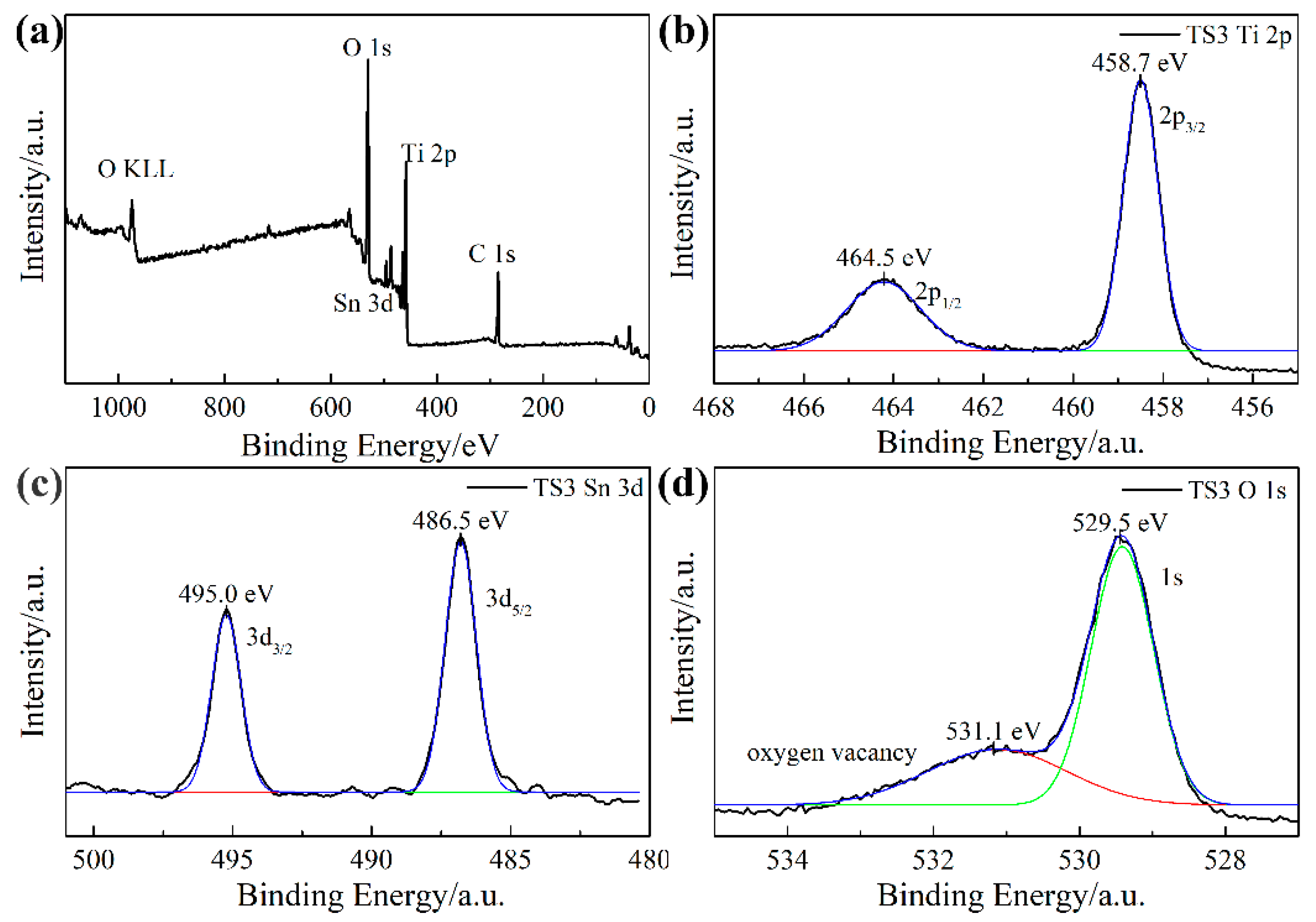
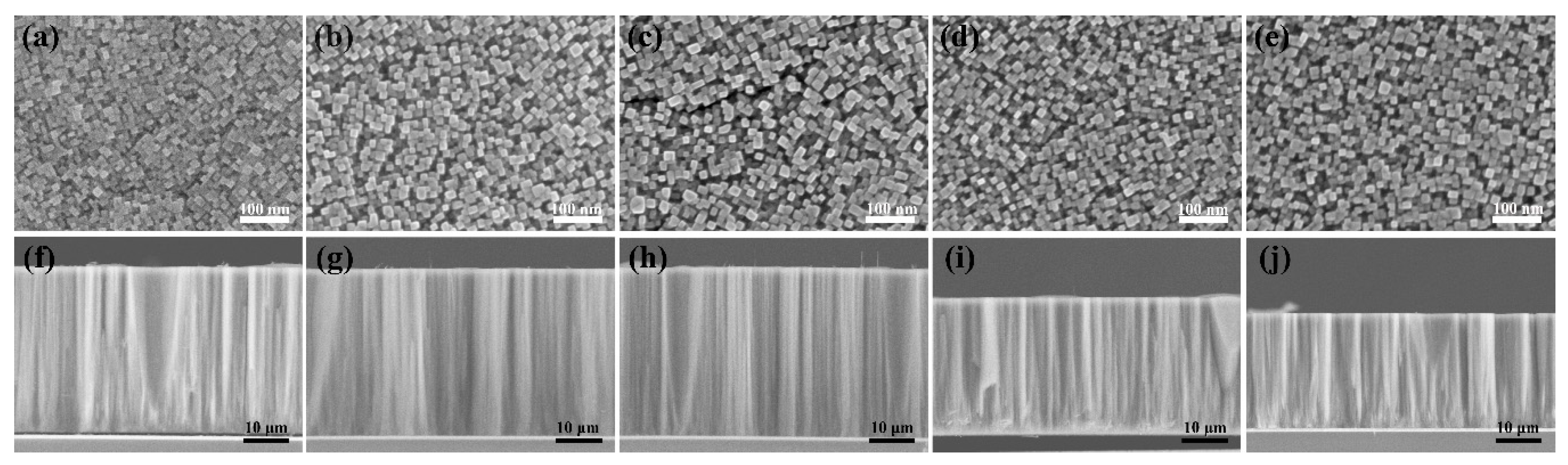
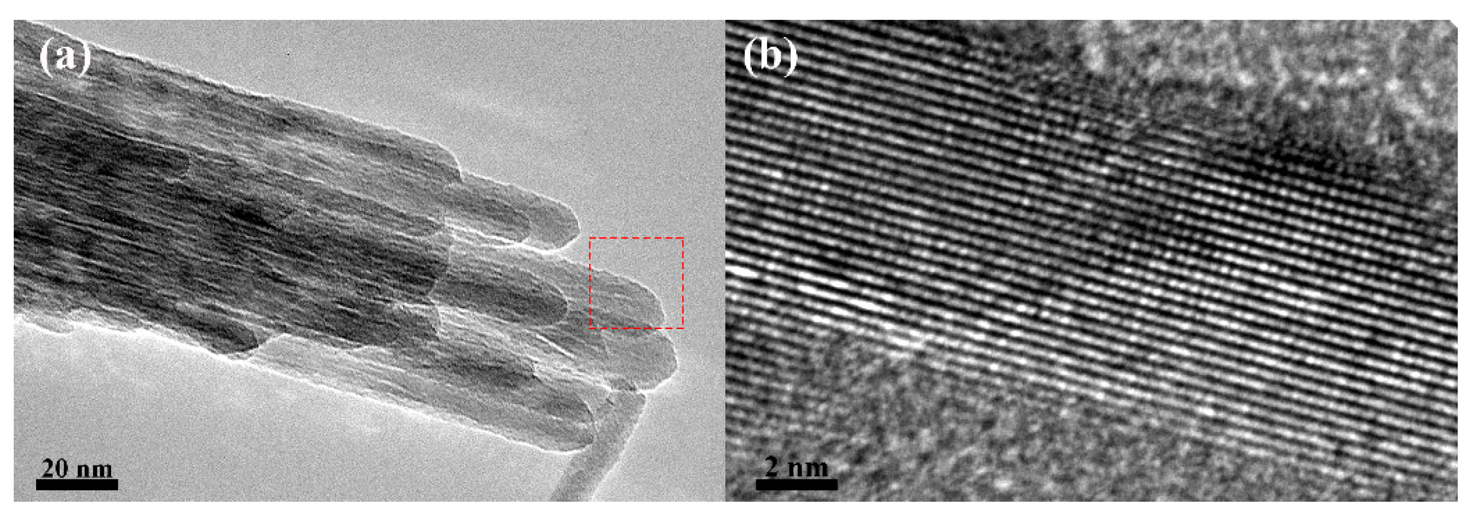
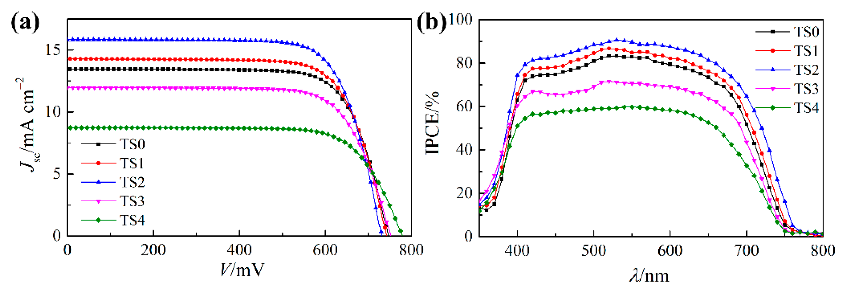
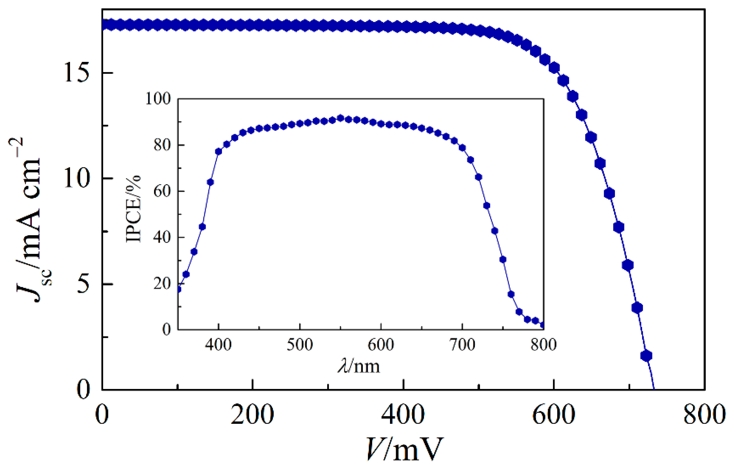
2. Results and Discussion

The preparation of pure TiO2 NWAs (TS0) and Sn-doped TiO2 NWAs (TS1, TS2, TS3, TS4) is shown in the Supplementary Materials. First, we used inductively coupled plasma optical emission spectrometry to measure the ratio of Sn/Ti. With SnCl4 increasing in reaction resolution, the ratio of Sn/Ti is about 5/95, 11/89, 15/85 and 21/79, respectively, consistent with the reaction resolution.
The crystalline structure and the lattice parameters were examined using X-ray diffraction (XRD, PANalytical B.V., Almelo, Holland) in the 2θ range of 30°~80°. XRD patterns of pure TiO2 NWAs (TS0) and Sn-doped TiO2 NWAs (TS1, TS2, TS3, TS4) are shown in Figure 1a. The only diffraction peak of TS0 was located at 62.72° which could be indexed to the rutile phase TiO2 (JCPDS 21-1276) and the small half-peak width indicated single growth orientation and high crystallization quality. The (002) plane suggests that [001] orientation is the crystal preferential orientation of the hydrothermal method to prepare TiO2 NWAs. No extra peaks could be explained by the uniformity of the Sn doping and the formation of the uniform solid solution. As the XRD pattern of the (002) peak was enlarged, it was noted that with the amount of Sn doping increasing, the position of the diffraction peak of TS1, TS2, TS3 and TS4 moved to a smaller angle, as shown in Figure 1b. The shift of the position of the diffraction peak means the augment of lattice parameters, which may be related to that the ionic radii of Ti ions (0.061 nm), is smaller than that of Sn ions (0.071 nm) [57].
Raman spectroscopy (HORIBA Jobin Yvon, Pairs, France) was employed to further analyze the spatial uniformity and variation of bonds to characterize the effect of the Sn-doping in the TiO2 NWs. Figure 2a shows the Raman spectra of samples TS0, TS1, TS2, TS3 and TS4 in the range of 100–800 cm−1. For the pure rutile TiO2 (sample TS0), four typical vibrational modes were perceived for rutile TiO2 around 145 cm−1 (B1g), 445 cm−1 (Eg), 610 cm−1 (A1g), and 240 cm−1 for second-order effect (SOE) [58,59,60]. No peaks related to SnO2 were detected, also indicating the uniformity of the Sn doping and the formation of the uniform solid solution. These typical vibrational modes were comprised of Ti-O bonds and the variation of lattice parameters resulted in the opposite moving of the O atoms in the adjacent O-Ti-O bonds [61]. Apparently, their positions moved to a lower wavenumber as the contents of Sn increased. As shown in Figure 2b, the red-shift of the B1g, Eg and A1g mode of samples TS1, TS2, TS3, TS4 suggested the more internal strains were caused by Sn-doping in the NWs and a smaller Hooke constant, indicating weaker Ti-O bond involvement and larger lattice parameters, consistent with the XRD results.
In order investigate the Sn-doped TiO2 NWAs—a substitutional solid solution or interstitial solid solution—X-ray photoelectron spectroscopy (XPS, Thermo Fisher Scientific, Waltham, MA, USA) was used to analyze the bonding state of samples TS2. For the pure rutile TiO2, the two characteristic peaks of the Ti 2p spectrum were located at 464.4 eV and 458.6 eV, which are related to Ti 2p1/2 and 2p3/2, respectively [62,63]. For the pure rutile SnO2, the two characteristic peaks of the Sn 3d spectrum were located at 495.4 eV and 486.9 eV, which are related to 3d3/2 and 3d5/2, respectively [64,65]. As shown in Figure 3a, the fully scanned XPS spectra confirmed that the existence of Ti, Sn, and O were detected in the nanowire. As shown in Figure 3b, the peak positions of two detected peaks in the spectrum of the Ti 2p showed a small positive shift of 0.1 eV toward higher binding energy compared to the pure rutile TiO2. Meanwhile, the peak positions of the two detected peaks in the spectrum of the Sn 3d showed a small negative shift of 0.4 eV toward lower binding energy compared to the pure rutile TiO2, as shown in Figure 3c. Considering that the electronegativity of Ti (1.54) is a little smaller than that of Sn (1.96) vs, the small shift of binding energy is ascribed to the presence of Sn metallic ions in TiO2 lattice bringing about parts of electrons deviating from the Ti metallic ions [66,67,68,69]. The small shift of binding energy also confirms that the Sn replaces the Ti in the TiO2 lattice but does not embed in the lattice gap. In other words, the Sn doping is also uniform at the atomic level, which was consistent with the XRD and Raman results. The O 1s spectrum of Sample TS3 can be deconvoluted to two peaks, as shown in Figure 3d. The binding energy of O-Ti is 529.36 eV, and the binding energy of O-Sn is about 530.8 eV. One peak of the O 1s spectrum located at 529.5 eV, which suggests the formation of a Sn-O-Ti linkage in the nanowire [70]. The peak located at 531.1 eV is assigned to oxygen vacancy and the surface-adsorbed H2O [71,72,73].
The microstructure and microtopography are of great significance for the performance of nanomaterials. The morphology of pure TiO2 NWAs (TS0) and Sn-doped TiO2 NWAs (TS1, T32, TS3, TS4) were examined using the field emission scanning electron microscopy (FESEM, JEOL, Akishima-shi, Tokyo, Japan). Figure 4a–e are the top-surface images of different samples, in which we can clearly observe highly uniform and ordered nanowires with square cross sections. The average square edge length of each nanowire is approximately 15 nm which means that the concentration of Sn in the reaction solution does not affect the cross sections of all samples. Figure 4f–j show cross-sectional images of different samples, indicating that the growth of nanowires is almost perpendicular to the FTO substrates. This result is consistent with the XRD result. Obviously, the thickness of the NWAs is affected by the concentration of Sn in the reaction solution. While the concentration of Sn in the reaction solution is low, the thicknesses of TS1 and TS2 are nearly the same as that of the pure TiO2 NWAs (TS0, 30 μm); however, with the concentration of Sn in the reaction solution increasing, for TS3 and TS4, the thickness decreases to 26 and 20 μm, respectively. As we know, the deposition and dissolution of NWs are processes of dynamic equilibrium. Because the SnO2 is more easily eroded by HCl, as the concentration of Sn in the reaction solution increases, the dissolution of NWs aggravates, leading to less thickness. Figures S1 and S2 depict the element-mapping characterization of the top-surface area and the cross section of the Sn-doped TiO2 NWAs (TS2), indicating that Sn is homogeneously distributed in TiO2 NWAs.
Transmission electron microscopy (TEM, JEOL, Akishima-shi, Tokyo, Japan) and high-resolution TEM (HRTEM, JEOL Akishima-shi, Tokyo, Japan) were used to examine more detailed data about the microstructures of the Sn-doped TiO2 NWAs (sample TS2). As shown in Figure 5a, the structure of the Sn-doped TiO2 NWAs is porous, which helps dye loading and electrolyte penetration which is beneficial for the improvement of DSSCs. The clear lattice fringes can be found in the HRTEM image, as shown in Figure 5b. The ∼0.342 nm interplanar spacing of the Sn-doped TiO2 NWAs is a little more than that of pure TiO2 NWAs, suggesting the formation of the Sn-doped TiO2 NWAs, consistent with above results. The distribution of Sn in nanowires (sample TS2) was investigated by TEM with an electron energy loss spectrometer (EELS). As shown in Figure S3, EELS elemental mappings also indicate that the Sn is uniformly distributed among entire TiO2 NWs, indicating the formation of Sn doped TiO2 NWAs.
The pure TiO2 nanowire arrays and Sn-doped TiO2 nanowire arrays with N719 dye platinized counter electrode and iodide/triiodide electrolyte were employed as photoanodes to prepare the DSSCs. The detailed methods are shown in the Supplementary Materials. Figure 6a shows the typical current density (J)−voltage (V) curves of the as-prepared DSSCs based on the pure TiO2 NWAs and Sn-doped TiO2 NWAs under simulated AM1.5G sunlight with 100 mW cm‒2, and the corresponding detailed DSSC parameters are listed in Table 1. The short-circuit photocurrent density (Jsc), open-circuit voltage (Voc), fill factor (FF) and power conversion efficiency (η) of the DSSC based on the pure TiO2 NWAs (TS0) are 13.46 mA cm‒2, 748 mV, 0.741 and 7.46%, respectively. For DSSCs based on the Sn-doped TiO2 NWAs (TS1, TS2, TS3, TS4) with an increasing doping amount of Sn, the Jsc augments from 14.28 to 15.84 mA cm‒2 and then decreases to 8.73 mA cm‒2; meanwhile, the Voc gradually increased. The increased Voc is related to higher flat-band potentials, as shown in Figure S4 [74]. A maximum η of 8.72% was obtained for the DSSC based on TS2 Sn-doped TiO2 NWAs photoanode, which may be mostly attributed to the largest Jsc.
To seek the cause of the Jsc changes, the incident photon-to-current conversion efficiency (IPCE) spectra of DSSCs based on the pure TiO2 NWAs and Sn-doped TiO2 NWAs was tested in the range of 350~800 nm. As shown in Figure 6b, the change trend of IPCE is consistent with that of Jsc of DSSCs. The IPCE of the DSSC with TS2 is higher than that of DSSC with other photoanodes (TS0, TS1, TS3) over the spectra ranging from 400~800 nm. Nevertheless, the IPCE enhanced with the increasing Sn amount over the spectra ranging from 350~400 nm. For the TS3 and TS4, the lower IPCE may be due to the smaller thickness which could not load enough dye molecule and higher flat-band potentials may inhibit injection of photoelectrons [74].
Compared with the DSSC based on pure TiO2 NWAs, the enhancement in the IPCE for the DSSCs based on Sn-doped TiO2 NWAs may be attributed to the light harvesting ability and photogenerated electron recombination at the interface of photoanode and electrolyte [75].
The light harvesting ability is related to the dye-uptake amounts and the light trapping by the photoanode. For the pure TiO2 NWAs and Sn-doped TiO2 NWAs, the dye-uptake amounts decreased from 390.4 to 288.6 nmol cm‒2 as the doping amount of Sn increased, as shown in Table 1. The dye-uptake amount is relevant to the isoelectric points of photoanode. Considering the lower isoelectric point (IEP) of SnO2 is lower than that of TiO2 [76], the decrease of the dye-uptake amounts could be understood. As shown in Figure S5, compared to the isoelectric point of the pure TiO2 NWAs, the presence of Sn in TiO2 NWAs decreases the isoelectric point from 6.4 to 5.8, which would inhibit the attachment of dye molecules with acidic carboxyl groups [77]. The smaller thickness would also decrease the dye-uptake amounts.
To make certain the effect of the doping amount of Sn on the light trapping by the photoanode, UV-vis diffuse reflectance spectra measurement was carried out. The thickness of NWAs is so large that no light could pass through the nanowire arrays, in other words, the less reflection indicates more absorption. As shown in Figure S6a, the variation in the reflection of the pure TiO2 NWAs (TS0) and Sn-doped TiO2 NWAs (TS1, TS2, TS3) is regular. With the doping amount of Sn increasing, the absorption of samples is enhanced at a range of wavelengths from 300 to 400 nm. This result is consistent with the IPCE result. The reflection rate was normalized, as shown in Figure S6b, indicating absorbing edge blue shifting. The equation for calculating the optical forbidden bandwidth from the diffuse reflectance is shown in the supplementary information. As shown in Figure S6c, the optical forbidden bandwidth of samples (TS0, TS1, TS2, TS3) with the doping amount of Sn is estimated to be 2.97, 3.00, 3.01 and 3.02, respectively. The larger band gap is beneficial to increasing the light absorption range of DSSCs.
To make clear the effect of the Sn doping in TiO2 NWAs on photogenerated electron recombination at the interface of photoanode and electrolyte, we measured the dark current of DSSCs based on the pure TiO2 NWAs (TS0) and Sn-doped TiO2 NWAs (TS1, TS2, TS3, TS4). As shown in Figure S7, the Sn could reduce the dark current of the DSSCs at a given potential, indicating that Sn doping in TiO2 NWAs can inhibit the photogenerated electron recombination at the interface of the photoanode and electrolyte. The lower dark current is related to higher Voc, which is consistent with the above results [78].
To understand how to affect the photogenerated electron recombination at the interface of the photoanode and electrolyte, the photoluminescence (PL) spectrum was used to test the separation of photogenerated electron–hole pairs [79]. Figure 7a shows the PL spectra of the pure TiO2 NWAs (TS0) and Sn-doped TiO2 NWAs (TS1, TS2, TS3, TS4). It is noted that the intensity of PL peaks notably decreases as the doping amount of Sn increases, indicating that Sn doping could accelerate the separation of photogenerated electron–hole pairs. This may be due to the Sn doping enhancing the electron mobility of TiO2 NWAs. To further analyze charge transfer kinetics in these DSSCs, electrochemical impedance spectroscopy (EIS) is carried out under 750 mV bias in dark conditions, as shown in the inset of Figure S8. All obtained curves show two arcs in low frequency and middle frequency regions. According to previous research, the enlarged low-frequency arc implies the charge transfer resistance of the photoanode, as shown in Figure S8 [80]. Through the fitting with Z-view, the resistance of the electrode could be calculated as shown in Table S1. As the doping amount of Sn increases, the charge transfer resistance gradually decreases, which certifies that the Sn doping can effectively improve charge transfer performance. We further utilized the transient photoelectric decay technique to find out the effect of the electron lifetime (τtpd) on the doping amount of Sn in the DSSCs based on the pure TiO2 NWAs (TS0) and Sn-doped TiO2 NWAs (TS1, TS2, TS3, TS4). As displayed in Figure 7b, the τtpd in DSSCs based on the Sn-doped TiO2 (TS1, TS2, TS3, TS4) are non-negligibly higher than that of DSSC based on the pure TiO2 NWAs (TS0) at a certain extracted charge. With the doping amount of Sn increasing, the τtpd augments, which is identical to the variation trend of the dark current. Consistent with the PL results, the higher τtpd is mainly due to the Sn doping enhancing electron mobility [81,82,83], manifesting the noticeable suppression of the photogenerated electron recombination at the interface of the photoanode and electrolyte which contributes to higher IPCE and Jsc as well as Voc.
Additional light scattering layer on the photoanode could effectively improve the performance of DSSC [80]. An anatase TiO2 particles (WERO-4, Dyesol) layer with 5 μm thickness was used as a light scattering layer on the Sn-doped TiO2 NWAs (TS2) by stencil printing, which was applied as a photoanode to prepared DSSC. As displayed in Figure 8, under a simulated AM1.5G sunlight irradiance of 100 mW cm−2, as-prepared DSSC shows a remarkable η of 9.26% with Jsc of 17.28 mA cm−2, Voc of 735 mV, and FF of 0.729 which is a considerably high-power conversion efficiency for DSSCs. Moreover, the inset of Figure 8 showed the IPCE spectrum of this DSSC. The enhancement of IPCE is attributed to the efficient light harvesting due to the light-scattering layer of larger particles [84]. The power conversion efficiency of weak light also attracted the attention of researchers [85], so we measured the DSSC parameters under irradiation with different light intensities, and detailed data are listed in Table 2. Under an irradiation with 20.29 mW cm‒2 light intensity, this DSSC reaches a remarkable power conversion efficiency of 9.43%.

3. Conclusions

We have successfully produced Sn-doped TiO2 NWAs using simple hydrothermal methods and have analyzed their performance as a photoanode in DSSCs. The prepared Sn-doped is 30 μm length with a Square section of 15 nm average square edge length. XRD, Raman and XPS results confirmed the success of Sn doping. It is found that Sn doping augments electron mobility well and raises the flat band potential to improve the performance of DSSC. The power conversion efficiency (η) of DSSC based on the reasonable Sn-doped TiO2, N719 dye, platinized counter electrode and iodide/triiodide electrolyte reaches 8.75%. Furthermore, with an anatase TiO2 light scattering layer, DSSC based on the Sn-doped TiO2 NWAs exhibits a remarkable power conversion efficiency of 9.43%, especially useful in the weak light conditions.

Supplementary Materials

The following are available online at https://0-www-mdpi-com.brum.beds.ac.uk/2073-4352/9/2/113/s1, Experimental method, Figure S1: EDS elemental mapping images of cross section of Sn-doped TiO2 NWAs (TS2), Figure S2: EDS elemental mapping images of top surface of Sn-doped TiO2 NWAs (TS2), Figure S3: (a) the tip region of Sn-doped TiO2 NWAs (TS2). Corresponding EELS elemental mapping images for b) Sn, c) Ti, and d) O, respectively, Figure S4: Mott-Schottky plots of the pure TiO2 NWAs (TS0) and Sn-doped TiO2 NWAs (TS1, TS2, TS3, TS4), Figure S5: The pH-dependent zeta-potential of the pure TiO2 NWAs (TS0) and Sn-doped TiO2 NWAs (TS1, TS2, TS3, TS4)., Figure S6: (a) The UV-vis diffusive reflectance spectra of the pure TiO2 NWAs (TS0) and Sn-doped TiO2 NWAs (TS1, TS2, TS3), (b) normalized UV-vis diffusive reflectance spectra and (c) the plots of transforming the Kubelka–Munk function versus the energy of light, Figure S7: Dark current density–voltage of DSSCs based on the pure TiO2 NWAs (TS0) and Sn-doped TiO2 NWAs (TS1, TS2, TS3, TS4); Figure S8: The enlarged low-frequency arc and full scale (inset graph) Nyquist plots of the DSSCs based on the pure TiO2 NWAs (TS0) and Sn-doped TiO2 NWAs (TS1, TS2, TS3, TS4) measured under 750 mV bias in the dark condition; Table S1: Detailed simulative values of the charge transfer resistance from EIS spectra.

Author Contributions

F.G. and D.W. designed the experiments; S.N. and B.W. performed the experiments; S.N., Y.Z., J.W. and S.J. analyzed the data; Y.Z., J.W. and S.J. contributed analysis tools; S.N. and D.W. wrote the paper, L.Z. coordinated the overall work.

Funding

This research was funded by the National Natural Science Foundation of China (Grant No. 51502061) and (Grant No. 61605036).

Conflicts of Interest

The authors declare no conflict of interest.

References

  1. Goetzberger, A.; Hebling, C.; Schock, H.W. Photovoltaic Materials, History, Status and Outlook. Mater. Sci. Eng. R 2003, 40, 1–46. [Google Scholar] [CrossRef]
  2. Polman, A.; Knight, M.; Garnett, E.C.; Ehrler, B.; Sinke, W.C. Photovoltaic Materials: Present Efficiencies and Future Challenges. Science 2016, 352, aad4424. [Google Scholar] [CrossRef]
  3. Chapin, D.M.; Fuller, C.S.; Pearson, G.L. A New Silicon p-n Junction Photocell for Converting Solar Radiation into Electrical Power. J. Appl. Phys. 1954, 25, 676–677. [Google Scholar] [CrossRef]
  4. O’Regan, B.; Grätzel, M. A Low-cost, High-efficiency Solar Cell Based on Dye-sensitized Colloidal TiO2 Films. Nature 1991, 353, 737–740. [Google Scholar] [CrossRef]
  5. Fakharuddin, A.; Jose, R.; Brown, T.M.; Fabregat-Santiago, F.; Bisquert, J. A Perspective on the Production of Dye-sensitized Solar Modules. Energy Environ. Sci. 2014, 7, 3952. [Google Scholar] [CrossRef]
  6. Hagfeldt, A.; Boschloo, G.; Sun, L.; Kloo, L.; Pettersson, H. Dye-sensitized Solar Cells. Chem. Rev. 2010, 110, 6595–6663. [Google Scholar] [CrossRef]
  7. Snaith, H.J.; Schmidt-Mende, L. Advances in Liquid-electrolyte and Solid-state Dye-sensitized Solar Cells. Adv. Mater. 2007, 19, 3187–3200. [Google Scholar] [CrossRef]
  8. Cuce, E.; Young, C.-H.; Riffat, S.B. Thermal performance investigation of heat insulation solar glass: A comparative experimental study. Energy Build. 2015, 86, 595–600. [Google Scholar] [CrossRef]
  9. Cuce, E.; Riffat, S.B.; Young, C.-H. Thermal insulation, power generation, lighting and energy saving performance of heat insulation solar glass as a curtain wall application in Taiwan: A comparative experimental study. Energ. Convers. Manag. 2015, 96, 31–38. [Google Scholar] [CrossRef]
  10. Kong, L.; Liu, G.; Gong, J.; Hu, Q.; Dera, P.; Zhang, D.; Liu, Z.; Yang, W.; Zhu, K.; Tang, Y.; et al. Simultaneous band-gap narrowing and carrier-lifetime prolongation of organic-inorganic trihalide perovskites. Proc. Natl. Acad. Sci. USA 2016, 113, 8910–8915. [Google Scholar] [CrossRef]
  11. Nogueira, A.F.; Longo, C.; De Paoli, M.-A. Polymers in dye sensitized solar cells: Overview and perspectives. Coord. Chem. Rev. 2004, 248, 1455–1468. [Google Scholar] [CrossRef]
  12. Huang, Y.; Wu, H.; Yu, Q.; Wang, J.; Yu, C.; Wang, J.; Gao, S.; Jiao, S.; Zhang, X.; Wang, P. Single-Layer TiO2 Film Composed of Mesoporous Spheres for High-Efficiency and Stable Dye-Sensitized Solar Cells. ACS Sustain. Chem. Eng. 2018, 6, 3411–3418. [Google Scholar] [CrossRef]
  13. Yu, Q.; Zhou, D.; Shi, Y.; Si, X.; Wang, Y.; Wang, P. Stable and efficient dye-sensitized solar cells: Photophysical and electrical characterizations. Energy Environ. Sci. 2010, 3, 1722–1725. [Google Scholar] [CrossRef]
  14. Zhou, D.; Yu, Q.; Cai, N.; Bai, Y.; Wang, Y.; Wang, P. Efficient organic dye-sensitized thin-film solar cells based on the tris(1,10-phenanthroline) cobalt (II/III) redox shuttle. Energy Environ. Sci. 2011, 4, 2030–2034. [Google Scholar] [CrossRef]
  15. He, B.; Meng, X.; Tang, Q. Low-Cost Counter Electrodes From CoPt Alloys For Efficient DyeSensitized Solar Cells. ACS Appl. Mater. Interfaces 2014, 6, 4812–4818. [Google Scholar] [CrossRef]
  16. Yun, J.H.; Wang, L.; Amal, R.; Ng, Y.H. One-Dimensional TiO2 Nanostructured Photoanodes: From Dye-Sensitised Solar Cells to Perovskite Solar Cells. Energies 2016, 9, 1030. [Google Scholar] [CrossRef]
  17. Zhang, Q.; Dandeneau, C.S.; Zhou, X.; Cao, G. ZnO Nanostructures for Dye-Sensitized Solar Cells. Adv. Mater. 2009, 21, 4087–4108. [Google Scholar] [CrossRef]
  18. Fukai, Y.; Kondo, Y.; Mori, S.; Suzuki, E. Highly Efficient Dye-Sensitized SnO2 Solar Cells Having Sufficient Electron Diffusion Length. Electrochem. Commun. 2007, 9, 1439–1443. [Google Scholar] [CrossRef]
  19. Mahalingam, S.; Abdullah, H. Electron Transport Study of Indium Oxide as Photoanode in DSSCs: A Review. Renew. Sustain. Energy Rev. 2016, 63, 245–255. [Google Scholar] [CrossRef]
  20. Wang, X.; Li, Z.; Shi, J.; Yu, Y. One-Dimensional Titanium Dioxide Nanomaterials: Nanowires, Nanorods, and Nanobelts. Chem. Rev. 2014, 114, 9346–9384. [Google Scholar] [CrossRef]
  21. Leung, D.; Fu, X.; Wang, C.; Ni, M.; Leung, M.; Wang, X.; Fu, X. Hydrogen Production over Titania-Based Photocatalysts. ChemSusChem 2010, 3, 681–694. [Google Scholar] [CrossRef] [PubMed]
  22. Liu, G.; Kong, L.; Guo, P.; Stoumpos, C.C.; Hu, Q.; Liu, Z.; Cai, Z.; Gosztola, D.J.; Mao, H.; Kanatzidis, M.G.; et al. Two Regimes of Bandgap Red Shift and Partial Ambient Retention in Pressure-Treated Two-Dimensional Perovskites. ACS Energy Lett. 2017, 2, 2518–2524. [Google Scholar] [CrossRef]
  23. Liu, G.; Gong, J.; Kong, L.; Schaller, R.D.; Hu, Q.; Liu, Z.; Yan, S.; Yang, W.; Stoumpos, C.C.; Kanatzidis, M.G.; et al. Isothermal pressure-derived metastable states in 2D hybrid perovskites showing enduring bandgap narrowing. Proc. Natl. Acad. Sci. USA 2018, 115, 8076–8081. [Google Scholar] [CrossRef] [PubMed]
  24. Jose, R.; Thavasi, V.; Ramakrishna, S. Metal oxides for dye-sensitized solar cells. J. Am. Ceram. Soc. 2009, 92, 289–301. [Google Scholar] [CrossRef]
  25. Wei, H.; Luo, J.; Li, S.; Wang, L. Revealing the Origin of Fast Electron Transfer in TiO2-based Dye-Sensitized Solar Cells. J. Am. Chem. Soc. 2016, 138, 8165–8174. [Google Scholar] [CrossRef] [PubMed]
  26. Roslan, N.; Ya’acob, M.E.; Radzi, M.A.M.; Hashimoto, Y.; Jamaludin, D.; Chen, G. Dye Sensitized Solar Cell (DSSC) greenhouse shading: New insights for solar radiation manipulation. Renew. Sustain. Energy Rev. 2018, 92, 171–186. [Google Scholar] [CrossRef]
  27. Oekermann, T.; Zhang, D.; Yoshida, T.; Minoura, H. Electron Transport and Back Reaction in Nanocrystalline TiO2 Films Prepared by Hydrothermal Crystallization. J. Phys. Chem. B 2004, 108, 2227–2235. [Google Scholar] [CrossRef]
  28. Villanueva-Cab, J.; Wang, H.; Oskam, G.; Peter, L.M. Electron Diffusion and Back Reaction in Dye-Sensitized Solar Cells: The Effect of Nonlinear Recombination Kinetics. J. Phys. Chem. Lett. 2010, 1, 748–751. [Google Scholar] [CrossRef] [Green Version]
  29. Fisher, A.C.; Peter, L.M.; Ponomarev, E.A.; Walker, A.B.; Wijayantha, K.G.U. Intensity Dependence of the Back Reaction and Transport of Electrons in Dye-Sensitized Nanocrystalline TiO2 Solar Cells. J. Phys. Chem. B 2000, 104, 949–958. [Google Scholar] [CrossRef]
  30. Nelson, J. Continuous-time random-walk model of electron transport in nanocrystalline TiO2 electrodes. Phys. Rev. B 1999, 59, 15374. [Google Scholar] [CrossRef]
  31. Kang, S.H.; Choi, S.H.; Kang, M.S.; Kim, J.Y.; Kim, H.S.; Hyeon, T.; Sung, Y.E. Nanorod-Based Dye-Sensitized Solar Cells with Improved Charge Collection Efficiency. Adv. Mater. 2008, 20, 54–58. [Google Scholar] [CrossRef] [Green Version]
  32. Lee, B.H.; Song, M.Y.; Jang, S.-Y.; Jo, S.M.; Kwak, S.-Y.; Kim, D.Y. Charge Transport Characteristics of High Efficiency Dye-Sensitized Solar Cells Based on Electrospun TiO2 Nanorod Photoelectrodes. J. Phys. Chem. C 2009, 113, 21453–21457. [Google Scholar] [CrossRef]
  33. Zhou, Z.J.; Fan, J.Q.; Wang, X.; Zhou, W.H.; Du, Z.L.; Wu, S.X. Effect of Highly Ordered Single-Crystalline TiO2 Nanowire Length on the Photovoltaic Performance of Dye-Sensitized Solar Cells. ACS Appl. Mater. Interfaces 2011, 3, 4349–4353. [Google Scholar] [CrossRef] [PubMed]
  34. Yang, L.; Leung, W.W. Application of a Bilayer TiO2 Nanofiber Photoanode for Optimization of Dye-Sensitized Solar Cells. Adv. Mater. 2011, 23, 4559–4562. [Google Scholar] [CrossRef] [PubMed]
  35. Wang, Z.; Wang, H.; Liu, B.; Qiu, W.; Zhang, J.; Ran, S.; Huang, H.; Xu, J.; Han, H.; Chen, D.; et al. Transferable and Flexible Nanorod-Assembled TiO2 Cloths for Dye-Sensitized Solar Cells, Photodetectors, and Photocatalysts. ACS Nano 2011, 5, 8412–8419. [Google Scholar] [CrossRef] [PubMed]
  36. Sun, P.; Zhang, X.; Liu, X.; Wang, L.; Wang, C.; Yang, J.; Liu, Y. Growth of Single-Crystalline Rutile TiO2 Nanowire Array on Titanate Nanosheet Film for Dye-Sensitized Solar Cells. J. Mater. Chem. 2012, 22, 6389–6393. [Google Scholar] [CrossRef]
  37. Xie, J.L.; Guo, C.X.; Li, C.M. Construction of One-Dimensional Nanostructures on Graphene for Efficient Energy Conversion and Storage. Energy Environ. Sci. 2014, 7, 2559–2579. [Google Scholar] [CrossRef]
  38. Weng, B.; Liu, S.; Tang, Z.-R.; Xu, Y.-J. One-Dimensional Nanostructure Based Materials for Versatile Photocatalytic Applications. RSC Adv. 2014, 4, 12685–12700. [Google Scholar] [CrossRef]
  39. Liu, Z.; Li, Y.; Liu, C.; Ya, J.; Lei, E.; Zhao, W.; Zhao, D.; An, L. TiO2 Photoanode Structure with Gradations in V Concentration for Dye-Sensitized Solar Cells. ACS Appl. Mater. Interfaces 2011, 3, 1721–1725. [Google Scholar] [CrossRef]
  40. Liu, J.; Duan, Y.; Zhou, X.; Lin, Y. Influence of VB Group Doped TiO2 on Photovoltaic Performance of Dye-Sensitized Solar Cells. Appl. Surf. Sci. 2013, 277, 231–236. [Google Scholar] [CrossRef]
  41. Xie, Y.; Huang, N.; You, S.; Liu, Y.; Sebo, B.; Liang, L.; Fang, X.; Liu, W.; Guo, S.; Zhao, X.-Z. Improved Performance of Dye-Sensitized Solar Cells by Trace Amount Cr-doped TiO2 Photoelectrodes. J. Power Sources 2013, 224, 168–173. [Google Scholar] [CrossRef]
  42. Kim, C.; Kim, K.S.; Kim, H.Y.; Han, Y.S. Modification of a TiO2 Photoanode by Using Cr-doped TiO2 with an Influence on the Photovoltaic Efficiency of a Dye-sensitized Solar Cell. J. Mater. Chem. 2008, 18, 5809–5814. [Google Scholar] [CrossRef]
  43. Shalan, A.; Rashad, M. Incorporation of Mn2+ and Co2+ to TiO2 nanoparticles and the performance of dye-sensitized solar cells. Appl. Surf. Sci. 2013, 283, 975–981. [Google Scholar] [CrossRef]
  44. Liau, L.C.-K.; Lin, C.-C. Fabrication and characterization of Fe3+-doped titania semiconductor electrodes with p-n homojunction devices. Appl. Surf. Sci. 2007, 253, 8798–8801. [Google Scholar] [CrossRef]
  45. Wijayarathna, T.R.C.K.; Aponsu, G.M.L.P.; Ariyasinghe, Y.P.Y.P.; Premalal, E.V.A.; Kumara, G.K.R.; Tennakone, K. A high efficiency indoline-sensitized solar cell based on a nanocrystalline TiO2 surface doped with copper. Nanotechnology 2008, 19, 485703. [Google Scholar] [CrossRef] [PubMed]
  46. Wang, K.-P.; Teng, H. Zinc-doping in TiO2 films to enhance electron transport in dye-sensitized solar cells under low-intensity illumination. Phys. Chem. Chem. Phys. 2009, 11, 9489–9496. [Google Scholar] [CrossRef] [PubMed]
  47. Zhang, Y.; Wang, L.; Liu, B.; Zhai, J.; Fan, H.; Wang, D.; Lin, Y.; Xie, T. Synthesis of Zn-doped TiO2 microspheres with enhanced photovoltaic performance and application for dye-sensitized solar cells. Electrochim. Acta 2011, 56, 6517–6523. [Google Scholar] [CrossRef]
  48. Zhang, X.; Wang, S.-T.; Wang, Z.-S. Effect of metal-doping in TiO2 on fill factor of dye-sensitized solar cells. Appl. Phys. Lett. 2011, 99, 113503. [Google Scholar] [CrossRef]
  49. Zhu, F.; Zhang, P.; Wu, X.; Fu, L.; Zhang, J.; Xu, D. The Origin of Higher Open-Circuit Voltage in Zn-Doped TiO2 Nanoparticle-Based Dye-Sensitized Solar Cells. ChemPhysChem 2012, 13, 3731–3737. [Google Scholar] [CrossRef]
  50. Zhu, G.; Cheng, Z.; Lv, T.; Pan, L.; Zhao, Q.; Sun, Z. Zn-doped Nanocrystalline TiO2 Films for CdS Quantum Dot Sensitized Solar Cells. Nanoscale 2010, 2, 1229–1232. [Google Scholar] [CrossRef]
  51. Niaki, A.H.G.; Bakhshayesh, A.M.; Mohammadi, M.R. Double-Layer Dye-Sensitized Solar Cells Based on Zn-doped TiO2 Transparent and Light Scattering Layers: Improving Electron Injection and Light Scattering Effect. Sol. Energy 2014, 103, 210–222. [Google Scholar] [CrossRef]
  52. Ali, Z.; Park, K.H.; Shakir, I.; Kang, D.J. Ultrathin Conformal Coating and Zn Doping in Nanocrystalline Mesoporous TiO2 Micron-Sized Beads for Highly Efficient Dye Sensitized Solar Cells. Electrochim. Acta 2015, 161, 329–334. [Google Scholar] [CrossRef]
  53. Qian, J.; Liu, P.; Xiao, Y.; Jiang, Y.; Cao, Y.; Ai, X.; Yang, H. TiO2-Coated Multilayered SnO2 Hollow Microspheres for Dye-sensitized Solar Cells. Adv. Mater. 2009, 21, 3663–3667. [Google Scholar] [CrossRef]
  54. Breckenridge, R.G.; Hosler, W.R. Electrical Properties of Titanium Dioxide Semiconductors. Phys. Rev. 1953, 91, 793–802. [Google Scholar] [CrossRef]
  55. Ramasamy, E.; Lee, J. Ordered Mesoporous SnO2-Based Photoanodes for High-Performance Dye-Sensitized Solar Cells. J. Phys. Chem. C 2010, 114, 22032–22037. [Google Scholar] [CrossRef]
  56. Parks, G.A. The Isoelectric Points of Solid Oxides, Solid Hydroxides, and Aqueous Hydroxo Complex Systems. Chem. Rev. 1965, 65, 177–198. [Google Scholar] [CrossRef]
  57. Zhang, J.; Peng, W.; Chen, Z.; Chen, H.; Han, L. Energy Band Tunable TixSn1-xO2 Photoanode for Efficient non-TiO2 Type Dye Sensitized Solar Cells. J. Mater. Chem. A 2013, 1, 8453–8463. [Google Scholar] [CrossRef]
  58. Gervais, F.; Piriou, B. Temperature Dependence of Transverseand Longitudinal-Optic Modes in TiO2 (Rutile). Phys. Rev. B 1974, 10, 1642–1654. [Google Scholar] [CrossRef]
  59. Swamy, V.; Muddle, B.C.; Dai, Q. Size-dependent modifications of the Raman spectrum of rutile TiO2. Appl. Phys. Lett. 2006, 89, 163118. [Google Scholar] [CrossRef]
  60. Lan, T.; Tang, X.; Fultz, B. Phonon Anharmonicity of Rutile TiO2 Studied by Raman Spectrometry and Molecular Dynamics Simulations. Phys. Rev. B 2012, 85, 094305. [Google Scholar] [CrossRef]
  61. Zhang, Y.; Harris, C.X.; Wallenmeyer, P.; Murowchick, J.; Chen, X. Asymmetric Lattice Vibrational Characteristics of Rutile TiO2 as Revealed by Laser Power Dependent Raman Spectroscopy. J. Phys. Chem. C 2013, 117, 24015–24022. [Google Scholar] [CrossRef]
  62. Sanjines, R.; Tang, H.; Berger, H.; Gozzo, F.; Margaritondo, G.; Levy, F. Electronic structure of anatase TiO2 oxide. J. Appl. Phys. 1994, 75, 2945–2951. [Google Scholar] [CrossRef]
  63. Aas, N.; Pringle, T.; Bowker, M. Adsorption and Decomposition of Methanol on TiO2, SrTiO3 and SrO. J. Chem. Soc. Faraday Trans. 1994, 90, 1015–1022. [Google Scholar] [CrossRef]
  64. Jing, L.; Fu, H.; Wang, B.; Wang, D.; Xin, B.; Li, S.; Sun, J. Effects of Sn Dopant on the Photoinduced Charge Property and Photocatalytic Activity of TiO2 Nanoparticles. Appl. Catal. B 2006, 62, 282–291. [Google Scholar] [CrossRef]
  65. Li, J.; Zeng, H.C. Hollowing Sn-doped TiO2 Nanospheres via Ostwald Ripening. J. Am. Chem. Soc. 2007, 129, 15839–15847. [Google Scholar] [CrossRef]
  66. Barr, T.L. Recent Advances in X-ray Photoelectron Spectroscopy Studies of Oxides. J. Vac. Sci. Technol. A 1991, 9, 1793–1805. [Google Scholar] [CrossRef]
  67. Barr, T.L.; Lishka, M.A.; Chen, L.M.; Mohsenian, M. XPS Valence Band Study of Zeolites and Related Systems. 1. General Chemistry and Structure. J. Am. Chem. Soc. 1988, 110, 7962–7975. [Google Scholar] [CrossRef]
  68. Teo, S.H.; Zeng, H.C. Surface and Textural Properties of Network-Modified Silica as a Function of Transition Metal Dopant Zirconium. J. Phys. Chem. B 2001, 105, 9093–9100. [Google Scholar] [CrossRef]
  69. Zhu, J.; Chen, F.; Zhang, J.; Chen, H.; Anpo, M. Fe3+-TiO2 photocatalysts prepared by combining sol-gel method with hydrothermal treatment and their characterization. J. Photochem. Photobiol. A Chem. 2006, 180, 196–204. [Google Scholar] [CrossRef]
  70. Chen, D.; Gao, L. Novel Synthesis of Well-Dispersed Crystalline SnO2 Nanoparticles by Water-in-Oil Microemulsion-Assisted Hydrothermal Process. J. Colloid Interface Sci. 2004, 279, 137–142. [Google Scholar] [CrossRef]
  71. Xu, R.; Zeng, H.C. Self-Generation of Tiered Surfactant Superstructures for One-Pot Synthesis of Co3O4 Nanocubes and Their Close- and Non-Close-Packed Organizations. Langmuir 2004, 20, 9780–9790. [Google Scholar] [CrossRef] [PubMed]
  72. Chang, Y.; Lye, M.L.; Zeng, H.C. Large-Scale Synthesis of High-Quality Ultralong Copper Nanowires. Langmuir 2005, 21, 3746–3748. [Google Scholar] [CrossRef] [PubMed]
  73. Li, J.; Zeng, H.C. Preparation of Monodisperse Au/TiO2 Nanocatalysts via Self-Assembly. Chem. Mater. 2006, 18, 4270–4277. [Google Scholar] [CrossRef]
  74. Feng, X.; Shankar, K.; Paulose, M.; Grimes, G.A. Tantalum-Doped Titanium Dioxide Nanowire Arrays for Dye-Sensitized Solar Cells with High Open-Circuit Voltage. Angew. Chem. Int. Ed. 2009, 48, 8095–8098. [Google Scholar] [CrossRef] [PubMed]
  75. Snaith, H.J.; Ducati, C. SnO2-Based Dye-Sensitized Hybrid Solar Cells Exhibiting Near Unity Absorbed Photon-to-Electron Conversion Efficiency. Nano Lett. 2010, 10, 1259–1265. [Google Scholar] [CrossRef] [PubMed]
  76. Khan, M.Z.H.; Al-Mamun, M.R.; Halder, P.K.; Aziz, M.A. Performance improvement of modified dye-sensitized solar cells. Renew. Sust. Energ. Rev. 2017, 71, 602–617. [Google Scholar] [CrossRef]
  77. Kay, A.; Grätzel, M. Dye-Sensitized Core-Shell Nanocrystals:  Improved Efficiency of Mesoporous Tin Oxide Electrodes Coated with a Thin Layer of an Insulating Oxide. Chem. Mater. 2002, 14, 2930–2935. [Google Scholar] [CrossRef]
  78. Huang, Y.; Yu, Q.; Wang, J.; Wang, J.; Yu, C.; Abdalla, J.T.; Zeng, Z.; Jiao, S.; Wang, D.; Gao, S. Plasmon-Enhanced Self-Powered UV Photodetectors Assembled by Incorporating Ag@ SiO2 Core-Shell Nanoparticles into TiO2 Nanocube Photoanodes. ACS Sustain. Chem. Eng. 2017, 6, 438–446. [Google Scholar] [CrossRef]
  79. Ni, S.; Guo, F.; Wang, D.; Liu, G.; Xu, Z.; Kong, L.; Wang, J.; Jiao, S.; Zhang, Y.; Yu, Q.; et al. Effect of MgO Surface Modification on the TiO2 Nanowires Electrode for Self-Powered UV Photodetectors. ACS Sustain. Chem. Eng. 2018, 6, 7265–7272. [Google Scholar] [CrossRef]
  80. Dou, X.; Sabba, D.; Mathews, N.; Wong, L.H.; Lam, Y.M.; Mhaisalkar, S. Hydrothermal Synthesis of High Electron Mobility Zn-doped SnO2 Nanoflowers as Photoanode Material for Efficient Dye-Sensitized Solar Cells. Chem. Mater. 2011, 23, 3938–3945. [Google Scholar] [CrossRef]
  81. Kim, C.W.; Suh, S.P.; Choi, M.J.; Kang, Y.S.; Kang, Y.S. Fabrication of SrTiO3-TiO2 heterojunction photoanode with enlarged pore diameter for dye-sensitized solar cells. J. Mater. Chem. A 2013, 1, 11820–11827. [Google Scholar] [CrossRef]
  82. Li, Z.; Zhou, Y.; Yu, T.; Liu, J.; Zou, Z. Unique Zn-doped SnO2 nano-echinus with excellent electron transport and light harvesting properties as photoanode materials for high performance dye-sensitized solar cell. CrystEngComm 2012, 14, 6462–6468. [Google Scholar] [CrossRef]
  83. Bisquert, J.; Fabregat-Santiago, F.; Mora-Seró, I.; Garcia-Belmonte, G.; Giménez, S. Electron Lifetime in Dye-Sensitized Solar Cells: Theory and Interpretation of Measurements. J. Phys. Chem. C 2009, 113, 17278–17290. [Google Scholar] [CrossRef] [Green Version]
  84. Wang, Z.S.; Kawauchi, H.; Kashima, T.; Arakawa, H. Significant Influence of TiO2 Photoelectrode Morphology on the Energy Conversion Efficiency of N719 Dye-Sensitized Solar Cell. Coord. Chem. Rev. 2004, 248, 1381–1389. [Google Scholar] [CrossRef]
  85. Grätzel, M. Recent Advances in Sensitized Mesoscopic Solar Cells. Acc. Chem. Res. 2009, 42, 1788–1798. [Google Scholar] [CrossRef] [PubMed]
Figure 1. (a) X-Ray diffraction (XRD) patterns of pure TiO2 NWAs (TS0) and Sn-doped TiO2 NWAs (TS1, TS2, TS3, TS4), (b) enlarged XRD patterns of pure TiO2 NWAs (TS0) and Sn-doped TiO2 NWAs (TS1, TS2, TS3, TS4).
Crystals 09 00113 g001
Figure 2. (a) Raman patterns of pure TiO2 NWAs (TS0) and Sn-doped TiO2 NWAs (TS1, TS2, TS3, TS4); (b) normalized Raman patterns of pure TiO2 NWAs (TS0) and Sn-doped TiO2 NWAs (TS1, TS2, TS3, TS4).
Crystals 09 00113 g002
Figure 3. (a) X-ray photoelectron spectroscopy (XPS) patterns of Sn-doped TiO2 NWAs (TS2), (b) Ti 2p peaks, (c) Sn 3d peaks, (d) O 1s peaks.
Crystals 09 00113 g003
Figure 4. Morphological characterizations of pure TiO2 NWAs (TS0) and Sn-doped TiO2 NWAs (TS1, TS2, TS3, TS4): (ae) top-surface field emission scanning electron microscopy (FESEM) image of TS0, TS1, TS2, TS3, TS4, respectively; and (fj) cross-sectional FESEM image of TS0, TS1, TS2, TS3, TS4, respectively.
Crystals 09 00113 g004
Figure 5. (a) Transmission electron microscopy (TEM) images and (b) High resolution transmission electron microscopy (HRTEM) image of Sn-doped TiO2 NWAs (TS2).
Crystals 09 00113 g005
Figure 6. (a) JV characteristics under an irradiance of 100 mW cm−2 simulated AM1.5G sunlight and (b) IPCE spectra of DSSC based on pure TiO2 NWAs (TS0) and Sn-doped TiO2 NWAs (TS1, TS2, TS3, TS4).
Crystals 09 00113 g006
Figure 7. (a) Photoluminescence (PL) spectra of the pure TiO2 NWAs (TS0) and Sn-doped TiO2 NWAs (TS1, TS2, TS3, TS4), (b) Plots of lifetime of photoinjected electrons in the DSSCs based on the pure TiO2 NWAs (TS0) and Sn-doped TiO2 NWAs (TS1, TS2, TS3, TS4) as a function of charge.
Crystals 09 00113 g007
Figure 8. JV characteristics of the cells based the DSSC based on the Sn-doped TiO2 NWAs (TS2) with a light scattering layer under an irradiance of 100 mW cm−2 simulated AM1.5G sunlight. The inset is its IPCE spectrum.
Crystals 09 00113 g008
Table 1. Detailed data of JV characteristics DSSC based on pure TiO2 NWAs (TS0) and Sn-doped TiO2 NWAs (TS1, TS2, TS3, TS4).
SampleJsc (mA cm−2)Voc (mV)FF (%)η (%)Dye Loading (nmol cm−2)
TS013.467480.7417.46390.4
TS114.287500.7387.90382.7
TS215.847550.7328.75375.4
TS311.967600.7767.05325.2
TS48.737630.7825.21288.6
Table 2. Detailed photovoltaic parameters of the DSSC based on the Sn-doped TiO2 NWAs (TS2) with a light scattering layer under different incident light intensities.
Pin (mW cm−2)Jsc (mA cm−2)Voc (mV)FFη (%)
10017.287350.7299.26
63.6311.397080.7339.29
50.339.286840.7419.35
20.293.856640.7499.43

