Improving Generalized Discrete Fourier Transform (GDFT) Filter Banks with Low-Complexity and Reconfigurable Hybrid Algorithm


Department of Electrical, Electronic and Computer Engineering, University of Pretoria, 0028 Pretoria, South Africa
*
Author to whom correspondence should be addressed.
Digital 2021, 1(1), 1-17; https://0-doi-org.brum.beds.ac.uk/10.3390/digital1010001
Submission received: 16 October 2020
/
Revised: 27 November 2020
/
Accepted: 29 November 2020
/
Published: 18 December 2020
Abstract
:With ever-increasing wireless network demands, low-complexity reconfigurable filter design is expected to continue to require research attention. Extracting and reconfiguring channels of choice from multi-standard receivers using a generalized discrete Fourier transform filter bank (GDFT-FB) is computationally intensive. In this work, a lower compexity algorithm is written for this transform. The design employs two different approaches: hybridization of the generalized discrete Fourier transform filter bank with frequency response masking and coefficient decimation method 1; and the improvement and implementation of the hybrid generalized discrete Fourier transform using a parallel distributed arithmetic-based residual number system (PDA-RNS) filter. The design is evaluated using MATLAB 2020a. Synthesis of area, resource utilization, delay, and power consumption was done on a Quartus 11 Altera 90 using the very high-speed integrated circuits (VHSIC) hardware description language. During MATLAB simulations, the proposed HGDFT algorithm attained a 66% reduction, in terms of number of multipliers, compared with existing algorithms. From co-simulation on the Quartus 11 Altera 90, optimization of the filter with PDA-RNS resulted in a 77% reduction in the number of occupied lookup table (LUT) slices, an 83% reduction in power consumption, and an 11% reduction in execution time, when compared with existing methods.
1. Introduction
The high computational complexity and low reconfigurability of generalized discrete Fourier transform filter banks (GDFT-FBs) render them unfit to handle the upcoming radio standards in software-defined radio (SDR) handsets. The main cause of such high filter order is the huge number of multipliers consumed during the channelization operations. Multipliers contribute remarkably to the complexity of digital filters and channelization algorithms, as evidenced by the high filter orders obtained during implementation. Multipliers slow down computational speed, limit filter bank reconfigurability, increase resource utilization, and increase production costs and power consumption. The extent of complexity and reconfigurability differs in different existing channelization algorithms, from uniform channelization algorithms, such as the per-channel (PC), pipelined/binary algorithm, and pipelined frequency transform (PFT), to the non-uniform ones. A review of these algorithms is summarized in Table 1. The major challenges of channelization algorithms, as shown from Table 1, are the higher filter orders, with attendant computational complexity and low reconfigurability. Metrics for the evaluation of the computational load are based on the following scales: Very High, High, and Low. The Very High scale indicates higher filter order and filter coefficients. High computational load indicates averagely high filter order, while the Low scale denotes low filter order and filter coefficients. Furthermore, the reconfigurability performance from Table 1 is based on the following scales: Good and Bad. Good is very close to excellent performance and with ease of adaptability to different standards on the same platform, while the Bad scale indicates that the algorithm is far from excellent performance, with difficulty in updating the parameters on the same device. The computational load of a given algorithm is measured from the filter order and filter coefficient point of view, while its reconfigurability is evaluated based on the ease or difficulty in updating the parameters of specific functions or adding a totally new parameter without necessarily acquiring a new device. From Table 1, the TQMF, GDFT, HTQMB, PGDFT, and FRM channelizers provide close to the most efficient reconfigurable solutions. Any update means extracting the independent channels from the correct outputs of the structures. Per channel, binary approach, DFT, DFT (polyphase), EMFB, FPCC, and QMFT are grouped into Bad, as they share the same reconfigurability capability. Reconfigurability implies the complete replacement of structures or parts of the structures.
In order to address these challenges, different approaches have been proposed to reduce the effects of multipliers in the design of FIR filters. Distributed arithmetic (DA) is a multiplierless memory-based architecture, which was proposed to replace the multiplications in signal processing with a combinational lookup table (LUT) [27,28,29,30]. The DA replaces the multiply–accumulate (MAC) operation of convolution operations with a bit serial lookup table read–write operation. This approach reduces the number of multipliers to barest minimum, but compromises the operating speed and the required memory. Many researchers have addressed the problems facing DA. Partial or full parallel structures [31,32] can be used to overcome the speed limitations of bit serial DA, but at the cost of an exponential increase in memory requirements. Yoo and Anderson also proposed an LUT-less architecture comprised of multiplexers and adder pairs. However, the gain in area reduction was offset by the cost of increased critical path. LUT decomposition, or slicing of LUT, has been suggested in [33]. An indexed LUT DA FIR filter has been proposed [27], which consists of indexed LUT pages (each of size ) and an m-bit multiplexer unit as a page selection module. Indexing of the LUT controls the exponential DA growth and eliminates the need for adders. LUT partitioning has been proposed, by [34], to reduce the memory usage of the LUT for higher order FIR filters. This design provides less latency, less memory usage, and high throughput, when compared with conventional DA. The author in [35] proposed a memoryless distributed arithmetic-based adaptive filter for low power and area efficiency. In this case, the conventional DA was replaced by 2:1 multiplexers, in order to reduce area. By replacing the algorithm with a 4:2 compressor adder, instead of a normal adder, area complexity enhancement was attained. The author in [29] proposed the use of a modified DA method to compute the sum of product, saving a considerable number of multiply and accumulate blocks and reducing the circuit size considerably. There were 40% less LUT flip flop pairs used, at the expense of speed. A DA-based LMS adaptive filter using offset binary coding without LUT has been presented, in order to improve the performance of bit-serial operation [36]. Additionally, a DA-RNS-based filter implementation has been used for the effective calculation of modular inner products in a FIR filter [28]. The RNS enhances high-speed processing, due to the absence of carry propagation, thus offering a solution to the conventional DA approach. Attempting to reduce the memory requirements of DA by reducing the area utilization and delay is very important for the implementation of a digital FIR filter. A Residual Number system (RNS) has been proposed to offer such a solution, providing high operating speeds with reduced word length, area utilization, and power consumption.
The residue number system (RNS) is a non-weighted number system that can speed up arithmetic operations, due to its peculiar features of carry-free propagation and parallelism. This results in carry-free addition, multiplication, and subtraction [37,38,39]. The most important factors to consider when choosing an RNS for an FIR filter is the moduli set. The choice of moduli set greatly influences the area utilization, speed, cost, and power consumption of the hardware design. Different research efforts on the influence of the moduli set on the hardware complexities can be found in the literature. Sweidan and Hiasat proposed an algorithm that requires four binary adders—of which two operate in parallel mode—which resulted in higher speed and a smaller silicon area [40]. Furthermore, Amir Sabbagh and Keivan [41] presented two residues to binary converters, using the , , moduli set. This moduli set consists of well-formed moduli and a balanced set, resulting in better and faster RNS implementation. Prem Kumar, in [42], described a residue number to binary converter, which converts numbers in the modulo set , , , with 2 as a common factor. This algorithm achieved a faster conversion ratio, in terms of speed. Moreover, [43] discussed a high-speed realization of a residue to binary converter for the , , moduli set, which improved upon the best-known implementation twofold, in terms of the overall delay time. The algorithm employed certain symmetrical properties in its implementation, in order to reduce the hardware specification by full adders. It also reduced redundancy in its implementation. Another approach has been proposed to perform inner product computation based on distributed algorithm principles [44]. The input data are represented in the residue domain and encoded with thermometer code, while the output data are encoded with one of the hot code formats. The operating speed of a one-hot code modular adder was superior to the conventional binary code. A non-recursive digital filter was presented based on moduli set , , , using diminished 1 representation [45]. The method investigated the usage of a -bit circuit for a -bit channel.
A forward converter for RNS with diminished-1 encoded channels has been proposed by [46]. Furthermore, multiplication was eliminated in the design of a RNS converter [43]. Thus, fewer multipliers and adders were used in the design. This invariably reduced the hardware complexity and increased the speed. A dual sum carry look-ahead adder [47], which consists of a circular carry generator and a multiplexer, has been designed with reduced complexity. Jemmy, Yung Shem eliminated the bottleneck encountered in the carry propagation additions and modular adder free of the existing designs. This method resulted in a reduced power factor and leakage power.
Vinnakota and Rao discussed an RNS to the binary converter [48] and showed it to be a simple modification of the well-known mixed radix conversion techniques. The evaluation of this algorithm and comparison with the existing algorithms showed improvements, in terms of speed and cost, but not in terms of delay and area. A conjugate moduli set was presented in hardware-efficient two-level implementations of the weighted-to-RNS and RNS-to-weighted conversions [49]. The design offered 25 to 40% hardware savings, a reduction of 80% in complexity of the CRT, and achieved a higher dynamic range.
Kotha et al. [39] proposed new modular multiplication for , , for a fixed-point coefficient FIR filter. This algorithm improved the clock rates and reduced the area and power consumption, compared to conventional modular multiplication. Ahmad Hiasat [40] designed a converter consisting of three -bit carry save adders (CSAs), together with an additional modulo adder. This led to a reduction in hardware requirements, concerning area, delay, power, and energy efficiency. Richard Conway and John Nelson, in [50], used a moduli set of the form , , , which was primarily based on CSA and a one carry propagation adder (CPA) without the need for a look-up table (LUT). Their design occupied less silicon space and, therefore, was very fast. The authors proposed a new CRT property, in order to reduce the total dynamic range. The overall result was faster and more efficient, with improved delay and area cost.
Kazeem Alagbe Gbolade et al. [51] used the CRT to obtain a reverse converter that uses mod operations, instead of mod and . This approach is traditional in nature but the results yielded better performance, in terms of conversion time, area, cost, and power consumption. Mohan [48] compared the designs of Vinnokota and Raos and Piestrak, together with the design of Andraros and Ahmad. It was seen that the design of Andraros and Ahmad was more cost-effective, in terms of delay and speed, when compared to Vinnokota and Rao’s design. The design used the moduli set , , , which is a variation of the mixed radix conversion technique. Ahmad Hiasat [52] used the Chinese remainder theorem (CRT) approach to produce a simpler converter structure for the four moduli set , , , , using common factors. This led to considerable reductions in area, delay, time, energy, and power utilization, when compared with other published works.
From the foregoing, it can be stated that most of the research in the literature has focused on the speed improvement of FIR filters, while the costs of the area utilization and delay time are too high for the future trends of software-defined radio. Therefore, the goal of this work was to improve the performance of the generalized discrete Fourier transform, in terms of speed, area utilization, and delay time. This was approached by: (i) hybridization of a generalized discrete Fourier transform filter bank with frequency response masking and the coefficient decimation method 1; and (ii) filter bank design using a parallel distributed arithmetic-based residual number systems (PDA-RNS) filter. The final algorithm can, therefore, be described as hybridized GDFT with a PDA-RNS filter design. The design methodology and a detailed analysis are presented in the following.
2. Methodology
As proposed, two designs are investigated herein. The first approach is based on the hybridization of frequency-response masking with coefficient decimation filters and the classical generalized discrete Fourier transform (GDFT) filter bank. For ease of reference, this will be referred to as the hybrid GDFT (HGDFT). The second approach explores the improvement of the HGDFT using a parallel distributed arithmetic based residual number system (PDA-RNS). The algorithms for the two approaches and their simulation methods using the VHSIC hardware description language in the Altera DSP builder platform are presented in the following.
2.1. Proposed Hybrid Generalized Discrete Fourier Transform (HGDFT-FB)
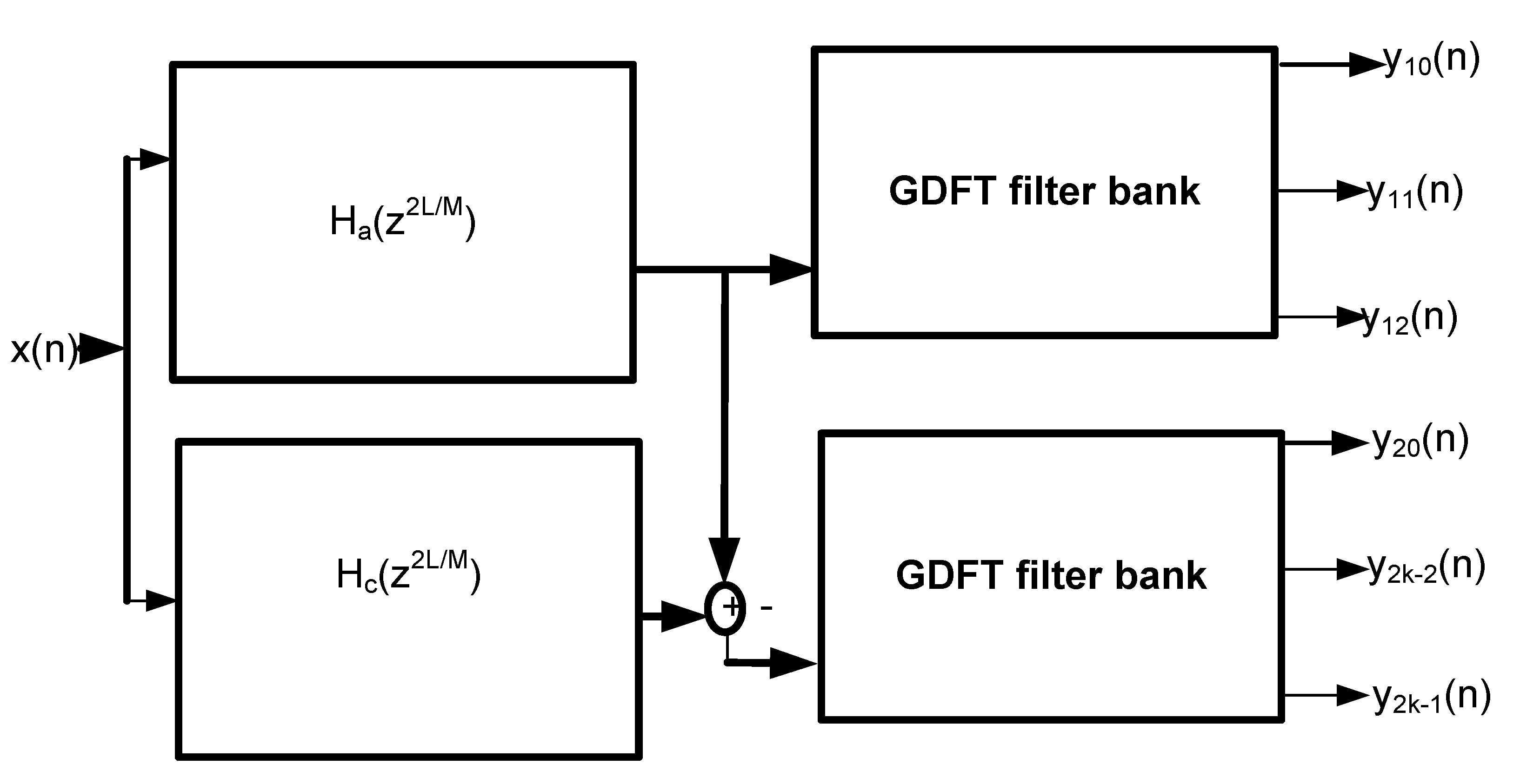
The HGDFT-based filter bank consists of two branches: The upper and the lower branch. The upper branch is made up of FRM-interpolated coefficient decimated filters and the masking filter, whereas the lower branch consists of complementary FRM-interpolated coefficient decimated filters and the complementary masking filter. A low-pass interpolated coefficient decimated linear phase FIR filter, , is formed from the cascade of the base interpolating filter, , and the coefficient decimating filter, , in order to extract the sharp narrow-band channel of choice. Furthermore, a bandpass edge-complementary interpolating coefficient decimated base filter, , is formed from the cascade of the complementary base interpolating filter, , and the complementary coefficient decimating filter, , in order to isolate multi-band frequency responses. The low-pass interpolated coefficient base filter, , cascades with the masking filter, , in the upper branch, while the bandpass complementary interpolated coefficient base filter, , cascades with the complementary masking filter, , in the lower branch, in order to produce reconfigurable low computational multi-narrow frequency bands. The desired passband and cutoff frequency of the base filter response, , are calculated as indicated in Table 2. The transfer function of the FRM interpolated coefficient decimated filter is given by Equation (1), as:
The interpolated coefficient decimated base and complementary filters are symmetrical and asymmetrical linear phase FIR filters, respectively, which can be expressed as . A half band filter is introduced into the FRM Interpolated coefficient decimated filter, in order to further reduce its computational complexity. This is possible as a result of the symmetrical properties possessed by the half-band filter. The time-domain impulse response of the CDM-1 technique requires every other component to be zero, except for the components at the centre. This indicates that it is symmetrical around the centre. This translates to reduced complexity, in terms of the number of the multipliers required by the filter. The transfer function of the half-band FRM interpolated coefficient decimated filter can be expressed in terms of two polyphase components, as in Equation (2):
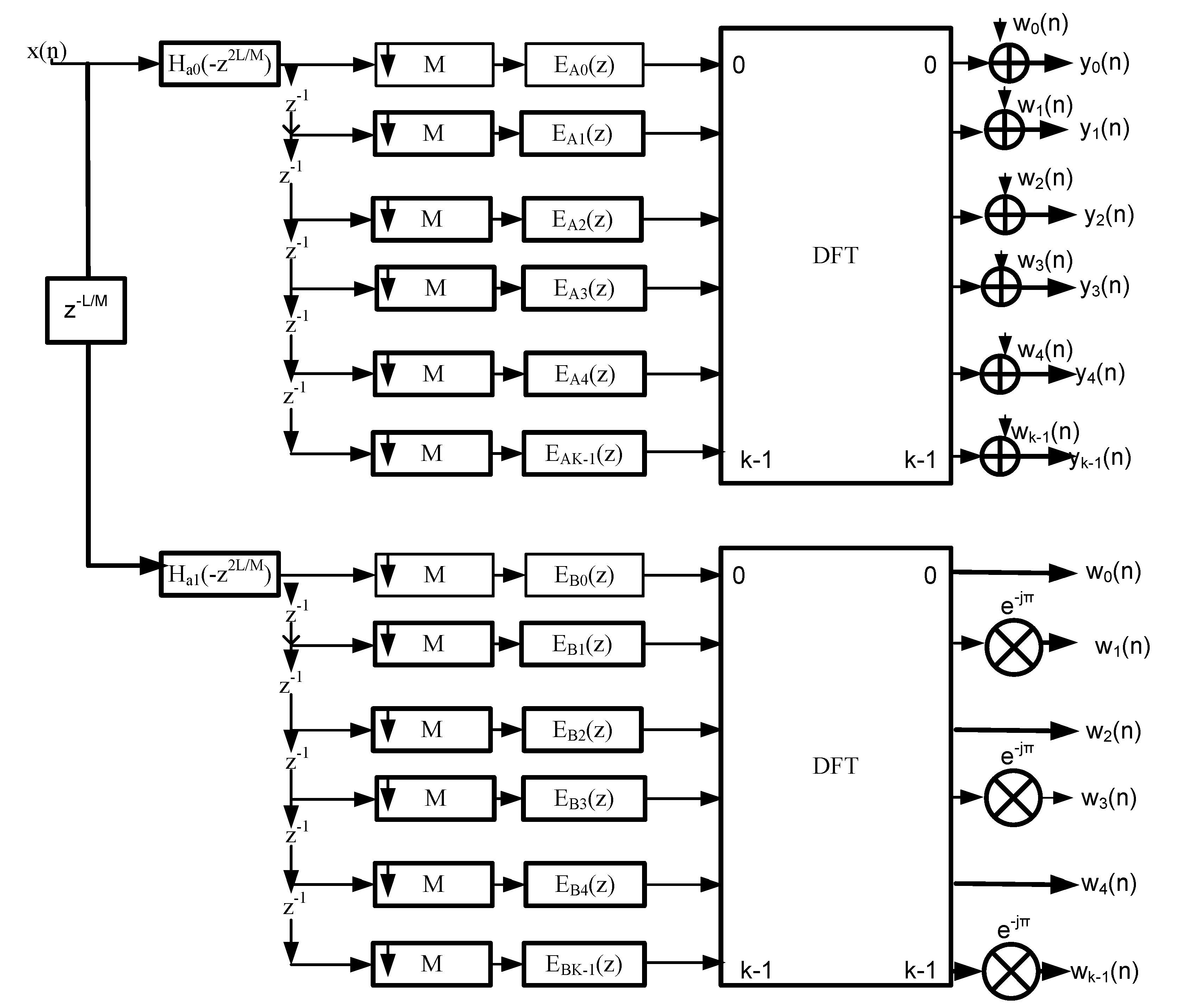
The masking filters are replaced with two GDFT-FBs, as shown in Figure 1. The transfer function for H-GDFT can be expressed as:
By applying polyphase decomposition, Equation (4) is obtained:
where and are the k polyphase components of and , respectively. The GDFT-FB modulated bandpass filters are obtained from the lowpass prototype filter by applying complex modulations, as in Equation (5):
Finally, Equation (6) represents each of the modulated bandpass filters, as depicted in Figure 2:
where =.
The transition band of the H-GDFT FB is centered at rad, whereas the complementary filter bank is centred at , where K is an integer ranging from 0 to .
2.1.1. Proposed Design Steps
The design steps for the proposed filter bank are outlined below:
- Normalise all the channel bandwidths (BWs), such that the and transition bandwidth specifications range from 0 to 1; 1 corresponds to , where is the sampling frequency.
- Calculate each channel stopband frequency, such that .
- Calculate the modal bandwidth such that = GCD/2. This corresponds to the modal stopband frequency.
- Calculate the decimation factor M of the masking filter using the formula M=. The interpolated factor is calculated using the formula , where is the stopband frequency for each channel. Thus, the fractional rate for the masking filter can be calculated as .
- Calculate the decimator factor of the complementary filter using the formula . The interpolated factor is calculated using the formula . Thus, the fractional rate for complementary filter can be calculated as .
- Determine the transition bandwidth for the masking and complementary filters, , such that = , where is the fractional rate for masking or complementary filter.
- Determine the base modal or complementary modal TBW as= min. This corresponds to the modal transition width.
- Calculate the modal, masking, and complementary passband widths using = .
- Determine the passband edge and stopband edge of the modal or prototype filter, masking, and complementary filter, using Table 2, where m = for the masking filter and m = for the complementary filter.
- Find the stopband ripple using = .
- The modal passband peak ripple is calculated as: = min().
- The cutoff frequency of the prototype and masking filter are calculated using Table 2.
- Determine the prototype filter order and the individual channel filter order using the Bellanger formula N = [58].
2.2. Improving HGDFT with Parallel Distributed Arithmetic-Based Residual Number System (PDA-RNS)
In an attempt to lower the filter complexity and improve the reconfigurability of the proposed hybrid filter bank, we propose the design of our second approach, known as the parallel distributive arithmetic-based residual number system. The design and tco-simulation were carried out on the Quartus 11 Altera DSP builder 10, using the very high-speed integrated circuits (VHSIC) hardware description language. Consider an input signal sampling rate of 40 MHz for the filter design example in Section 2.2.1, with the filter specifications given in Table 3. The moduli set , , was selected from the literature, due to its high speed and reduced hardware complexity. With the value of bits, the relevant moduli set based on the moduli format is . The filter coefficients of the reconfigurable filter generated in Table 3 are converted into floating point integer or decimal values. The integer residual values are then transformed from floating point into fixed point values in these two steps. These involve quantizing and discretizing the floating point values using the MATLAB functions, known as quantizer and = . The values of the parameter format create a parameter of binary numbers (word length, fractional length) for signed fixed-point mode. The input signal and the filter coefficients use 16-bit precision format, with a parameter word length of 16 and fractional length = 15.
Distributed arithmetic can be expressed as:
where represents the filter coefficient and denotes the input signal vectors. The fixed-point binary values of the input signals and the filter coefficients are converted into the residue form using the arbitrary forward converter mechanism outlined below. The inputs in Equation (7) are converted to RNS, as shown in Equation (8):
Assume that the input block X is partitioned into different bits, as follows: . Then, the blocks of bits can be represented by
The total residue X is calculated as the total sum of the partitioned residue bits blocks, with respect to the chosen modulus, as depicted in Equation (10):
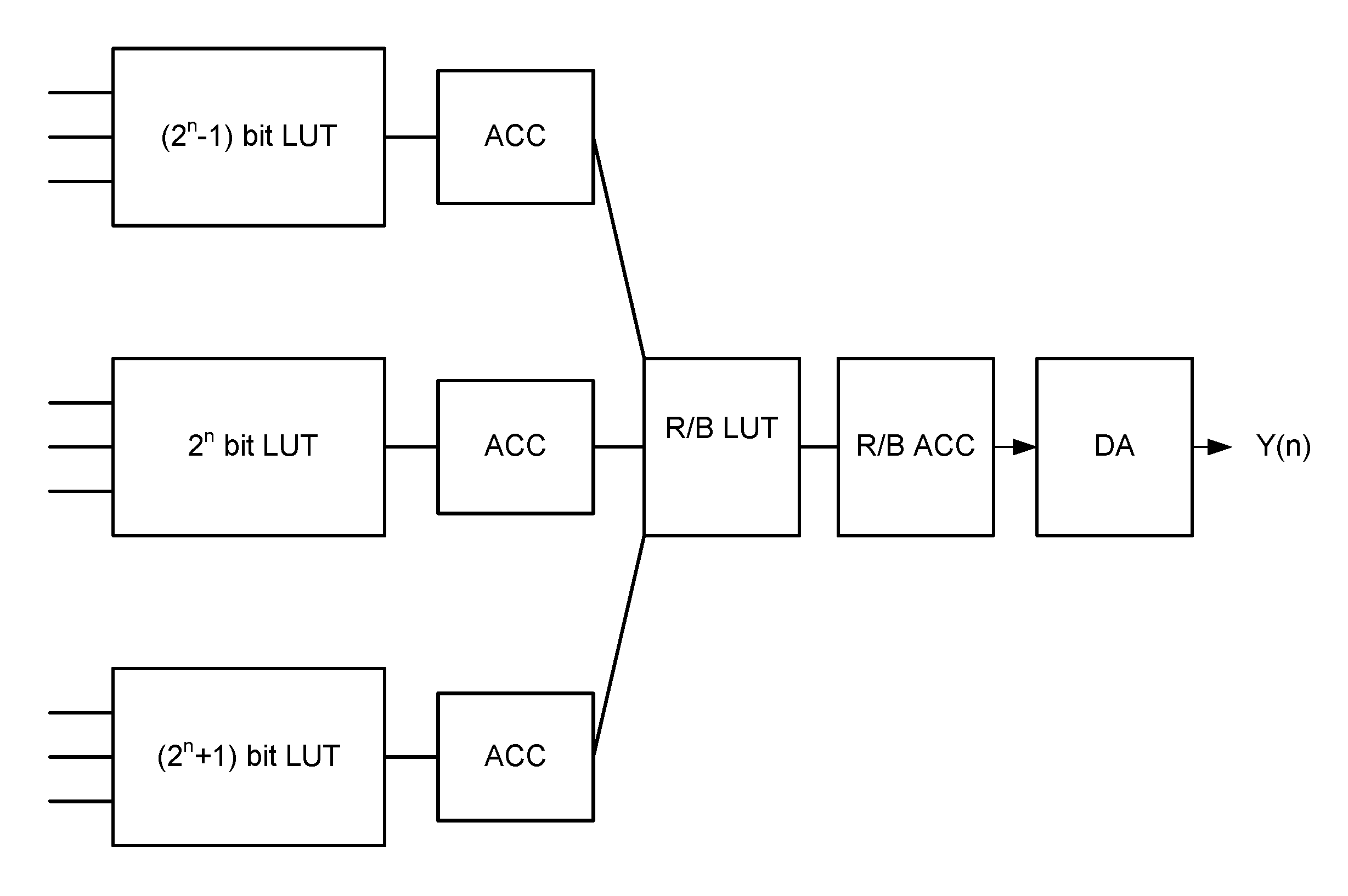
The reverse converter, which converts from residual to binary numbers, takes place at the back-end of the architecture; the shift and add method is used for its implementation. The possible values of , , and are pre-computed and stored in a -bit LUT. After the residual values are computed, Equation (8) becomes Equation (11):
Without loss of generality, let us assume that is an N-bit residual of Q1; that is, an format number, such that
The dot product of (12) can be written as:
Rearranging the terms yields
For and , the rearrangement forms the following entries in the ROM, as indicated in Equation (15):
The input values and filter coefficients pre-stored in the LUT tables are partitioned into different LUT tables and a modulo accumulator (ACC) performs the modulo shift–accumulate operation, in order to generate in D cycles, as shown in Figure 3. Performance comparison was evaluated in terms of the resource utilization, power consumption, and delay.
2.2.1. Application of HGDFT with PDA-RNS Filter Bank to Non-Uniform Channels: BT, ZIGBEE, WCDMA
The HGDFT channelization algorithm was applied to non-uniform input channels. The three multi-standard channels considered were: Bluetooth (BT), Zigbee, and wideband code division multiplexers (WCDMA). The input sampling rate used was MHz, with the channel bandwidths for BT, Zigbee, and WCDMA specified as 1 MHz, 4 MHz, and 5 MHz, respectively. The transition bandwidths for BT, Zigbee, and WCDMA were specified as 50 kHz, 200 kHz, and 500 kHz, respectively. The passband and stopband ripples specifications for BT and Zigbee were and dB, while those of WCDMA channels were and dB, respectively. The filters , , and were the base filter, masking, and complementary filters, respectively, characterised using Case 1 of Table 2. The filter specifications shown in Table 4 were simulated following the design steps in Section 2.1.1. The following parameters were used to compare the performance of the new results: passband and stopband width, passband ripples, and stopband attenuation. The results obtained were compared with the designs in [53,54], using the same filter specifications and parameters. The realized HGDFT filter design specifications are shown in Table 3, Table 4, Table 5, Table 6. The filter coefficients obtained for BT, Zigbee, and WCDMA in Table 3 were revised by converting into RNS format. The double precision bit values for the different filter coefficients were quantized and converted into integer values. These values were transformed into three modular RNS representations. The parallel distributed arithmetic architecture was used for implementing the addition of these three RNS values. The co-simulations of HGDFT with PDA-RNS used the following parameters on the Quartus 11 Altera software: LUT slices, total slices, slice registers and slice LUTs, flip flops, power, and delay. Performance comparisons were made using NU-MDFT CSD optimized with Pareto ABC [55], NU-MDFT SID-CSE [55], Sdr in channeliser [56], and SDR in Channeliser [57].
3. Results and Discussion
Using the information contained in Table 3, the normalized channel bandwidths of Bluetooth (BT), ZigBee, and wide code division multiplexer access (WCDMA) were , , and , respectively. From Step 2 of Section 2.1.1, the passband width of the prototype filter was thus set to .
The fractional rate of each channel was calculated using the formula in Step 3 of Section 2.1.1. The fractional sampling rate for the modal filter was , while the masking filters for BT, Zigbee, and WCDMA were , , and , respectively.
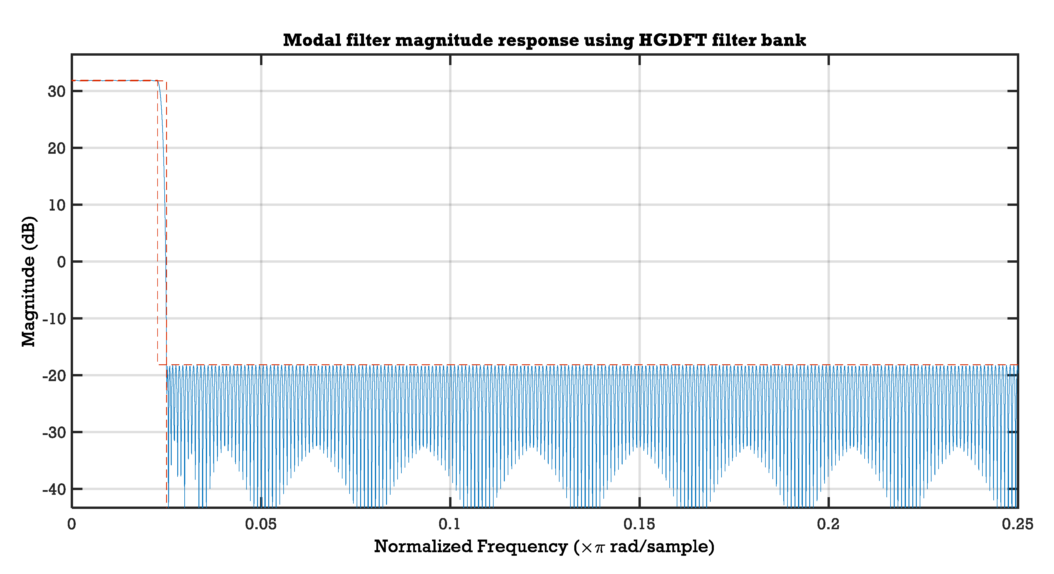
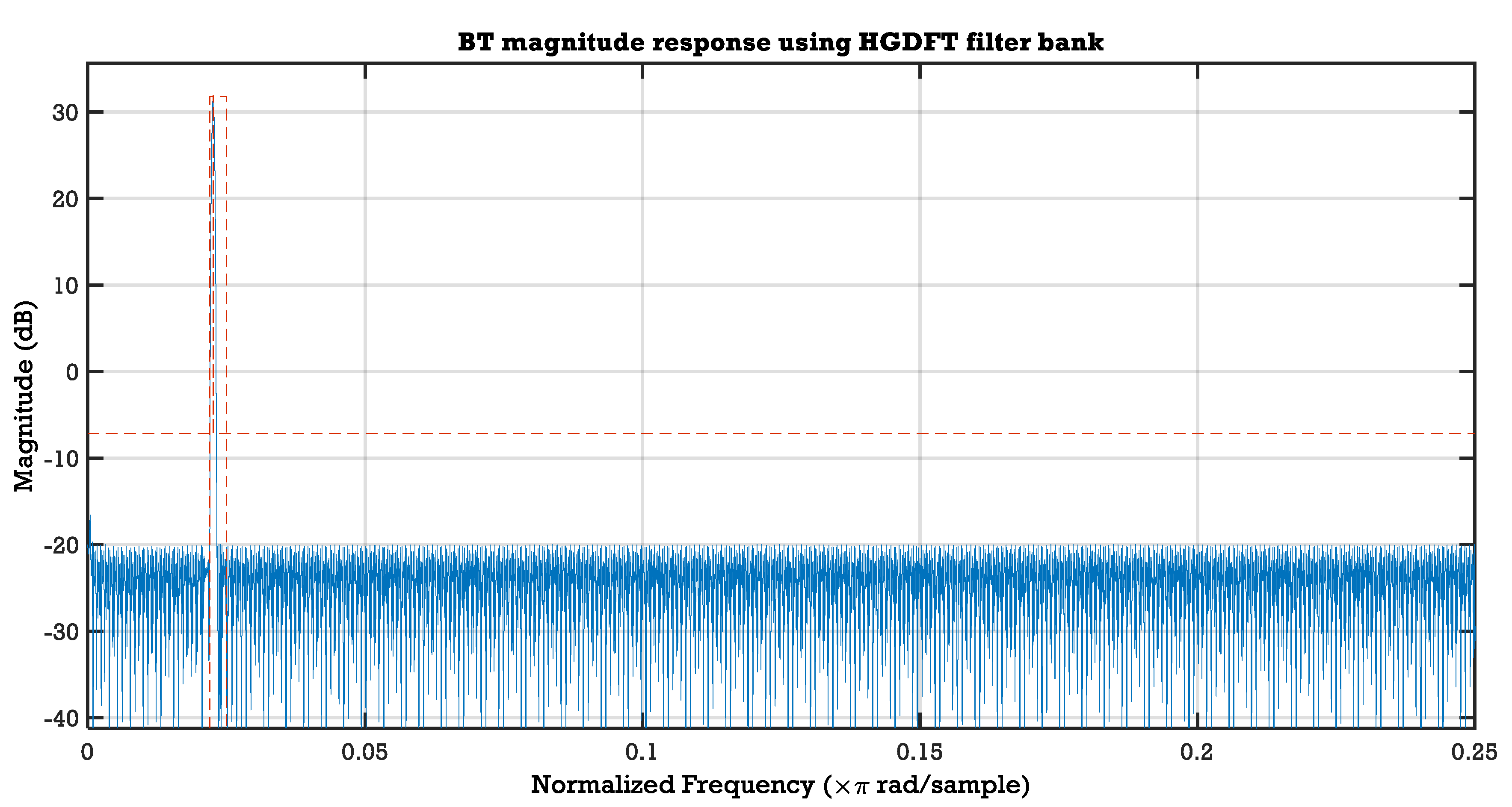
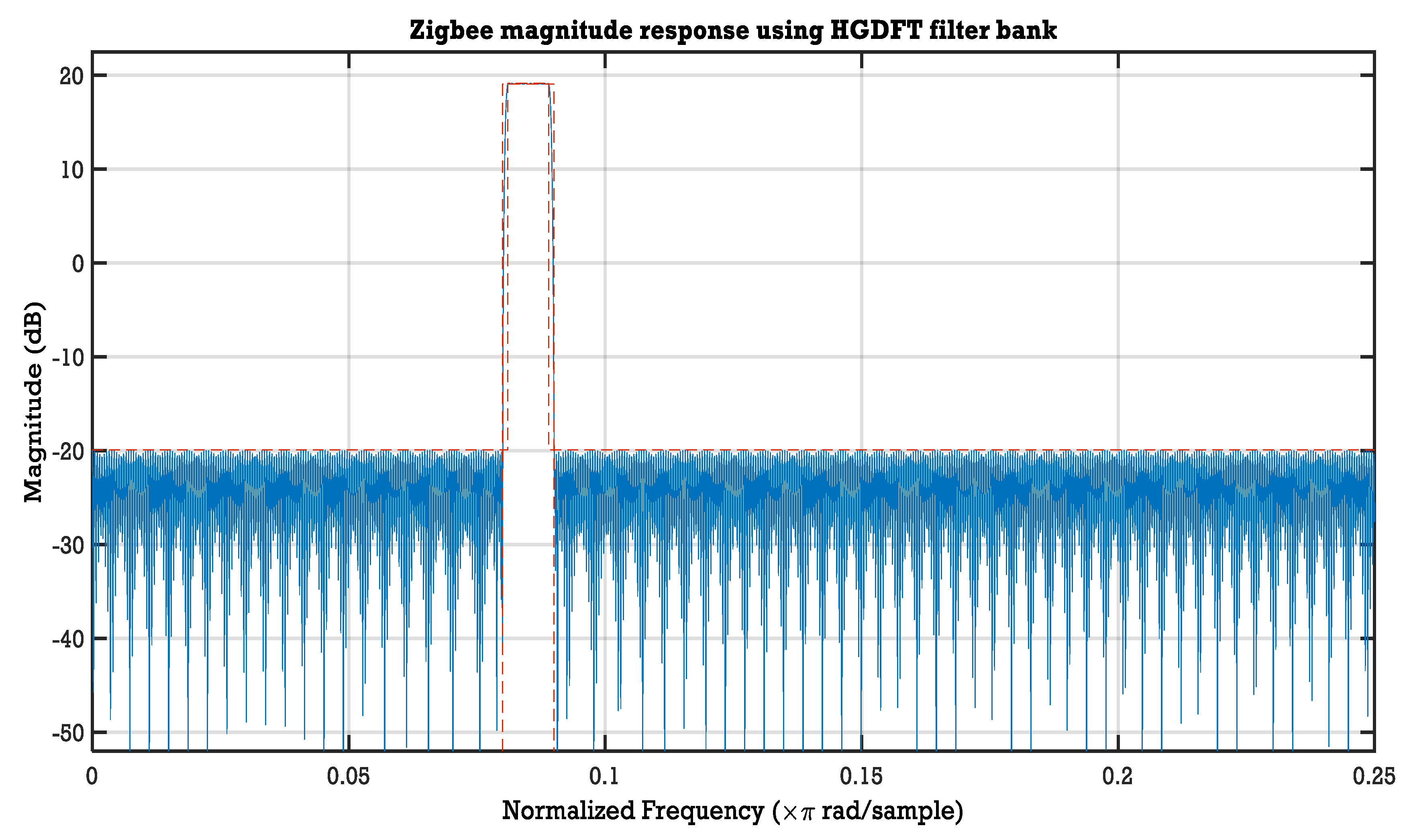
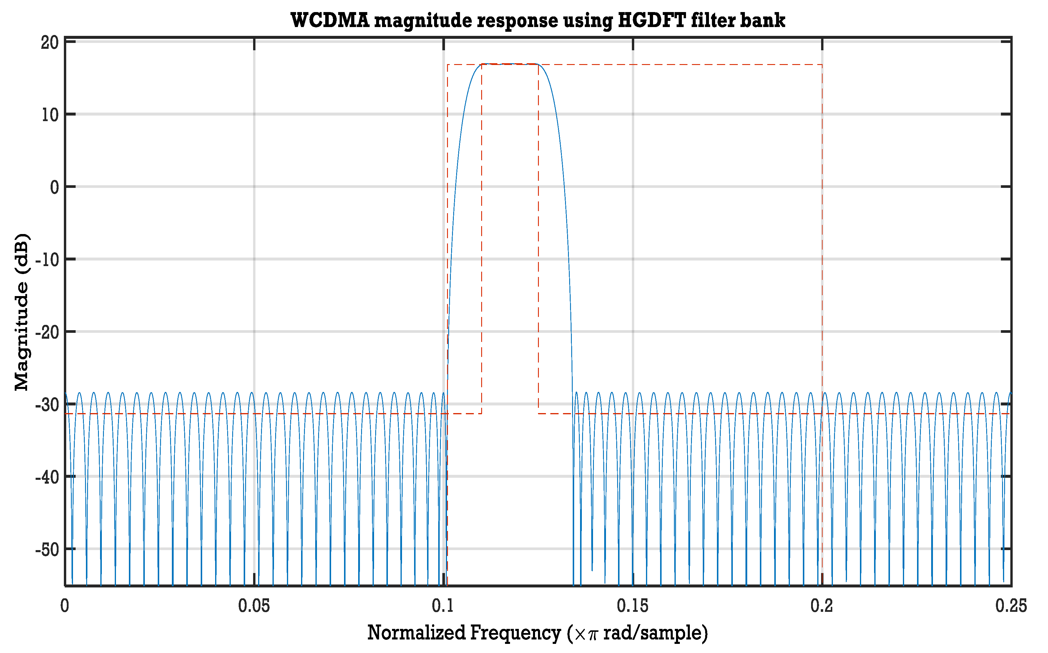
When the fractional rate of was applied to the modal filter, the transition bandwidth computed was , with passband peak ripple of dB, stopband peak ripple of dB, and filter length of 196. When the fractional rate of was applied to the BT channels, the transition bandwidth was , with passband peak ripple of dB, stopband peak ripple of dB, and filter length of 159. When the fractional rate of Zigbee was , the transition bandwidth was calculated to be , with passband ripple of , stopband peak ripple of , and filter order of 34. When the fractional rate of WCDMA was , the transition bandwidth was calculated to be , with passband ripple of , stopband peak ripple of , and filter order of 19. The frequency characteristic input is shown in Table 3, while Figure 4, Figure 5, Figure 6 and Figure 7 show the magnitude responses of the input for the modal filter, BT masking filter, Zigbee masking filter, and WCDMA masking filter.
The stopband for the complementary masking frequency was also calculated, using the equation in Table 2. The stopband edge, passband edge, and fractional rate values were calculated using design steps 5 and 9 in Section 2.1.1. The complementary masking decimator factors for the modal filter, BT, Zigbee, and WCDMA were , , , and , respectively. The complementary masking transition bandwidths for the modal filter, BT, Zigbee, and WCDMA were 0.00222, 0.00222, 0.0089, and 0.021875, with filter order of 209, 150, 37, and 13, respectively. Table 5 shows the filter characteristics of the complementary masking filter using the HGDFT channelisation algorithm.
The total number of multiplications used was 526, while the multiplications used in [53,54,55] were found to be 1745, 1545, and 1090, respectively. The number of multipliers utilized by the proposed HGDFT filter bank was compared and found to be lower than those of the CDFB [54] and ICDM [53,55] methods, as indicated in Table 7.
Figure 5, Figure 6 and Figure 7 show the magnitude responses of the modal filter, BT masking filter, Zigbee masking filter, and WCDMA masking filter.
The results obtained from improving HGDFT with the PDA-RNS filter are as follows. The filter coefficients obtained in Table 2 were quantized with 16-bit representation, as it showed better passband ripples and stopband attenuation, when compared with 8- and 12-bit representations, as indicated in Table 8. By replacing the multiplier in the HGDFT with the PDA-RNS filter, there was an 100% decrease in multipliers, from 526 to 0, as the use of multipliers was totally eliminated.
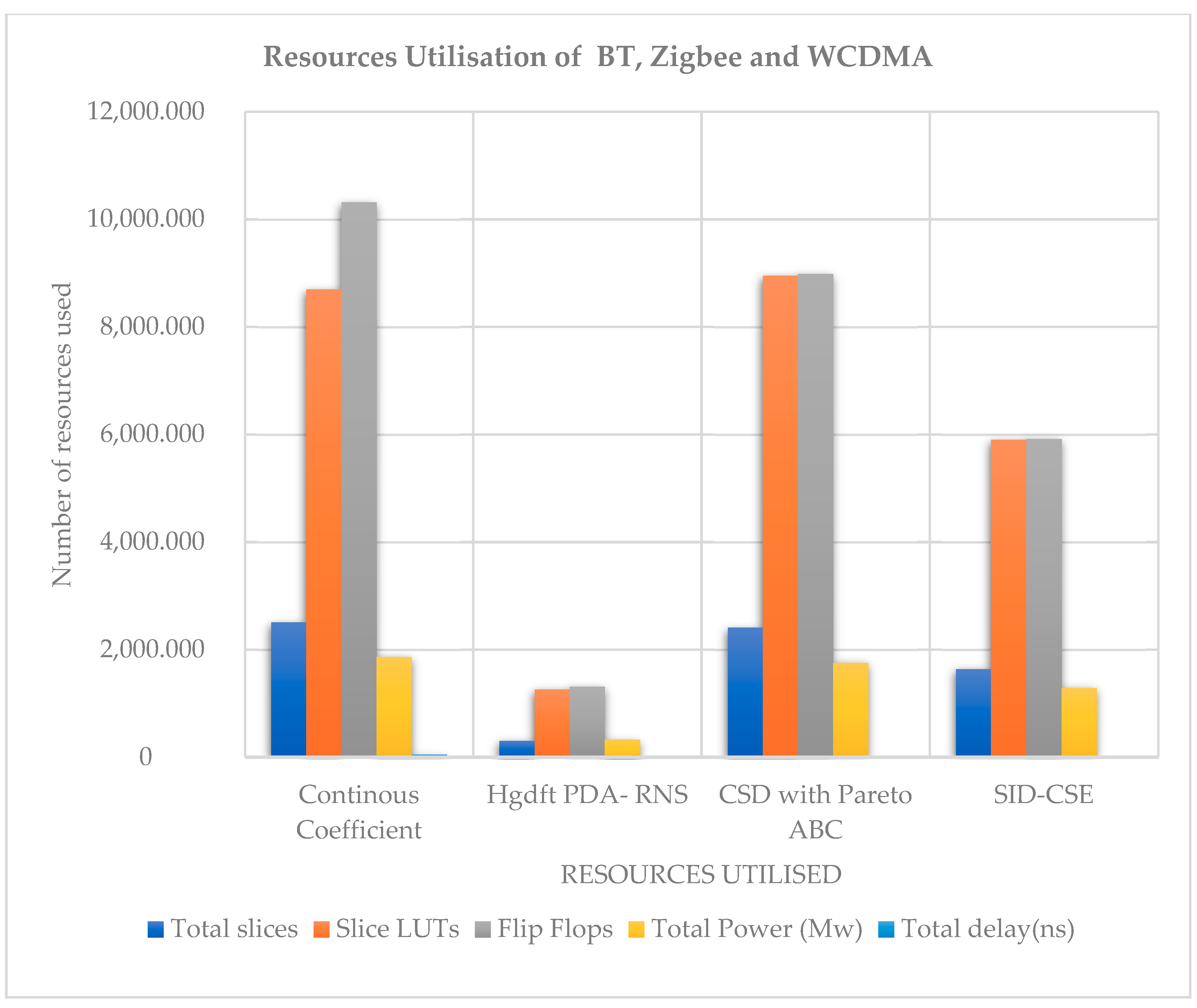
Table 9, Table 10 show a device utilization comparison. The total hardware resources occupied by HGDFT with PDA-RNS were as follows: 941 total slices, 2073 slices of LUTs, 2338 flip-flops, total power of 333.53 mW, and total delay of 3.328 ns. The total slices occupied by NU-MDFT CSD with Pareto ABC were 2406, slice LUTs utilized were 8950, flip flops consumed were 8980, total power consumed was 1751 mW, and total delay of 3.75 ns. The performance of the NU-MDFT filter optimized with SID-CSE showed total slices consumed of 1633, slice LUTs utilized of 5901 with flip flops of 5911, total power of 1281 mW, and delay time 2.6 ns.
From these performance results, the plot in Figure 8 shows that HGDFT with PDA-RNS utilized % of the total LUT, 14% of the LUT slices, had a % reduction in flip-flops used, 17% power consumption, and 4% delay in the execution time, when compared with NU-MDFT CSD optimized with Pareto ABC [55]. It was observed that the filter achieved an 83% reduction in number of occupied slices, from 2406 to 941 slices. There was an 83% reduction in power consumption and 75% reduction in execution delay time. However, when HGDFT PDA-RNS filter was compared with the NU-MDFT SID-CSE in [55], the delay execution time for NU-MDFT SIDE-CSE was found to be lower and, thus, faster.
The total resources utilised are compared in Table 10. The slice registers utilized by HGDFT with PDA-RNS filter bank were 2279 out of 239,616. This showed a drastic reduction in slice registers, when compared with NU MDFT FB in [55], which consumed 29,797 out of 301,440; that in [56], which used 15,295 out of 58,880; and also that in [57], which used up 29,797 out of 301,440. The total slice LUTs used by HGDFT with PDA-RNS filter were found to be 2022 out of 119,808, while the hardware utilized by the NU MDFT filter in [55] was observed to use 5901 out of 298,600, the device consumption rate in [57] was discovered to be 21,169 out of 150,720, and that in [56] used up 14,726 out of 58,880. Thus, Table 10 proves that the hardware resource utilization under the implementation of HGDFT with the PDA-RNS filter bank was less than that in SDR channeliser [55,56,57]. The lower filter order of the proposed design, coupled with the modularity of RNS, clearly contributed to its lower slice requirements and lower power consumption, when compared to the designs in [39,55].
4. Conclusions
The proposed HGDFT with PDA-RNS method was found to be an effective channelization algorithm for low-complexity reconfigurable filters in multi-standard receivers. Two improvement methods were used for the realization of the algorithm: The first improvement was achieved by hybridizing CD1 and FRM filters with the GDFT. The performance of the method was further improved by using a parallel distributed arithmetic-based residue number system. The HGDFT filter bank demonstrated a reduction in the number of multiplications and filter coefficients used, compared with FRM-based or modified GDFT. The HGDFT filter bank was also optimized with a PDA-RNS, after which it was shown that the number of adders, multipliers, and overall filter complexity were reduced to the barest minimum, while reconfigurability was preserved. This resulted in remarkable reductions in resource utilization, operational speed, and power consumption.
Author Contributions
Conceptualization, T.O.O.; methodology, T.O.O.; software, T.O.O.; validation, T.O.O.; formal analysis, T.O.O.; investigation, T.O.O.; resources, T.O.O.; data curation, T.O.O.; writing—original draft preparation, T.O.O.; writing—review and editing, T.O.O.; visualization, T.O.O.; supervision, H.C.M.; project administration, T.O.O.; funding acquisition, H.C.M. All authors have read and agreed to the published version of the manuscript.
Funding
This research received no external funding.
Conflicts of Interest
The authors declare no conflict of interest.
References
- Boucheret, M.L.; Mortensen, I.; Favaro, H. Fast convolution filter banks for satellite payloads with on-board processing. IEEE J. Sel. Areas Commun. 1999, 17, 238–248. [Google Scholar] [CrossRef]
- Lillington, J. Comparison of wideband channelisation architectures. In Proceedings of the International Signal Processing Conference (ISPC), Dallas, TX, USA, 31 March–3 April 2003. [Google Scholar]
- Deshmukh, T.P.; Deshmukh, P.; Dakhole, P. Design of cyclotomic Fast Fourier Transform architecture over Galois field for 15 point DFT. In Proceedings of the 2015 International Conference on Industrial Instrumentation and Control (ICIC), Pune, India, 28–30 May 2015; pp. 607–611. [Google Scholar]
- Diniz, P.S.; Da Silva, E.A.; Netto, S.L. Digital Signal Processing: System Analysis and Design; Cambridge University Press: Cambridge, UK, 2010; pp. 259–299. [Google Scholar]
- Navarro, A.P. Overlapped polyphase DFT modulated filter banks applied to TETRA/TEDS SDR base station channelization. In Proceedings of the Royal Irish Academy Communication and Radio Science Colloquium, Dublin, Ireland, 21–22 April 2010. [Google Scholar]
- Tietche, B.H.; Romain, O.; Denby, B. Sparse channelizer for FPGA-based simultaneous multichannel DRM30 receiver. IEEE Trans. Consum. Electron. 2015, 61, 151–159. [Google Scholar] [CrossRef]
- Duhamel, P.; Vetterli, M. Fast Fourier transforms: A tutorial review and a state of the art. Signal Process. 1990, 19, 259–299. [Google Scholar] [CrossRef] [Green Version]
- Crochiere, R.E.; Rabiner, L.R. Multirate Digital Signal Processing, 1983; Pretice Hall: Upper Saddle River, NJ, USA, 1987; pp. 127–192. [Google Scholar]
- Cooley, J.W.; Tukey, J.W. An algorithm for the machine calculation of complex Fourier series. Math. Comput. 1965, 19, 297–301. [Google Scholar] [CrossRef]
- Abu-Al-Saud, W.A.; Stuber, G.L. Efficient wideband channelizer for software radio systems using modulated PR filterbanks. IEEE Trans. Signal Process. 2004, 52, 2807–2820. [Google Scholar] [CrossRef]
- Kalathil, S.; Elias, E. Non-uniform cosine modulated filter banks using meta-heuristic algorithms in CSD space. J. Adv. Res. 2015, 6, 839–849. [Google Scholar] [CrossRef] [Green Version]
- Blok, M. Fractional delay filter design for sample rate conversion. In Proceedings of the 2012 Federated Conference on Computer Science and Information Systems (FedCSIS), Wroclaw, Poland, 9–12 September 2012; pp. 701–706. [Google Scholar]
- Valimaki, V.; Haghparast, A. Fractional delay filter design based on truncated Lagrange interpolation. IEEE Signal Process. Lett. 2007, 14, 816–819. [Google Scholar] [CrossRef]
- Karp, T.; Fliege, N.J. MDFT filter banks with perfect reconstruction. In Proceedings of the ISCAS’95-International Symposium on Circuits and Systems, Seattle, WA, USA, 30 April–3 May 1995; Volume 1, pp. 744–747. [Google Scholar]
- Farrow, C.W. A continuously variable digital delay element. In Proceedings of the 1988 IEEE International Symposium on Circuits and Systems, Espoo, Finland, 7–9 June 1988; pp. 2641–2645. [Google Scholar]
- Kuldeep, B.; Kumar, A.; Singh, G. Design of quadrature mirror filter bank using Lagrange multiplier method based on fractional derivative constraints. Eng. Sci. Technol. Int. J. 2015, 18, 235–243. [Google Scholar] [CrossRef] [Green Version]
- Vaidyanathan, P.P. Multirate Systems and Filter Banks; Pearson Education: Tamil Nadu, India, 1993. [Google Scholar]
- Brannon, B.; Efstathiou, D.; Gratzek, T. A look at software radios: Are they fact or fiction? Electron. Des. 1998, 46, 117–122. [Google Scholar]
- Chang, Z.; Vinod, A.; Meher, P. Reconfigurable architectures for low complexity software radio channelizers using hybrid filter banks. In Proceedings of the 2006 10th IEEE Singapore International Conference on Communication Systems, Singapore, 30 October–1 November 2006; pp. 1–5. [Google Scholar]
- Harris, F.; McGwier, R. A receiver structure that performs simultaneous spectral analysis and time series channelization. In Proceedings of the SDR’09 Technical Conference and Product Exposition, Washington, DC, USA, 1–4 December 2009. [Google Scholar]
- Navarro, Á.P. Channelization for Multi-Standard Software-Defined Radio Base Stations. Ph.D. Thesis, National University of Ireland Maynooth, Maynooth, Ireland, 2011. [Google Scholar]
- Palomo-Navarro, Á.; Farrell, R.J.; Villing, R. Combined FRM and GDFT filter bank designs for improved nonuniform DSA channelisation. Wirel. Commun. Mob. Comput. 2016, 16, 1440–1456. [Google Scholar] [CrossRef]
- Sudharman, S.; Rajan, A.D.; Bindiya, T. Design of a Power-Efficient Low-Complexity Reconfigurable Non-maximally Decimated Filter Bank for High-Resolution Wideband Channels. Circuits Syst. Signal Process. 2019, 38, 2703–2735. [Google Scholar] [CrossRef]
- Ambede, A.; Smitha, K.; Vinod, A.P. Flexible low complexity uniform and nonuniform digital filter banks with high frequency resolution for multistandard radios. IEEE Trans. Very Large Scale Integr. Syst. 2014, 23, 631–641. [Google Scholar] [CrossRef]
- Lovina, P.; Manjusha, K.A. SDR Applications using VLSI Design of Reconfigurable Devices. IJSRST 2018, 4, 1148–1153. [Google Scholar]
- Peng, X.; Li, J.; Zhou, X.; Lin, Q.; Chen, Z. Analysis and design of M-channel hybrid filter bank with digital calibration. IEEE Access 2018, 6, 24606–24616. [Google Scholar] [CrossRef]
- Badave, S.; Bhalchandra, A. Critical Path Reduction of Distributed Arithmetic Based FIR Filter. Int. J. Adv. Comput. Sci. Appl. 2016, 7, 71–78. [Google Scholar] [CrossRef] [Green Version]
- Singh, S.; Saini, S. Performance Analysis of FIR Filter Using Distributed Arithmetic. Glob. J. Comput. Technol. 2017, 5, 310–313. [Google Scholar]
- Naik, N.S.; Gupta, K.A. An efficient reconfigurable FIR digital filter using modified distribute arithmetic technique. arXiv 2017, arXiv:1704.08526. [Google Scholar]
- Yoo, H.; Anderson, D.V. Hardware-efficient distributed arithmetic architecture for high-order digital filters. In Proceedings of the (ICASSP’05) IEEE International Conference on Acoustics, Speech, and Signal Processing, Philadelphia, PA, USA, 23–23 March 2005; Volume 5, pp. 5–125. [Google Scholar]
- White, S.A. Applications of distributed arithmetic to digital signal processing: A tutorial review. IEEE Assp Mag. 1989, 6, 4–19. [Google Scholar] [CrossRef]
- Chen, C.C.; Lin, T.J.; Liu, C.W.; Jen, C.W. Complexity-aware design of a DA-based FIR filters. In Proceedings of the 2004 IEEE Asia-Pacific Conference on Circuits and Systems, Tainan, Taiwan, 6–9 December 2004; Volume 1, pp. 445–448. [Google Scholar]
- Longa, P.; Miri, A. Area-efficient FIR filter design on FPGAs using distributed arithmetic. In Proceedings of the 2006 IEEE International Symposium on Signal Processing and Information Technology, Vancouver, BC, Canada, 27–30 August 2006; pp. 248–252. [Google Scholar]
- Iruleswari, M.; Sheela Merlin, M.; Jeyapaul Murugan, A. Design and Implementation of distributed arithmetic technique based FIR filter using lookup table. Int. J. Innov. Res. Sci. Eng. Technol. 2016, 5, 3480–3488. [Google Scholar]
- Roy, K.J.; Ramya, R. Low-Power And Low-Area Adaptive FIR Filter Based on Distributed Arithmetic and LMS Algorithm. IJSRP 2014, 4, 1–5. [Google Scholar]
- Kalaiyarasi, D.; Reddy, T.K. Design and implementation of least mean square adaptive FIR filter using offset binary coding based distributed arithmetic. Microprocess. Microsyst. 2019, 71, 102884. [Google Scholar] [CrossRef]
- Bindiya, T.S.; Kumar, V.S.; Elias, E. Design of low power and low complexity multiplier-less reconfigurable non-uniform channel filter using genetic algorithm. Glob. J. Res. Eng. 2012, 12, 7–19. [Google Scholar]
- Bindiya, T.; Elias, E. Modified metaheuristic algorithms for the optimal design of multiplier-less non-uniform channel filters. Circuits Syst. Signal Process. 2014, 33, 815–837. [Google Scholar] [CrossRef]
- Srinivasa Reddy, K.; Sahoo, S.K. An approach for fixed coefficient RNS-based FIR filter. Int. J. Electron. 2017, 104, 1358–1376. [Google Scholar] [CrossRef]
- Andraos, S.; Ahmad, H. A new efficient memoryless residue to binary converter. IEEE Trans. Circuits Syst. 1988, 35, 1441–1444. [Google Scholar] [CrossRef]
- Molahosseini, A.S.; Navi, K. New arithmetic residue to binary converters. IJCSES 2007, 1, 296. [Google Scholar]
- Premkumar, A.B. An RNS to binary converter in a three moduli set with common factors. IEEE Trans. Circuits Syst. II Analog. Digit. Signal Process. 1995, 42, 298–301. [Google Scholar] [CrossRef]
- Premkumar, A.B.; Bhardwaj, M.; Srikanthan, T. High-speed and low-cost reverse converters for the (2n − 1, 2n, 2n + 1) moduli set. IEEE Trans. Circuits Syst. II Analog. Digit. Signal Process. 1998, 45, 903–908. [Google Scholar] [CrossRef]
- Vun, C.H.; Premkumar, A.B.; Zhang, W. A new RNS based DA approach for inner product computation. IEEE Trans. Circuits Syst. I Regul. Pap. 2013, 60, 2139–2152. [Google Scholar] [CrossRef]
- Živaljević, D.; Stamenković, N.; Stojanović, V. Digital filter implementation based on the RNS with diminished-1 encoded channel. In Proceedings of the 2012 35th International Conference on Telecommunications and Signal Processing (TSP), Prague, Czech Republic, 3–4 July 2012; pp. 662–666. [Google Scholar]
- Vergos, H.T.; Efstathiou, C. A unifying approach for weighted and diminished-1 modulo 2 n+1 addition. IEEE Trans. Circuits Syst. II Express Briefs 2008, 55, 1041–1045. [Google Scholar] [CrossRef]
- Singh, R.; Mishra, R. Design and Simulation of Diminished-One Modulo 2n+ 1 Adder Using Circular Carry Selection. In Proceedings of the World Congress on Engineering, London, UK, 6–8 July 2011. [Google Scholar]
- Mohan, P.A. Evaluation of fast conversion techniques for binary-residue number systems. IEEE Trans. Circuits Syst. Fundam. Theory Appl. 1998, 45, 1107–1109. [Google Scholar] [CrossRef]
- Skavantzos, A.; Abdallah, M. Implementation issues of the two-level residue number system with pairs of conjugate moduli. IEEE Trans. Signal Process. 1999, 47, 826–838. [Google Scholar] [CrossRef]
- Conway, R.; Nelson, J. Fast converter for 3 moduli RNS using new property of CRT. IEEE Trans. Comput. 1999, 852–860. [Google Scholar] [CrossRef]
- Gbolagade, K.A.; Voicu, G.R.; Cotofana, S.D. An Efficient FPGA Design of Residue-to-Binary Converter for the Moduli Set. IEEE Trans. Very Large Scale Integr. Syst. 2011, 19, 1500–1503. [Google Scholar] [CrossRef]
- Hiasat, A. A Residue-to-Binary Converter for the Extended Four-Moduli Set. IEEE Trans. Very Large Scale Integr. Syst. 2017, 25, 2188–2192. [Google Scholar] [CrossRef]
- Ambede, A.; Shreejith, S.; Vinod, A.P.; Fahmy, S.A. Design and realization of variable digital filters for software-defined radio channelizers using an improved coefficient decimation method. IEEE Trans. Circuits Syst. II Express Briefs 2016, 63, 59–63. [Google Scholar] [CrossRef]
- Mahesh, R.; Vinod, A.P.; Lai, E.M.; Omondi, A. Filter bank channelizers for multi-standard software defined radio receivers. J. Signal Process. Syst. 2011, 62, 157–171. [Google Scholar] [CrossRef]
- Sakthivel, V.; Elias, E. Low complexity reconfigurable channelizers using non-uniform filter banks. Comput. Electr. Eng. 2018, 68, 389–403. [Google Scholar]
- Devi, P.K.; Bhuvaneshwaran, R. FPGA implementation of coefficient decimated polyphase filter bank structure for multistandard communication receiver. J. Theor. Appl. Inf. Technol. 2014, 64, 298–306. [Google Scholar]
- Cappello, S.; Cardarilli, G.; Di Nunzio, L.; Fazzolari, R.; Re, M.; Albicocco, P. Flexible channel extractor for wideband systems based on polyphase filter bank. J. Theor. Appl. Inf. Technol. 2017, 95, 3841–3850. [Google Scholar]
- Bellanger, M. On computational complexity in digital filters. In Proceedings of the European Conference on Circuit Theory and Design, Hague, The Netherlands, 25–28 August 1981; pp. 58–63. [Google Scholar]
Figure 1.
Block Diagram of FRM-Interpolated Coefficient Decimated FIR Filter.

Figure 2.
Diagram depicting hybrid generalized discrete Fourier transform (HGDFT) Channelisation Algorithm.
Figure 2.
Diagram depicting hybrid generalized discrete Fourier transform (HGDFT) Channelisation Algorithm.

Figure 3.
Distributed Arithmetic of the three moduli residual number system (RNS) filters.

Figure 4.
Magnitude response for the modal filter.

Figure 5.
Magnitude response for the Bluetooth masking filter.

Figure 6.
Magnitude response for the Zigbee masking filter.

Figure 7.
Magnitude response for the WCDMA masking filter.

Figure 8.
Plot of resource utilization under different filter designs.


Table 1.
Comparison of the different channelization algorithms.
| Channelisation Technique | Computational Load | Reconfigurability |
|---|---|---|
| Per Channel [1,2,3] | Very High | Bad |
| Binary Approach [4] | High | Bad |
| DFT [5] | Very High | Bad |
| DFT (poly-phase) [6,7,8,9] | High | Bad |
| EMFB [10,11] | Low | Bad |
| FPCC [12,13,14,15] | Low | Bad |
| QMFB [16,17] | High | Bad |
| TQMB [18] | High | Good |
| GDFT [5] | High | Good |
| HTQMB [19,20] | High | Good |
| PGDFT [10,21] | High | Good |
| RGDFT [10,22] | High | Good |
| FRM [22,53] | High | Good |
| CDM 1 and 11 [23,24,25,26] | Low | Bad |
| MCD 1 and 11 [23,24,25,26] | Low | Bad |
| ICDM 1 and 11 | Low | Bad |
Very High: higher filter order and filter coefficients; Low: low filter order and filter coefficients; Good: easy to adapt to different standards on the same platform; and Bad: not easy to adapt to different standards on the same device.
Table 2.
Cutoff frequencies of the prototype, masking, and complementary filters.
| Parameter | Case 1 | Case 2 |
|---|---|---|
| = | = | |
| = | = | |
| = | = | |
| = | = |
Table 3.
Frequency characteristics of masking filters implemented using the HGDFT filter bank.
|
Filter Bank |
Stopband Frequency () |
Passband Frequency () |
Stopband Attenuation () |
Passband Ripples () |
Filter Length | |
|---|---|---|---|---|---|---|
| Modal filter, | 0.025 | 0.022625 | 0.1 | −50 | 196 | |
| Bluetooth, | 0.025 | 0.0224 | 0.0975 | −39 | 159 | |
| Zigbee, | 0.1 | 0.089 | 0.09 | −39 | 34 | |
| WCDMA, | 0.2 | 0.125 | 0.0875 | −48.25 | 13 |
Table 4.
Filter specification for the three multi-standard channels.
| Filter Specification | Sampling Frequency (MHz) | Channel Bandwidth (MHz) | Transition Bandwidth (kHz) | Passband Ripples (dB) | Stopband Ripples (dB) |
|---|---|---|---|---|---|
| Bluetooth | 40 | 1 | 50 | 0.1 | −40 |
| Zigbee | 40 | 4 | 200 | 0.1 | −40 |
| WCDMA | 40 | 5 | 500 | 0.1 | −55 |
Table 5.
Frequency characteristics of complementary masking filter implemented using the HGDFT filter bank.
Table 5.
Frequency characteristics of complementary masking filter implemented using the HGDFT filter bank.
| Filter Bank | Passband Frequency () | Stopband Frequency () | Stopband Attenuation () | Passband Ripples () | Filter Length | |
|---|---|---|---|---|---|---|
| Modal filter, | 0.027307 | 0.02269 | 0.1 | −50 | 209 | |
| Bluetooth, | 0.027307 | 0.02269 | 0.092 | −36.92 | 150 | |
| Zigbee, | 0.1080 | 0.0911 | 0.088 | −35.5 | 37 | |
| WCDMA, | 0.2 | 0.125 | 0.0875 | −48.25 | 13 |
Table 6.
Multiplication complexity for non-uniform filter bank.
| Filter Bank | Filter Order | Total Number of Multiplication | ||
|---|---|---|---|---|
| Modal filter | 405 | - | - | 320 |
| BT | - | 159 | 150 | 156 |
| Zigbee | - | 34 | 37 | 37 |
| WCDMA | - | 13 | 13 | 13 |
Table 7.
Multiplication complexity for non-uniform filter bank.
| Filter Bank | Filter Order | Total Number of Multiplication | ||
|---|---|---|---|---|
| CDFB [54] | 3089 | 400 | - | 1745 |
| ICDM FB [53] | 2929 | 160 | - | 1545 |
| NU-MDFT FB [55] | 187 | 430 | 469 | 1090 |
| Proposed HGDFT filter bank Bank | 320 | 104 | 102 | 526 |
Table 8.
Comparison of filter specifications, in terms of number of bits.
| Filter | Input Bits | Passband Filter PB Ripples(dB) | Stopband Attenuation | No of Adders | Amp-Litude Distor-Tion |
|---|---|---|---|---|---|
| Prototype filter | 8-bits | 3.360 | 11.204 | 0.20 | |
| 12-bits | 0.087 | 48.146 | 391 | 0.205 | |
| 16-bits | 0.09 | 48.146 | 0.19 | ||
| Bluetooth | 8-bits | 3.457 | 10.532 | 0.05 | |
| 12-bits | 0.094 | 42.818 | 150 | 0.054 | |
| 16-bits | 0.022 | 43.062 | 0.047 | ||
| Zigbee filter | 8-bits | 0.089 | 39.095 | 0.164 | |
| 12-bits | 0.088 | 39.094 | 34 | 0.164 | |
| 16-bits | 0.089 | 39.094 | 0.164 | ||
| WCDMA | 8-bits | 0.146 | 43.638 | 0.28 | |
| 12-bits | 0.068 | 50.314 | 13 | 0.276 | |
| 16-bits | 0.068 | 50.34 | 0.27 |
Table 9.
Device and power utilization.
| Parameter | NU-MDFT Continous Coefficients | HGDFT with PDA-RNS | NU-MDFT CSD with Pareto ABC [55] | NU-MDFT SID-CSE [55] |
|---|---|---|---|---|
| Total slices | 2507 | 941 | 2406 | 1633 |
| Slice LUTs | 8694 | 2073 | 8950 | 5901 |
| Flip flops | 10,313 | 2338 | 8980 | 5911 |
| Total Power (mW) | 1865 | 333.53 | 1751 | 1281 |
| Total Delay (ns) | 45.125 | 3.328 | 3.75 | 2.6 |
Table 10.
Comparison of device utilization.
| Parameter | SDR in [56] | SDR Channelizer in [57] |
SDR Channelizer Using NU MDFT FB [55] |
Proposed HGDFT with PDA-RNS FB |
|---|---|---|---|---|
| Slice Registers | 15,295 out of 58,880 | 29,797 out of 301,440 | 5880 out of 597,200 | 2279 out of 23,9616 |
| Slice LUTs | 14,726 out of 58,880 | 21,169 out of 150,720 | 5901 out of 298,600 | 2022 out of 119,808 |
Publisher’s Note: MDPI stays neutral with regard to jurisdictional claims in published maps and institutional affiliations. |
© 2020 by the authors. Licensee MDPI, Basel, Switzerland. This article is an open access article distributed under the terms and conditions of the Creative Commons Attribution (CC BY) license (http://creativecommons.org/licenses/by/4.0/).
Share and Cite
MDPI and ACS Style
Otunniyi, T.O.; Myburgh, H.C. Improving Generalized Discrete Fourier Transform (GDFT) Filter Banks with Low-Complexity and Reconfigurable Hybrid Algorithm. Digital 2021, 1, 1-17. https://0-doi-org.brum.beds.ac.uk/10.3390/digital1010001
AMA Style
Otunniyi TO, Myburgh HC. Improving Generalized Discrete Fourier Transform (GDFT) Filter Banks with Low-Complexity and Reconfigurable Hybrid Algorithm. Digital. 2021; 1(1):1-17. https://0-doi-org.brum.beds.ac.uk/10.3390/digital1010001
Chicago/Turabian StyleOtunniyi, Temidayo O., and Hermanus C. Myburgh. 2021. "Improving Generalized Discrete Fourier Transform (GDFT) Filter Banks with Low-Complexity and Reconfigurable Hybrid Algorithm" Digital 1, no. 1: 1-17. https://0-doi-org.brum.beds.ac.uk/10.3390/digital1010001