
Active Balun with Center-Tapped Inductor and Double-Balanced Gilbert Mixer for GNSS Applications


1
Institute of Microelectronics & Optoelectronics, Warsaw University of Technology, ul. Koszykowa 75, 00-662 Warsaw, Poland
2
ChipCraft Sp. z o.o., ul. Dobrzańskiego 3, lok. BS073, 20-262 Lublin, Poland
*
Author to whom correspondence should be addressed.
Electronics 2021, 10(11), 1351; https://0-doi-org.brum.beds.ac.uk/10.3390/electronics10111351
Submission received: 27 April 2021
/
Revised: 24 May 2021
/
Accepted: 3 June 2021
/
Published: 5 June 2021
(This article belongs to the Special Issue RF/Mm-Wave Circuits Design and Applications)
Abstract
:A new 1.575 GHz active balun with a classic double-balanced Gilbert mixer for global navigation satellite systems is proposed herein. A simple, low-noise amplifier architecture is used with a center-tapped inductor to generate a differential signal equal in amplitude and shifted in phase by 180°. The main advantage of the proposed circuit is that the phase shift between the outputs is always equal to 180°, with an accuracy of ±5°, and the gain difference between the balun outputs does not change by more than 1.5 dB. This phase shift and gain difference between the outputs are also preserved for all process corners, as well as temperature and voltage supply variations. In the balun design, a band calibration system based on a switchable capacitor bank is proposed. The balun and mixer were designed with a 110 nm CMOS process, consuming only a 2.24 mA current from a 1.5 V supply. The measured noise figure and conversion gain of the balun and mixer were, respectively, NF = 7.7 dB and GC = 25.8 dB in the band of interest.
1. Introduction
The balun is a circuit widely used in radio frequency (RF) systems of single gigahertz up to hundreds of gigahertz. The balun is used to convert an unbalanced signal to a symmetrical one. In the literature, we can find narrowband and broadband balun circuits. Narrowband systems are most often active systems that consume current and contain a resonant circuit that allows for signal filtering and additional signal amplification [1,2,3,4]. The more popular balun circuits are broadband baluns [5,6,7,8,9,10,11,12,13,14,15,16,17,18,19,20,21,22], among which we can distinguish the class of ultra-wideband (UWB) circuits [5,6,7,8,9,16,17]. The UWB circuits are capable of transmitting data over a wide spectrum of frequency bands with low power and high data rates. The UWB system frequency spectrum is allocated to the frequencies ranging from 3.168 to 10.650 GHz.
We can also distinguish baluns according to whether the applied circuit is active (consumes current) or passive (consumes no current). In the case of active balun solutions, the common-gate–common-source (CG-CS) balun circuit is the most popular solution due to its good parameters, small area occupation and simplicity of implementation [1,2,3,4,6,13,16,17,19,21,22,23]. The CG-CS balun circuit can be implemented as a narrowband or wideband circuit.
Solutions based on one transistor can also be found in the literature [24], as well as various solutions using a differential amplifier circuit as a balun circuit [5,20]. In integrated circuits, passive baluns for low frequencies have very large dimensions. These change as the frequency at which the circuit operates increases: the higher the frequency, the smaller the passive balun circuit that can be implemented. The size of a balun results from the wavelength propagating in the integrated circuit. Passive baluns are usually broadband systems. A passive balun for the K band (18.4–32.2 GHz) composed of a pair of coupled spiral inductors has dimension of only 410 µm × 180 µm [10]. A passive balun can be implemented as a transformer [8,11,14,20,25] or as coupled transmission lines [11,18,26,27]. Balun circuit solutions using coupled transmission lines are solutions with very wide bandwidths. The bands of the coupled transmission-line baluns presented in previous articles [18,26,27] are as follows: 50–67 GHz (bandwidth of 17 GHz), 29–46 GHz (bandwidth of 17 GHz) and 88–224 GHz (bandwidth of 136 GHz).
One interesting solution involving a passive micromachined solenoid balun, based on the microelectromechanical (MEMS) circuit, was also been found in [28]. The transformer balun can be integrated with a radio frequency system on chips. It can work at a frequency range of 0.5–10 GHz and shows less than 0.7 dB amplitude imbalance and less than 1.58 phase imbalance.
Balun circuits have also been implemented in various technologies, for example (apart from silicon), in SiGe (silicon-germanium) [9].
In recent years, devices for determining position coordinates have been continually developed [29]. They are increasingly used in new fields, such as in sports, transport and medicine. There is a constant demand on the market for ever better navigation system solutions, ones which are more accurate (e.g., use several navigation systems to increase accuracy) or consume less energy, allowing devices to operate for longer times. Global navigation satellite system (GNSS) receivers with low noise, low power consumption, high integration and low cost are highly desirable.
In GNSS receivers, a differential approach is usually preferred to an unbalanced one. Balanced solutions have better rejection of parasitic couplings and higher immunity to common mode noise. However, since the signal received from the antenna is unbalanced, it has to be divided into two signals equal in amplitude and shifted in phase by 180°, these being the components of the differential signal.
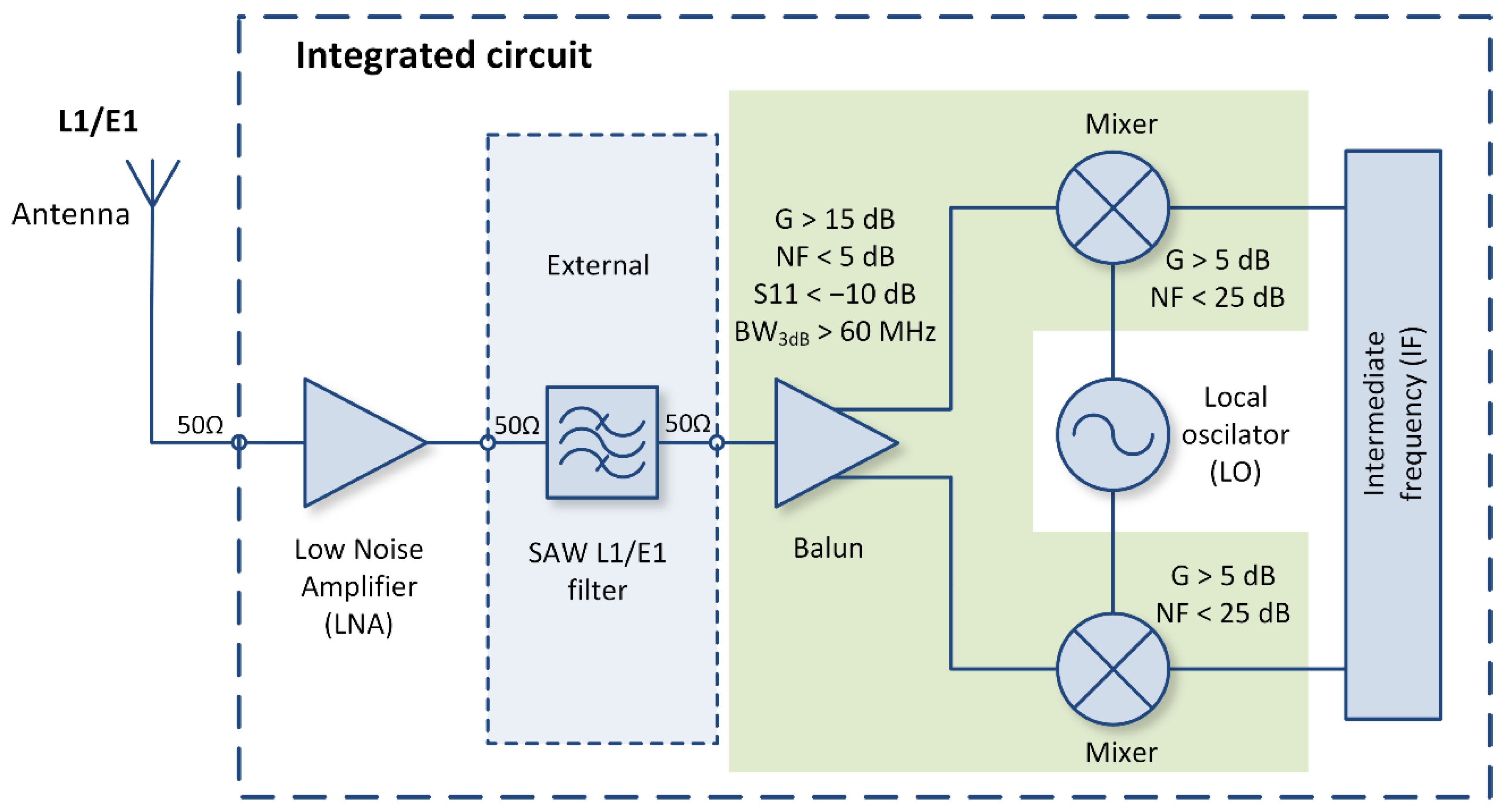
The balun and mixer presented below were used in a fully integrated dual-frequency (L1 and L5 bands) GNSS system on a chip (SoC) [30]. This article presents the narrowband balun and mixer implementation for the L1 band (center frequency at 1575.42 MHz ± 30 MHz). In the receiving path, the balun is between a low-noise amplifier (LNA) and a double-balanced Gilbert mixer, as shown in Figure 1. The balun circuit should be matched to 50 Ω on input. In the target chip, it is anticipated that the circuit will be able to operate in several configurations: with or without a SAW filter between the LNA (designed in the given IC) and the balun, or with an external LNA. The use of a balun is required due to the necessity of providing a differential radio frequency signal to the input of a double-balanced mixer.
Figure 1 also shows the desired parameters of the balun and mixer blocks. The balun should have a gain (G) higher than 15 dB and noise figure (NF) less than 5 dB. The input impedance matching for the balun should be better than −10 dB (S11 < −10 dB). The mixer should have a conversion gain higher than 5 dB and noise figure less than 25 dB. The balun is loaded directly by the mixer circuit. The mixer input represents a high impedance and a certain capacitance (Cgg of the mixer’s input transistor), which allows the balun to obtain good amplification.
The proposed balun circuit stands out from other solutions in that it makes it possible to obtain very good parameters in a simple way. Its main advantage is that it makes it easy to get a phase difference of 180 degrees between the output signals and the same amplitude for the output signals with the use of a properly connected coil with a tap. The second advantage of the circuit is the ease of obtaining impedance matching and noise matching at its input—as in a classic low-noise amplifier circuit. This matching is obtained by properly tuning the LC matching circuit. Staying on the subject of LNAs, the circuit makes it possible to achieve a very low noise figure, even below NF < 2 dB, of course with the optimization of the noise matching and appropriate polarization. This circuit also has several drawbacks. One of them is the need to use three coils, which is associated with a large occupied area. The advantage of the proposed balun is that it is narrowband, which makes it possible to selectively amplify the desired frequencies while filtering out interference signals. However, this circuit is not suitable for broadband solutions. In other research work, it was possible to obtain a 3 dB gain bandwidth with a width of 150 MHz and maximum gain of 25 dB. The circuit can find applications in all kinds of radio frequency transceiver systems with narrow, selective bands, and there is probably no better solution in these kinds of applications.
2. Design Considerations
2.1. Balun
A balun is a circuit for which the main function is to convert an unbalanced signal to a balanced signal. This circuit can provide signal amplification—an active circuit that draws current—or may introduce gain losses—a passive circuit that does not consume current. The balun circuit is very often used in radio frequency systems with frequency multipliers and mixers. If the noise requirements of the system are not too high (for example, NF > 2 is enough), a balun can be used as the first element of the radio path (after the antenna) and act as a low-noise amplifier. The key parameters that characterize the balun circuit are: the voltage gain/insertion loss, the amplitude and phase balance between balun outputs, the noise figure and the size of the device.
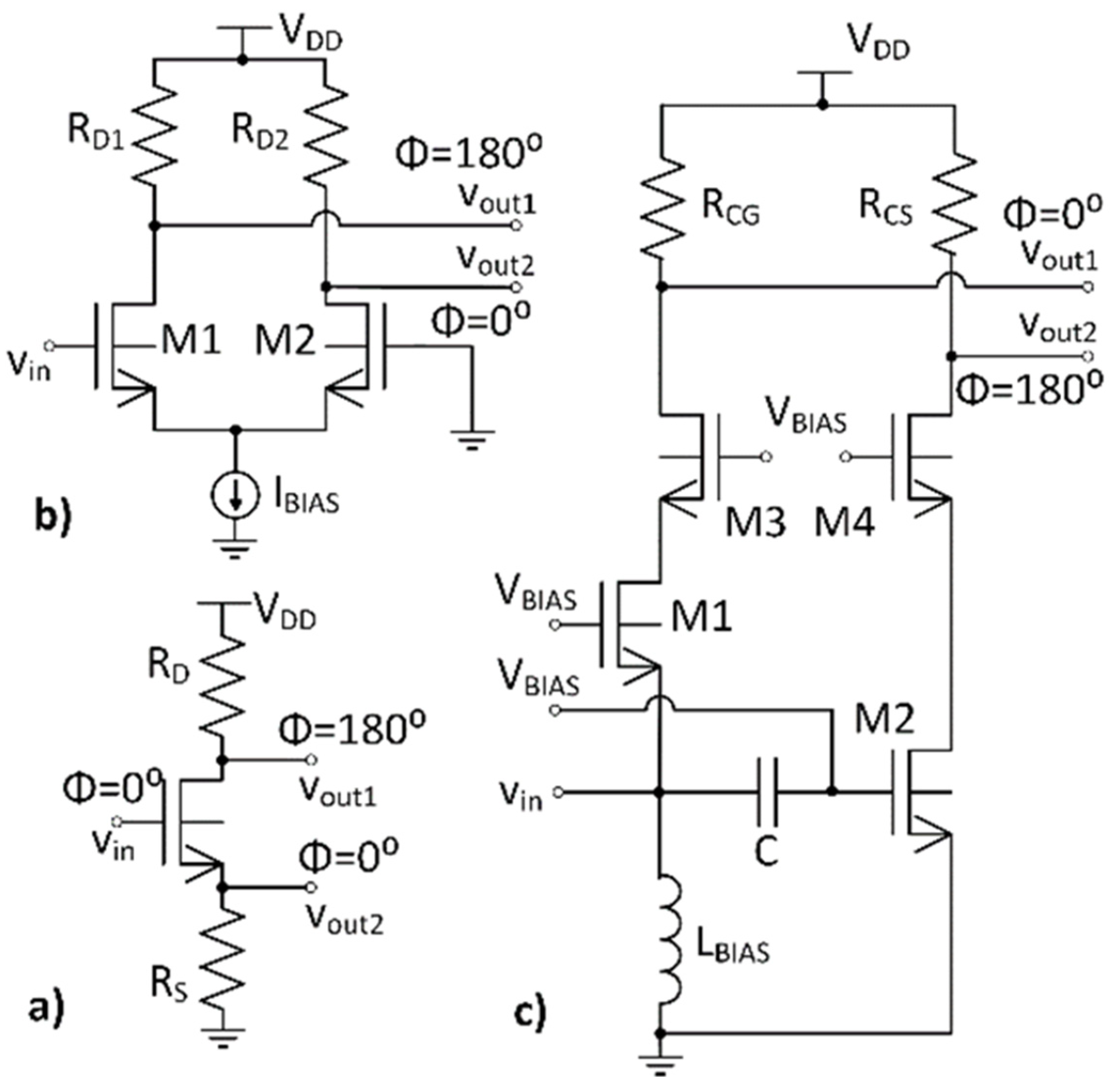
There are many active and passive circuits that have been designed to change an unbalanced signal into a differential one [21,22]. There are simple circuits, such as a single-transistor (Figure 2a) [24] or differential circuits (Figure 2b) [5,20], and more complex ones, such as common-gate–common-source baluns (Figure 2c) [1,2,3,4,6,13,16,17,19,21,22,23].
The first solution presented in Figure 2a is based on a single MOS transistor. Using the signal phase relationship between the transistor gate, drain and source, it can be seen that in an ideal case the alternating voltage at the drain is phase-shifted by 180° with respect to the input voltage at the gate. The alternating voltage at the source is in phase with the input voltage at the gate. In practice, two types of imperfections limit the use of this type of circuit. The first is the different signal amplifications between the transistor gate and transistor source, and the transistor gate and transistor drain. In order to compensate for different signal amplifications, the appropriate transistor dimensions have to be selected and suitable biasing circuits have to be designed. The second problem is the fact that the parasitic gate-source capacitance CGS and gate-drain capacitance CGD have different values. Different capacitances result in an incorrect phase difference (different from 180°) between the output signals. It should be emphasized that the phase error resulting from different parasitic capacitances depends on the frequency. Preliminary simulations of the considered circuit indicated a high noise figure.
The next considered solution is shown in Figure 2b. It is based on the classical differential amplifier. Transistors M1 and M2 are identical. An input signal is fed to the gate of M1 and the gate of M2 is connected to ground. In the ideal case, the alternating voltage at output vout1 is shifted by 180° with respect to the voltage at the M1 gate, and the voltage at output vout2 is in phase with the voltage at the M1 gate. The advantage of this implementation over the previous one is the ability to easily adjust the gains at both outputs. Preliminary simulations of this circuit indicated a high noise figure.
The main disadvantage of the first two circuits is the high noise figure; additionally, in the case of the first circuit, it is difficult to get the same gain at each output.
Therefore, it is a good idea to use a CG-CS stage (Figure 2c) [22]. This circuit consists of two amplification stages, an amplifier in the common-gate (CG) configuration and an amplifier in the common-source (CS) configuration. Both amplifying stages work in a cascode configuration, which makes it possible to achieve a high voltage gain through the RCS and RCG resistors. The role of the CG stage is to provide wideband input impedance matching and gain, while the CS stage provides the antiphase output signal. The noise level generated by the CG stage after obtaining input matching (gm = 1/RS) is of key importance for the entire circuit. With a properly designed CS stage, the noise of the CG stage can be reduced. The current noise of the M1 transistor generates voltage noise at the source resistance, the RCG resistor, and the amplitude of the latter is much higher and its phase is opposite to the input phase. The input noise voltage is amplified by the CS stage. The amplified noise is in phase with the voltage noise at the output of the CG amplification stage. Since the amplification of both stages is the same, this eliminates completely the noise at the differential output of the system. In order to achieve a low noise figure, the impedance of CS should be scaled down n times with respect to the impedance of CG. This circuit can simultaneously achieve noise cancelling, distortion cancelling and output balancing, as discussed in detail in [22].
However, there are problems with process corners, as well as voltage supply and temperature variation (PVT). As the circuit is not symmetric, each output signal is generated in a different way and the output phase difference can change by ±15° with PVT corners. The gain difference between the outputs is also strongly dependent on PVT corners.
2.2. Mixer
The mixer was implemented as a double-balanced active system (consuming current). An active circuit was selected to provide additional amplification of the signal in the receiver path. With the use of an active mixer, the noise figures of the next receiver stages have a smaller effect on the overall noise figure (this follows from the Friis formula—Equation (8)). A double-balanced circuit was chosen because it suppresses even and odd harmonic signals of the LO and RF input signals and provides good isolation between the mixer inputs and outputs.
The double-balanced Gilbert mixer circuit, often used in RF systems, was used in the implementation of the mixer. This circuit meets all the requirements mentioned above. Due to the use of a double-balanced circuit that requires an RF differential signal at the input, a balun circuit was present in the receiving path before the mixer.
3. Circuit Design
3.1. Balun
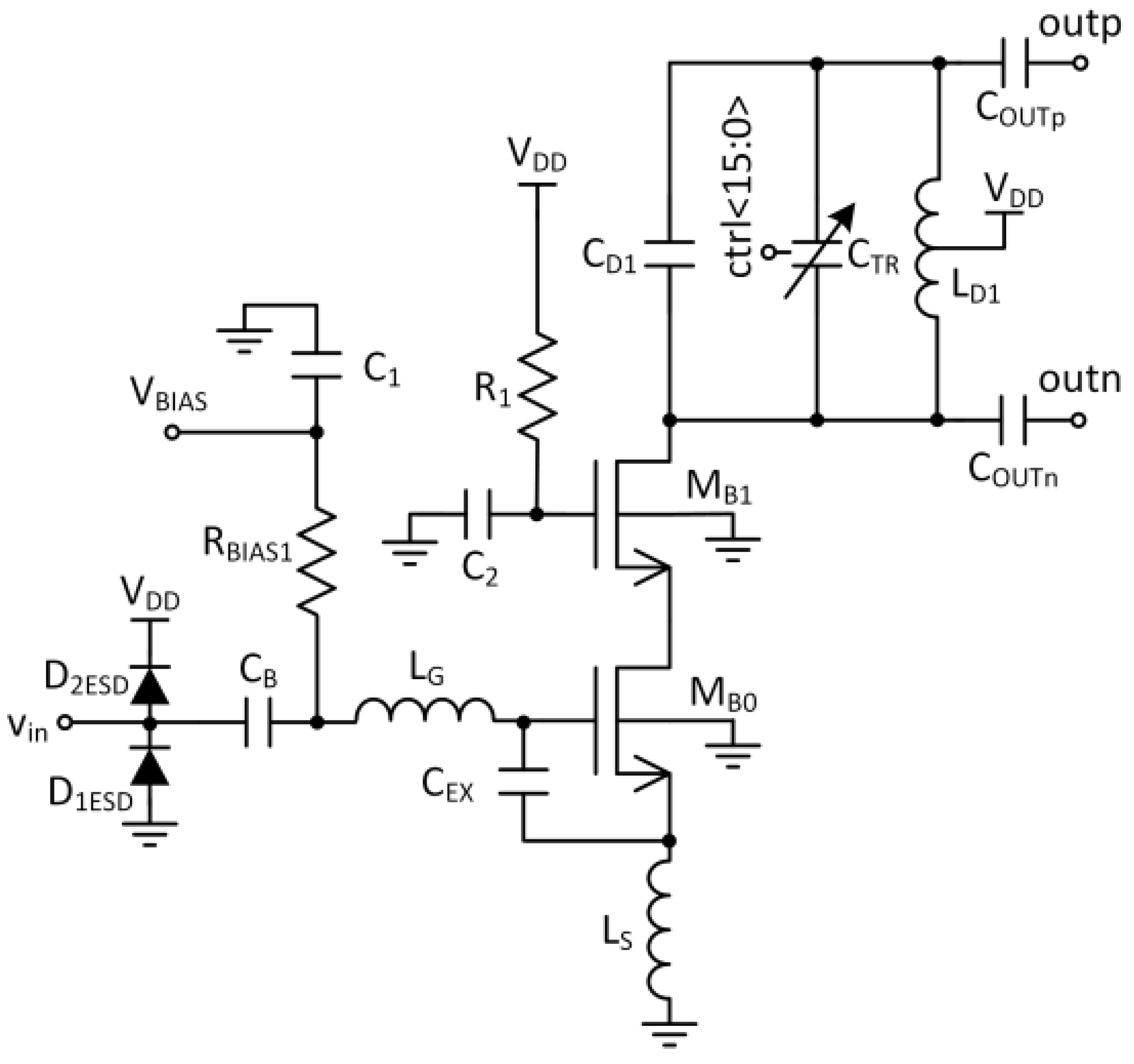
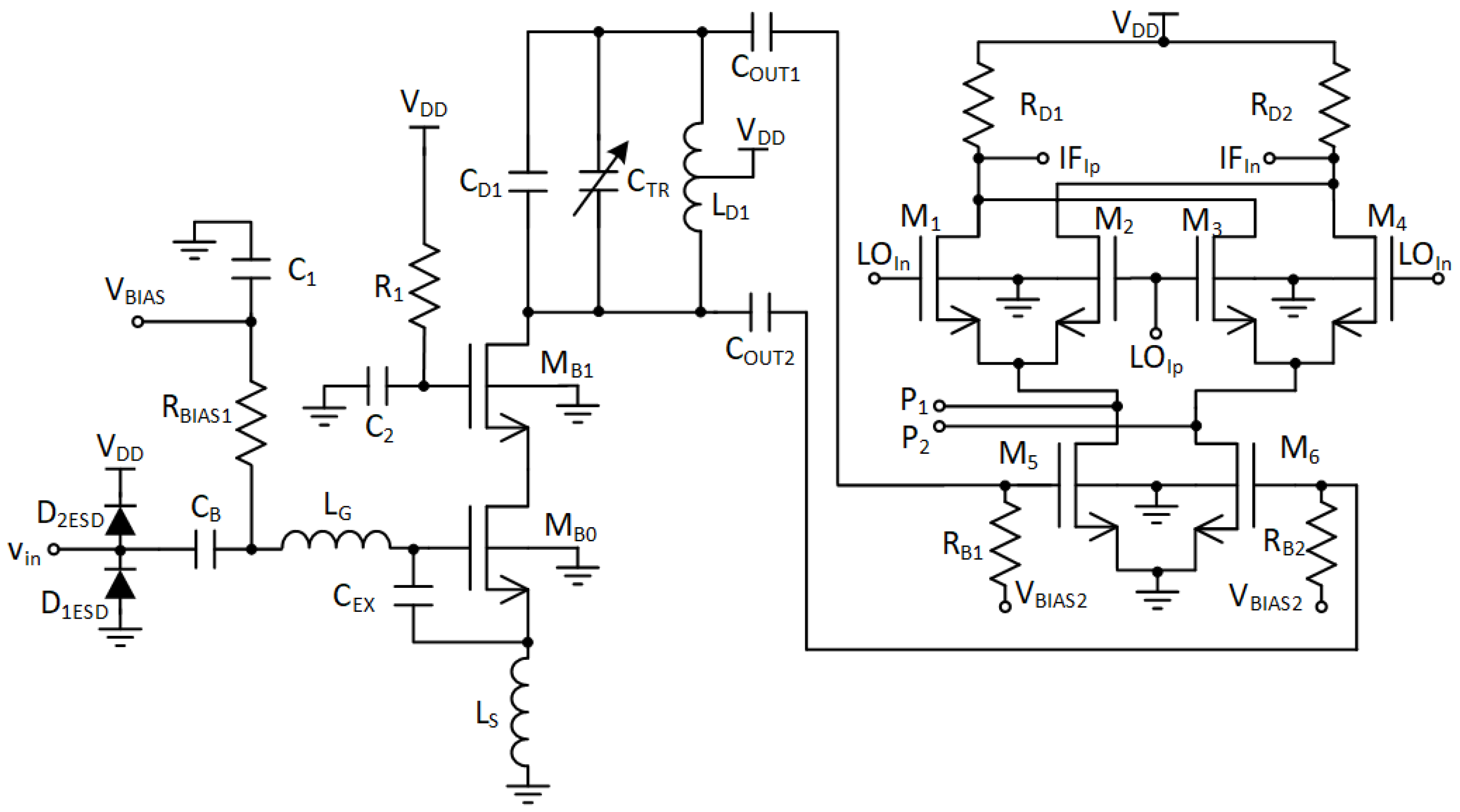
Figure 3 shows a new design for an active balun based on the classical CS degenerated cascode LNA. The main idea is to use a center-tapped inductor LD1 to generate two signals equal in amplitude and shifted in phase by 180° (differential signal). The layout of the inductor LD1 (shown in Figure 4) is symmetrical with respect to the center line bisecting the center terminal (CT).
The inductor LD1 with capacitor CD1 and capacitor tank CTR creates a resonance tank (acting as a bandpass filter). Moreover, it introduces the so-called shunt-peaking technique (using the resistance of the inductor as a serial resistor). This technique facilitates the optimization of the balun’s gain, bandwidth and center frequency without significantly increasing the power consumption.
Additionally, the proposed solution has a digitally controlled capacitor bank CTR (Figure 5). The switchable capacitor bank is designed to enable the post-production calibration of the balun. Calibration of the system parameters is needed because, under the influence of the technological process variation, the parameters of active and passive devices undergo unwanted changes and without calibration the designed circuits may have incorrect parameters (e.g., wrong center frequency of the amplified band).
The bank of switched capacitors proposed in Figure 5 allows correction of the amplified band (center frequency of the band). The capacitor bank consists of sixteen sections connected in parallel. Each section consists of a transistor MSW acting as a switch and capacitors CSW1 and CSW2 connected in series with it. Turning on the transistor MSW connects the capacitance section to the resonant circuit of the balun, which results in lowering of the resonance frequency and shifting of the central frequency of the amplified band towards lower frequencies. The center frequency of the balun can be calibrated in the 240 MHz range (±120 MHz from 1575.42 MHz) with a 16 MHz step.
The balun is matched to 50 Ω at the input because in the designed system it is possible to add (optionally) an external bandpass surface acoustic wave (SAW) filter between the LNA and the balun on a PCB. The input matching network of the balun consists of two inductors, LS and LG, and a capacitor CEX. The inductance LS controls the real part of the input impedance without adding noise. The LG coil determines a specific resonant frequency. The CEX capacitor facilitates simultaneous impedance and noise matching. Capacitor CB is used to cut off the DC component. The capacitance value of this capacitor should be large (a few pF) so that its impedance at the frequency of 1.575 GHz is as low as possible. The use of cascode makes it possible to achieve good isolation between the output and input and minimizes the capacitive Miller effect.
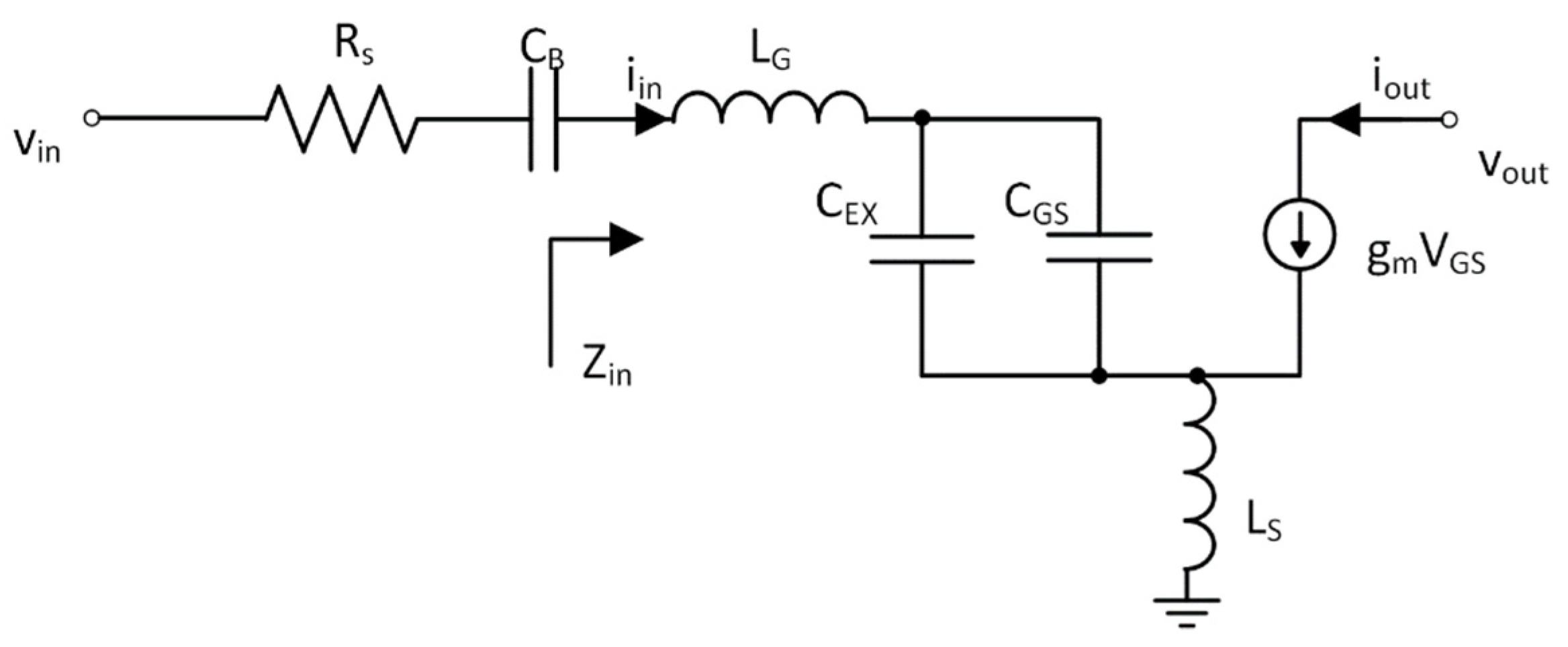
Formulas for calculating the input impedance were introduced based on the equivalent small signal circuit model (Figure 6).
The formulas describing the input voltage and output current are given below:
The input impedance is expressed by the following equation:
where LG and LS are inductances, CEX is additional capacitance for easier simultaneous noise and impedance matching, CGS is the cgs capacitance of the MB0 transistor and gm is the transconductance of the MB0 transistor.
The imaginary part of the input impedance is given by Equation (5). Then, Equations (6) and (7) for calculating LG and LS values that ensure impedance matching for Image (Zin) = 0 and Real (Zin) = RS = 50 Ω are derived as follows:
3.2. Mixer
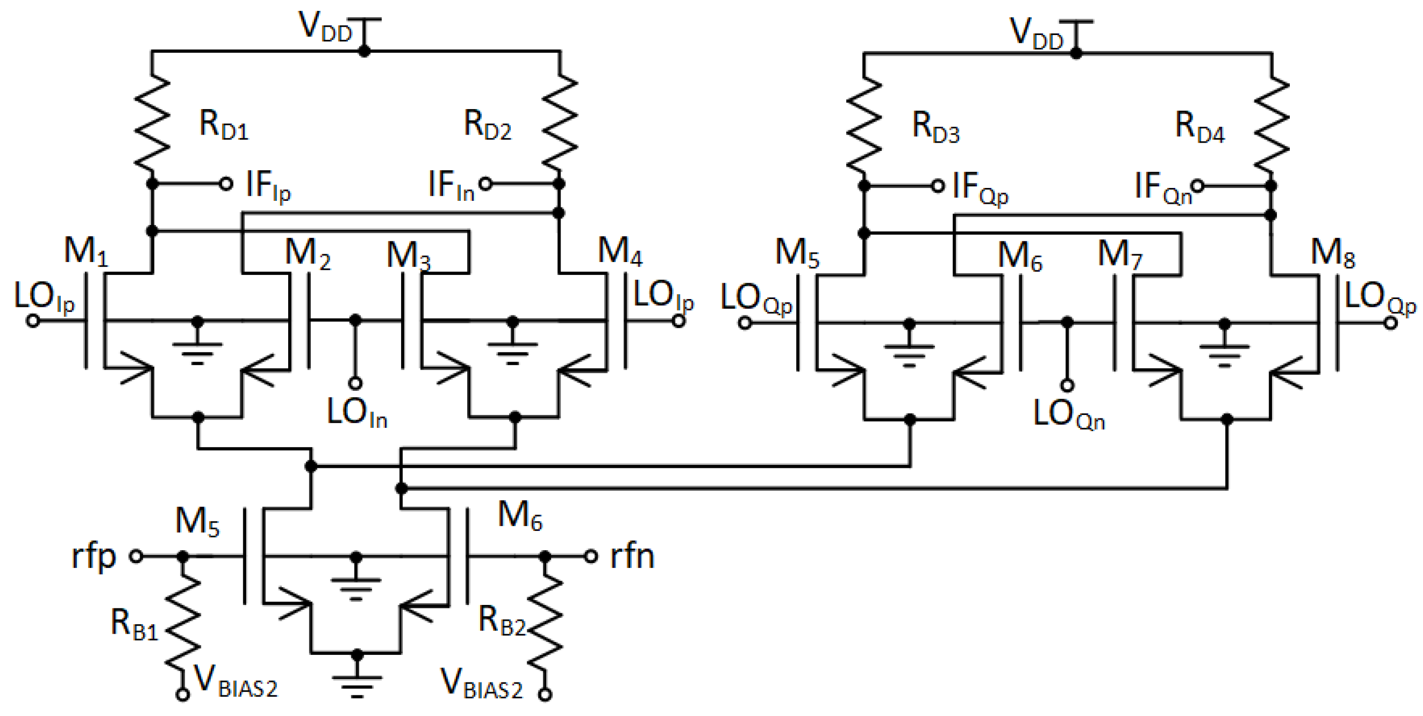
In the implementation of the receiver, a quadrature mixer was used (Figure 7)—two double-balanced Gilbert mixers the LO inputs of which were fed differential signals—Ip and In, and Qp and Qn—shifted in phase by 90°. Quadrature mixing allows for the complex demodulation of signals as represented by two orthogonal signals, IFI (IFIp, IFIn) and IFQ (IFQp, IFQn). Therefore the information from one sideband is not lost. In this study, only one mixer (in-phase) was examined with an active balun.
4. Results
Figure 8 shows the final version of the designed balun and mixer circuits presented and analyzed in this article. The following elements and their parasites were included in the balun simulation: bonding pad, ESD protection diodes and bond-wire connections between the IC and package. Taking all these elements into account made it possible to obtain good agreement between the measurements and simulations of the impedance matching of the input (S11 parameter) and the noise matching of the input (the value of the noise figure depends on the input noise matching). The section focused on the simulation presents detailed results of the balun and mixer post-layout simulations. The results are presented separately for each circuit, as well as for both circuits working together.
In the designed system, the signal behind the balun was not led outside the integrated circuit for measurement purposes. Therefore, the measurements section presents the results obtained from both circuits together after down-conversion. The signal input was the balun input and the output was the differential output of the mixer. In the balun and mixer measurements, at the output of the mixer, a measurement buffer (in the integrated circuit) with a gain of 1 was connected. The buffer was added in order to drive the output capacitance. The output of the measurement buffer was connected to the bonding pad to package. The signal from the mixer outputs enters the circuit (on a PCB), which converts the differential signal into an unbalanced one for measurement purposes. The measurement buffer does not introduce any changes to the simulation results; therefore, during the simulation, the mixer was loaded with a resistance of 50 kΩ and capacitance of 100 fF.
The output of the balun circuit was not accessible for measurement purposes because this would have required the design of a special output buffer with an output impedance of 50 Ω. Adding a measurement output at this point would have changed the operating conditions of the balun and mixer and degrade the parameters of both circuits.
The LO signal applied to the mixer input can be provided by an external generator or an internal digitally controlled oscillator (DCO). In measurements, the LO signal is generated internally by the DCO.
4.1. Simulation Environment
The circuit was designed with the use of Cadence software. The diagram was designed with the Schematic Editor L tool, the layout was designed with the Layout Suite XL tool and the simulations were performed with the ADE Explorer tool using the Spectre simulator. Extraction of parasitic elements was performed with a Quantus extractor with a field solver for greater accuracy.
The testbench of the circuit shown in Figure 8 consists of a 50 Ω signal source connected to the model of the connection between the package and bonding pad in the integrated circuit (IC). The bonding pad was directly connected to the input of the balun. At the output of the simplified testbench, the mixer was loaded with a capacitor of 100 fF and a resistor of 50 kΩ. The balun and mixer circuit loaded with the measurements buffer (in the IC) were also tested. Due to the fact that the connected measurement buffer did not change the parameters of the tested balun and mixer, it was decided to simulate the tested circuit with a simplified load (the simulations lasted for a shorter time).
The voltage supply of the system was 1.5 V and it was fed from a low dropout regulator (LDO) or an ideal voltage source. The reference current for both designed blocks was 4 µA and was supplied from a temperature-stable, voltage supply-stable and process corner-stable current mirror. Both designed circuits had local current mirrors to generate required polarizing currents and voltages.
The circuits were simulated in the temperature range of −40 °C to 85 °C for various corner cases of the technological process with a voltage supply fluctuation of ±10%.
4.2. Simulation Results
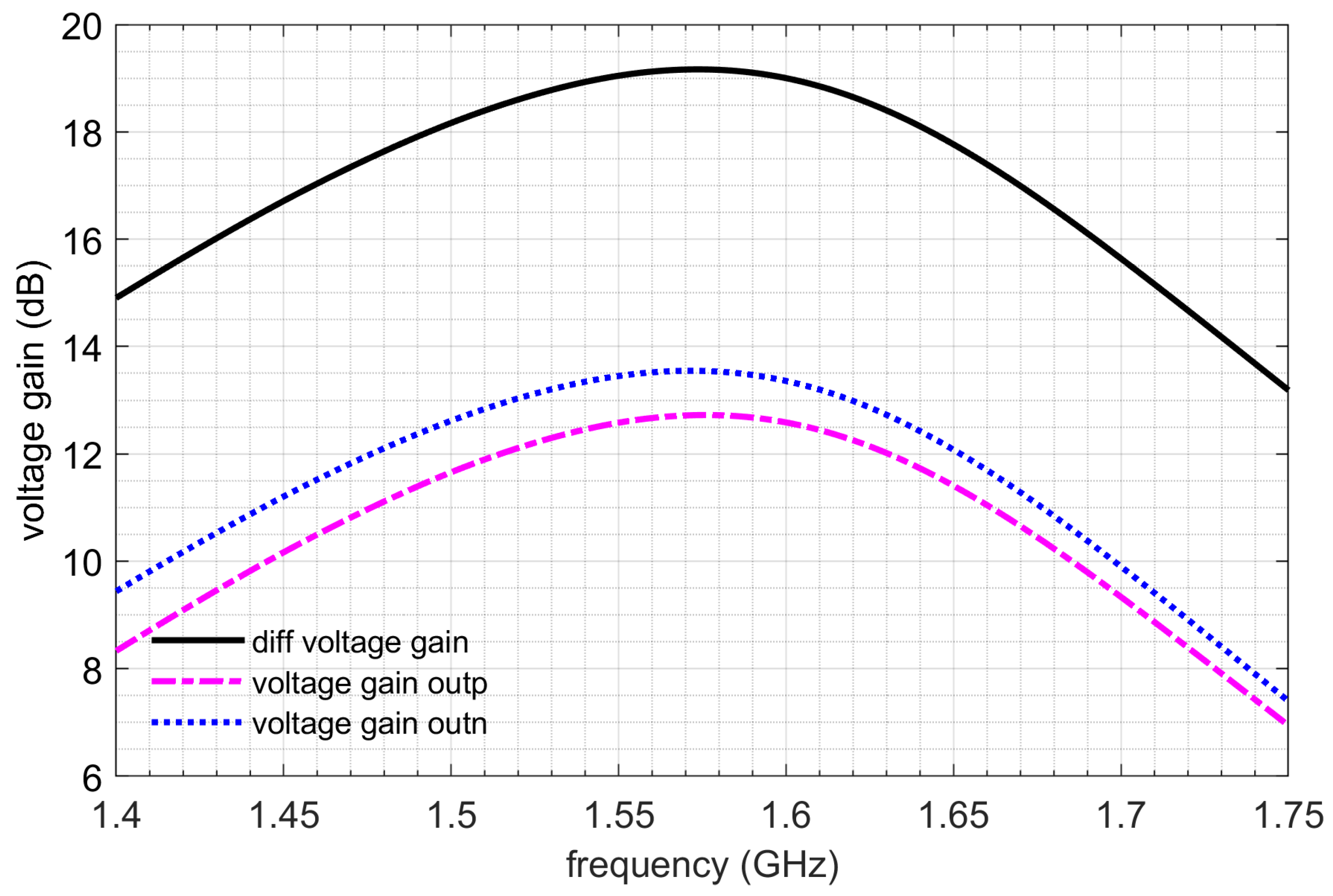
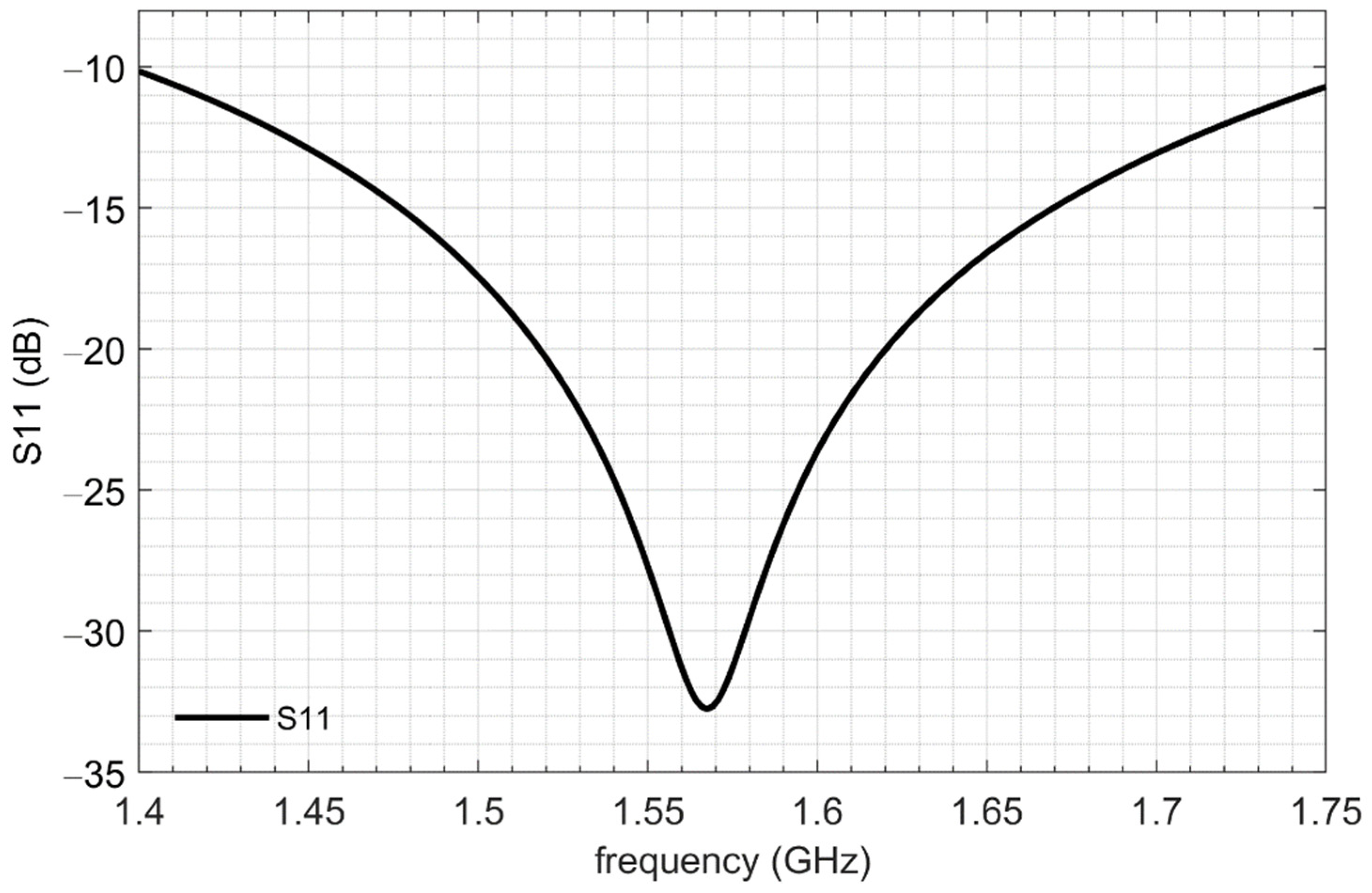
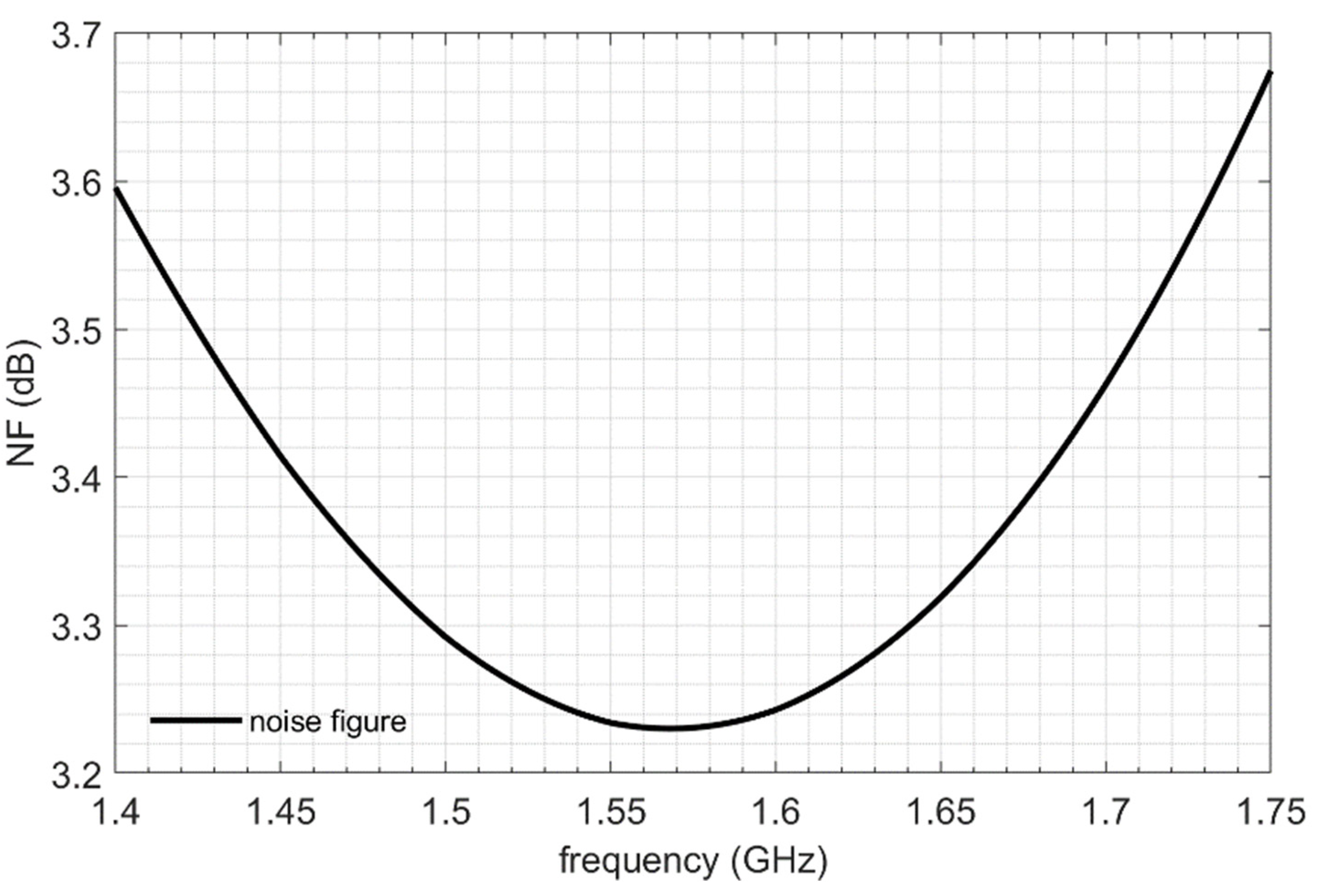
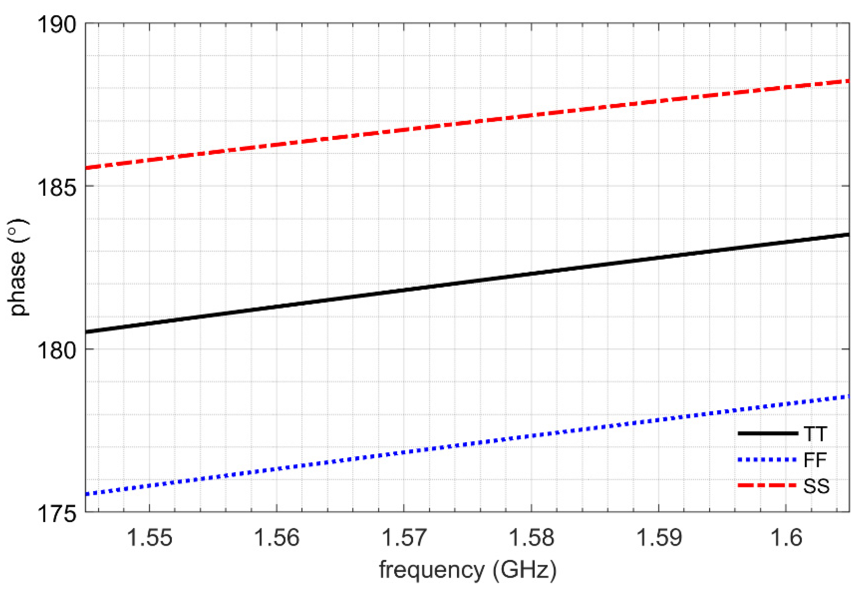
Figure 9, Figure 10, Figure 11 and Figure 12 show the main balun characteristics. The parameters of the balun at 1.57542 GHz were: voltage gain (GV) = 19.16 dB, S11 = −31.13 dB, NF = 3.23 dB, current consumption (IDD) = 1.5 mA, output phase difference = 182° and gain difference = 0.7 dB. The main advantage of the proposed circuit using a center-tapped inductor was that the phase shift between the outputs was equal to 180° with an accuracy of ±5° and the gain difference between balun outputs did not differ by more than 1.5 dB. This phase shift (Figure 12) and gain difference between the outputs was also well-preserved for all PVT corners (process corners: fast, typical, slow; temperature: from −40 °C to 105 °C; voltage supply: ±10%). The characteristics in Figure 9, Figure 10 and Figure 11 show the results of the post-layout simulation in a typical process corner: 27 °C and nominal voltage supply 1.5 V.
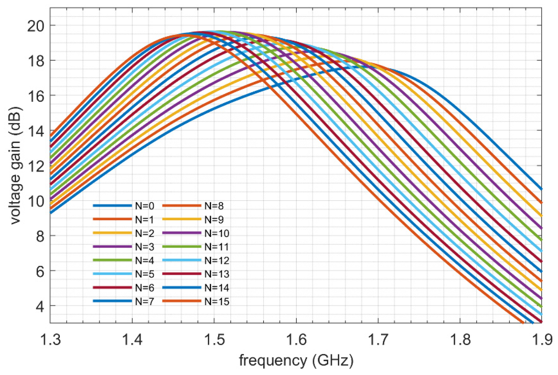
Figure 13 shows the voltage gain characteristics for various settings (N) of the switched capacitor bank CTR. For the nominal case of the technological process corner, six sections of the capacitor bank (N = 6) were connected. With this setting, the center frequency of the band is 1.575 GHz. The center frequency of the balun could be calibrated in the 240 MHz range with a 16 MHz step, as shown in Figure 13.
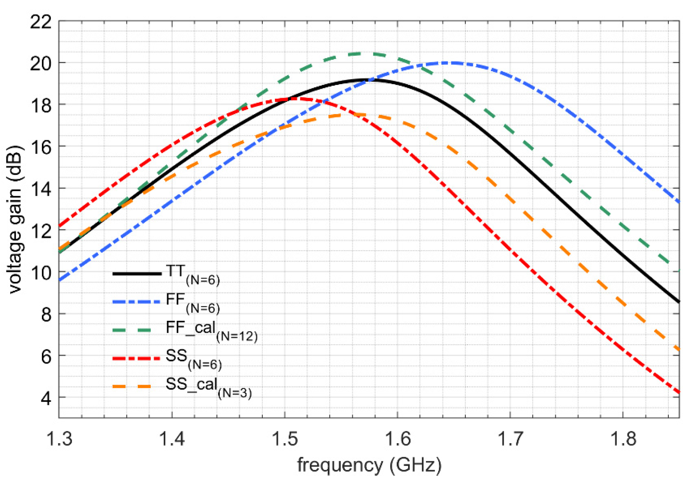
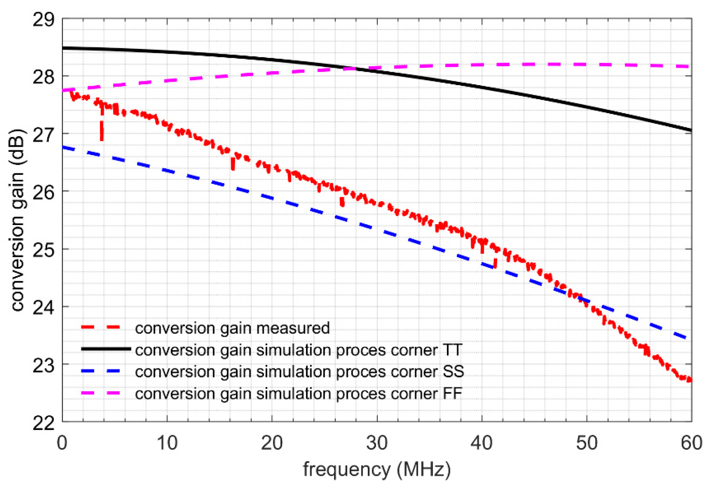
Figure 14 shows the application and operation of the calibration system. The TT characteristics show a balun voltage gain for the nominal case of the technological process and the nominal configuration of the switched capacitor bank (N = 6). The SS and FF characteristics show a situation where the parameters of the circuit (voltage gain) are under the influence of the technological process variation (at the nominal configuration of the switched capacitor bank). SS means the corner case where the technological process is slow: slow transistors, high capacitances and high resistances. FF means the corner case where the technological process is fast: fast transistors, low capacitances and low resistances.
As can be seen in Figure 14, the characteristics corresponding to the slow and fast process corners were significantly shifted in frequency. The FF characteristics were shifted by 75 MHz towards higher frequencies, and the SS characteristics were shifted toward lower frequencies by 75 MHz. To compensate for this shift, the circuit can be calibrated using the switched capacitor bank (FF_cal and SS_cal characteristics in Figure 14). In order to calibrate the circuit for the FF corner case, an additional six sections of the capacitor bank (N = 12) were connected, which resulted in the FF_cal characteristic. In the SS corner case, four capacitor bank sections (N = 3) were disconnected, which led to the calibrated SS_cal characteristics of the balun voltage gain.
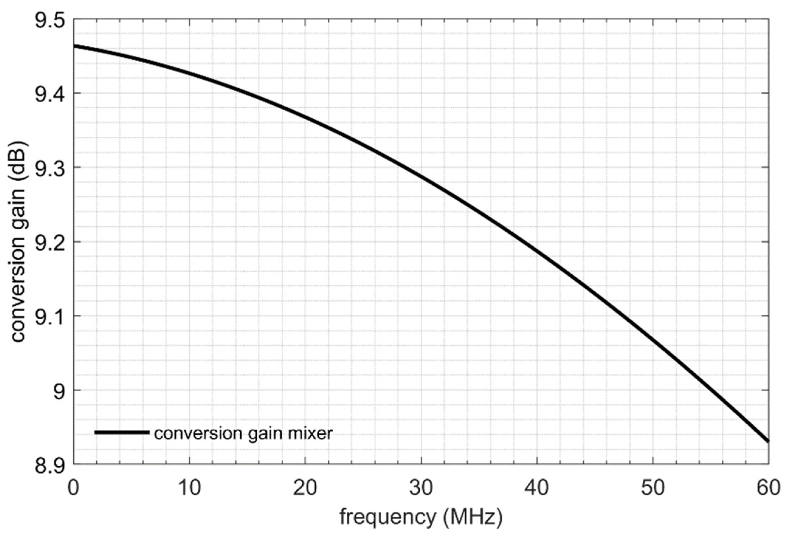
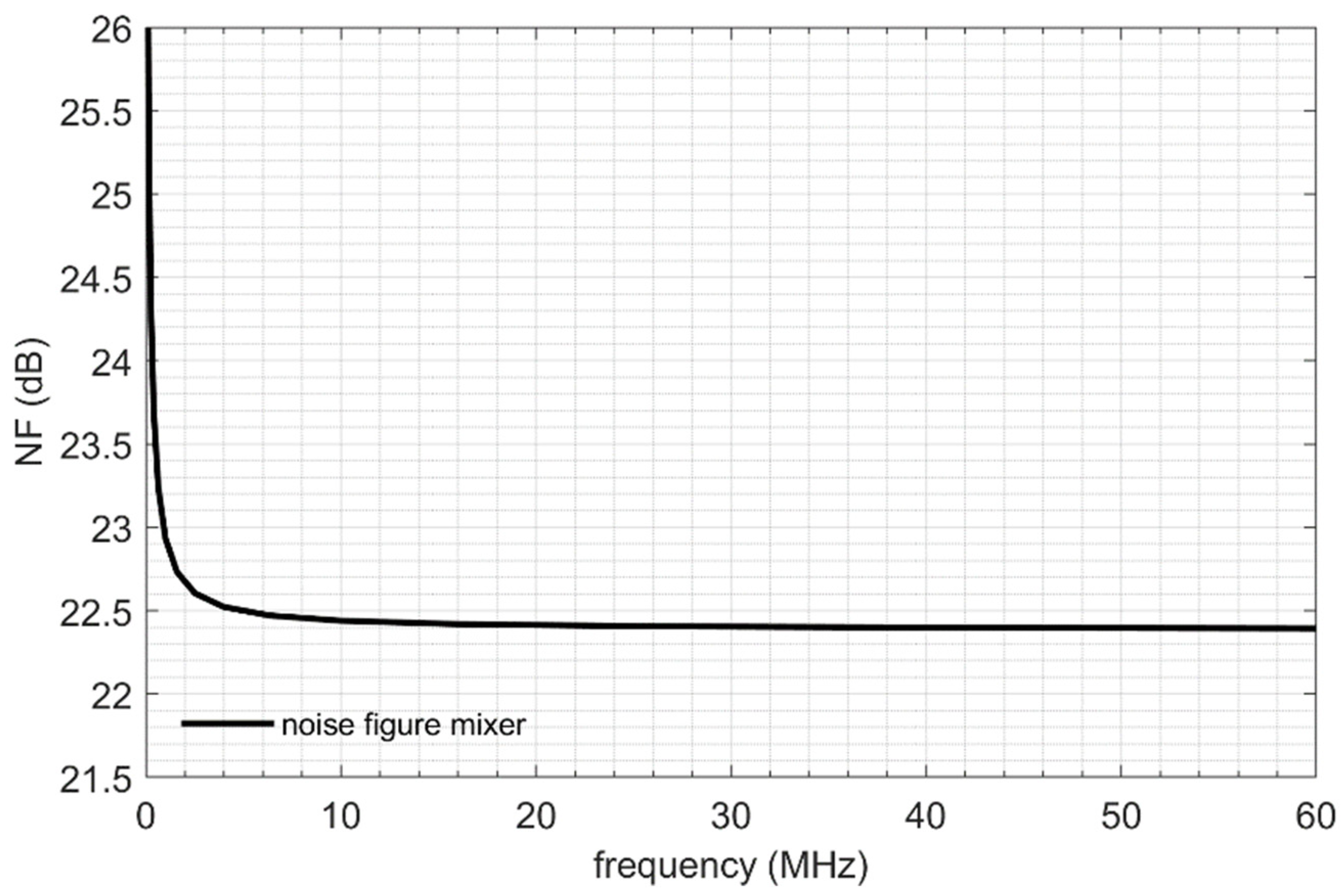
Figure 15 shows the conversion gain and Figure 16 shows the double sideband (dsb) noise figure characteristics of the mixer. Both parameters met the requirements. As we can see, the conversion gain in the bandwidth of 30 MHz (from 0 to 30 MHz) dropped by about 0.2 dB. The noise figure was around 22.5 dB.
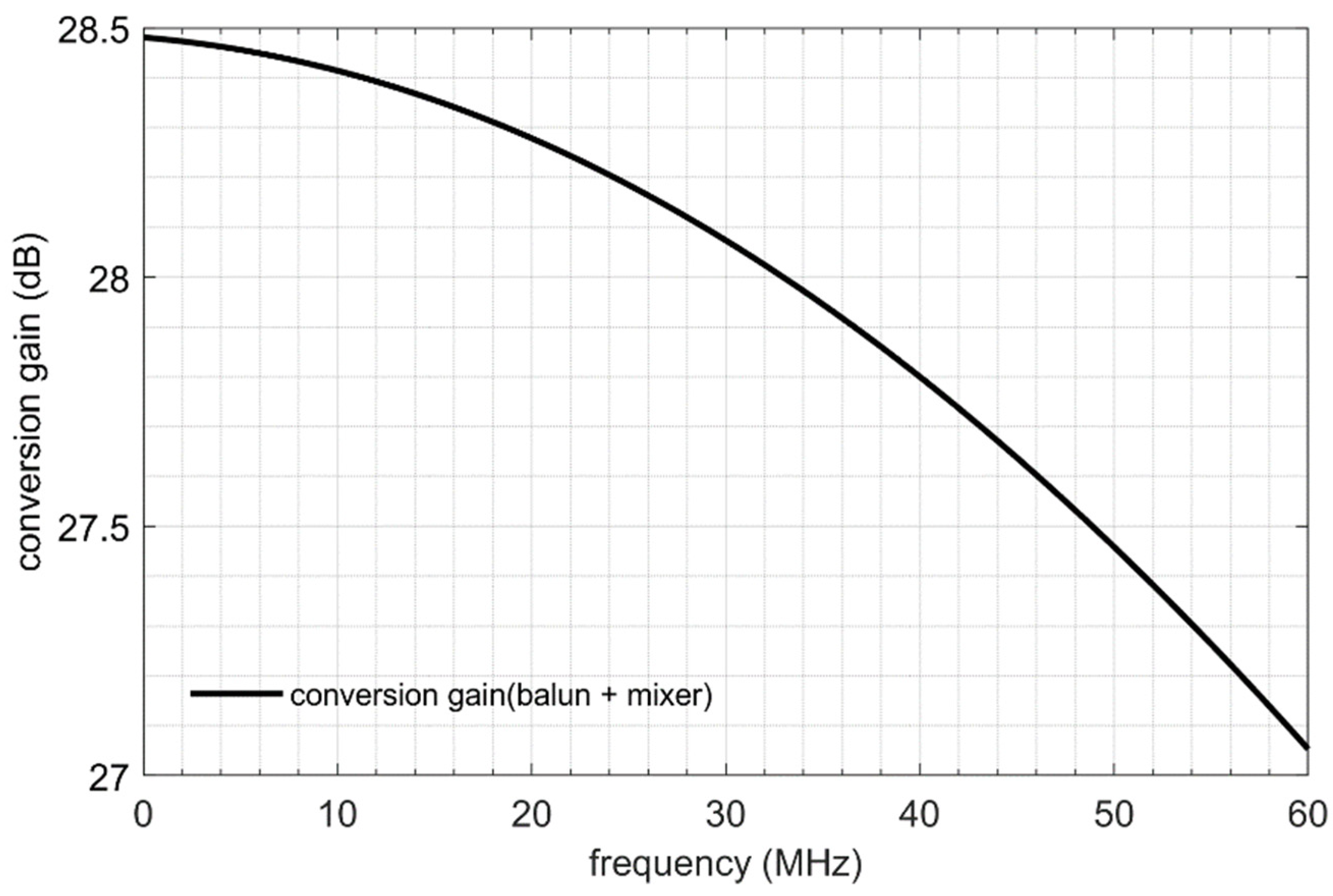
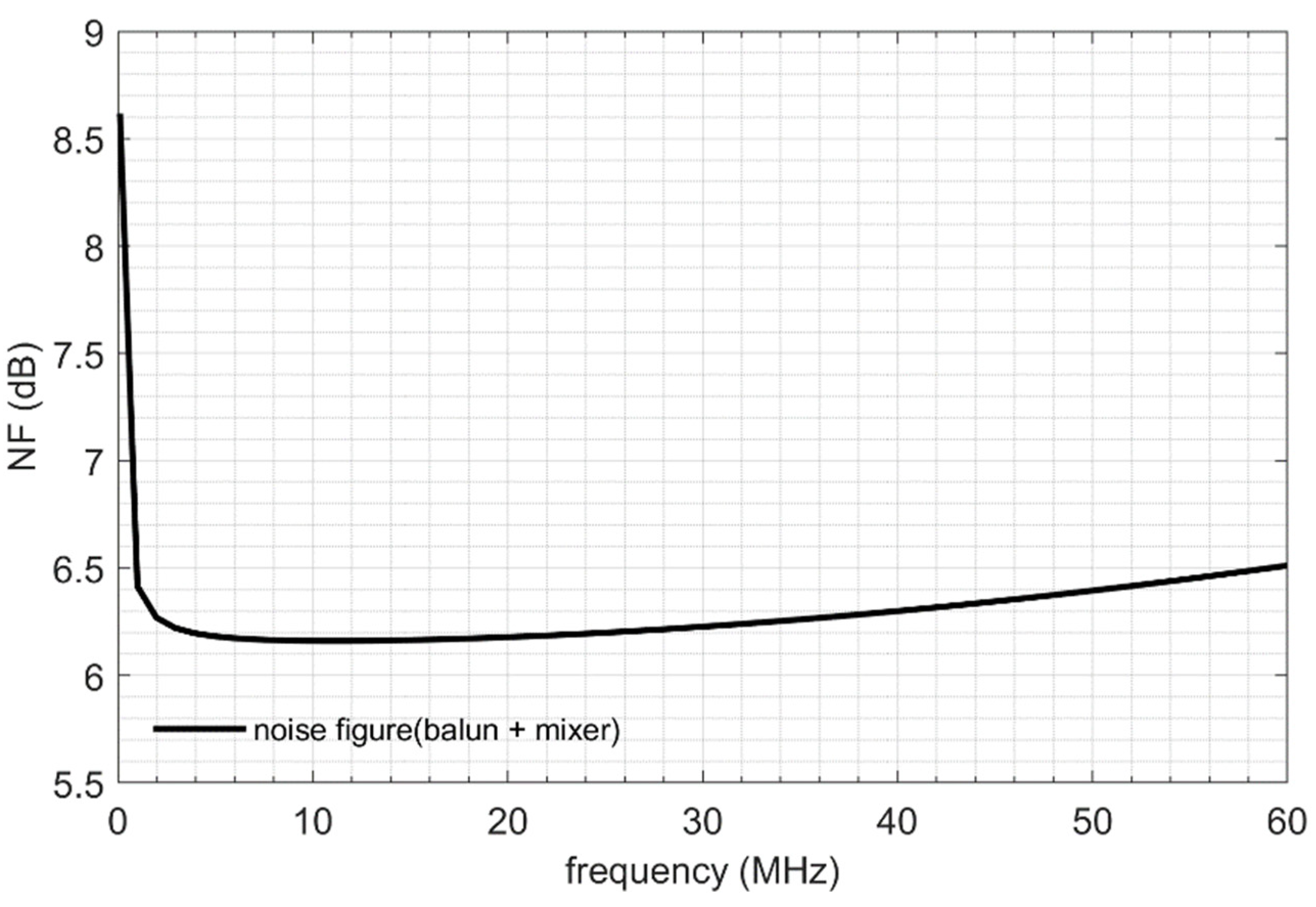
Figure 17 shows the total conversion gain and Figure 18 shows the dsb noise figure of the balun and mixer. As we can see, the conversion gain in the bandwidth of 30 MHz dropped by about 0.5 dB. A slightly greater decrease in conversion gain in the bandwidth (compared to mixer) resulted from the summation of the balun gain curve and mixer conversion gain curve. The conversion gain decrease in the band was due to the shape of the balun gain curve, which decreased in the band (1.575 GHz ± 30 MHz) by 0.3 dB. The maximum noise figure in the band was NF = 6.4 dB with the omission of 1/f noise which was stronger at low frequencies (<1 MHz)—later, this noise will be filtered out in the receiving path.
4.3. Measurements
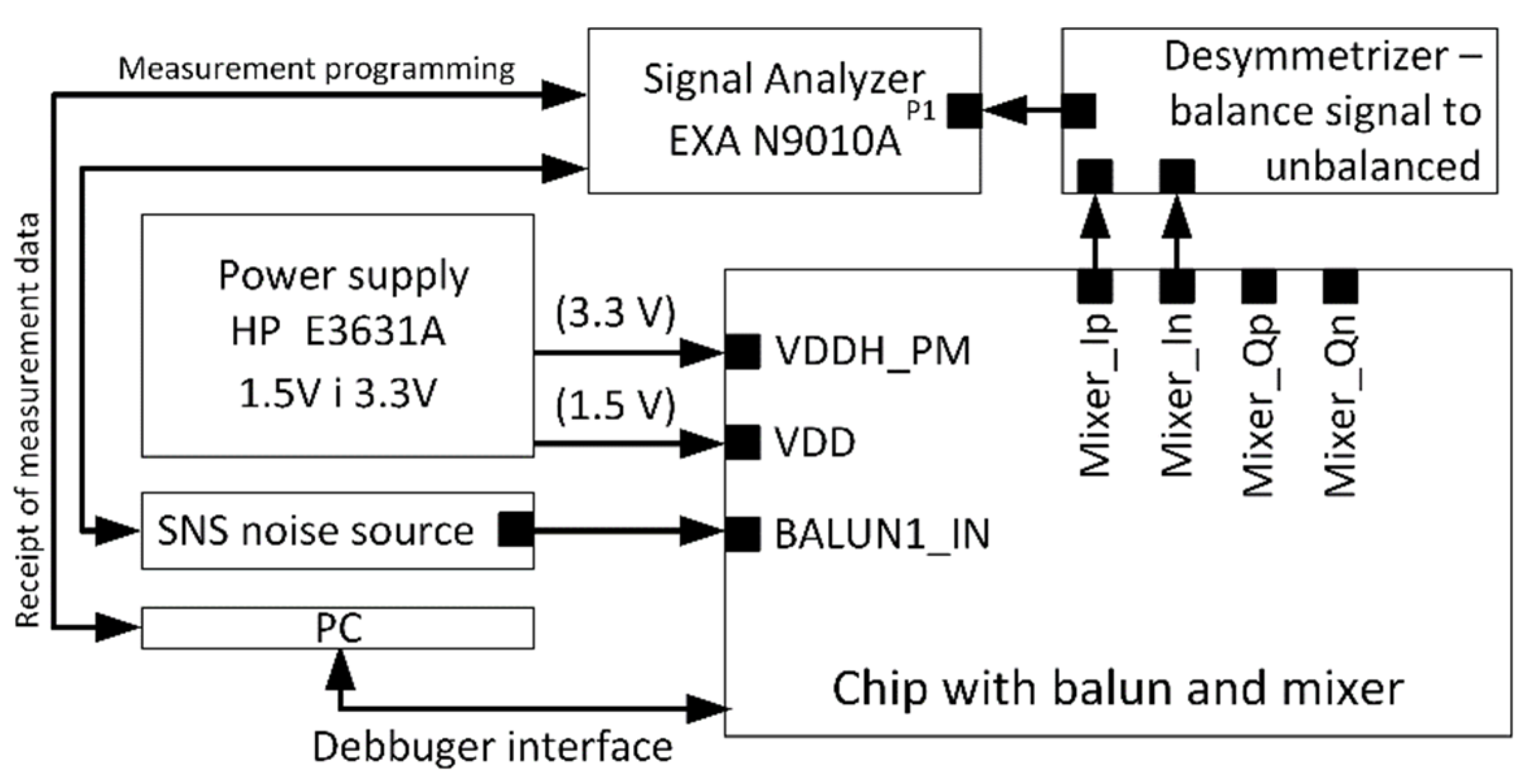
The environment for measuring the balun and mixer parameters is presented below in Figure 19 and Figure 20. It consisted of an HP E3631A laboratory power supply providing supply voltage to the in-chip reference current source for the balun and mixer circuits. The first of the measurement systems shown in Figure 19 was used to measure the noise figure and conversion gain.
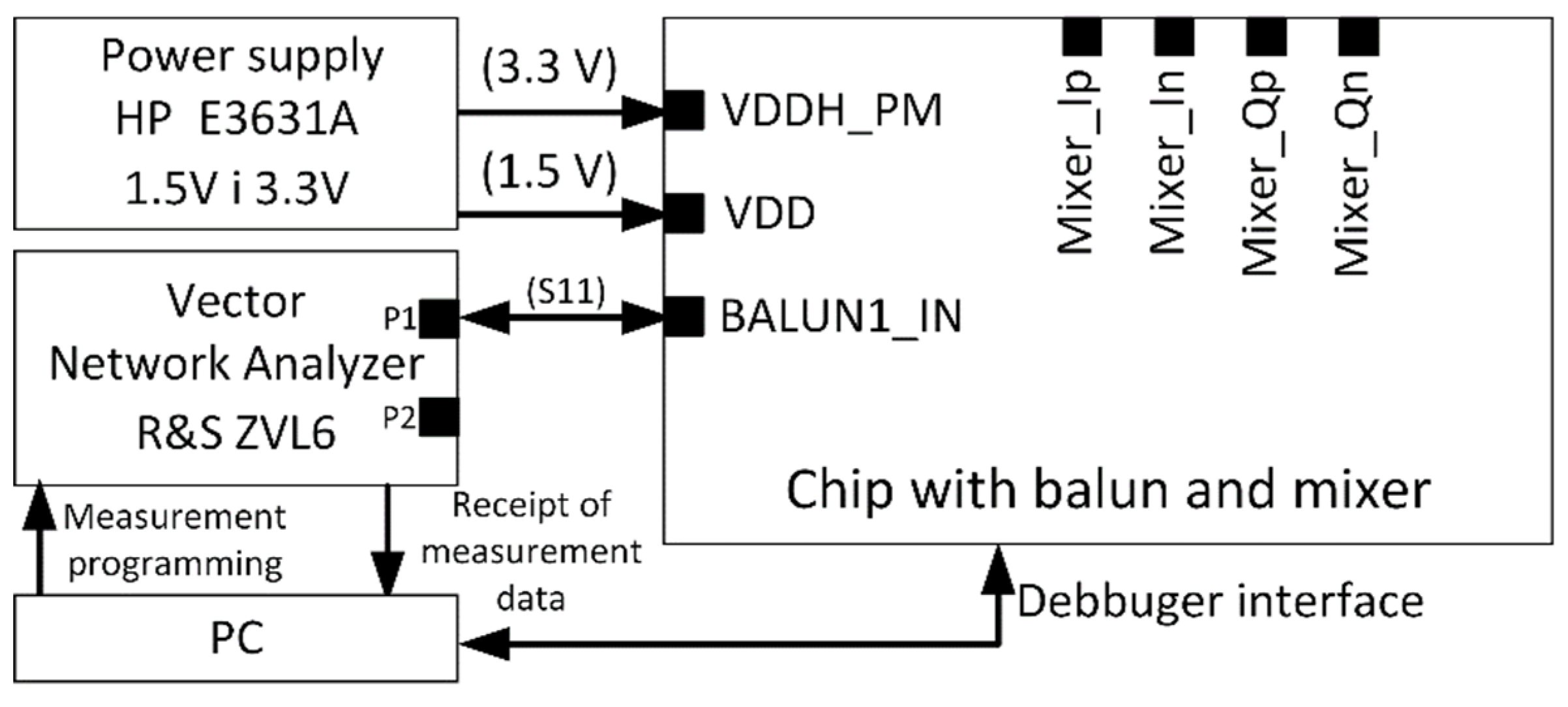
The second measurement system shown in Figure 20 was used to measure the input impedance matching (S11 parameter).
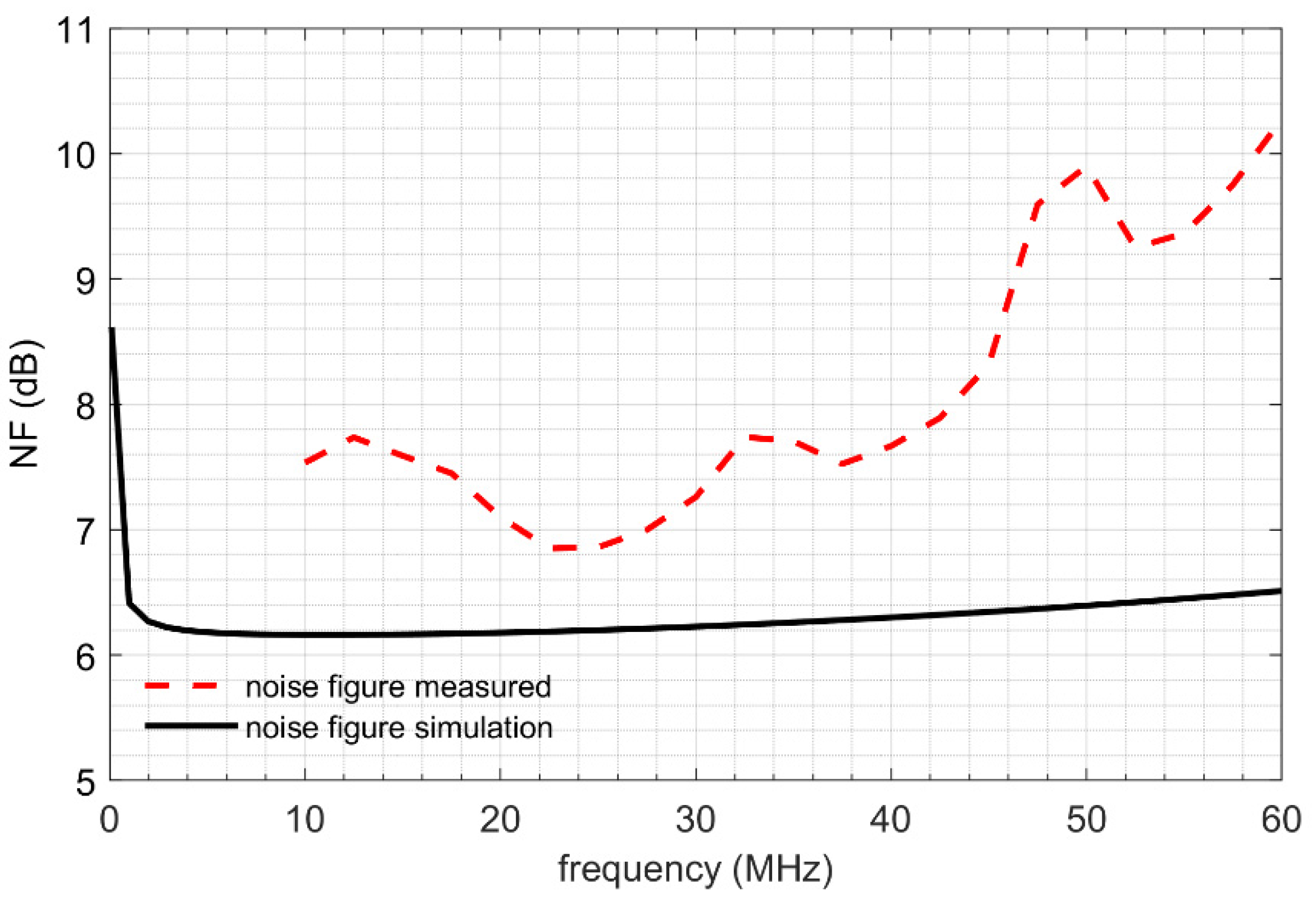
Figure 21, Figure 22 and Figure 23 below compare the experimental and simulation results. Figure 21 shows a comparison of the simulated and measured noise figure. The noise figure obtained as a result of the measurement had a greater value than that obtained in the simulation. This may have been due to, e.g., the decrease in the balun gain (Figure 22), which very much determines the total noise figure.
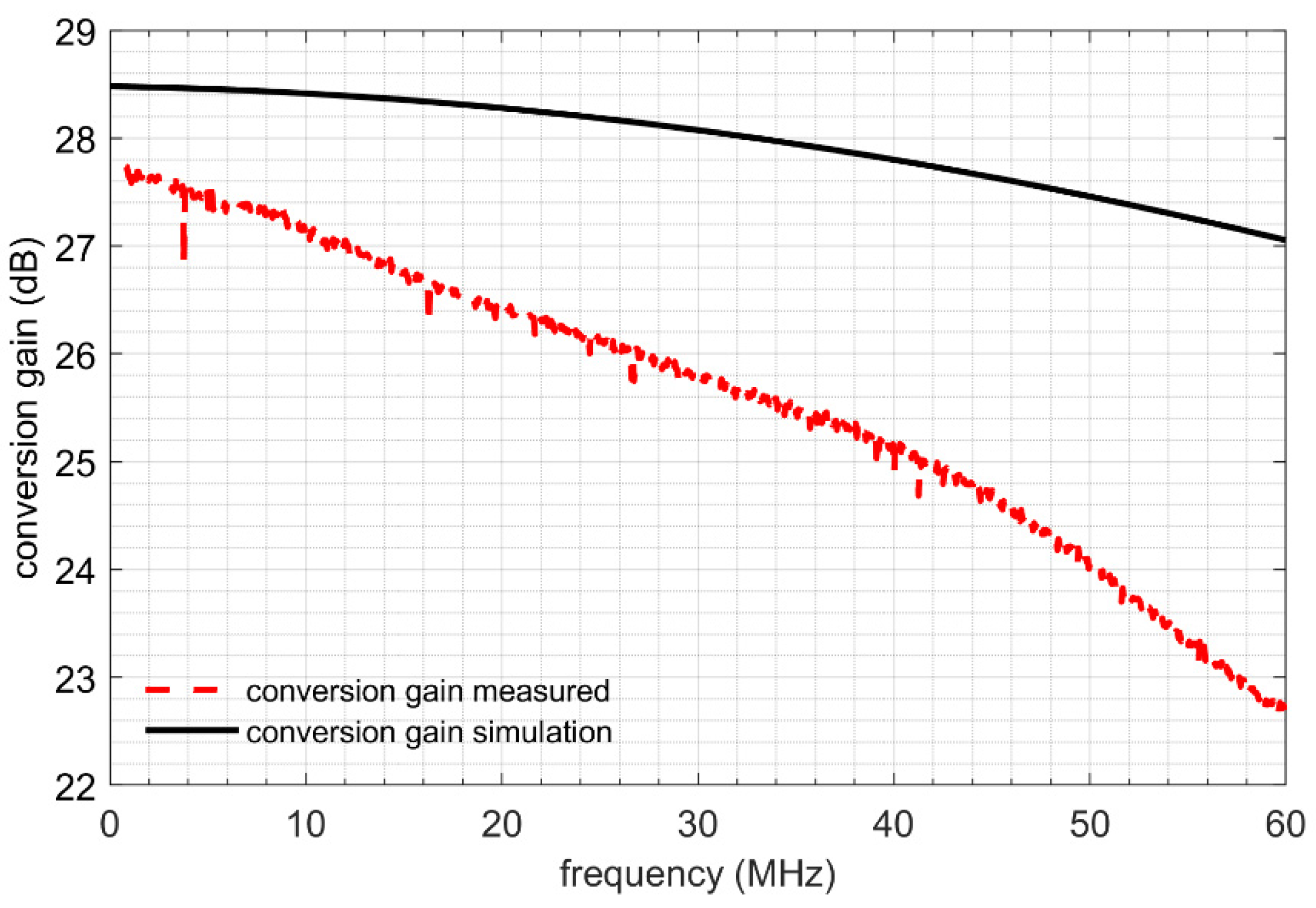
The gain conversion characteristics obtained as a result of the post-layout simulations and measurements are compared in Figure 22. The measured conversion gain decreased by approximately 0.7 dB (near 0 Hz). In addition to the decrease in gain, the nature of the gain curve changed—it descended faster. The simulated conversion gain at the 30 MHz was 28 dB, while the measured one was 25.8 dB. The change in the conversion gain curve could have been caused by the output circuits used for the measurement and/or a small band shift of the balun resulting from the dispersion of the parameters of the technological process. One of the output measurement circuits was a buffer (in the integrated circuit) designed to drive a large capacitance and the second one (on a PCB) was intended to convert the symmetrical signal into an unbalanced one. These two circuits at the balun and mixer outputs were designed only for measurement purposes.
When investigating what the cause of the difference between the measurement and the simulation of conversion gain was, the influence of the technological process dispersion on the gain conversion characteristics was verified by means of simulations. Figure 23 shows the characteristics of the gain conversion resulting from the measurement (same as Figure 22) and simulation for the typical case (same as Figure 22) and the corner cases SS and FF. As can be seen, the measurement result was within the limits of the possible dispersion of the technological process. By analyzing the measured characteristic of the gain conversion, it can be concluded that the center frequency of the balun amplification band shifted towards the lower frequencies—which may indicate that in the production process we came closer to the SS case, where larger capacitances are modeled during the simulation.
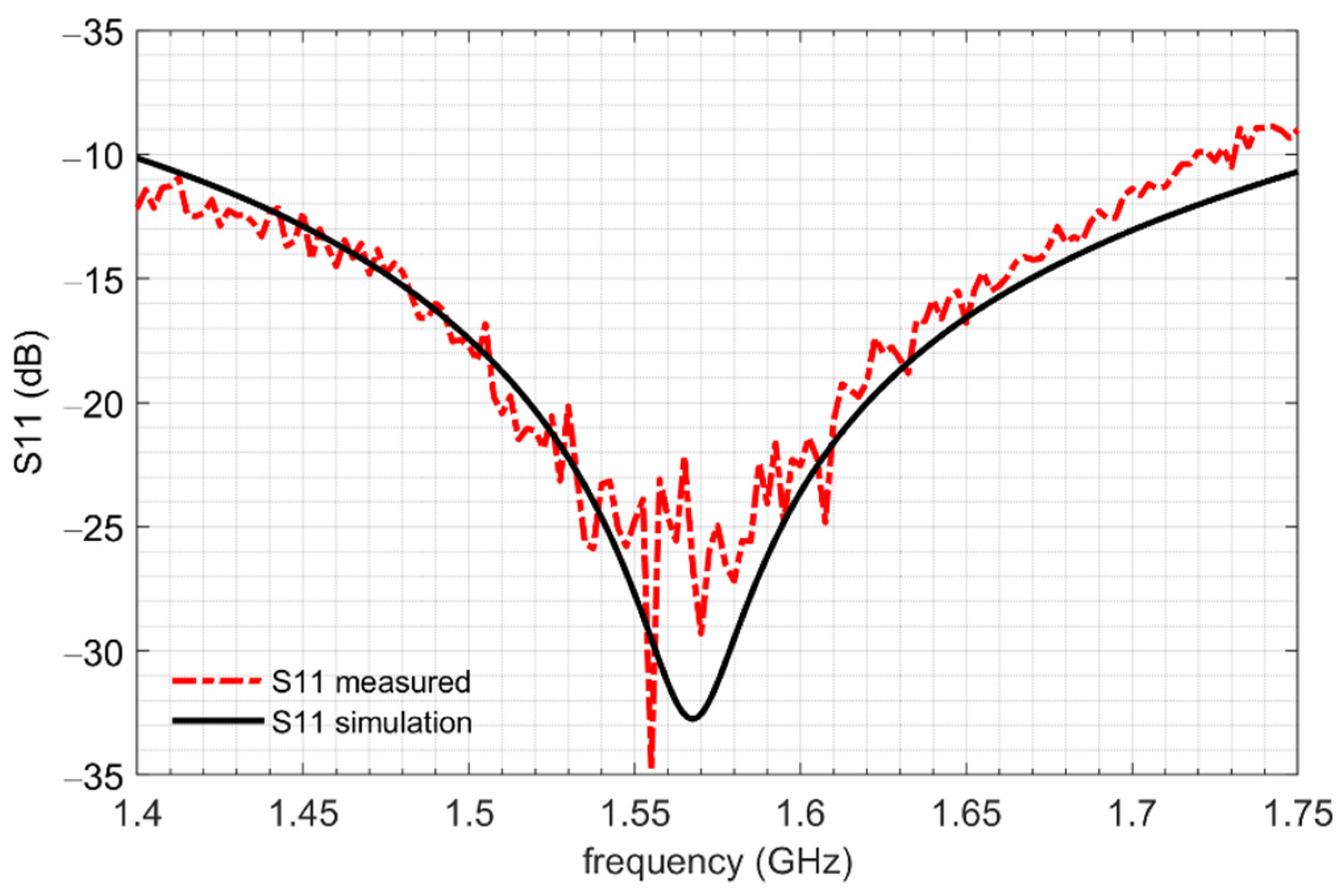
Figure 24 compares the results of the simulation and measurement of the input impedance matching (S11 parameter). The measured values of S11 agreed well with the simulation results.
As no studies on narrowband baluns and mixer systems were found in the literature (one can find many papers on broadband solutions), only the parameters of the designed balun were compared with other implementations found in the literature. The balun gain was estimated from the measurement results of the balun and mixer systems together, because the measurements were made only for the balun and mixer working together. It was assumed that the decrease in the balun gain (Figure 22) caused an increase in the total noise figure, as seen in Figure 21, which was consistent with the calculation using the Friis formula (Equation (8)). FN (noise factor) and Gn (gain) are given as linear factors (not in decibels) of subsequent elements of the receiving path.
The total noise figure is the noise factor given in decibels:
It was estimated that the balun gain was reduced to 18 dB and the mixer noise figure increased to 24 dB, which would give a noise figure increase to about 7.7 dB in the band of interest (30 MHz).
The parameters of the balun are summarized and compared with other published CMOS baluns [3,4,22,23] in Table 1. It can be seen that the proposed balun achieved the lowest power dissipation and had the best impedance input matching compared to other results. In this application, the noise figure of 3.23 dB was sufficient because the balun was the second element of the receiver—it was located behind the low noise amplifier. The total noise figure of the receiver in this case was determined by the noise figure of the low noise amplifier and its gain. It should be emphasized that the applied architecture of the active balun makes it possible to achieve a very low noise figure with a sufficiently high current and noise matching optimization. In this implementation, noise minimization was not carried out because low power consumption was more important.
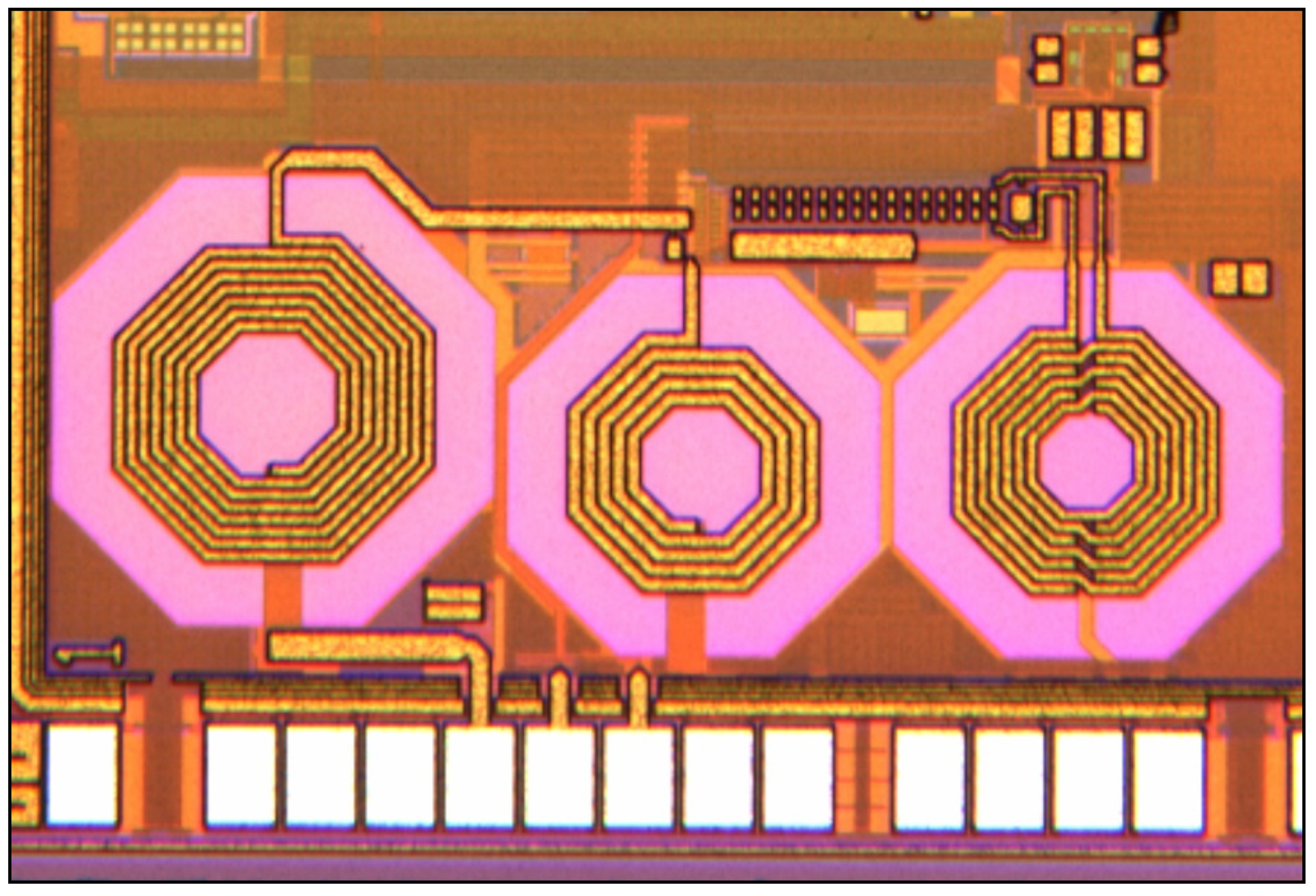
Balun and mixer microphotography is shown in Figure 25. The layout dimensions of the designed balun and mixer were 1012 µm × 592 µm.
5. Conclusions
The proposed active balun performs with triple functionality in the GNSS RF front end. It ensures a 50 Ω input match, provides additional signal amplification and delivers a differential RF signal to the down-conversion mixer. The phase shift between the balun outputs is close to 180° and the gain of each output is almost identical. This is possible due to the use of a center-tapped symmetric inductor as an element generating the differential signal. The phase and gain variations between outputs do not exceed 5° and 1.5 dB, respectively, across the simulated PVT corners. The use of an active balun made it possible to reduce the noise requirements for the mixer. The estimated parameters of the balun, based on post-layout simulations and measurements of the total conversion gain and total noise figure of the balun and mixer, were: GV = 18 dB, NF = 3.23 dB, S11 = −22 dB, IDD = 1.5 mA.
The proposed Gilbert double-balanced mixer system performs with double functionality in the GNSS RF front end. The main task is to convert the RF signal into an intermediate frequency signal. The second task is to provide additional signal amplification in the receiving path. The estimated parameters of the mixer, based on post-layout simulations and measurements of the total conversion gain and total noise figure of the balun and mixer, were: conversion gain GC = 9.3 dB, NF = 24 dB and IDD = 0.66 mA.
The measured total noise figure and total conversion gain were, respectively: NF = 7.7 dB and GC = 25.8 dB in the band of interest. The measured current consumption was IDD = 2.24 mA. The designed system meets the specification.
Author Contributions
The work presented in this paper was a collaboration of all the authors. RF and analog design, visualization, writing, D.P.; conceptualization, validation, T.B.; supervision, writing—review and editing, project administration, funding acquisition, W.A.P. All authors have read and agreed to the published version of the manuscript.
Funding
This work was supported in part by the Polish National Centre for Research and Development under project no. POIR.04.01.04-00-0101/16.
Data Availability Statement
The data presented in this study are available on request from the corresponding author. The data are not publicly available due to the ongoing project restrictions.
Conflicts of Interest
The authors declare no conflict of interest.
References
- Kim, C.; Son, H.; Kang, B. A 2.4 GHz Current-Reused CMOS Balun-Mixer. IEEE Microw. Wirel. Compon. Lett. 2009, 19, 464–466. [Google Scholar] [CrossRef]
- Azevedo, F.; Fortes, F.; Rosario, M.J. CMOS Active-Balun Integrated with Low-Noise Amplifier for IEEE 802.11B/G /2.4GHz WLAN Transceiver. In Proceedings of the IEEE 18th International Symposium on Personal, Indoor and Mobile Radio Communications, Athens, Greece, 3–7 September 2007; pp. 1–4. [Google Scholar] [CrossRef]
- Ji, Y.; Wang, C.; Liu, J.; Liao, H. 1.8 dB NF 3.6 mW CMOS active balun low noise amplifier for GPS. Electron. Lett. 2010, 46, 251–252. [Google Scholar] [CrossRef] [Green Version]
- Qin, P.; Xue, Q. A CMOS active balun-LNA with imbalance correction and noise cancelling. In Proceedings of the IEEE International Workshop on Electromagnetics: Applications and Student Innovation Competition (iWEM), Nanjing, China, 16–18 May 2016; pp. 1–3. [Google Scholar] [CrossRef]
- Chen, D.; Lin, Z. A Fully Integrated 3 to 5 GHz CMOS Mixer with Active Balun for UWB Receiver. In Proceedings of the IEEE Asia Pacific Conference on Circuits and Systems, Singapore, 4–7 December 2006; pp. 370–373. [Google Scholar] [CrossRef]
- Shi, B.; Chia, M.Y.W. Design of a CMOS UWB receiver front-end with noise-cancellation and current-reuse. In Proceedings of the IEEE International Conference on Ultra-Wideband, Nanjing, China, 20–23 September 2010; pp. 1–4. [Google Scholar] [CrossRef]
- Mavridis, D.; Papamichail, M.; Kalivas, G.; Papadopoulos, G. Inductive coupling for imbalance improvement in a UWB balun employed in a folded cascode mixer. In Proceedings of the 17th IEEE International Conference on Electronics, Circuits and Systems, Athens, Greece, 12–15 December 2010; pp. 178–181. [Google Scholar] [CrossRef]
- Kassiri, B.H.; Deen, M.J. Low power highly linear inductorless UWB CMOS mixer with active wideband input balun. In Proceedings of the IEEE International Wireless Symposium, Beijing, China, 14–18 April 2013; pp. 1–4. [Google Scholar] [CrossRef]
- Murasov, K.V.; Zavyalov, S.A.; Kosykh, A.V.; Fakhrutdinov, R.R.; Sadykov, Z.B.; Wolf, R.A. Wideband Double-Balanced Active Mixer Based on Gilbert Cell with Integrated Baluns in SiGe BiCMOS 130nm Technology. In Proceedings of the 19th International Conference of Young Specialists on Micro/Nanotechnologies and Electron Devices, Erlagol, Russia, 29 June–3 July 2018; pp. 132–135. [Google Scholar] [CrossRef]
- Yu, H.-Y.; Choi, S.-S.; Kim, S.-H.; Kim, Y.-H. K-band balun with slot pattern ground for wide operation using 0.18 m CMOS technology. Electron. Lett. 2007, 43, 293–295. [Google Scholar] [CrossRef]
- Chiou, H.-K.; Yang, T.-Y.; Hsu, Y.-C.; Lin, S.-G.; Juang, Y.-Z. 15-60 GHz asymmetric broadside coupled balun in 0.18 μm CMOS technology. Electron. Lett. 2007, 43, 1028–1030. [Google Scholar] [CrossRef]
- Tsou, C.-W.; Chen, C.-C.; Lin, Y.-S. 24-GHz in-phase/quadrature direct-down converter with integrated quadrature couplers and baluns in standard 0.18 μm CMOS technology. IET Microw. Antennas Propag. 2011, 5, 718–727. [Google Scholar] [CrossRef]
- Yuan, S.; Zhao, J.; Li, Y. Design and simulation of an improved wideband low noise amplifier with an active balun. In Proceedings of the International Conference on Automatic Control and Artificial Intelligence (ACAI 2012), Xiamen, China, 3–5 March 2012; pp. 786–789. [Google Scholar] [CrossRef]
- Cao, J.; Li, Z.; Li, Q.; Wang, Z. 15–40 GHz wideband CMOS mixer. Electron. Lett. 2013, 49, 1537–1539. [Google Scholar] [CrossRef]
- Chiou, H.-K.; Kuo, S.-C.; Chung, H.-Y. 14–30 GHz low-power sub-harmonic single-balanced gate-pumped mixer with transformer combiner in 0.18 μm CMOS. Electron. Lett. 2014, 50, 1141–1143. [Google Scholar] [CrossRef]
- Huang, Z.-Y.; Chen, C.-C.; Hung, C.-C. Ultra-wideband wireless receiver front-end for high-speed indoor applications. J. Eng. 2014, 2014, 626–698. [Google Scholar] [CrossRef]
- Shie, C.; Hsieh, C.; Chiang, Y. UWB LNA and mixer with an active balun in 0.18 μm CMOS process. In Proceedings of the Asia Pacific Microwave Conference, Singapore, 7–10 December 2009; pp. 1140–1143. [Google Scholar] [CrossRef]
- Chiang, H.; Huang, F.; Wang, C.; Wang, C. A 90 nm CMOS V-Band Low-Noise Active Balun With Broadband Phase-Correction Technique. IEEE J. Solid-State Circuits 2011, 46, 2583–2591. [Google Scholar] [CrossRef]
- Zhu, L.; Liliebladh, M. Comparison and IIP2 analysis of two wideband Balun-LNAs designed in 65 nm CMOS. In Proceedings of the NORCHIP 2011, Lund, Sweden, 14–15 November 2011; pp. 1–4. [Google Scholar] [CrossRef]
- Huang, B.; Huang, B.; Lin, K.; Wang, H. A 2–40 GHz Active Balun Using 0.13 µm CMOS Process. IEEE Microw. Wirel. Compon. Lett. 2009, 19, 164–166. [Google Scholar] [CrossRef]
- Blaakmeer, S.C.; Klumperink, E.A.M.; Leenaerts, D.M.W.; Nauta, B. The blixer, a wideband balun-lna-I/Q-mixer topology. IEEE J. Solid-State Circuits 2008, 43, 2706–2715. [Google Scholar] [CrossRef]
- Blaakmeer, S.C.; Klumperink, E.A.M.; Leenaerts, D.M.W.; Nauta, B. Wideband balun-lna with simultaneous output balancing, noise canceling and distortion-canceling. IEEE J. Solid-State Circuits 2008, 43, 1341–1350. [Google Scholar] [CrossRef] [Green Version]
- Kim, S.; Kwon, K. A 50-MHz–1-GHz 2.3-dB NF Noise-Cancelling Balun-LNA Employing a Modified Current-Bleeding Technique and Balanced Loads. IEEE Trans. Circuits Syst. I Regul. Pap. 2019, 66, 546–554. [Google Scholar] [CrossRef]
- Murad, S.A.Z.; Ahmad, M.F.; Mazalan, M.; Shahimin, M.M.; Rais, S.A.A.; Norizan, M.N. A design of 5.2 GHz CMOS up-conversion mixer with IF input active balun. In Proceedings of the IEEE Symposium on Wireless Technology and Applications, Langkawi, Malaysia, 25–28 September 2011; pp. 1–4. [Google Scholar] [CrossRef]
- Meng, F.; Yeo, K.S.; Xu, S.; Ma, K.; Lim, C.C. Wide center-tape balun for 60 GHz silicon RF ICs. In Proceedings of the International SoC Design Conference, Jeju, Korea, 17–18 November 2011; pp. 17–19. [Google Scholar] [CrossRef]
- Ali, A.; Yun, J.; Jalli Ng, H.; Kissinger, D.; Giannini, F.; Colantonio, P. High Performance Asymmetric Coupled Line Balun at Sub-THz Frequency. Appl. Sci. 2019, 9, 1907. [Google Scholar] [CrossRef] [Green Version]
- Yan, J.; Liu, H.; Zhu, X.; Men, K.; Yeo, K.S. Ka-Band Marchand Balun with Edge- and Broadside-Coupled Hybrid Configuration. Electronics 2020, 9, 1116. [Google Scholar] [CrossRef]
- Wu, Z.; Li, X. On-chip micromachined solenoid balun for RF-SOC applications. Electron. Lett. 2009, 45, 409–411. [Google Scholar] [CrossRef]
- European GNSS Agency—GNSS Market Report, Issue 6. Available online: https://www.gsa.europa.eu/system/files/reports/market_report_issue_6_v2.pdf (accessed on 2 April 2021).
- Borejko, T.; Marcinek, K.; Siwiec, K.; Narczyk, P.; Borkowski, A.; Butryn, I.; Łuczyk, A.; Pietroń, D.; Plasota, M.; Reszewicz, S.; et al. NaviSoC: High-Accuracy Low-Power GNSS SoC with an Integrated Application Processor. Sensors 2020, 20, 1069. [Google Scholar] [CrossRef] [PubMed] [Green Version]
Figure 1.
Block diagram of the analog frontend GNSS radio block and block specification (the shaded part is presented and discussed in this article).
Figure 1.
Block diagram of the analog frontend GNSS radio block and block specification (the shaded part is presented and discussed in this article).

Figure 2.
Schematic diagrams of active baluns: (a) single MOS transistor balun; (b) differential balun; (c) common-gate–common-source (CG-CS) balun.
Figure 2.
Schematic diagrams of active baluns: (a) single MOS transistor balun; (b) differential balun; (c) common-gate–common-source (CG-CS) balun.

Figure 3.
Schematic diagram of the proposed active balun and ESD protection.

Figure 4.
Layout of the symmetrical inductor LD1.

Figure 5.
Schematic diagram of balun capacitor bank CTR.

Figure 6.
Simplified equivalent small signal circuit for balun.

Figure 7.
Schematic diagrams of double-balanced quadrature Gilbert mixer.

Figure 8.
Schematic diagram of the proposed active balun and double-balanced quadrature Gilbert mixer simplified to show the in-phase part.
Figure 8.
Schematic diagram of the proposed active balun and double-balanced quadrature Gilbert mixer simplified to show the in-phase part.

Figure 9.
Differential voltage gain and gain at each output of the balun.

Figure 10.
Input impedance matching (S11) of the balun.

Figure 11.
Noise figure of the balun.

Figure 12.
Phase shift between “outp” and “outn” outputs in a typical case (TT) and two PVT corner cases. SS case: slow process corner (slow transistors, high capacitances, high resistances), temperature: 105 °C, VDD = 1.35 V. FF case: fast process corner (fast transistors, low capacitances, low resistances), temperature: −40 °C, VDD = 1.65 V. TT case: typical process corner, temperature: 27 °C, VDD = 1.5 V.

Figure 13.
Differential voltage gain for different configurations of the switched capacitor bank CTR (N = 0—no capacitor connected, N = 15 all capacitors connected).
Figure 13.
Differential voltage gain for different configurations of the switched capacitor bank CTR (N = 0—no capacitor connected, N = 15 all capacitors connected).

Figure 14.
Voltage gain for different process corners with calibration (FF_cal, N = 12; SS_cal, N = 3) and without calibration (TT, FF, SS) with nominal configuration of the switched capacitor bank (N = 6). SS case: slow process corner (slow transistors, high capacitances, high resistances); FF case: fast process corner (fast transistors, low capacitances, low resistances); TT case: typical process corner. All simulations had a nominal temperature of 27 °C and nominal VDD = 1.5 V.

Figure 15.
Voltage conversion gain of the mixer.

Figure 16.
Dsb noise figure of the mixer.

Figure 17.
Voltage conversion of the balun and mixer.

Figure 18.
Dsb noise figure of the balun and mixer.

Figure 19.
Environment for measuring the voltage conversion gain and noise figure of the balun and mixer.
Figure 19.
Environment for measuring the voltage conversion gain and noise figure of the balun and mixer.

Figure 20.
Environment for measuring the input impedance matching (S11) of the balun.

Figure 21.
Comparison of measured and simulated noise figure—balun and mixer.

Figure 22.
Comparison of measured and simulated voltage conversion gain—balun and mixer.

Figure 23.
Comparison of the measured voltage conversion gain and the voltage conversion gain simulated with process corners—balun and mixer.
Figure 23.
Comparison of the measured voltage conversion gain and the voltage conversion gain simulated with process corners—balun and mixer.

Figure 24.
Comparison of measured and simulated input impedance matching (S11)—balun and mixer.

Figure 25.
Balun and mixer microphotography.


Table 1.
Comparison of results for baluns from the literature.
| Parameter | Blaakmeer et al. [22] | Ji et al. [3] | Kim & Kwon [23] | Qin & Xue [4] | This Work |
|---|---|---|---|---|---|
| Technology process (nm) | 65 | 180 | 65 | 65 | 110 |
| Frequency (GHz) | 0.2–5.2 | 1.227 | 0.05–1 | 1.6 | 1.575 |
| Voltage gain (dB) | 13–15.6 | 30.4 | 24–30 | 16 | 18 |
| S11 (dB) | <−10 | −14 | <−10 | −20 | −22 |
| NF (dB) | <3.5 | 1.8 | 2.3–3.3 | 3.8 | 3.23 |
| Power consumption (mW) | 21 | 3.6 | 19.8 | 9.2 | 2.25 |
Publisher’s Note: MDPI stays neutral with regard to jurisdictional claims in published maps and institutional affiliations. |
© 2021 by the authors. Licensee MDPI, Basel, Switzerland. This article is an open access article distributed under the terms and conditions of the Creative Commons Attribution (CC BY) license (https://creativecommons.org/licenses/by/4.0/).
Share and Cite
MDPI and ACS Style
Pietron, D.; Borejko, T.; Pleskacz, W.A. Active Balun with Center-Tapped Inductor and Double-Balanced Gilbert Mixer for GNSS Applications. Electronics 2021, 10, 1351. https://0-doi-org.brum.beds.ac.uk/10.3390/electronics10111351
AMA Style
Pietron D, Borejko T, Pleskacz WA. Active Balun with Center-Tapped Inductor and Double-Balanced Gilbert Mixer for GNSS Applications. Electronics. 2021; 10(11):1351. https://0-doi-org.brum.beds.ac.uk/10.3390/electronics10111351
Chicago/Turabian StylePietron, Daniel, Tomasz Borejko, and Witold Adam Pleskacz. 2021. "Active Balun with Center-Tapped Inductor and Double-Balanced Gilbert Mixer for GNSS Applications" Electronics 10, no. 11: 1351. https://0-doi-org.brum.beds.ac.uk/10.3390/electronics10111351
Note that from the first issue of 2016, this journal uses article numbers instead of page numbers. See further details here.