Article

Compact and Simple High-Efficient Dual-Band RF-DC Rectifier for Wireless Electromagnetic Energy Harvesting

1
Graduate School of Information Science and Electrical Engineering, Kyushu University, Fukuoka 819-0395, Japan
2
Electronic Research Institute, Microelectronics Department, Dokki, Giza 12622, Egypt
*
Author to whom correspondence should be addressed.
Submission received: 27 May 2021 / Revised: 13 July 2021 / Accepted: 15 July 2021 / Published: 23 July 2021

Abstract

:
(1) Background: This work presents a high-efficiency, high sensitivity, compact rectifier based on a dual-band impedance matching network that employs a simple and straightforward T-matching circuit, for sub-1 GHz license-free applications. The development of a low-cost RF energy harvester dedicated to the ISM bands is introduced. The proposed rectifier design is optimized to operate at the sub-GHz frequency bands (0.9 to 2.4 GHz), specifically those at the ISM 900 and 2400 MHz. The motivation for this band is due to the low attenuation, well-known fundamental electromagnetic theories and background, and several wireless communications are emitting at those bands, such as RFID (2). Methods: The rectifier design is based on a simple, balanced single-series diode connected with a T-matching circuit. The dual-band performance is achieved by deploying reactive elements in each branch. The full mathematical analysis and simulation results are discussed in the manuscript. (3) Results: The rectifier can achieve a 80 MHz bandwidth around 920 MHz frequency and 200 MHz around the higher band 2.4 GHz. The resultant conversion efficiency level is maintained above 45% at both bands with a peak efficiency reaches up to 70% at the higher band. The optimum terminal load attached to the circuit at which the peak efficiency is achieved, is given as 4.7 k Ω . (4) Conclusion: Due to the compactness and small footprint, simple design, and simple integration with microwave circuits, the proposed rectifier architecture might find several potential applications in wireless RF energy harvesting.

1. Introduction

Energy harvesting (EH) and wireless power transmission (WPT) has become one of the promising technologies over the last two decades. The advancement and development of low-power electronics and hand-held devices have promoted researchers worldwide to devise a new platform technology to overcome the wiring limitations of plug-in electronics.
Wireless Sensor network (WSN) is the fundamental infrastructure to implement the Internet of Things (IOTs) on a large scale. This multitude network of sensors necessitates a regular energy and battery replacement of this wide array of sensors, and this is considered a tough task. Therefore, in order to have an efficient use of the sensors for the maximum possible life-time cycle, harvesting energy from ambient Radio Frequency (RF) sources is an attractive approach.
Among the popular frequency allocations exploited for WPT are the 900 MHz and 2.4 GHz ISM bands. Since the attenuation of the RF waves is inversely proportional to the frequency, the 900 MHz band yields lower losses in the power transmission. On the other hand, the 2.4 GHz band makes the implementation of the antenna and harvesters more compact and have a small footprint size [1]. Moreover, the selection of either 920 MHz and 2.4 GHz is the well-studied formulas and the accurate representation of structures at both bands. Indeed, there are several existing wireless applications that operate at both bands, for instance, GSM900, RFID, WiMAX, WiFi, and LTE2100. It is well known that the unlicensed RF spectrum is located at 900 MHz and 2.4 GHz. The two bands are free to use. The dual-band operation enables the rectifiers to extract more RF power in ambient environment from wider spectral bands and convert to dc as power supplies or for battery storage.
The WPT and EH are primarily used for wireless charging the portable electronic devices. Power harvesting is essential to supplying sensor nodes in hazardous environments and inaccessible locations. This allows the transmission of power over long distance, and requires a high-efficient loss-less circuit design.
Basically, the power harvesting circuit is composed of two main components. The first component is the antenna which receives the electromagnetic waves in the far-field region and convert it into RF signal. The RF signal is then injected to the rectifying module. The second component is the rectifier circuit which converts the RF signal into a usable DC energy. Each components of the ambient EM-harvesting system should maintain the following characteristics [2]:
  • Compact, low-profile, multi-band, omnidirectional, and highly efficient antenna design.
  • The matching circuit and rectifier should be compact and low profile and achieve high RF–dc conversion efficiency at the desired frequency bands.
Both modules have to provide the optimum performance to obtain the optimum peak efficiency of the energy harvesting signals. For instance, the antenna radiation efficiency should be at the extreme point and the RF–DC rectifier conversion efficiency should be as well.
Various architectures of energy-harvesting circuits were used, such as half-wave rectifier, single shunt diode, single stage voltage multiplier, and Cockcroft–Walton/Greinacher/Villard charge pump as indicated in Figure 1. The four given architectures represent the popular rectifier topologies presented in the literatures. Each component is assigned and denoted a distinct identifier. For example, C1-D1 pair represent the input-stage capacitor-diode, and Cout-D2 represents the output-stage capacitor and diode. For the multi-level configuration in Figure 1d, each Ci-Di pairs (where i denotes the stage number) represent a specific stage i. Schottky diodes have larger power handling than their CMOS counterparts. Therefore, the diode based rectification is preferable over the CMOS based rectifiers.
Charge pumps not only rectify RF to dc but also increase the voltage to a sufficient levels by means of cascaded diode-capacitor stages as the Cockcroft–Walton configuration. Each subseuqent stage uses the output of previous stage as a biasing reference and, as a result, a larger voltage can be accumulated through each stage which leads to high voltage to be generated at the output [3].
Although multilevel rectifiers offer several benefits in terms of the overall voltage and the sustainability to supply terminal loads such as batteries and RFID units, there are several flaws and troubles that arise due to the cascading of several rectification stages. For instance, the overall circuit loss is exponentially increasing, which leads to the degradation of the rectifier efficiency around low input power levels typically below 0 dBm. Indeed, the circuit footprint is significantly expanding as well. Therefore, single diode configuration is preferred for low power energy harvesting. In this manuscript, a balanced series-diode architecture is employed to achieve a balanced output DC voltage level suitable for supplying CMOS circuitry without mounting additional signal conditioning circuits. The important feature of the proposed design lies in the simple configuration and dual-band operation over 920 MHz and 2.4 GHz.
Based on the operating frequency, many rectifier architectures are classified into three categories: single-band [4,5], multi-band [6,7] and broadband [8,9]. Generally, single-band rectifier achieves a high PCE at low input power, but the amount of the collected DC output power is limited. On the other hand, broad-band rectifier aims to harvest energy from all available frequency spectrum, but inevitably sacrifices the quality-factor (Q) value of the input matching network, and thus the maximum PCE degradation. Therefore, a multi-band rectifier which selectively harvests energy from certain bands is a good solution as a trade-off between the output power and maximum PCE.
Most of the published literature focuses on the single band rectifier operation [10,11,12,13,14,15], while multiband harvesting was not widely used and its optimal rectifying strategies need further exploration. For multiband applications, the matching network connecting the antenna and rectifier can maintain good matching characteristics at the desired operating frequency bands.
In [16], a novel dual-band rectifier at 915 MHz and 1.8 GHz is presented. It provides a high power conversion efficiency (PCE) over ultra-wide input power range by adopting a pHEMT. Measured results show that more than 30% PCE is obtained with input power ranging from −20 to 20 dBm and peak PCE of 60% is maintained from 5 to 15 dBm. A dual-band RF EH working at 0.93 and 2.63 GHz using a system in a package technique fabricated using CMOS 0.18 μm was introduced in [17]. Dual-band operation is enabled with the use of a band-pass and band-stop filters. Experimental results show that the RF-to-dc conversion efficiency of 12.6% and 7% at 0.93 and 2.63 GHz, respectively, at a given input RF power 15.4 dBm and the load resistance 500 k Ω . Furthermore, a dual-band rectifier working at 2.45 and 5.8 GHz for the ISM band was implemented based on the impedance compression network (ICN) [18]. The main drawback is that it produces a much lower efficiency at the higher frequency band. In [19], a dual-band, dual-polarized full-wave rectenna based on differential field sampling was proposed. The dual-band rectifier introduced in [19] has achieved an efficiency of 36 and 8% at the operating frequencies of 2.45 and 5.5 GHz, respectively. The efficiency is also very low at higher frequencies. The two dual-band rectifiers operating at 0.915 and 2.45 GHz for low and high power recycling was presented in [20]. The high power rectifier provides conversion efficiencies of 81.7 and 73.1% at the working frequencies. The PCEs reduces to 69.2 and 64.1% (at 1 dBm input power) for the low-power input rectifier.
In order to avoid the aforementioned limitations, the proposed study provides a simple dual-band (ISM-900 and ISM-2400 MHz) rectifier with maximum PCE efficiency of 60%. The rectifier gathers ambient RF energy from multiple sources with high efficiency and maintains its peak conversion efficiency over a wide incident dynamic power range.

2. Rectifier Circuit Architecture

In this section, the rectifier configuration and impedance matching circuit is illustrated. The full mathematical demonstration of both circuits is explained to show the benefits and outcomes of the proposed design.

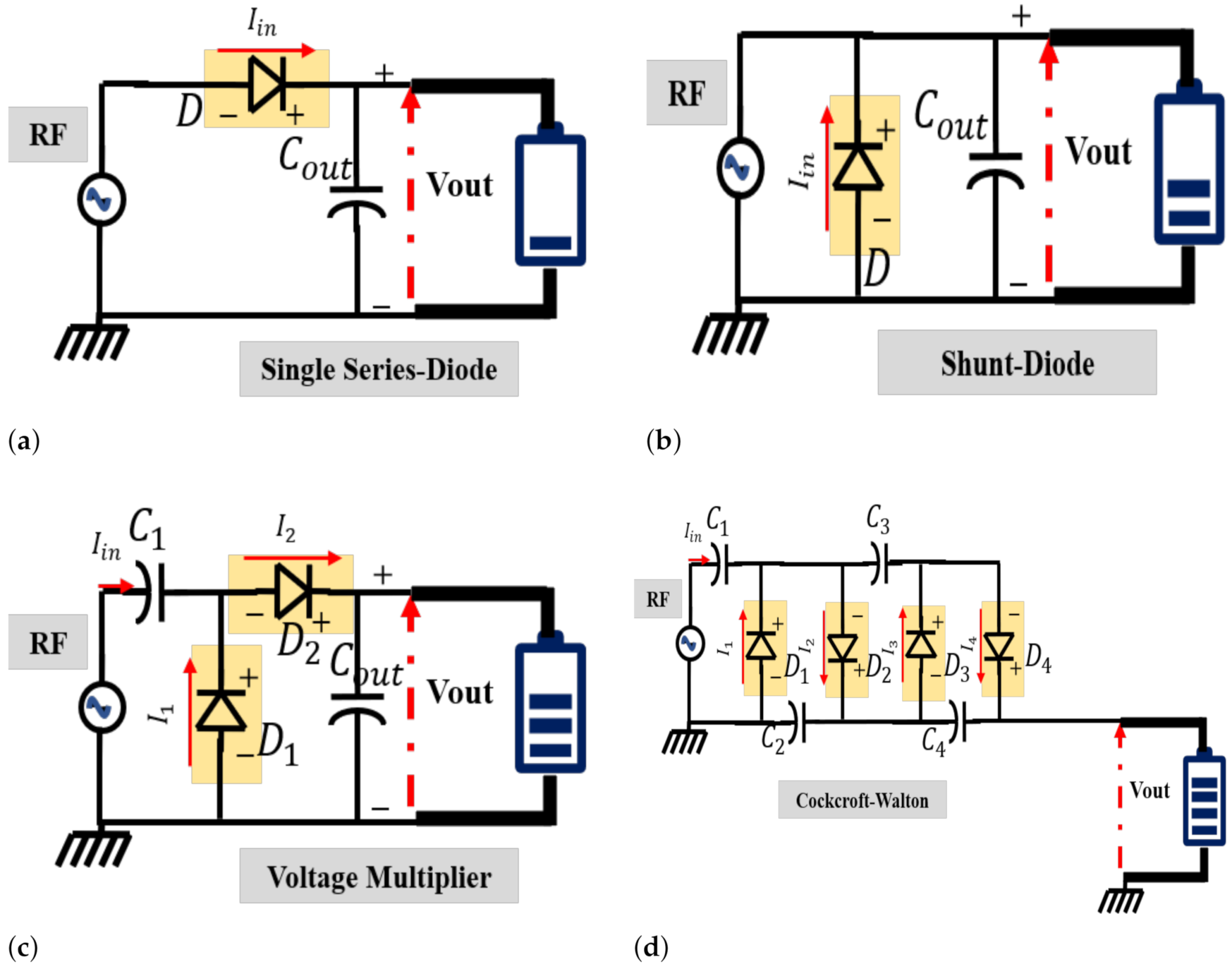
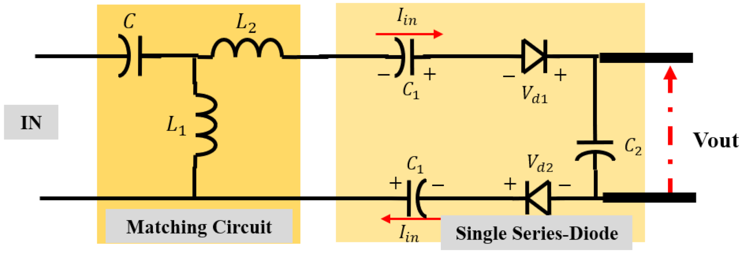
2.1. Single-Series Diode

A single-series diode architecture is chosen as it offers a high efficiency at low power input and it also avoid the losses produced from multiple-diode configuration. It is proven that the balanced single-series diode is the best candidate to provide a balanced output voltage and RF signal noise cancellation at the input port. The schematic circuit is shown in Figure 2. There are two Schottky diodes in the upper and lower branch of the rectifier circuit, the Skyworks SMS7630-061 single diode is chosen due to its low power operation. The current is flowing in the circuit as indicated by the red arrow. The output voltage is taken across the output charging capacitor. The total output voltage is given by:
V o u t = V i n V t
where V i n represents the input RF signal and given by V i n = A c o s t ( ω × t ) and V t indicates the total losses existing in the rectification Schottky Barrier Diodes.
The circuit represents a balance half wave rectifier and its operation is demonstrated as follows: during the positive cycle of the input waveform, the diode D1 is turned on and so is D2. The current in the circuit is flowing as indicated in Figure 2. In contrast, during the negative cycle, neither of the diodes conduct the current; therefore, the output is declined. The output capacitor C2 is used to smooth the output DC voltage and suppress any existing ripples. The balanced operation introduces a great solution to act as a potential alternative power supply for the wireless sensor node-based CMOS technology. The impedance of the rectifier input tends to be capacitive; therefore, it is compensated using an impedance matching network.

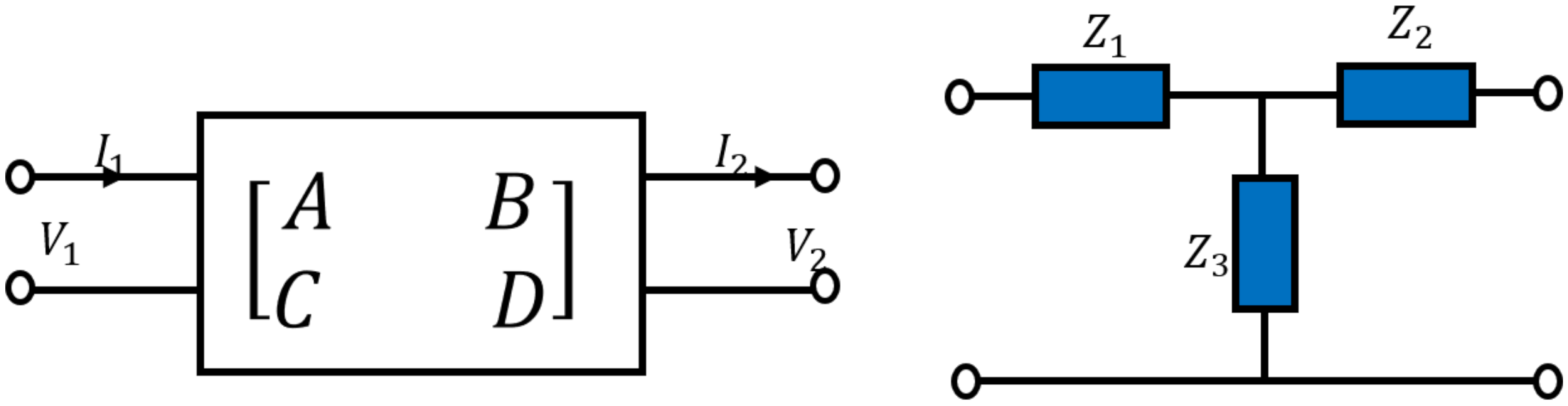
2.2. Impedance Matching Circuit

The rectifier architecture uses a single-series diode topology. A dual-band matching network operating at 900 MHz and 2.45 GHz is inserted prior the rectifier input. It is composed of a T-network in which there is a series arm represented by capacitor C and an inductance denoted by L 2 , and the shunt branch is composed of an inductance L 1 .
The mathematical analysis of the matching circuit is demonstrated in this section. The T-matching circuit can be represented by a two-port ABCD matrix as shown in Figure 3.
1 + Z 1 / Z 3 Z 1 + Z 2 + ( Z 1 Z 3 ) / Z 3 1 / Z 3 1 + Z 2 / Z 3 where Z 1 = 1 j ω C , Z 2 = j ω L 2 , Z 3 = j ω L 1
after long mathematical calculation, we can derive A, B, C and D as
A = 1 1 ω 2 L 1 C B = j ω 2 L 1 L 2 C ( L 1 + L 2 ) ω L 1 C C = 1 j ω L 1 D = 1 + L 2 L 1
The ABCD matrix can be used to predict the total input impedance of the matching circuit. The total input impedance of ABCD matrix is calculated by the following equation:
Z i n = A + B Z o C + D Z o
where Z o represents the input characteristic impedance of the rectifier circuit. The resonance frequencies are given by:
f 1 = 1 2 π L 2 C , f 2 = L 1 + L 2 2 π L 1 L 2 C
As indicated in Equation (5), the two resonance frequency are tuned by the values of L 1 , L 2 and C. In order to get resonance at 0.92 and 2.4, the values of matching components are given as follows: L 1 = 30 nH, L 2 = 6.5 nH and C = 0.8 pF. Those values produce typical resonance frequencies at 0.93 and 2.4 GHz, respectively. The voltage standing wave ratio (VSWR) for the matching circuit and rectifier is shown in Figure 4. The VSWR for the three conditions is demonstrated. In the first case, when the inductance L 2 in the matching circuit is removed. The circuit is completely matched at the 920 MHz and partially matched around 2.4 GHz. However, with removing L 1 , the circuit offers total matching around 2.4 GHz rather than 920 MHz. By employing both inductors, the circuit provide good matching condition at either 920 MHz and 2.4 GHz. This satisfies the desired dual-band frequency operation.

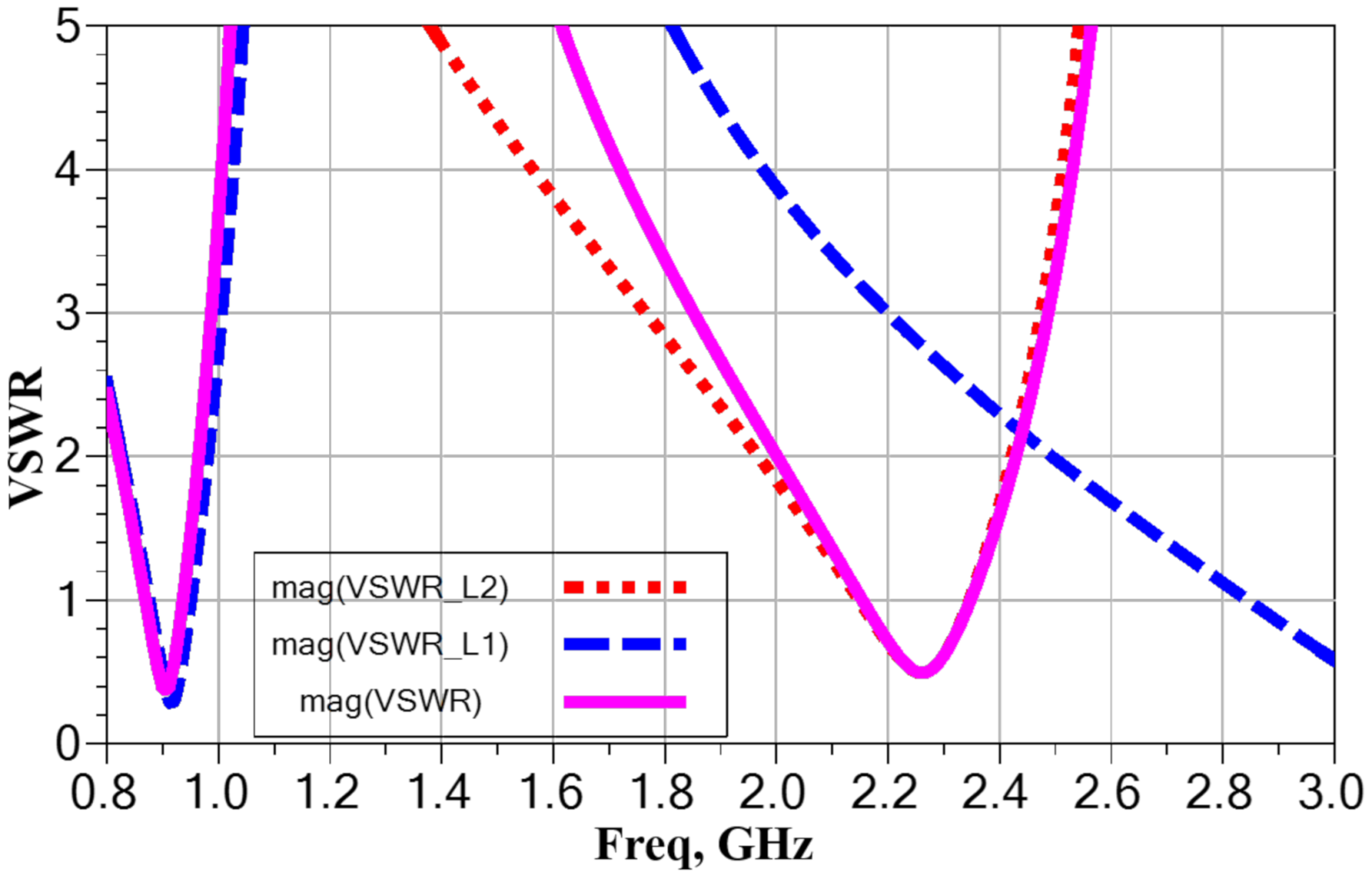
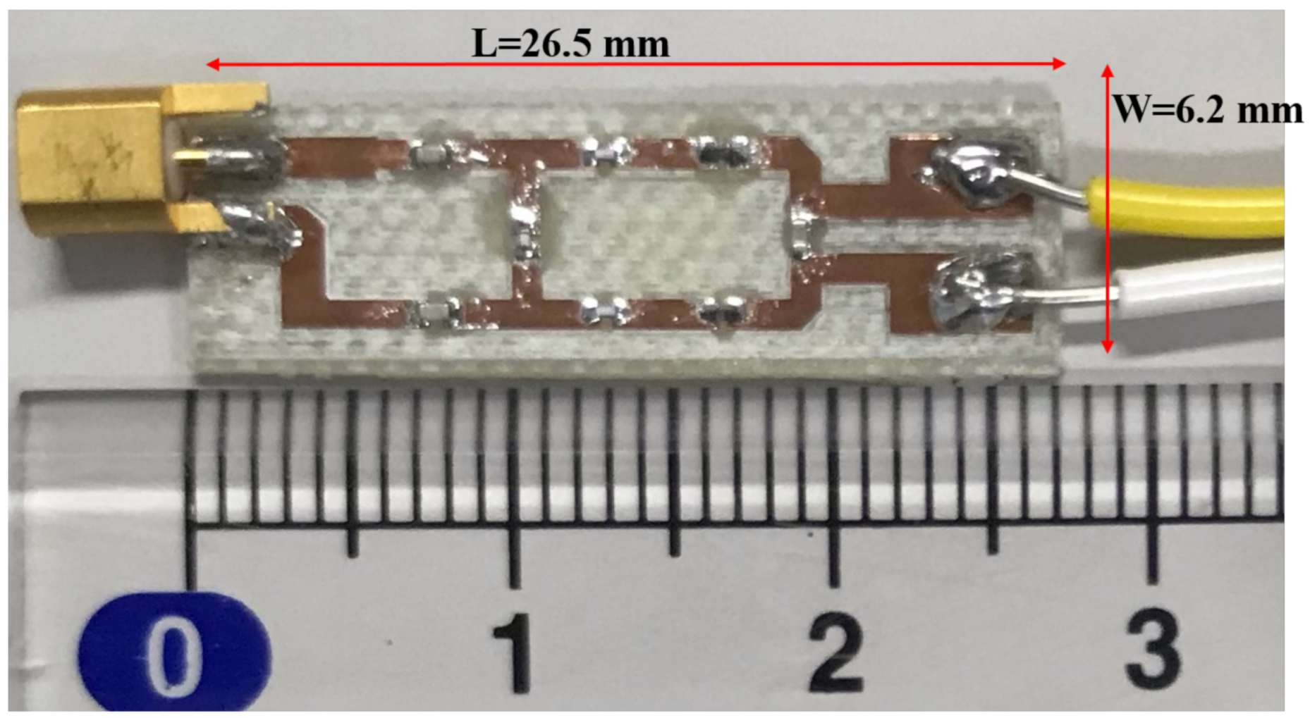
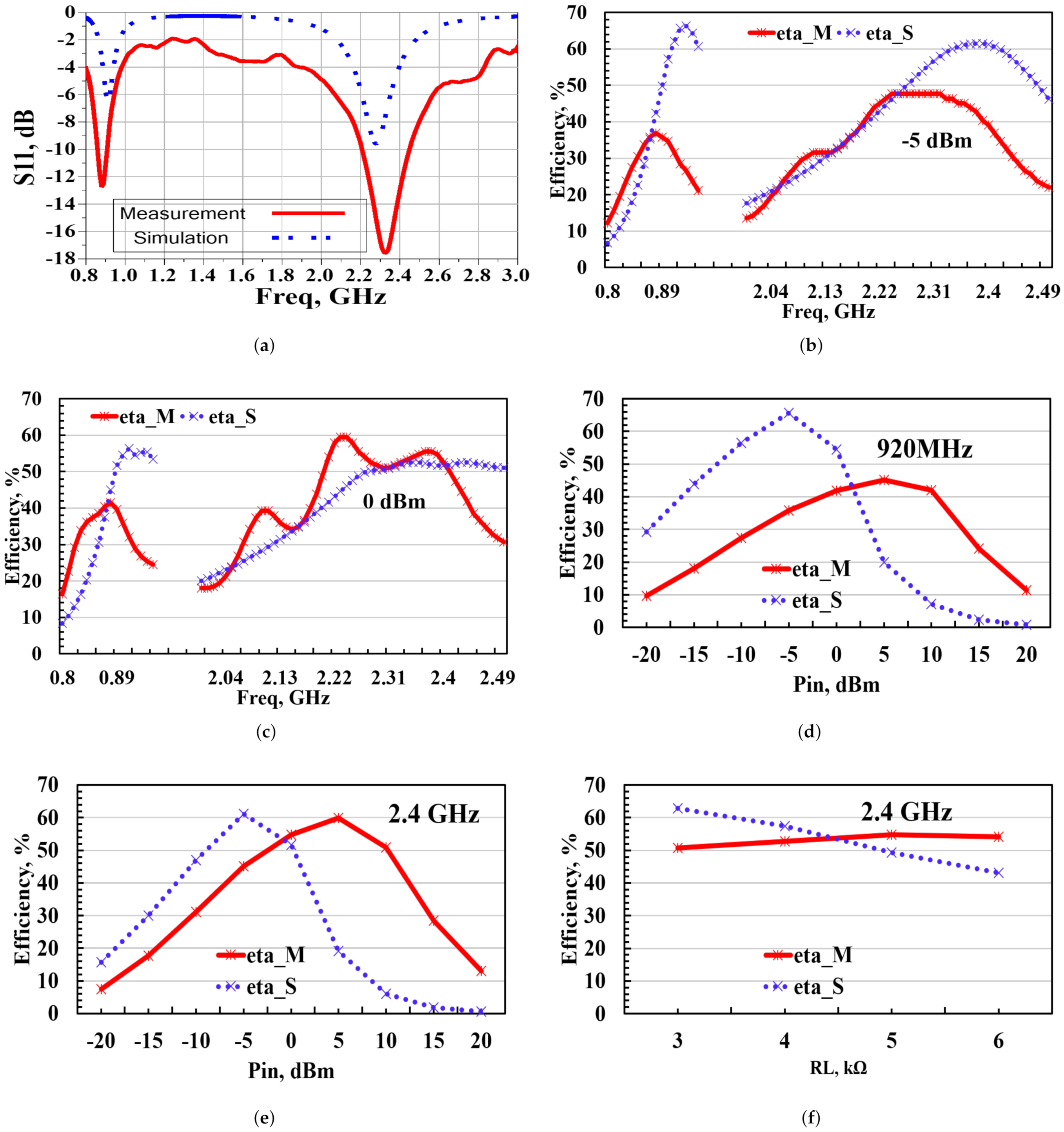
3. Simulation and Experimental Results

In this section, the rectifier characterization and measurement results are discussed. A prototype circuit is fabricated on a single layer commercial FR4 substrate with a dielectric constant ε r = 4.4 and thickness h = 0.8 mm. The fabricated rectifier circuit layout is shown in Figure 5. It is implemented using differential coplanar strip line (CPS) port. The port exhibit 50 Ω input impedance that can be interfaced with the standard coaxial connector.
In order to demonstrate the rectifier performance, the efficiency definition in Equation (6) is used. Several parameters are tuned concurrently to derive the full rectifier characteristics. First, the load resistance and the input power are fixed at 5 k Ω and −5, 0, 5 dBm, respectively. Then, the frequency is changed from 0.8 to 0.95 GHz for the lower band and from 2 to 2.5 GHz at the higher band. The output voltage is evaluated, and the output conversion efficiency is estimated using the following equation:
η = P d c P r f = V d c R L 2 × P r f × 100 %
where P d c is the output DC power, P r f is the RF input power signal, and V d c is the output DC voltage. The comparison between the measurement and simulated results is shown in Figure 6.
The input reflection coefficient is shown in Figure 6a. As can be observed, there are two valleys in the S11 curve. The first is achieved at 920 MHz with a typical −6 dB impedance bandwidth of 80 MHz, whereas the second minimum is given at 2.4 GHz with a wider bandwidth of 300 MHz. There is no power transmission in the region between the two bands and this verifies the dual-band operation at the desired frequency ranges. It is noted that both simulation and measurements are exactly matched at both bands, with measurement results more robust than simulation.
The efficiency versus frequency curves are estimated and shown in Figure 6b,c; the curves were plotted at input power of −5 and 0, respectively. For the −5 dBm case, the simulation and measurements are slightly matched but there is a prominent difference at the lower frequency band. While the simulation results reaches up to 62%, the measurements are decreasing to 35%. This difference can be attributed to the connector losses, diode non-linearity and the fabrication tolerance.
The difference decreases when the power is maximized to 5 dBm. In this case, both lower and higher bands are greatly matched and the numerical data are approaching. When the power is raised to 5 dBm, the measured results outperform the simulation. This happens due to the optimum operating power point of the real rectifier which is shifted to the higher range of input signal strength.
The variation of efficiency with respect to the input power is shown in Figure 6d,e. The lower band performance is illustrated in Figure 6d at 920 MHz. As expected the peak efficient power of the measured results is shifted to the upper range of the input power, there is 8 dBm difference. The higher-band performance at 2.4 GHz is typically matched together with a slight shift in the input power. The peak efficiency reached up to 60% and it was achieved at 5 dBm. The power shift is due to the attenuation ohmic losses in the transmission lines which causes the diode to initialize the conduction at more higher input power values than the expected theoretical region. The metal losses are inevitable and cannot be neglected or eliminated.
The changes in efficiency with respect to the terminal load are explained in Figure 6f for the upper frequency band. The peak efficiency of 60% is achieved at an optimum terminal load of 5 k Ω . It can be seen that the efficiency curves are sensitive to the change of the resistor values.
The slight mismatch is attributed to various circuit losses which were not considered during efficiency estimation. For instance, device parasitics can cause a considerable decrease in the efficiency. The diode junction resistance R s can limit efficiency of the diode as the current flowing through the diode will dissipate power in the semiconductor junction [21].
In order to reflect the benefits of the proposed rectifier, a comparative study is conducted in Table 1. The main aspects included in the table are the technology used, rated output voltage, operating frequency, terminal load resistance, achieved overall conversion efficiency, and the prototype size. Although the design discussed in [18] achieves a prominent advantage in terms of the overall efficiency at either band, the large footprint and high power rating hinder its use for low-power energy harvesting applications. Similarly, all other designs lack either high efficiency operation or large DC voltage supply. The proposed design uses a simple configuration compared to other prototypes introduced in the literature. The other important characteristic of the proposed rectifier is the high efficiency achieved at either frequency band; the peak efficiency reaches up to 60%. Regarding prospective output voltage, the proposed rectifier can deliver a maximum output voltage of 2.66 V to a load of 4.7 k Ω at 5dBm. Such advantages qualify the proposed rectifier as a good candidate for wireless energy transfer for low-power wireless applications.

4. Conclusions

In this study, an efficient dual-band ISM RF energy-harvesting rectifier operating at 900 MHz and 2.45 GHz was optimized, characterized and the maximal performance was achieved. The proposed circuit could efficiently harvest power from a dedicated microwave source that emits a signal with an input power ranging from −15 to 20 dBm. The proposed system achieved a power conversion efficiency of more than 60% over the lower and higher frequency band. The significant merit of the proposed design is the simplicity of circuit-design and single-layer fabrication.

Author Contributions

Conceptualization, M.M.M.; methodology, M.M.M.; software, M.M.M.; validation, M.M.M. and H.K.; formal analysis, M.M.M., S.T. and S.Y.; investigation, M.M.M.; resources, H.K.; data curation, M.M.M.; writing—original draft preparation, M.M.M., S.T. and S.Y.; writing—review and editing, H.K.; visualization, M.M.M.; supervision, H.K.; project administration, H.K.; funding acquisition, H.K. All authors have read and agreed to the published version of the manuscript.

Funding

This work was partially supported by the Cabinet Office (CAO), Cross-ministerial Strategic Innovation Promotion Program (SIP; JPNP18014), “An intelligent knowledge processing infrastructure, integrating physical and virtual domains” (funding agency: NEDO), SCOPE, and KAKENHI (JP18K04146) JSPS.

Acknowledgments

Authors would like to thank VLSI Design and Education Center (VTEC), the University of Tokyo in collaboration with CADENCE Corporation and Keysight Technologies who provided the simulation software and tools for simulations and results verification. Moreover, we would like to thank our colleagues at the Electronic Devices Lab. in Kyushu university for the fruitful discussion and consultations.

Conflicts of Interest

The authors declare no conflict of interest.

References

  1. Thierry, T.; Ludivine, F.; Laurent, O.; Florent, T.; Valérie, V. RF energy harvesting and remote powering at 900 MHz and 2.4 GHz. In Proceedings of the 2014 21st IEEE International Conference on Electronics, Circuits and Systems (ICECS), Marseille, France, 7–10 December 2014; pp. 818–821. [Google Scholar]
  2. Chandrasekaran, K.T.; Agarwal, K.; Karim, M.F. Compact Dual-Band Metamaterial-Based High-Efficiency Rectenna: An Application for Ambient Electromagnetic Energy Harvesting. IEEE Antennas Propag. Mag. 2020, 62, 18–29. [Google Scholar] [CrossRef]
  3. Valenta, C.R.; Durgin, G.D. Harvesting Wireless Power: Survey of Energy-Harvester Conversion Efficiency in Far-Field, Wireless Power Transfer Systems. IEEE Microw. Mag. 2014, 15, 108–120. [Google Scholar]
  4. Wang, X.; Mortazawi, A. Rectifier array with adaptive power distribution for wide dynamic range RF-DC conversion. IEEE Trans. Microw. Theory Techn. 2019, 67, 392–401. [Google Scholar] [CrossRef]
  5. Rotenberg, S.A.; Podilchak, S.K.; Lee, J. Efficient rectifier for wireless power transmission systems. IEEE Trans. Microw. Theory Techn. 2020, 68, 1921–1932. [Google Scholar] [CrossRef]
  6. Kuhn, V.; Lahuec, C.; Seguin, F.; Person, C. A multi-band stacked RF energy harvester with RF-to-DC efficiency up to 84%. IEEE Trans. Microw. Theory Tech. 2015, 63, 1768–1778. [Google Scholar] [CrossRef]
  7. Lu, J.; Yang, X.; Mei, H.; Tan, C. A four-band rectifier with adaptive power for electromagnetic energy harvesting. IEEE Microw. Wireless Compon. Lett. 2016, 26, 819–821. [Google Scholar] [CrossRef]
  8. Mansour, M.; Kanaya, H. Compact and Broadband RF Rectifier with 1.5 Octave Bandwidth Based on a Simple Pair of L-Section Matching Network. IEEE Microw. Wirel. Compon. Lett. 2018, 28, 335–337. [Google Scholar] [CrossRef]
  9. Mansour, M.; Polozec, X.L.; Kanaya, H. Enhanced Broadband RF Differential Rectifier Integrated with Archimedean Spiral Antenna for Wireless Energy Harvesting Applications. Sensors 2019, 19, 655. [Google Scholar] [CrossRef] [PubMed] [Green Version]
  10. Scorcioni, S.; Larcher, L.; Bertacchini, A. A reconfigurable differential CMOS RF energy scavenger with 60% peak efficiency and sensitivity. IEEE Microw. Wireless Compon. Lett. 2013, 23, 155–157. [Google Scholar] [CrossRef]
  11. Niotaki, K.; Georgiadis, A.; Collado, A. Dual-band rectifier based on resistance compression networks. IEEE MTT-S Int. Dig. 2014, 32, 1–3. [Google Scholar]
  12. Kanaya, H.; Tsukamoto, S.; Hirabaru, T.; Kanemoto, D.; Pokharel, R.; Yoshida, K. Energy Harvesting Circuit on a One-Sided Directional Flexible Antenna. IEEE Microw. Wirel. Compon. Lett. 2013, 23, 164–166. [Google Scholar] [CrossRef]
  13. Mansour, M.; Kanaya, H. Compact RF rectifier circuit for ambient energy harvesting. In Proceedings of the IEEE International Symposium on Radio-Frequency Integration Technology (RFIT), Seoul, Korea, 30 August–1 September 2017; pp. 220–222. [Google Scholar]
  14. Mansour, M.; Yamamoto, S.; Kanaya, H. Reconfigurable Multistage RF Rectifier Topology for 900 MHz ISM Energy-Harvesting Applications. IEEE Microw. Wirel. Compon. Lett. 2020, 30, 1181–1184. [Google Scholar] [CrossRef]
  15. Mansour, M.; Kanaya, H. Efficiency—Enhancement of 2.45 GHz Energy Harvesting Circuit Using Integrated CPW—MS Structure at Low RF Input Power. IEICE Trans. Electron. 2019, E102-C, 399–407. [Google Scholar] [CrossRef]
  16. Liu, Z.; Zhong, Z.; Guo, Y. Enhanced Dual-Band Ambient RF Energy Harvesting with Ultra-Wide Power Range. IEEE Microw. Wirel. Compon. Lett. 2015, 25, 630–632. [Google Scholar] [CrossRef]
  17. Li, C.; Yu, M.; Lin, H. A Compact 0.9-/2.6-GHz Dual-Band RF Energy Harvester Using SiP Technique. IEEE Microw. Wirel. Compon. Lett. 2017, 27, 666–668. [Google Scholar] [CrossRef]
  18. Du, Z.; Zhang, X. High-Efficiency Single- and Dual-Band Rectifiers Using a Complex Impedance Compression Network for Wireless Power Transfer. IEEE Trans. Ind. Electron. 2018, 65, 5012–5022. [Google Scholar] [CrossRef]
  19. Mattsson, M.; Kolitsidas, C.; Jonsson, B. Dual-band dual-polarized full-wave rectenna based on differential field sampling. IEEE Antennas Wireless Propag. Lett. 2018, 17, 956–959. [Google Scholar] [CrossRef]
  20. Liu, J.; Huang, M.; Du, Z. Design of Compact Dual-Band RF Rectifiers for Wireless Power Transfer and Energy Harvesting. IEEE Access 2020, 8, 184901–184908. [Google Scholar] [CrossRef]
  21. Yoo, T.; Chang, K. Theoretical and experimental development of 10 and 35 GHz rectennas. IEEE Trans. Microwave Theory Tech. 1992, 40, 1259–1266. [Google Scholar] [CrossRef]
  22. Khemar, A.; Kacha, A.; Takhedmit, H.; Abib, G. Design and experiments of a dual-band rectenna for ambient RF energy harvesting in urban environments. IET Microw. Antennas Propag. 2018, 12, 49–55. [Google Scholar] [CrossRef]
Figure 1. Various RF–DC rectification schemes, (a) Series-diode connection, (b) Shunt-diode connection, (c) Voltage multiplier, (d) Cockcroft–Walton multilevel configuration. It is observed that whenever the voltage level increases, the terminal battery voltage level increases as well.
Electronics 10 01764 g001
Figure 2. The rectifier circuit topology. It composed of a T-matching circuit followed by a single-series balanced diode. The output voltage can feed any resistive load which lies in the optimum resistance load of the rectifier circuit.
Electronics 10 01764 g002
Figure 3. Representation of a two-port ABCD matrix for the T-Matching network.
Electronics 10 01764 g003
Figure 4. Comparison of the simulated VSWR with different circuit condition. VSWR-L1:VSWR with connection of only L1 and removing L2. VSWR-L2: VSWR with connection of only L2 and removing L1. VSWR: VSWR with connection of both L1 and L2.
Electronics 10 01764 g004
Figure 5. Photograph of the fabricated rectifier prototype. The circuit size is comparatively small and can simply be integrated with a high-gain antenna.
Electronics 10 01764 g005
Figure 6. The measured and simulated rectifier performance comparison (a) Return loss, S11 which describe the level of impedance matching of the rectifier circuit, (b) Efficiency variation with the input frequency estimated input power P i n = −5 dBm, and R L = 5 k Ω , (c) Efficiency variation with the input frequency estimated input power P i n = 0 dBm, and R L = 5 k Ω , (d) Efficiency changes with the input power at lower band frequency 920 MHz, and R L = 5 k Ω (e) Efficiency changes with the input power at higher band frequency 2.4 GHz, and R L = 5 k Ω , (f) Efficiency changes with the load terminal at the higher band frequency 2.4 GHz and Pin = 5 dBm. M: stands for measurements and is given in solid red line, and S: stands for simulations and is given in dotted blue line.
Electronics 10 01764 g006
Table 1. Comparison of the current work with some architectures in the literature.
[16][17][22][18][19][20]This Work
TechnologyAvago 2850CMOS 0.18umSMS7630HSMS 286FHSMS2850SMS 7630SMS 7630
V d c V@dBm6.2@201.3@-150.3@-7N/AN/A1@02.66@5
f c GHz0.9, 1.80.9, 2.6GSM1800, UMTS-12.45, 5.82.4, 5.50.915, 2.45ISM 0.92, 2.4
R L k Ω 2.55001.50.36152.54.7
η % @dBm30@-15 to 2037.5@1338@-972@1838@069@-165@0
SizeN/A11.6 mm 2 104 mm 2 1542 mm 2 1750 mm 2 1880 mm 2 156 mm 2
Publisher’s Note: MDPI stays neutral with regard to jurisdictional claims in published maps and institutional affiliations.

