Article

An 18-Gb/s/pin Single-Ended PAM-4 Transmitter for Memory Interfaces with Adaptive Impedance Matching and Output Level Compensation

1
Department of Electrical and Computer Engineering, Seoul National University, Seoul 08826, Korea
2
Inter-University Semiconductor Research Center (ISRC), Seoul National University, Seoul 08826, Korea
3
Department of Electronics and Communications Engineering, Kwangwoon University, Seoul 01897, Korea
*
Author to whom correspondence should be addressed.
Submission received: 24 June 2021 / Revised: 20 July 2021 / Accepted: 21 July 2021 / Published: 24 July 2021
(This article belongs to the Special Issue High-Speed I/O Circuits and Architectures)

Abstract

:
This paper presents a method for preventing output level distortion while matching the channel impedance in the single-ended PAM-4 transmitter for memory interfaces. ZQ codes for all four output signal levels were obtained through ZQ calibration and saved in the ZQ code table. The ZQ code generator then adaptively selected the appropriate codes depending on the data pattern and delivered them to the output driver; this can improve the level separation mismatch ratio (RLM) while matching the channel impedance. To validate the effectiveness of our approach, a prototype chip with an active area of 0.035 mm2 was fabricated in a 65 nm CMOS process. It achieved the energy efficiency of 3.09 pJ/bit/pin at 18 Gb/s/pin, and its RLM was 0.971 while matching the channel impedance.

1. Introduction

The demand for high-bandwidth DRAMs is constantly increasing due to the data-centric trend [1,2,3]. DRAM bandwidth can be increased by raising the number of I/O pins or the clock frequency [4]. However, double data-rate (DDR), low-power double data-rate (LPDDR), and graphic double data-rate (GDDR) memories have a pin count limitation, so a higher clock frequency is required to increase the data-rate per pin. However, since power consumption and frequency-dependent channel loss increases at higher frequencies, it is challenging to increase data transfer speeds using non-return-to-zero (NRZ) signaling. Therefore, four-level pulse amplitude modulation (PAM-4) signaling is one of the most promising methods to address this problem [5].
PAM-4 signaling, which can transmit 2 bits per symbol, is more suitable for higher speeds because its clock frequency is only half of that required for NRZ signaling at the same data rate. However, a PAM-4 signal has only one third of the eye height of an NRZ signal, resulting in a signal-to-noise ratio (SNR) attenuation by 9.5 dB [6,7]. In addition, further SNR degradation may occur due to the non-linearity characteristics of the transmitter output [8]; this causes an imbalance between PAM-4 signal levels. Since the overall performance depends on the smallest eye height of the transmitter, it is important to equalize the voltage difference between signal levels [8] while matching the channel impedance at each signal level.
There have been PAM-4 transmitters that adopt a current- or voltage-mode driver, but PAM-4 transmitters using current-mode drivers [6,9,10] consume a lot of power. Therefore, PAM-4 transmitters using voltage-mode drivers, while improving the PAM-4 signal linearity, have been recently reported [5,11,12,13]. However, in previous designs [5,11,12], the signal level distortion cannot be alleviated while matching the channel impedance, or the output impedance is calibrated based on only one output level; thus, impedance mismatch can occur at other signal levels. A PAM-4 transmitter with a three-point ZQ calibration [13] can match the impedance at +3, +1, and −1 levels considering the VDS variation but cannot match the impedance at −3 level with the channel impedance.
To alleviate the above issues, we present a single-ended voltage-mode PAM-4 transmitter with adaptive impedance matching and output level compensation. First, it finds and stores the ZQ codes for each PAM-4 output signal level while matching the channel impedance through a ZQ calibration. When the output driver transmits data, an adaptive ZQ code generator changes the driver codes in real time according to the output signal level; that is, level-dependent adaptive impedance matching and output level compensation are performed.
This paper is organized as follows: in Section 2, we introduce the design considerations for single-ended voltage-mode PAM-4 transmitter; in Section 3, we describe the proposed PAM-4 transmitter design; in Section 4, the measurement results are presented; and in Section 5, we draw the conclusions.

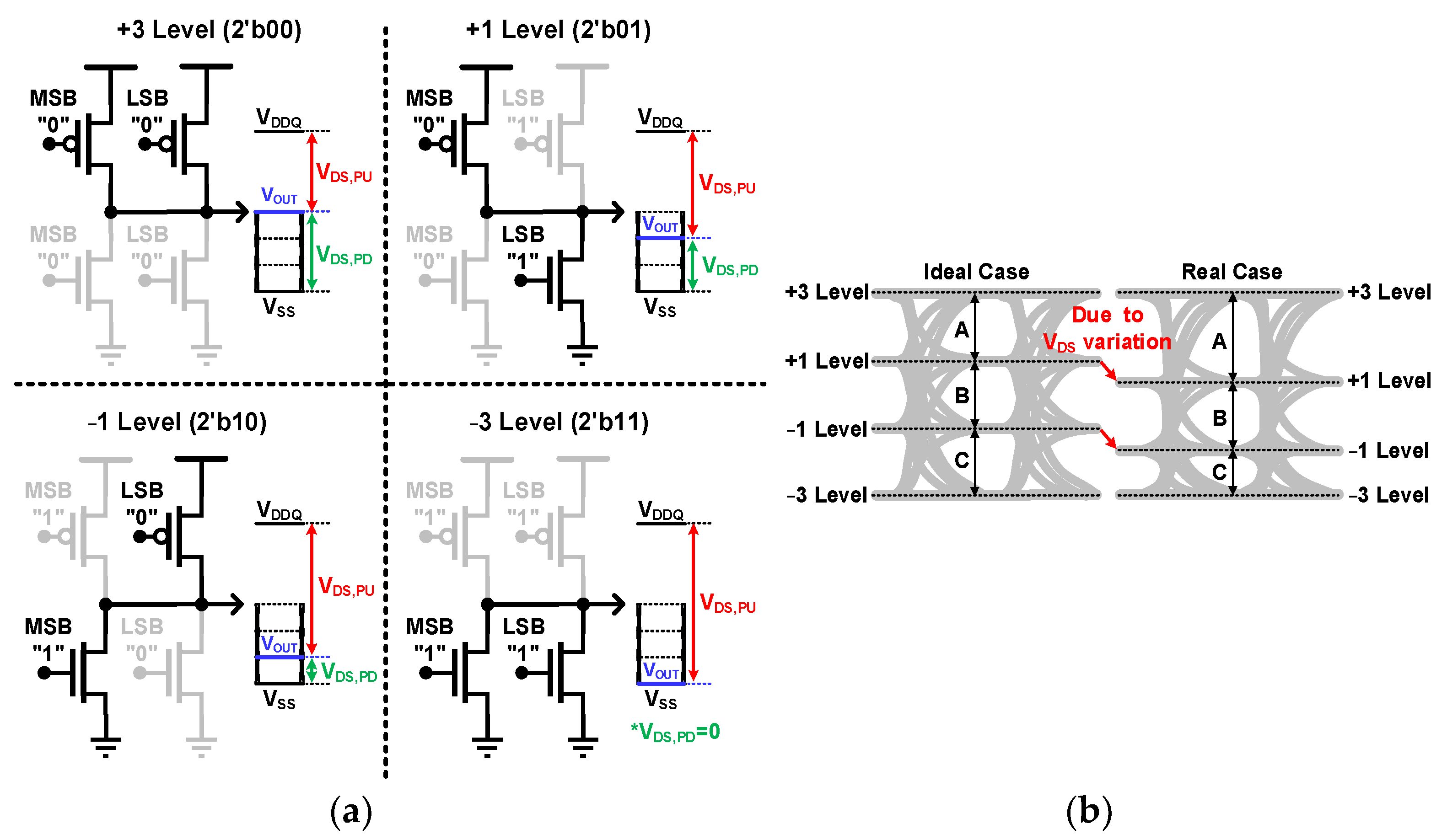
2. Design Considerations

Figure 1a shows VDS variation of the single-ended voltage-mode PAM-4 driver. The variation of VDS,PU and VDS,PD in the pull-up and pull-down transistor occurs as the output signal level changes from one level to another level; this causes variation of the transistor’s on-resistance, distorting the output signal level. Figure 1b shows the output eye diagram considering VDS variation. The output signal level is deviated from the ideal level, deteriorating the level separation mismatch ratio (RLM) that is a function of the intervals between the four PAM-4 output levels. Since the performance of PAM-4 signaling is determined by the smallest eye, calibration for each signal level needs to be made, taking into account VDS fluctuation.
While achieving good RLM performance regarding VDS fluctuation, the channel impedance should be matched because a reflection caused by an impedance mismatch worsens signal integrity. In memory interfaces, impedance matching can be performed through the ZQ calibration. The conventional ZQ calibration is carried out based on one level [5]; thus, the impedance can be mismatched at the other three signal levels that have not been calibrated. The three-point ZQ calibration [13] can match the impedance at +3, +1, and −1 output levels considering VDS variation, improving the linearity. When transmitting the −3 output level, however, the pull-down driver uses the driver codes obtained from the −1 output level. This can cause an impedance mismatch at the −3 output level, leading to the signal reflection. Therefore, it is necessary to match the impedance with the channel for all four signal levels.

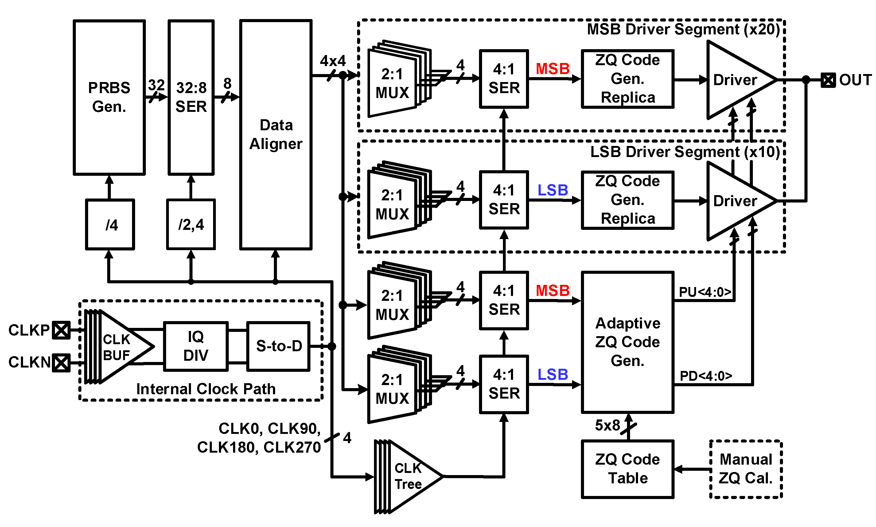
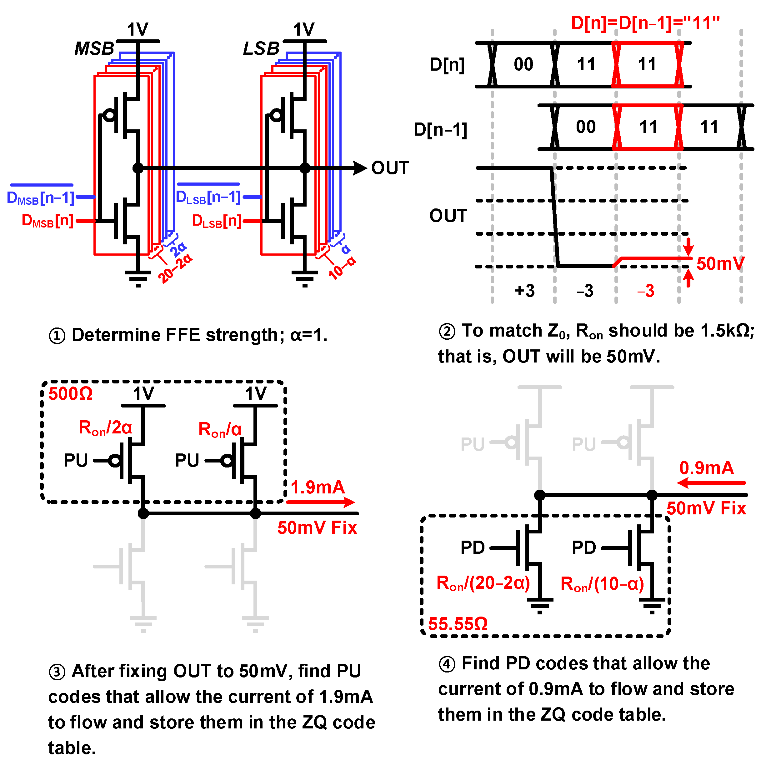
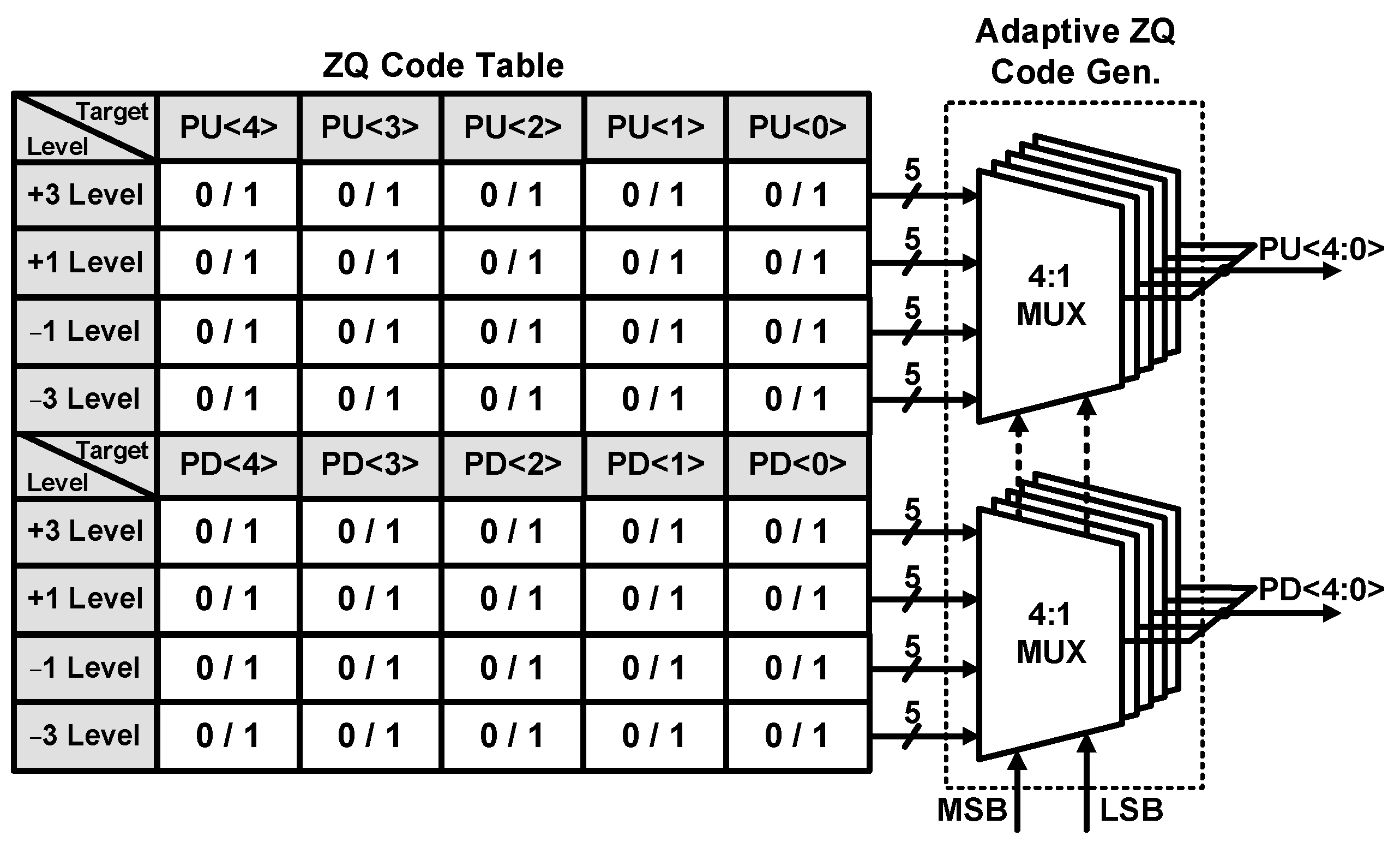
3. Proposed PAM-4 Transmitter

Figure 2 shows a proposed PAM-4 transmitter with four-level impedance matching. The four-phase clock signals (CLK0, CLK90, CLK180, and CLK270) are generated from an internal clock path, which is composed of a clock buffer (CLK BUF), an IQ divider (DIV), and a single-to-differential converter (S-to-D). The 32 bit parallel data generated by a PRBS generator (Gen.) are transmitted to the output driver through a 32:8 serializer (SER), a data aligner, and a 4:1 serializer. The 32:8 serializer is composed of several 2:1 serializers. The most significant bit (MSB) and least significant bit (LSB) drivers are divided into 20 and 10 segments. In each MSB/LSB driver segment, the 2:1 multiplexer (MUX) selects the current or 1-UI delayed data to implement two-tap feed-forward equalization (FFE). The FFE strength is controlled by adjusting the number of segments operating with the current or 1-UI delayed data, and its coefficient can be adjusted up to 13.98 dB. After a ZQ code table is filled by the ZQ calibration, an adaptive ZQ code generator changes the ZQ codes depending on the data pattern and transmits them to the output driver.
To change appropriate ZQ codes in the adaptive ZQ code generator according to the output signal level, the ZQ calibration is first performed for all PAM-4 levels reflecting the FFE strength, and the corresponding ZQ codes are then stored in the ZQ code table. In this prototype, the ZQ calibration is performed manually. Figure 3 shows an example of the manual ZQ calibration using a simplified driver circuit diagram when both current and 1-UI delayed data are “11”. First, we determine the target FFE strength, α, considering channel loss; this example chooses α as 1. Since the on-resistance, Ron, of each transistor should be 1.5 kΩ to match the channel impedance (Z0) of 50 Ω, the output signal level is 50 mV. We then fix OUT to 50 mV in order to find the PU codes at this output level. With the FFE strength of 1, the pull-up resistance should be 500 Ω; thus, the flowing current should be 1.9 mA. After finding the PU codes to achieve this current value, we store these codes in the ZQ code table. Finally, we perform the same process to find the PD codes and store them in the ZQ code table. The ZQ calibration for other PAM-4 signal levels is subsequently followed, obtaining the ZQ codes for all signal levels. Through this process, the ZQ code table is filled. This calibration can be implemented on-chip and performed automatically during the training sequence when applied to the memory system.
The ZQ code table has two 4 × 5 structures for PU/PD codes, as shown in Figure 4. During the ZQ calibration, the ZQ code table is filled with 0 or 1 for all output signal levels. The adaptive ZQ code generator consists of ten 4:1 MUXs. This generator uses the MSB/LSB data to adaptively select codes from the ZQ code table and transmits corresponding codes to the output driver as PU<4:0> and PD<4:0>. The mismatch of the propagation delay between the transmitted codes and the data can degrade the overall performance of our structure. Therefore, a ZQ code generator replica is placed at each driver segment as a delay matching component, as shown in Figure 2.
Figure 5a shows an output driver circuit diagram using a data and driver code encoder [5,13]. When the encoder is placed in front of the output driver, the data and the driver code are encoded, and then encoded data are sent to the output driver; this can make the output driver configuration simple. However, the propagation delay of the data path increases by the delay of the encoder, increasing the power-supply-induced jitter and deteriorating the output drift characteristics in memory interfaces [14]. The proposed output driver in Figure 5b can improve these issues by removing the encoder. Each driver segment has a source-series terminated structure. All segments share a 71 Ω passive resistor to improve linearity, and 5 bit PU/PD codes from the adaptive ZQ code generator control the driver’s on-resistance.
The operation for the conventional [5] and proposed PAM-4 output driver is shown in Figure 6a. In the conventional driver for memory interfaces [5], after ZQ calibration based on the one signal level, PU/PD driver codes are fixed during the burst operation; thus, VDS fluctuation can vary the transistors’ on-resistance, leading to the RLM degradation and the impedance mismatch. Although the previous PAM-4 transmitter with three-point ZQ calibration [13] changes the driver codes according to the data pattern, this structure uses the driver codes obtained from the −1 output level when transmitting the −3 output level; this leads to signal reflection. To alleviate these issues, the PU/PD codes of our driver adaptively change in real time for each output signal level after the ZQ calibration is performed at all four signal levels. Figure 6b shows one example of PD code generation. When the data pattern is changed to ‘11′, ’10′, ‘01′, and ‘00′, the PD<4:0> is changed to ‘01010′, ‘10010′, ‘10011′, and ‘10111′ correspondingly (however, in the conventional structure [5], PD<4:0> is fixed to ‘01010′ regardless of the data pattern). PU<4:0> changes in the same way.

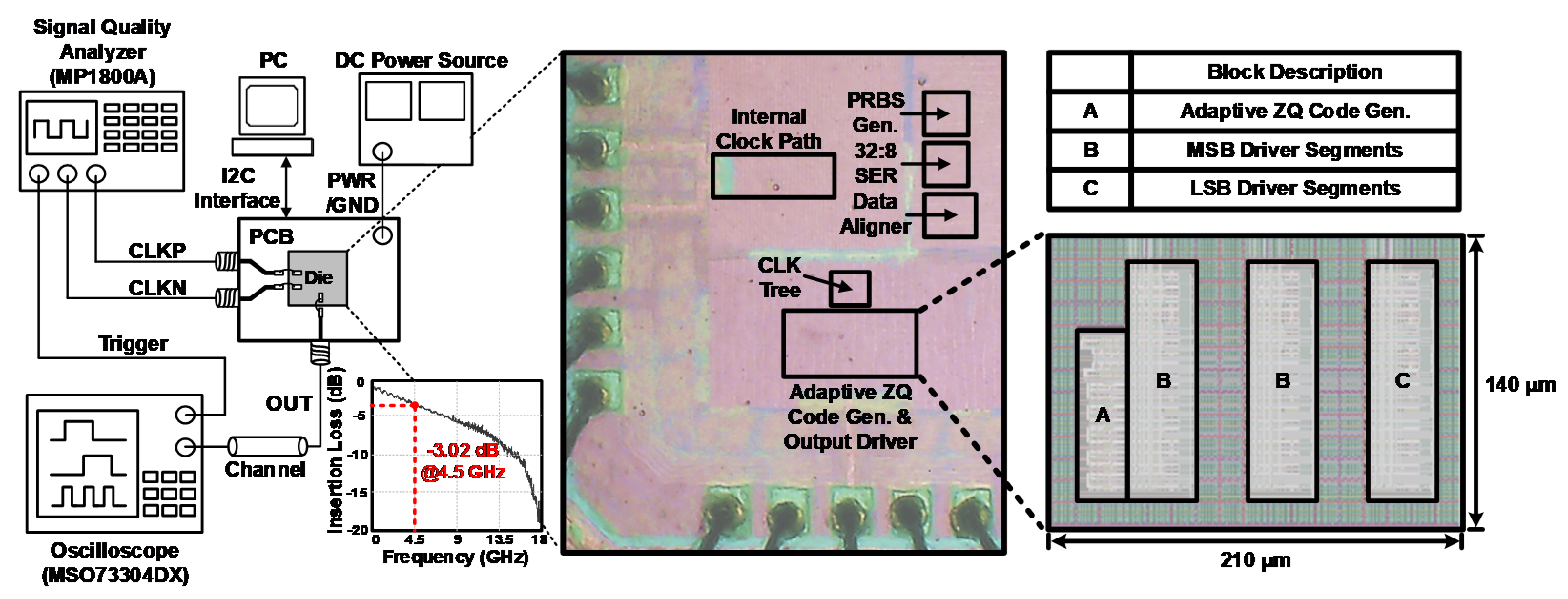
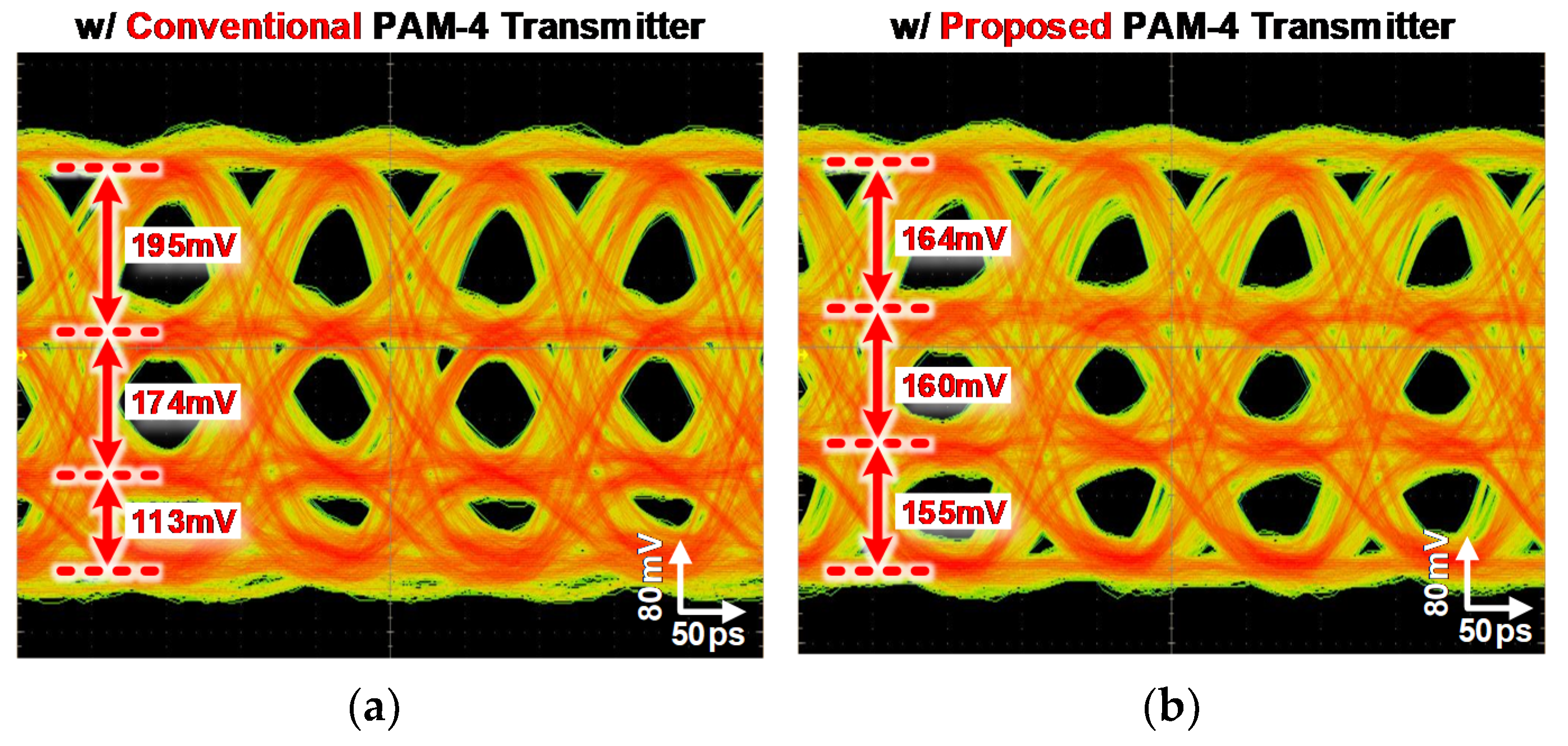
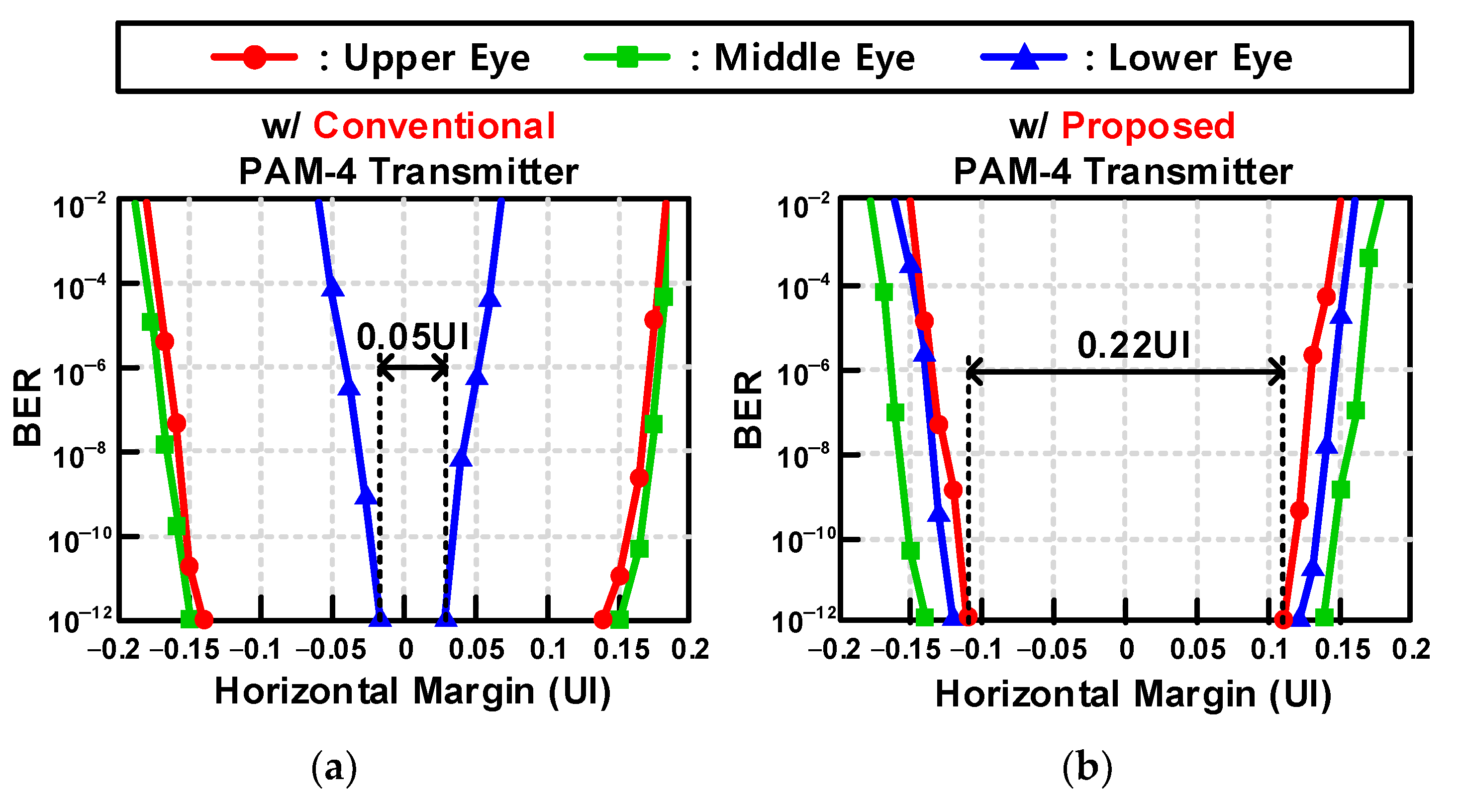
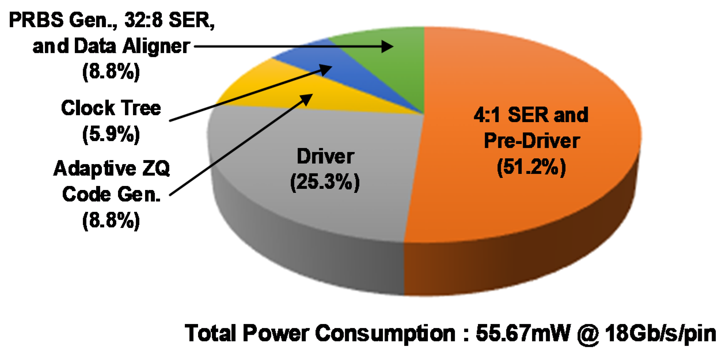
4. Measurement Results

A prototype of the proposed PAM-4 transmitter was fabricated in a 65 nm CMOS process. Figure 7 shows the measurement setup and a die micrograph with a magnified layout. The total active area of the transmitter is 0.035 mm2. The differential clock signals CLKP and CLKN generated by the signal quality analyzer (Anritsu MP1800A) are transmitted to the printed circuit board (PCB), and the output signal passes through a channel where the insertion loss of −3.02 dB at 4.5 GHz is measured on an oscilloscope (Tektronix MSO73304DX). The operation of the transmitter can be controlled externally by means of an inter-integrated circuit (I2C) interface.
Figure 8 shows the measured PAM-4 eye diagrams at 18 Gb/s/pin, with the conventional and proposed PAM-4 transmitter. In this measurement, the PRBS-7 data pattern and the FFE coefficient of 1.94 dB were used. Since the conventional PAM-4 transmitter uses fixed PU/PD codes, eye distortion occurs due to the VDS fluctuation; the voltage gap between signals from top to bottom are 195 mV, 174 mV, and 113 mV, resulting in an RLM of 0.703, and the worst eye height of 32.4 mV (Figure 8a). When the proposed method is applied, eye distortion is compensated; the voltage gap between signals is 164 mV, 160 mV, and 155 mV, respectively, achieving an improved RLM of 0.971 (Figure 8b). With this method, the worst eye-opening also increases to 75.9 mV. Although this method has the better RLM performance, its structure using single-ended signaling may make the PAM-4 eye diagram look somewhat less symmetrical than an eye diagram based on differential signaling [11,12].
Figure 9 shows the measured BER bathtub curves of the upper, middle, and lower eye at 18 Gb/s/pin, with the conventional and proposed PAM-4 transmitter using the PRBS-7 data pattern and the FFE coefficient of 1.94 dB. When the proposed method is not applied, a minimum horizontal margin at a BER of 10−12 is only 0.05 UI (Figure 9a). With the proposed PAM-4 transmitter, the minimum horizontal margin increases to 0.22 UI at a BER of 10−12 (Figure 9b).
Figure 10 shows the power breakdown of the proposed PAM-4 transmitter at 18 Gb/s/pin. The 4:1 SER and pre-driver occupy the largest proportion with 51.2% of the total power consumption, followed by the driver occupying 25.3%.
In Table 1 and Table 2, the performance of our prototype is summarized and compared with those of other recent voltage-mode PAM-4 transmitters. Our transmitter can match the channel impedance at all four PAM-4 signal levels while achieving a good RLM performance by adaptively adjusting the ZQ code according to the data pattern. The ZQ codes are transmitted to the output driver parallel to the data. Thus, the encoder block in front of the output driver can be removed, decreasing the data path delay and improving the output drift characteristic. Although the differential PAM-4 transmitter [8,11] has better energy efficiency, the differential architecture with the on-chip voltage regulator cannot be adopted in memory interfaces. The previous single-ended PAM-4 transmitter [13] has better RLM and energy efficiency performances; however, the impedance values of the NMOS-only driver are vulnerable to the VT variations, and the circuits for the ZQ calibration are needed, even in the main path. Even though the PAM-4 transmitter using the differential ternary R-2R DAC [15] also shows better RLM performance, the impedance calibration is not performed at all signal levels. Furthermore, the bootstrapping method of the R-2R switch is susceptible to the PVT variations, which can vary the output driver’s on-resistance.

5. Conclusions

We have presented an 18 Gb/s/pin single-ended PAM-4 transmitter for memory interfaces with adaptive impedance matching and output level compensation. The driver codes for all PAM-4 signal levels are stored in a ZQ code table after a ZQ calibration. Using an adaptive ZQ code generator, the output driver adjusts the output signal level and impedance for four signal levels to compensate for the VDS variation caused by the output level change. This transmitter achieves an RLM of 0.971 while achieving 3.09 pJ/bit/pin at 18 Gb/s/pin.

Author Contributions

C.H., Y.-U.J. and J.-H.C. proposed the transmitter architecture and wrote the manuscript. C.H. designed and validated the transmitter. S.K. supervised and approved the project and the manuscript. J.-H.C. also supervised the manuscript. All authors have read and agreed to the published version of the manuscript.

Funding

This research received no external funding.

Acknowledgments

This work was supported in part by the Research Resettlement Fund for the New Faculty of Kwangwoon University in 2021.

Conflicts of Interest

The authors declare no conflict of interest.

References

  1. Ko, H.; Kim, M.; Park, H.; Lee, S.; Kim, J.; Kim, S.; Chae, J.H. A controller PHY for managed DRAM solution with damping-resistor-aided pulse-based feed-forward equalizer. IEEE J. Solid-State Circuits 2021. [Google Scholar] [CrossRef]
  2. Bae, W. Supply-scalable high-speed I/O interfaces. Electronics 2020, 9, 1315. [Google Scholar] [CrossRef]
  3. Hollis, T.M.; Stave, E.; Ovard, D.; Greeff, R.; Spirkl, W.; Brox, M.; Taylor, J.; Butterfield, J. Recent evolution in the DRAM interface: Mile-markers along memory lane. IEEE Solid-State Circuits Mag. 2019, 11, 14–30. [Google Scholar] [CrossRef]
  4. Hollis, T.; Brox, M.; Spirkl, W.; Hein, T.; Ovard, D.; Greeff, R.; Lin, D.; Richter, M.; Mayer, P.; Moden, W.; et al. Achieving 16 Gb/s single-ended signaling in high-performance graphics memory. In Proceedings of the 2018 IEEE Workshop on Microelectronics and Electron Devices (WMED), San Francisco, CA, USA, 5–9 February 2018; pp. 1–5. [Google Scholar]
  5. Hollis, T.M.; Schneider, R.; Brox, M.; Hein, T.; Spirkl, W.; Bach, M.; Balakrishnan, M.; Dietrich, S.; Funfrock, F.; Ivanov, M.; et al. An 8Gb GDDR6X DRAM achieving 22Gb/s/pin with single-ended PAM-4 signaling. In Proceedings of the 2021 IEEE International Solid-State Circuits Conference (ISSCC), San Francisco, CA, USA, 20–24 February 2021; pp. 348–349. [Google Scholar]
  6. Zheng, X.; Zhang, C.; Lv, F.; Zhao, F.; Yue, S.; Wang, Z.; Li, F.; Jiang, H.; Wang, Z. A 4–40Gb/s PAM4 transmitter with output linearity optimization in 65nm CMOS. In Proceedings of the 2017 IEEE Custom Integrated Circuits Conference (CICC), Austin, TX, USA, 30 April–3 May 2017; pp. 1–4. [Google Scholar]
  7. Dikhaminjia, N.; He, J.; Hernandez, E.; Tsiklauri, M.; Drewniak, J.; Chada, A.; Zvonkin, M.; Mutnury, B. High-speed serial link challenges using multi-level signaling. In Proceedings of the 2015 IEEE 24th Electrical Performance of Electronic Packaging and Systems (EPEPS), San Jose, CA, USA, 25–28 October 2015; pp. 57–60. [Google Scholar]
  8. Upadhyaya, P.; Poon, C.F.; Lim, S.W.; Cho, J.; Roldan, A.; Zhang, W.; Namkoong, J.; Pham, T.; Xu, B.; Lin, W.; et al. A fully adaptive 19–58 Gb/s PAM-4 and 9.5–29 Gb/s NRZ wireline transceiver with configurable ADC in 16-nm FinFET. IEEE J. Solid-State Circuits 2019, 54, 18–28. [Google Scholar] [CrossRef]
  9. Nazemi, A.; Hu, K.; Catli, B.; Cui, D.; Singh, U.; He, T.; Huang, Z.; Zhang, B.; Momtaz, A.; Cao, J. A 36Gb/s PAM4 transmitter using an 8b 18GS/S DAC in 28nm CMOS. In Proceedings of the 2015 IEEE International Solid-State Circuits Conference (ISSCC), San Francisco, CA, USA, 22–26 February 2015; pp. 58–59. [Google Scholar]
  10. Bassi, M.; Radice, F.; Bruccoleri, M.; Erba, S.; Mazzanti, A. A High-swing 45 Gb/s hybrid voltage and current-mode PAM-4 transmitter in 28 nm CMOS FDSOI. IEEE J. Solid-State Circuits 2016, 51, 2702–2715. [Google Scholar] [CrossRef]
  11. Yang, H.; Roshan-Zamir, A.; Song, Y.; Palermo, S. A low-power dual-mode 20-Gb/s NRZ and 28-Gb/s PAM-4 voltage-mode transmitter. In Proceedings of the 2017 IEEE Asian Solid-State Circuits Conference (ASSCC), Seoul, Korea, 6–8 November 2017; pp. 261–264. [Google Scholar]
  12. Roshan-Zamir, A.; Elhadidy, O.; Yang, H.W.; Palermo, S. A reconfigurable 16/32 Gb/s dual-mode NRZ/PAM4 SerDes in 65nm CMOS. IEEE J. Solid-State Circuits 2017, 52, 2430–2447. [Google Scholar] [CrossRef]
  13. Jeong, Y.-U.; Park, H.; Hyun, C.; Chae, J.-H.; Jeong, S.-H.; Kim, S. A 0.64-pJ/bit 28-Gb/s/pin high-linearity single-ended PAM-4 transmitter with an impedance-matched driver and three-point ZQ calibration for memory interface. IEEE J. Solid-State Circuits. 2021, 43, 2120–2133. [Google Scholar] [CrossRef]
  14. Kim, K.; Chae, J.H.; Yang, J.; Kang, J.; Lee, G.; Byeon, S.; Kim, Y.; Kim, B.; Kim, D.H.; Cho, Y.; et al. A 24Gb/s/pin 8Gb GDDR6 with a half-rate daisy-chain-based clocking architecture and IO circuitry for low-noise operation. In Proceedings of the 2021 IEEE Int. Solid-State Circuits Conference (ISSCC), San Francisco, CA, USA, 14–18 February 2021; pp. 344–346. [Google Scholar]
  15. Lim, B.; Kim, D.; Yoo, C. Voltage-mode PAM4 driver with differential ternary R-2R DAC architecture. Electron. Lett. 2020, 56, 431–432. [Google Scholar] [CrossRef]
Figure 1. (a) VDS variation of a single-ended voltage-mode PAM-4 driver, and (b) output eye diagram of this driver considering VDS variation.
Electronics 10 01768 g001
Figure 2. Overall architecture of a proposed PAM-4 transmitter.
Electronics 10 01768 g002
Figure 3. An example of the manual ZQ calibration using a simplified driver circuit diagram when both current and 1-UI delayed data are “11”.
Electronics 10 01768 g003
Figure 4. The ZQ code table and the adaptive ZQ code generator.
Electronics 10 01768 g004
Figure 5. (a) Output driver using a data and driver code encoder [5,13] and (b) the proposed output driver.
Electronics 10 01768 g005
Figure 6. (a) Operation for conventional [5] and proposed PAM-4 driver and (b) one example of the adaptive PD code generation in the proposed PAM-4 transmitter.
Electronics 10 01768 g006
Figure 7. Measurement setup and die micrograph with the magnified layout.
Electronics 10 01768 g007
Figure 8. Measured PAM-4 eye diagrams (a) with the conventional and (b) proposed PAM-4 transmitter, at 18 Gb/s/pin.
Electronics 10 01768 g008
Figure 9. Measured BER bathtub curves of PAM-4 operation (a) with the conventional and (b) proposed PAM-4 transmitter, at 18 Gb/s/pin.
Electronics 10 01768 g009
Figure 10. Power breakdown of the PAM-4 transmitter at 18 Gb/s/pin.
Electronics 10 01768 g010
Table 1. Transmitter performance summary.
Process65 nm CMOS
Data Rate18 Gb/s/pin
Supply1.0 V/1.2 V
ModulationPAM-4
SignalingSingle-Ended
Driver TypeVoltage-Mode w/Shared R
Equalization2-Tap FFE (De-Emphasis)
Channel Loss @Nyquist−3.02 dB
BER<10−12 (PRBS-7)
RLM0.975 (Simulated)
0.971 (Measured)
Energy Efficiency3.05 pJ/bit/pin (Simulated)
3.09 pJ/bit/pin (Measured)
Area0.035 mm2
Table 2. Comparison with other recent voltage-mode PAM-4 transmitters.
-[5] ISSCC’21[8] JSSC’19[11] ASSCC’17[12] JSSC’17[13] JSSC’21[15] EL’20This Work
Process1 ynm
DRAM
16 nm
FinFET
65 nm
CMOS
65 nm
CMOS
65 nm
CMOS
65 nm
CMOS
65 nm
CMOS
Data Rate
(Gb/s/pin)
2229141628518
Supply (V)1.350.85/0.9/1.2/1/81.0/0.91/0.51.21.0/0.61.01.0/1.2
SignalingSingle-EndedDifferentialDifferentialDifferentialSingle-EndedDifferentialSingle-Ended
Level
Compensation
ZQ Cal.
(Fixed Code)
Impedance
Control Loop
Impedance
Control Loop
LUT 1 + PseudoAnalog Control LoopThree-PointZQ Cal.Impedance
Control Loop
Adaptive ZQ Code Gen.
Impedance Matching
at Four Levels
NoNoNoNoNoNoYes
RLMN/A>0.980.9470.9670.9930.9940.971
pJ/bit/pinN/A1.461.829.90.641.973.09
Area (mm2)54.7 2N/A0.060.060.03330.0730.035
1 Lookup table. 2 Chip area.
Publisher’s Note: MDPI stays neutral with regard to jurisdictional claims in published maps and institutional affiliations.

