1. Introduction
The architecture of the zero-IF (intermediate frequency) transceiver for wireless local area network (WLAN) application has attracted wide interest in recent years, which requires a clean and stable local oscillator (LO) signal [
1]. Generally, LO signals are produced by quadrature LO-generators, and several important circuits of quadrature LO have been developed to achieve low phase noise and high spur suppression. These circuits include the passive RC-CR polyphase filter (PPF) [
2,
3], the quadrature voltage-controlled oscillator (QVCO) [
4,
5], the quadrature divide-by-two divider, and the injection-locked ring oscillator (ILRO) [
6,
7]. PPF generates quadrature signals at the broadband frequency range by cascading multiple stages. However, power consumption is increased because resistive components are also added for cascading more stages. QVCO can achieve low phase noise and wide tuning range, while naturally two LC cores would add chip area and power consumption. Quadrature divide-by-two divider uses a fundamental circuit with a compact area, which has widely been used to generate quadrature LO signals. However, the quadrature divider requires that the former VCO operates at a twice higher frequency, which results in higher consumption. Nevertheless, combinations of multiple methods of quadrature signals are common in recent literature.
Recently, fractional-N frequency planning has experienced rapid development and has attracted more attention [
4,
8,
9,
10,
11,
12], since it can avoid the frequency pulling between power amplifier (PA) and voltage-controlled oscillator (VCO), as well as alleviate the self-mixing and DC offset issues. In [
4,
9,
13], fractional-N frequency planning was mainly achieved by three architectures: combining mixers with multipliers, combining mixers with dividers, and synthesizing digital fractional-N frequency signals. The combination of mixers and dividers has been widely used in WLAN transceivers since it has a simple and comprehensive circuit design. However, the drawback of the method is the high spur level. To reduce the spur level, a single-sideband (SSB) mixer is adopted to generate fractional-N frequency signals, but the capacity of spur suppression is still poor due to harmonic mixing, imbalance, leakage, and some other non-idealities. In addition, the SSB mixer outputs are easily worse when high-speed signals are needed to deliver over the long wires. Thus, one of the challenges of LO delivery is generating clean and stable LO signals with low spur levels when driving long wires of the multi-mm length [
14,
15].
Recent WLAN transceivers have evolved from single-core to multi-cores; thus, LO signals are desired to deliver over longer wires of the multi-mm length, which is the larger load for the input stage. Generally, the LO delivery circuit uses inductive peaking (IP) [
16,
17,
18] circuit to drive long wires of the multi-mm length. A conventional method of combining with inverter-based and IP circuits was reported in [
17], which achieved wideband delivery and good capacity of driving long wires. However, the power consumption is significantly large when it needs to deliver a large swing voltage signal over a long wire. Ref. [
19] used a combination of shunting IP and current-mode-logic (CML) circuits to achieve broadband clock delivery and suppress spur due to driving a capacitive load, while the bandwidth is limited as the single-ended topology and large substrate parasitic capacitance of long wires. The architecture of a combination of splitting wires and shunt IP was proposed in [
20], which can deliver high-speed signals at the wideband frequency, but it suffers from poor power efficiency. An active negative gm-boosting circuit was added to the clock delivery to adjust the gain over a wide frequency range [
21].
To solve the above issues, we compared four types of LO delivery methods using IP circuit; a comparison table is presented to conclude the performance of four LO delivery. Comprehensively, the proposed method of combining the CML-IP circuit with the splitting-wires technique achieves the optimum performance. The major contributions of this paper are listed below:
A fractional-N frequency architecture for WLAN application is presented, and it is reconfigured to select either VCO mode or bypass mode.
Four circuits of LO delivery using the IP circuit to suppress spurs from the SSB mixer are compared.
The proposed LO delivery using CML-IP circuit exhibits comprehensive performance with the low spur, low jitter, and high FoM.
This article focuses on the following: the demand for a high data rate of WLAN transceiver motivates the development of a local oscillator (LO) signal of high quality and integrity. The LO signals for high daterate WLAN applications are desired to not only have proper shape waveforms and adequate voltage amplitude but also to achieve relatively stable and clean outputs with low phase noise and low spur. A fractional-N frequency planning is critical for quadrature LO-generator, which consists of a single-sideband (SSB) mixer and multiple dividers since it can avoid the frequency pulling and alleviate the self-mixing and DC offset issues, while spur levels are easily increased due to harmonic mixing, imbalance, and leakage of the SSB mixer. This article proposes a simple and innovative quadrature LO-generator, which adopts a current-mode-logic (CML) inductive peaking (IP) circuit to improve phase noise and suppress spurious tones.
The remainder of this paper is structured as follows:
Section 2 presents the architecture of the proposed quadrature LO-generator.
Section 3 describes the main circuit blocks, such as the SSB mixer, quadrature divider, clock receiver for bypass mode, and LO delivery. Four LO delivery circuits using the IP technique are also proposed and the performance comparison is discussed in
Section 3.
Section 4 demonstrates the simulated and post-layout simulation results. Finally,
Section 5 concludes the article.
2. The Architecture of the Proposed Quadrature LO-Generator
Figure 1 depicts a block diagram of the proposed quadrature LO-generator.
The frequency planning and design optimization of the LO signals are highly relative to the adopted topology and demands of WLAN transceiver, such as SNR and EVM. The system can be reconfigured to select either VCO mode or bypass mode to support the external VCO as the inputs. Then, it would generate four-phased quadrature LO outputs for the TX mixer and RX mixer, respectively. The LO-generator is designed for a direct conversion transceiver and applied for a 2.4 GHz WLAN band.
The frequency range of the internal VCO is from 6.4 to 6.624 GHz, which can avoid LO pulling by setting the VCO oscillating frequency apart from the transceiver operating frequency. To decrease the spurious tones, a single-sideband (SSB) mixer is used with quadrature inputs produced by two successive quadrature divide-by-two CML dividers. The SSB mixer separately combines the quadrature outputs of two successive dividers to generate differential signals over the frequency range from 4.8 to 4.968 GHz. Then, the LO-frequency plan also consists of a quadrature divide-by-two divider with a 25% duty cycle, with LO signals operating at a frequency from 2.4 to 2.484 GHz.
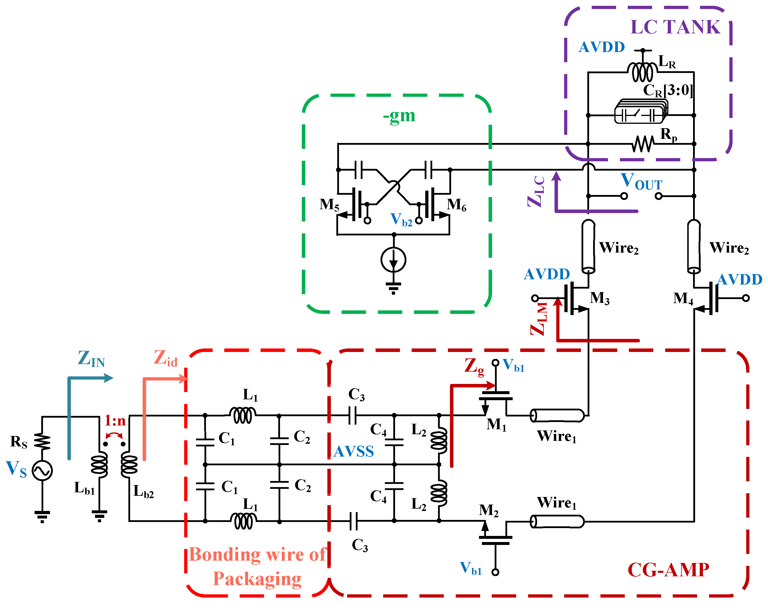
To meet the requirements of a compact and symmetrical floor plan, the clock generated by internal VCO requires driving long wires. The clock needs to deliver over long wires with multi-mm lengths from local VCO to TX and RX mixers, and to suppress spurious tones due to the third-order and fifth-order harmonics mixing, amplitude/phase imbalance, and leakage signals from the inputs to outputs of the SSB mixer. A CML inductive peaking (IP) technique is adopted, and a gm driver of open-drain converts voltage-mode signals to current-mode signals. Then, it uses a three-taped LC tank as the load, which is followed by a cascode transistor. It is desirable to meet the requirement of input voltage swing of the local quadrature divider, and a negative gm (-gm) boosting is adopted to adjust output voltage amplitude.
An external 4.8 GHz VCO for bypass mode can be switched on to independently measure the performance of the LO-generator. Through a common-gate-based clock receiver, the differential output signals of the external VCO are delivered to LC tank, -gm boosting, and quadrature divide-by-two. As shown in
Figure 1, a distributing cascode amplifier is designed to deliver CML signals over the long wires, wires1 and wires2. Then, the CML signals are converted to voltage mode signals by the following LC tank and -gm boosting, providing the inputs of the following quadrature dividers to generate LO signals from 2.4 to 2.484 GHz.
3. Design and Analysis of Proposed Quadrature LO-Generator
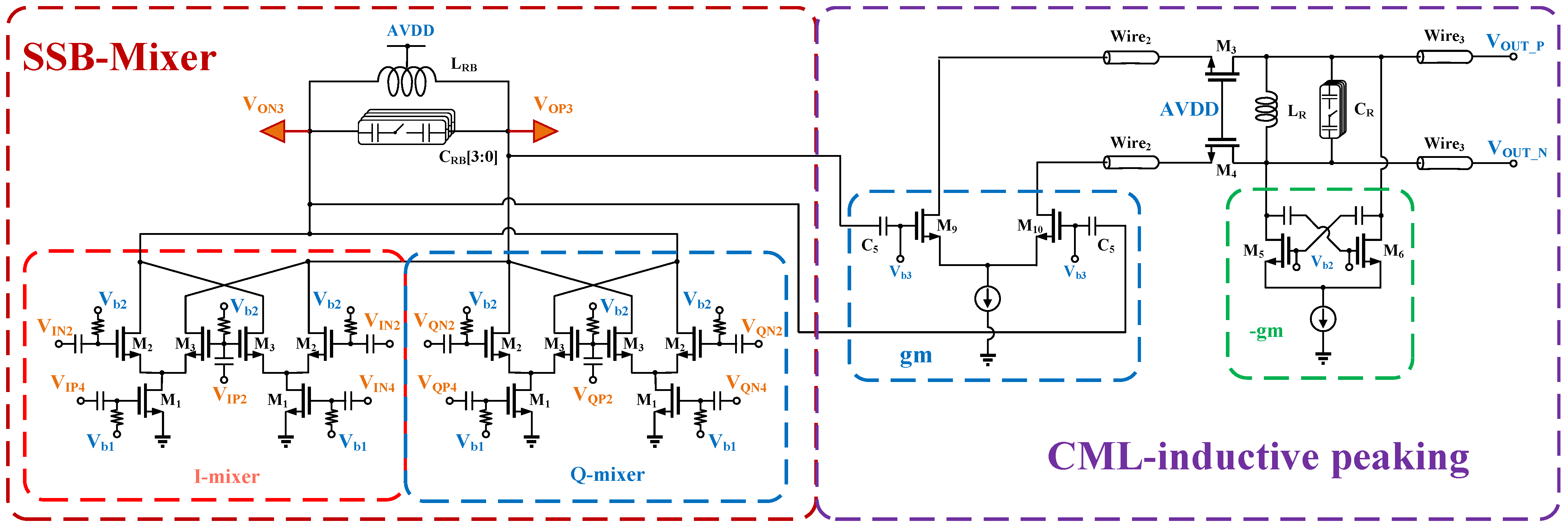
3.1. Single-Sideband (SSB) Mixer
As shown in
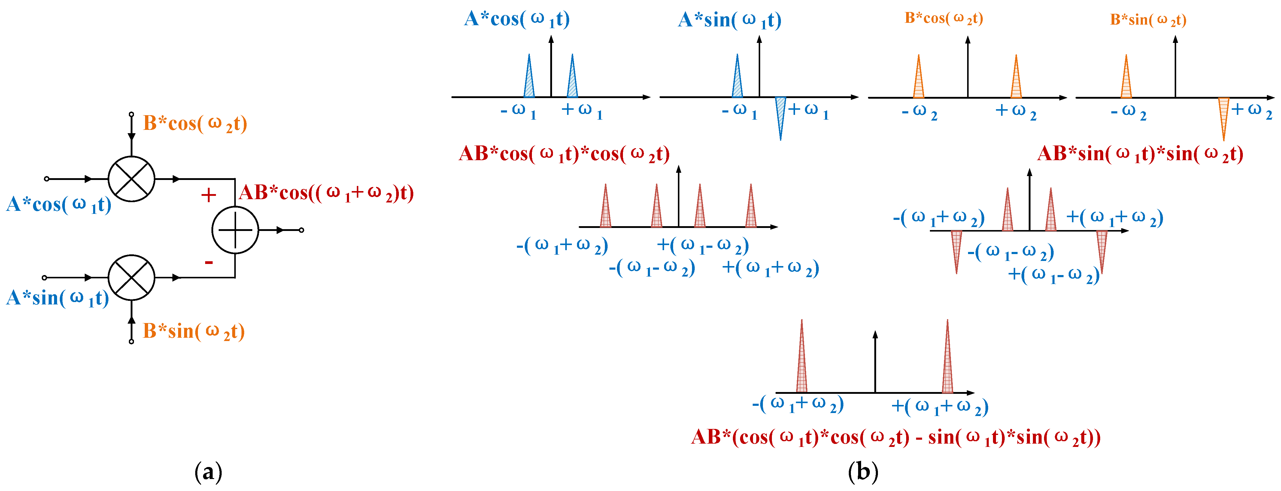
Figure 2a, an SSB mixer is comprised of two mixer cores, which are an in-phase (I) mixer and a quadrature-phase (Q) mixer. It can be selected as either an I/Q up-converter or an I/Q down-converter.
Figure 2b illustrates that the undesired lower sideband is naturally suppressed when it is used for the SSB up-converter. As shown in
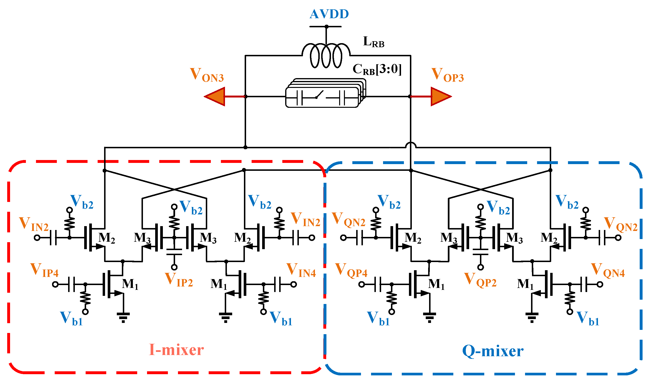
Figure 3, the SSB mixer requires two Gilbert-based cells, I-Gilbert and Q-Gilbert, sharing a common LC tank load. Compared with QVCO, it can save significant chip area and power consumption. The quadrature input signals are produced by two successive CML dividers, and the frequencies of input signals are 3.2 GHz and 1.6 GHz, respectively.
This fractional frequency planning takes an advantage of avoiding frequency pulling and pushing between PA and VCO, and it can alleviate the self-mixing and DC offset issues [
22,
23,
24].
Based on the block diagram of an SSB up-converter, the output products can be derived as follows:
In many WLAN applications, low spur LO outputs are demanded. As shown in
Figure 2a,b, which assumes
, the production output of the SSB mixer is only a single tone, while the input is considered as an ideal single tone, and it is assumed that input signals have equal amplitudes and precise quadrature phases. However, input signals consist of odd harmonics of the fundamental frequency, which causes harmonic mixing, especially the third- and fifth-order harmonics. Phase/amplitude imbalance also exists between quadrature input signals due to design and fabrication mismatch. Thus, the output spectrum of the SSB mixer would present undesirable frequency components due to harmonic mixing, imbalance, leakage signals, and some other non-idealities. Even though the LC tank can suppress undesirable spurious tones, it is still limited due to the tradeoff between the bandwidth and capacity of the sideband suppression. Furthermore, it is a challenge to deliver high-speed signals over a long wire of the multi-mm length and obtain high spur suppression at the end of the long wire. Considering the interferer conditions and the wanted signal-to-noise ratio (SNR) [
1], it is demanded below −45 dBc spurious suppression at the 2.4 GHz frequency band to avoid the harmful out-of-band interferers down-converting to the required sub-bands.
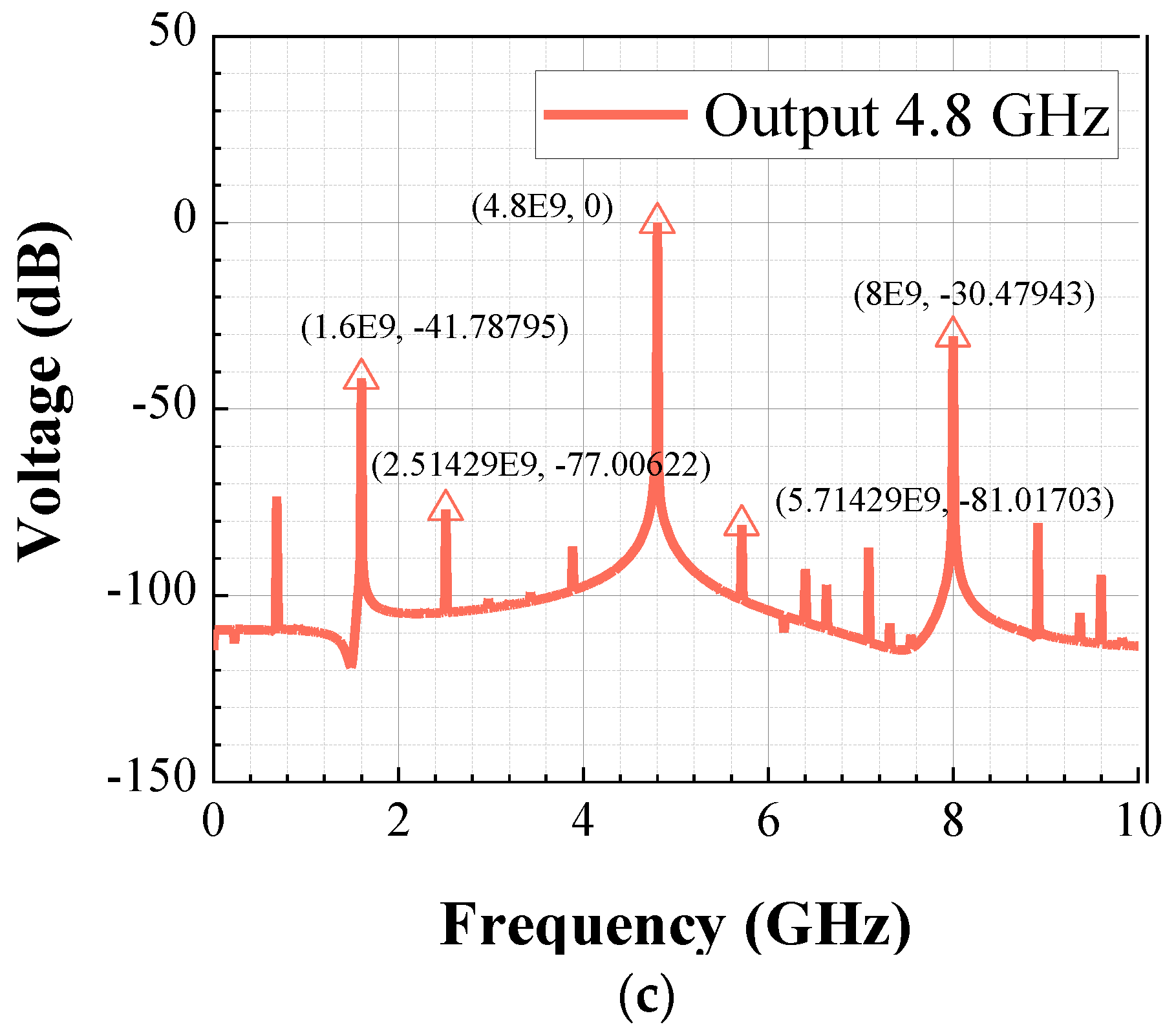
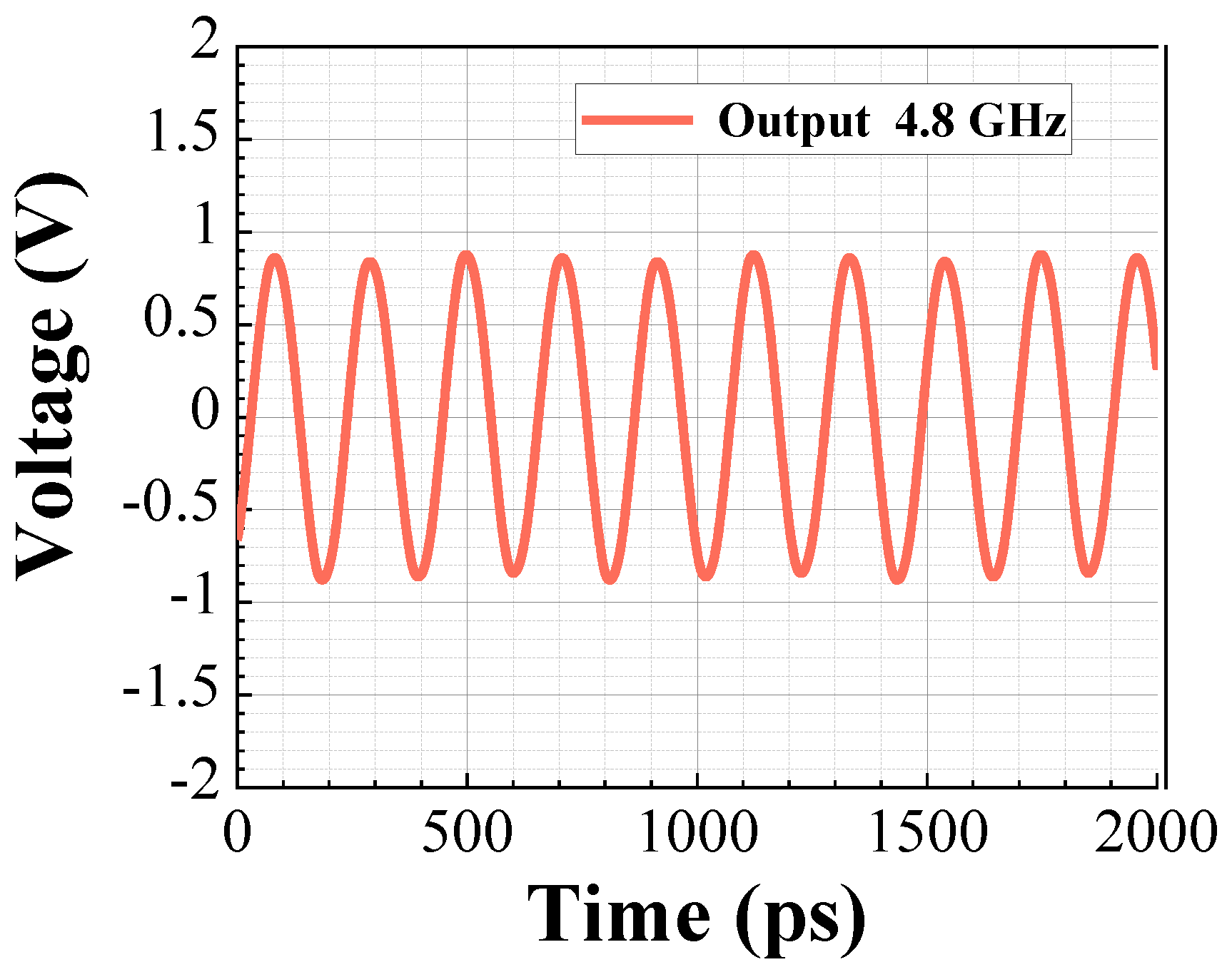
Figure 4 displays the transient waveforms of the SSB mixer, which consists of four 1/2
quadrature inputs at the 3.2 GHz frequency, four 1/4
inputs at the 1.6 GHz frequency, and a 3/4
differential output.
As shown in
Figure 5a,b, the third-order and fifth-order harmonics of the SSB mixer outputs are significantly large, which would lead to harmonic mixing and increase the spur levels. The SSB mixer can generate single-sideband down-conversion outputs of 1 ×
/4 at the 1.6 GHz frequency. Moreover, the spectrum appears the outputs of 5 ×
/4 at the 8 GHz frequency due to harmonic mixing between the third-order harmonic of the 1 ×
/4 input and other 1 ×
/2 input.
Figure 5c displays the 4.8 GHz output spectrum, where the SSB mixer achieves a sideband suppression >−42 dBc at the 1.6 GHz frequency, as well as harmonic mixing suppression >−30 dBc at the 8 GHz frequency. However, the spur suppression is still poor, even with the inherent characteristic of spur rejecting of the SSB mixer and the LC tank filtering.
Therefore, it is necessary to increase the sideband suppression and harmonic mixing suppression. A current-mode-logic (CML) inductive peaking (IP) circuit is used to solve the spurious problem and achieve efficient LO delivery over a long wire of the multi-mm length.
3.2. Comparison of Long Wires Delivery Circuits
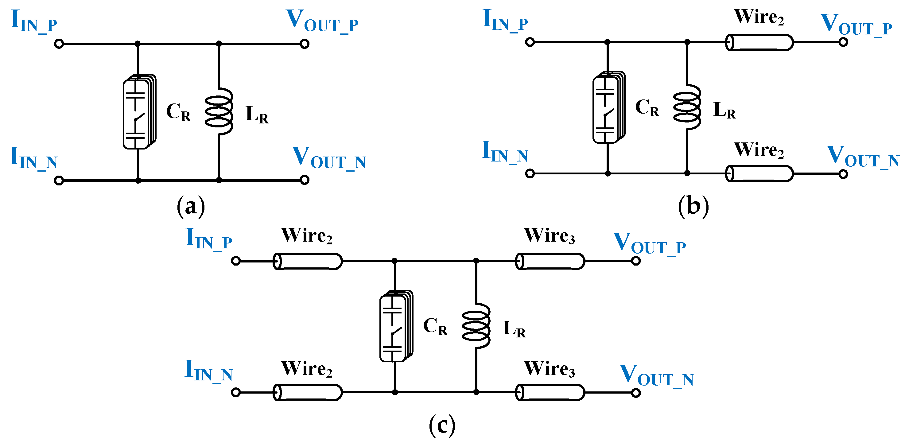
Conventional inductive peaking (IP) topologies are presented in
Figure 6, which includes three topologies, a single shunt IP without long wires as a blank comparison, a single shunt IP with long wires delivery, and a single shunt IP with splitting wires. The IP circuit uses an LC tank to improve noise suppression and voltage headroom. In the architecture of
Section 2, input current mode signals come from the SSB mixer outputs. An inductor is deployed, along with parasitic capacitances and a C bank to form an LC tank, then it would achieve impedance transformation and filtering.
As shown in
Figure 7, the spur levels are partly declined when using traditional single IP topologies, while still suffering from limited driving capacity. The limitation of the single IP architecture lies in the long wires with large capacitance and poor spur levels of the delivery signals. Ideally, the outputs of the SSB mixer only produce a single tone, but the harmonic mixing components of the SSB mixer are large, and the SSB mixer itself also has phase/amplitude imbalance and leakage signals due to design and fabrication mismatch. Therefore, the output spectrum of the SSB mixer may appear to have undesirable frequency components. Even if the LC tank can suppress undesirable spurious tones, it is still poor because of the tradeoff between the bandwidth and the sideband suppression. In addition, it is necessary to overcome the obstacle to deliver large-swing signals over long wires of the multi-mm length.
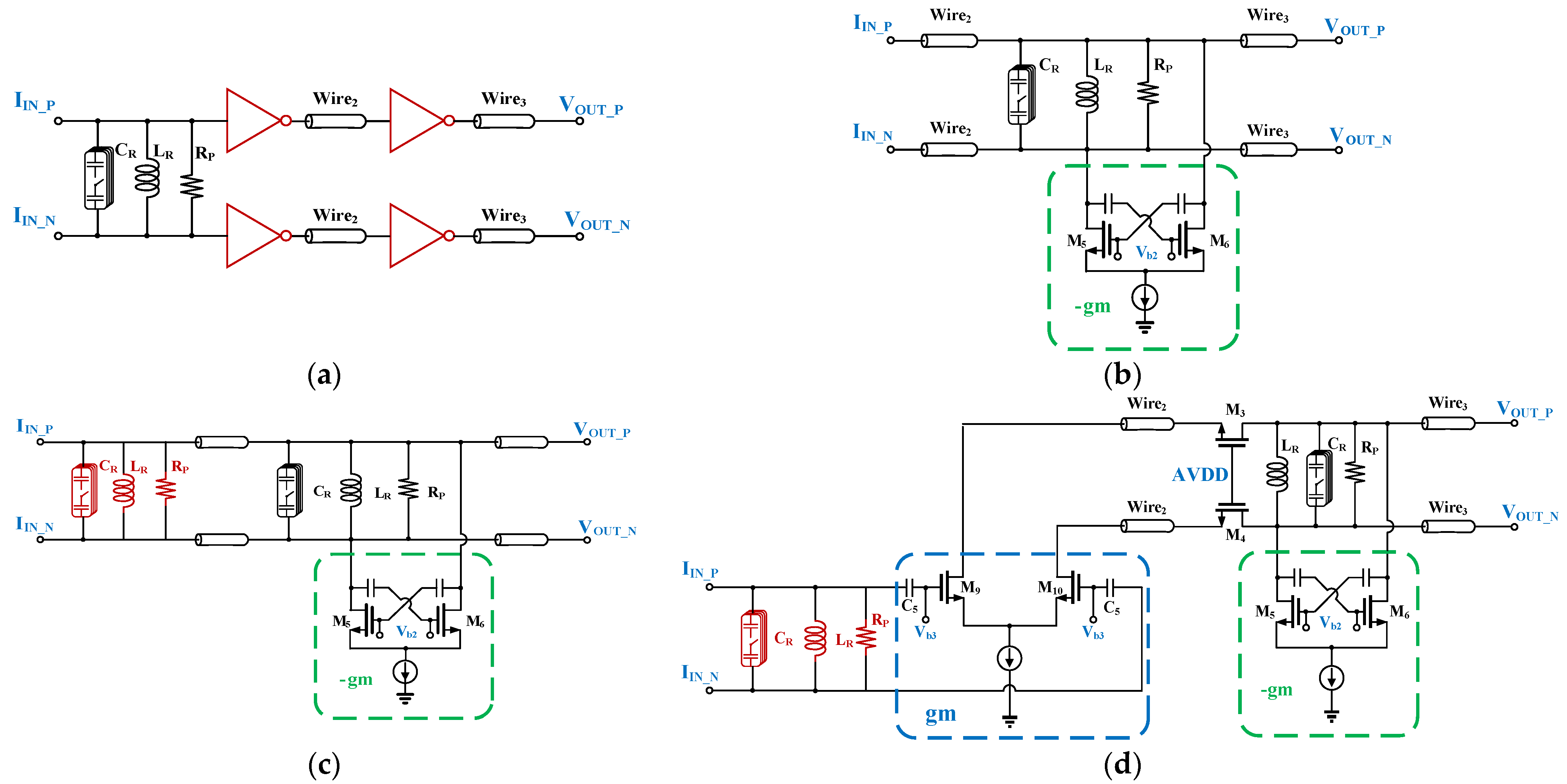
The low spur levels and high efficiency are desirable characteristics for LO delivery circuits. Previous circuit techniques focused on reducing spur by using a single IP circuit. This section presents four different types of LO delivery circuits by combining the IP technique with other improving spur level techniques, then we conclude the critical performance. We assume that an LC tank includes an ideal inductor, an ideal capacitor, and an equivalent parallel resistor.
As shown in
Figure 8a, an inverter-based IP topology is employed to drive a large capacitive load of long wires, which are split into several wires and driven by multiple inverters. Before inverters and long wires, an IP circuit is used to filter out spurious tones. This type of LO delivery takes advantage of simple design and compact area. However, it is difficult to drive long wires of the multi-mm length, since it needs larger sizes of transistors and more power to deliver LO signals as the length of long wires increases. Then, the RC delay from parasitic capacitance and resistance of the large transistors, as well as the capacitive impedance of the long wires would harm high-speed LO signals. Thus, the inverter-based IP topology suffers from the difficulty of extreme power consumption.
Figure 8b describes a topology that combines the IP circuit with an active negative gm (-gm) boosting [
25]. By using an active -gm load, the gain of the differential LO signals increases, and it also adopts a splitting-wires IP circuit to suppress spurious tones. However, the topology also suffers from the problem of limited spur suppression. To improve the capacity of spur suppression, dual-IP circuits are utilized in
Figure 8c. The dual-IP circuits with active -gm boosting can alleviate the stress of the voltage gain and spur suppression, but the bandwidth of the LO delivery circuit would be degraded, when it is needed to drive high-speed long wires. Since it uses voltage mode to deliver LO signals, the LO delivery topology in
Figure 8d is an alternative, which employs a CML-IP circuit using distribution cascode and active -gm boosting. A CML-IP driver is added to the input end of the long wire; thus, a high-speed LO signal can be delivered by the mode of current not voltage, which can achieve wideband even considering the large parasitic capacitance of the long wires. In addition, a pair of differential cascode transistors and an IP circuit with active -gm boosting is used to split long wires. Therefore, this topology can reduce the spur suppression by dual inductive peaking as well as gain-boosting by a distribution cascode amplifier and an active load.
As shown in
Figure 9, output voltage swings of four LO delivery topologies are controlled as identical values to achieve a reasonable comparison of the performance. As shown in
Figure 10, all four topologies can improve spur suppression, and the topology of distribution-cascode-based CML-IP even can improve spur suppression up to 30 dBc.
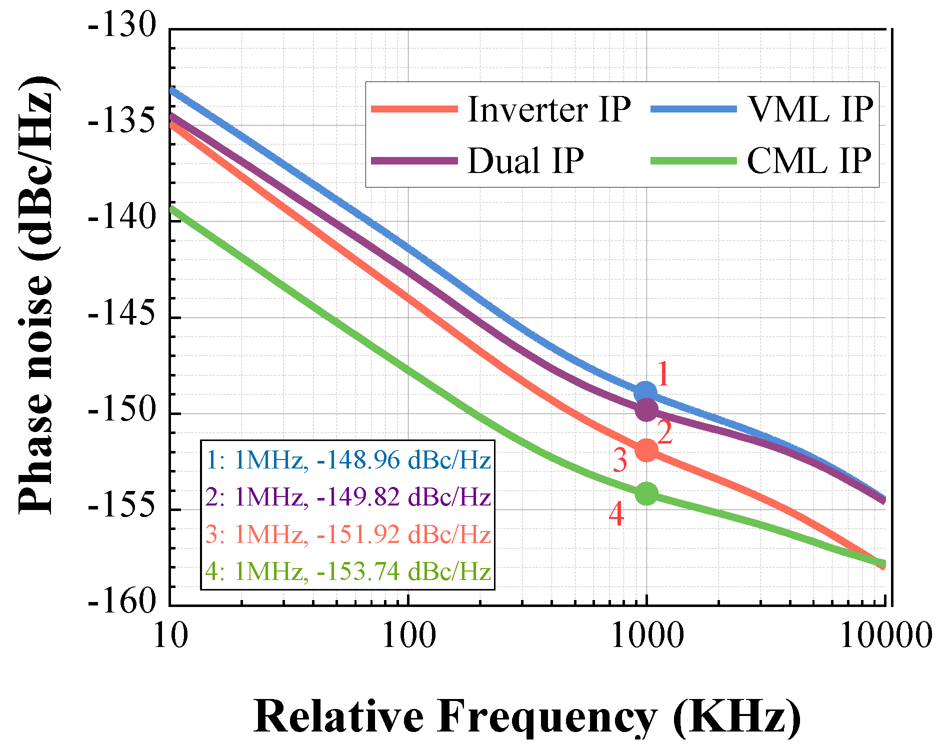
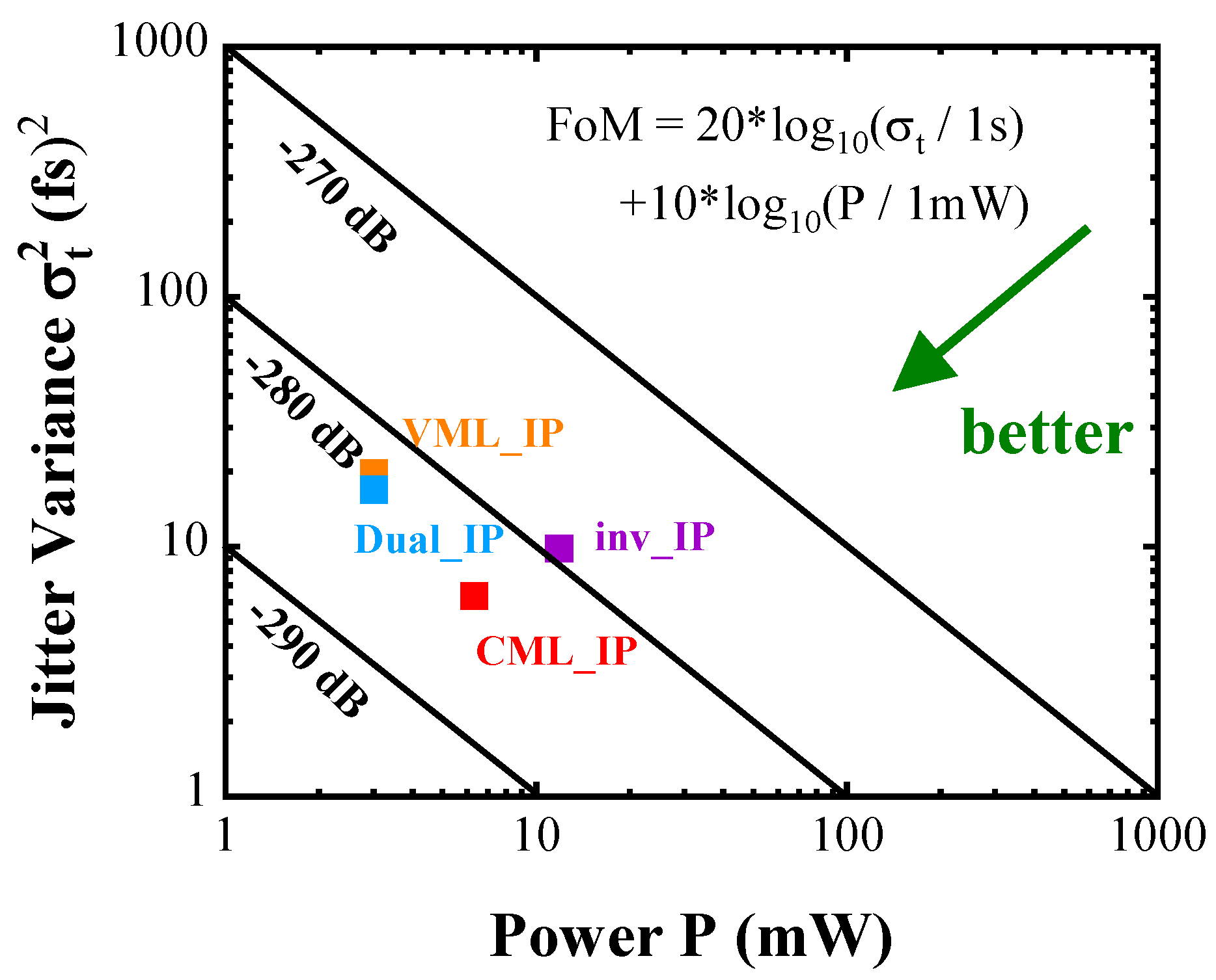
Figure 11 shows the phase noise comparison of four topologies. At the frequency of 4.8 GHz, the CML-IP circuit achieves −153.8 dBc/Hz of phase noise at 1 MHz frequency offset, which is greater than the other three LO delivery topologies. Considering the RMS jitter in the integration range of 10 KHz to 10 MHz and DC Power consumption, the figure of merit (FoM) [
26] is calculated by the following equation:
where
is RMS jitter and
is DC power consumption; FoM is shown in
Figure 12. The performance of four topologies of LO delivery is presented in
Table 1, which also includes the supply-noise-induced jitter (ps) [
27,
28], where a 100 mV peak-to-peak sine wave is added to the supply voltage to simulate the supply noise; then, we calculate the RMS jitter in the integration range of 10 KHz to 10 MHz.
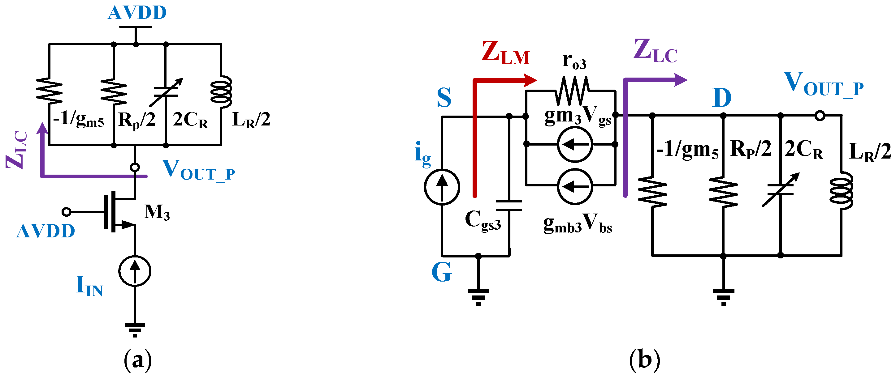
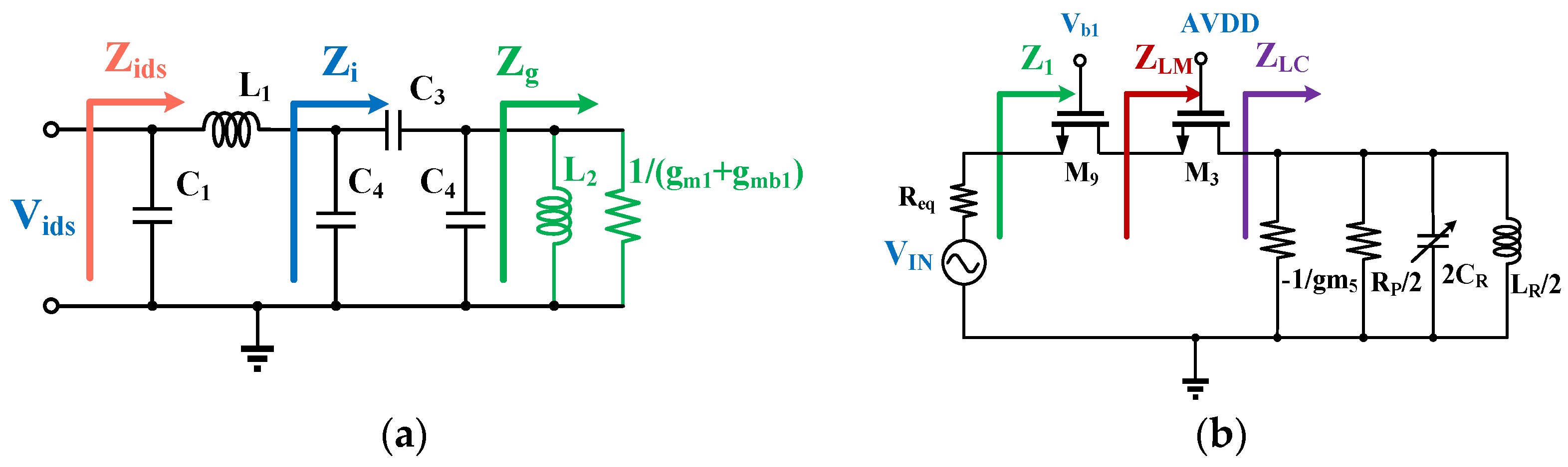
3.3. LO Delivery of Distribution-Cascode-Based CML-IP
Figure 13 shows the distribution-cascode-based CML inductive peaking (IP) circuit for VCO mode, which includes an SSB mixer and a CML-IP delivery circuit.
SSB mixer can generate fractional-N frequency output signals to avoid frequency pulling of the VCO and PA. However, the SSB mixer would result in high spurious tones due to harmonic mixing, imbalance, leakage signals, and some other non-idealities. To improve spur suppression and avoid attenuating signals when LO signals are delivered over long wires, a CML-IP circuit is used to provide large load impedance at the resonant frequency and filter out spurious tones. CML-IP delivery circuit obtains the optimum performance, such as spur suppression, phase noise, supply-noise-induced jitter, and FoM among four LO delivery circuits.
In terms of simulation results, the outputs of the delivery circuit are needed to provide voltage signals above 1 V voltage peak-to-peak (VPP) swing, to drive the following quadrature divider. Therefore, the CML-IP delivery circuit requires a large gain to drive long wires and improve spur suppression of the LO signals from the SSB mixer outputs. However, the gain of the CML-IP circuit is related to the delivery current and load impedance. An LC tank uses a capacitor bank to adjust the resonant frequency of the load impedance to avoid gain degrading.
The following part provides the analysis of the optimum load impedance and current distribution of the CML-IP delivery circuit. The one-port circuit diagram of the CML-IP circuit is shown in
Figure 14a; -gm boosting is equivalent to a negative impedance
. Limited Q-factor of the LC tank is considered as an equivalent shunt resistive impedance, and
,
and
represent the capacitive and inductive components of the LC tank, respectively.
The one-port equivalent model of CML-IP circuit adopts distribution cascode with IP circuit and -gm-boosting, which is presented in
Figure 14b. The load impedance of the cascode transistor
at the output node can be written as:
where
and
represent the load impedance seen from the drain node and the source node of the transistor
, respectively, which is expressed as follows:
Based on the load impedance analysis, the gain of the CML-IP circuit with -gm-boosting can be derived as follows:
At the peak resonant frequency
, the load impedance
can be approximately written as:
where
Q represents the quality factor of the LC tank. According to the small-signal model, the gain of the CML-IP circuit with -gm-boosting is the product of load impedance of the transistor of
output and gm of common source transistor
, which can be derived as:
Considering the large intrinsic gain of one transistor,
Therefore, the gain
can be described as follows:
The gain is related to the positive gm transistor
and negative gm transistor
, and the relation of output voltage swing and positive gm current is illustrated in
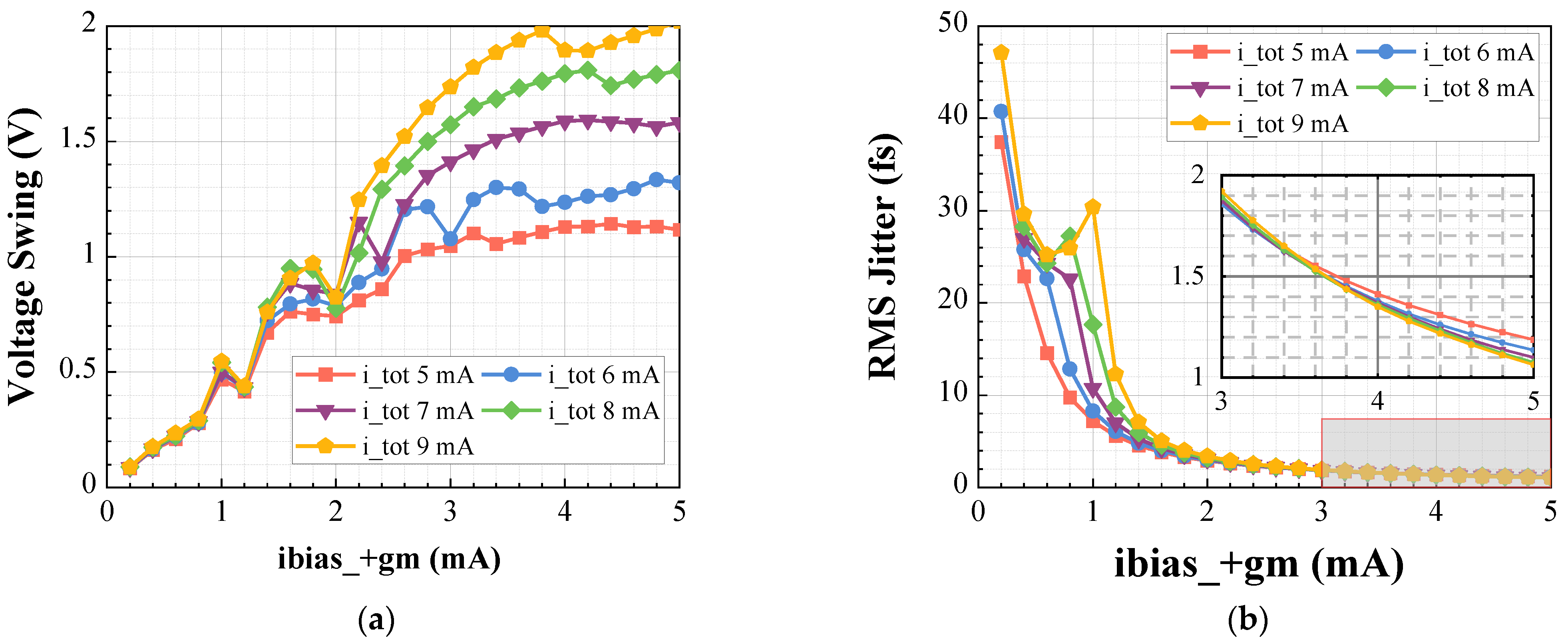
Figure 15a.
Figure 15b,c show the optimum size of the cascode transistor, which presents the tradeoff between output voltage swing and RMS jitter concerning the ratio of width to length (W/L) of the transistor
.
Figure 16 shows the effect of the current distribution between positive gm
and negative gm
on the output voltage swing and RMS jitter. It is necessary to distribute adequate currents to positive gm as much on the condition of limited total currents; more positive gm currents would improve the voltage gain and RMS jitter.
3.4. Load Resuing of Bypass Mode
To independently measure the quadrature LO-generator, the internal VCO is power-off and an external VCO is used as the input for bypass mode.
Figure 17 presents the schematic of a differential common gate-based (CG) clock receiver. Followed by an off-chip Balun, a single-ended clock source at the frequency of 4.8 GHz is transformed to differential signals. The differential input mode and a lower input frequency of external VCO can alleviate the issue of ground bounce due to the inductor and capacitor of the bonding wire and suppress the common-mode noise [
29]. However, the off-chip balun would cause a large in-phase/quadrature-phase (I/Q) imbalance of the clock signal, and the I/Q phase imbalance would appear on the quadrature LO signals at the output node. However, the differential amplifier naturally suppresses this I/Q imbalance, since the phase imbalance is considered as common-mode noise.
Similarly, the clock signal from external VCO is required to deliver over a long wire of a multi-mm length. Thus, the CML-IP delivery circuit is also adapted to obtain high spur suppression and improve phase noise. Moreover, a load reusing technique is used in the clock receiver, which would enhance gain and shrink the chip area.
A one-port equivalent circuit of clock receiver for bypass mode is shown in
Figure 18. We present the analysis of the input impedance and gain of the clock receiver as follows.
The input impedance
of the clock receiver can be written as:
where
is
where
is
At the resonant frequency,
is expressed as:
A similar analysis to VCO mode is presented as follows. The gain of the clock receiver for bypass mode consists of output load impedance and transconductance of the input common-gate transistor.
where
represents output impedance, according to the supposed large intrinsic gain,
The gain of the clock receiver is expressed as follows:
The quadrature LO-generator provides reconfigurable selections of the clock source, either VCO mode or bypass mode which supports the external VCO source.
Figure 19 presents three methods to switch on/off. The switching scheme demands maintaining LO signal integrity for bypass mode and reducing the effect of long wires of external clock delivery on VCO mode. As shown in
Figure 19a, the input common-gate transistors are reused as amplifying and switching. The circuit design is simple and the chip area is compact.
Figure 19b presents the architecture of splitting-wire using a pair of series switching transistors, which isolates the long wires
and the circuits of VCO mode. To further improve the isolation,
Figure 19c adds a switch gm circuit, which would induce the LO signals to the ground when bypass mode is switching off, and it would consume more power due to adding an extra switch gm circuit. Therefore, the switching scheme of
Figure 19b is adopted to reconfigure selections of the clock source, either VCO mode or bypass mode which supports the external VCO source.
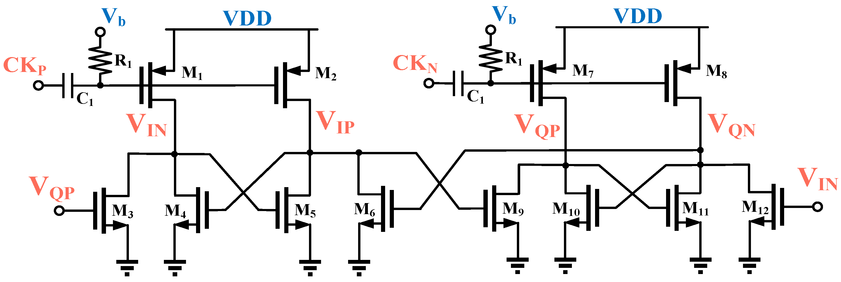
3.5. Quadrature Divide-by-Two Divider
Figure 20 shows the quadrature divider circuit with a regenerative loop, which consists of two latches based on regenerative loops to generate successive four-phased quadrature outputs [
30]. When either one of the input signals turns high, the associated branches are off. For example,
is assumed to turn high, then M11 and M12 are off and the associated outputs of the
and
obtain low. Similarly, when either one of the input signals turns low, the related branches turn on; for example, when
turns low, it is assumed that
turns on, then
keeps low, and
and
also hold low, otherwise, it would violate the initial assumption of
turning on. Four-phased outputs alternately turn high during two periods; thus, the quadrature divider generates divide-by-two signals with the 25% duty cycle.
4. Simulation Results and Discussion
The proposed quadrature LO-generator was designed with 55 nm CMOS technology. All circuits are designed and simulated on Virtuoso Design Environment.
Figure 21 shows the layout of four main circuit blocks, consisting of an SSB mixer with a positive gm circuit, a distribution cascode using CML-IP technique with a negative gm-boosting, a quadrature divide-by-two divider, and a clock receiver for bypass mode supporting external VCO input.
Figure 22 shows the simulated timing waveforms of the critical nodes of the proposed quadrature LO-generator for the VCO mode and the bypass mode, respectively.
Figure 22a,b display the transient waveforms for VCO mode. The VCO generates differential signals at the inputs of the quadrature LO-generator; the differential signals achieve 3.2 V voltage peak-to-peak (VPP) swing at the 6.4 GHz frequency. Then, the 4.8 GHz outputs of the SSB mixer are desired to deliver CML signals over long wires and produce voltage signals as the inputs of the quadrature divider. The cascode output signals indicate that the CML-IP delivery circuit has effectively overcome the deterioration of parasitic capacitance of long wires.
Figure 22c presents transient waveforms at key nodes for bypass mode. An external clock at the 4.8 GHz frequency is converted from the single-ended signal to differential signals through an off-chip balun. The common-gate amplifier of the clock receiver achieves impedance matching and amplifying. In addition, the CML-IP circuit for VCO mode is reused as a common load for bypass mode.
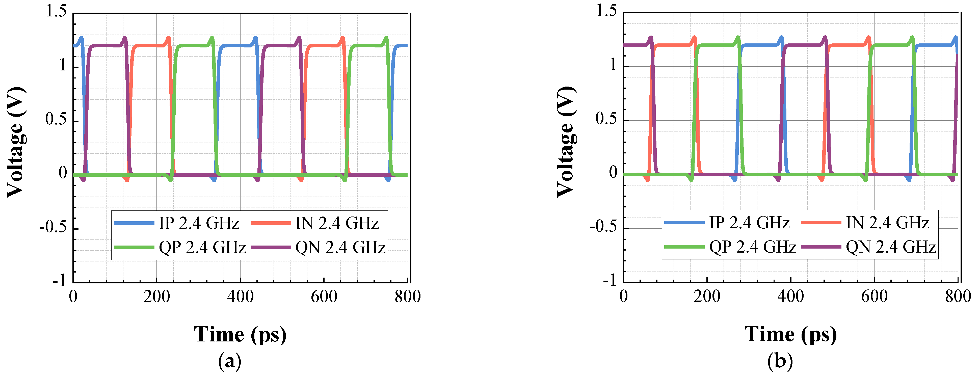
Figure 23 displays the transient waveforms of the quadrature LO outputs at the 2.4 GHz frequency, presenting the simulated results and post-layout simulation results.
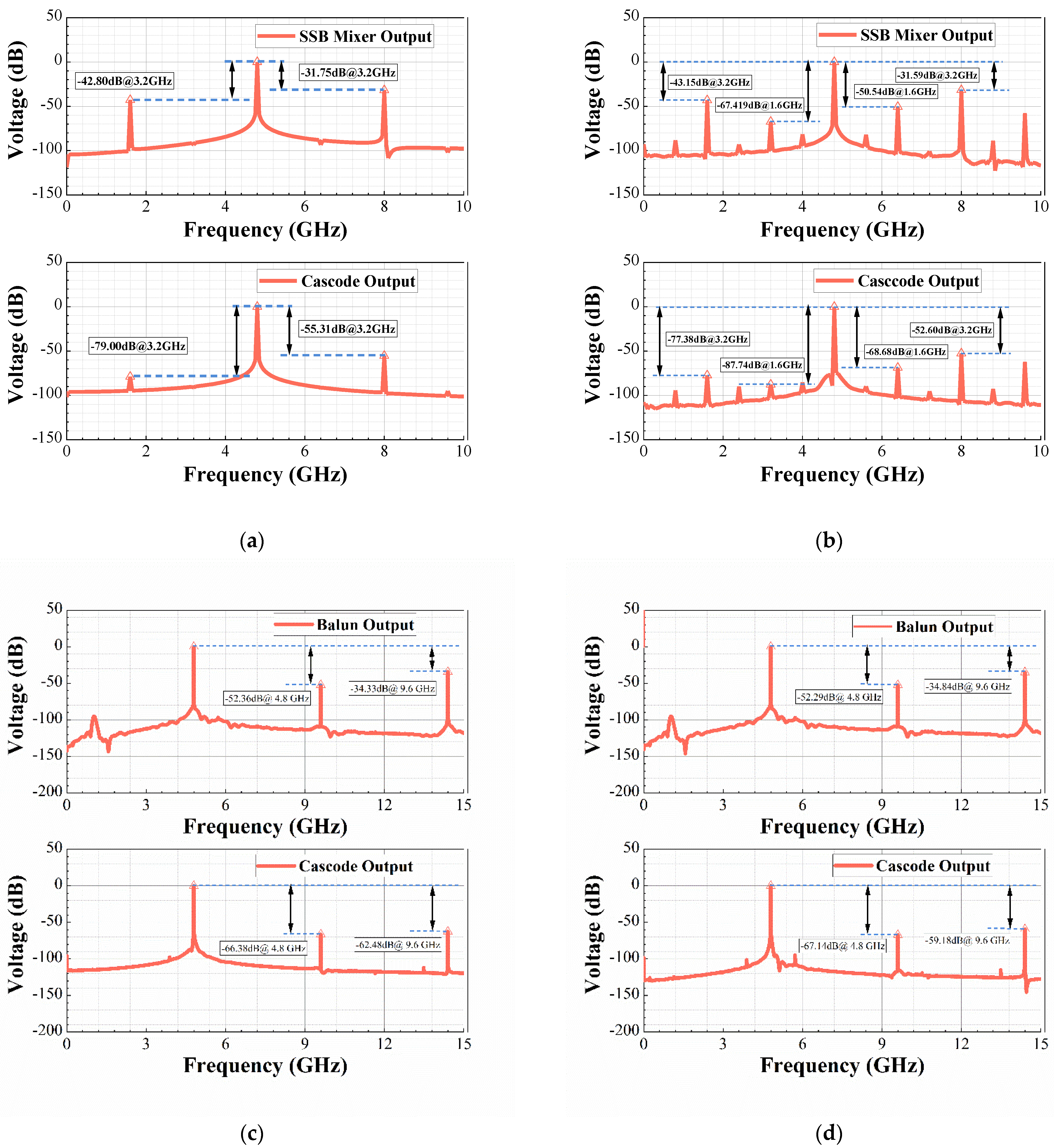
As shown in
Figure 24a,b, the spectra are normalized to the fundamental signal at the 4.8 GHz frequency. When the quadrature LO-generator operates at VCO mode, the spur levels from the SSB mixer outputs to cascode outputs have been significantly decreased. For the 8 GHz mixing harmonics component, the CML-IP delivery circuit presents spur reduction over 23.5 dBc of simulated results and 21.0 dBc of post-layout simulation results. For the 1.6 GHz lower sideband component, the CML-IP delivery circuit presents spur reduction over 36.2 dBc of the simulated results and 34.23 dBc of the post-layout simulation results. Therefore, the CML-IP delivery circuit achieves efficient sideband suppression and mixing harmonics suppression.
Similarly, when the quadrature LO-generator operates at bypass mode from an external clock source, spurious tones are also suppressed due to the CML-IP circuit. The third-order harmonic suppressions of simulated results and post-layout simulation results are improved from −36 dBc to −66 dBc, as well as from −37 dBc to −61 dBc, respectively. The spectrum displays the third-order harmonic rejection over 28 dBc and 24 dBc, respectively. Moreover, second-order harmonic components of simulated results and post-layout simulation are reduced over 14 dBc and 15 dBc, respectively.
Figure 25 shows the simulation results of the S-parameters of the clock receiver, which achieve great impedance matching over the desired band.
Figure 25b presents the results of
, which attains gain over 10 dB at the frequency of 4.8–5 GHz by adjusting the critical code of the capacitor bank to achieve adequate gain.
At the 1 MHz frequency offset, which is relative to the 4.8 GHz frequency carrier,
Figure 26 presents the phase noise results of the quadrature LO-generator when operated at either VCO mode or bypass mode.
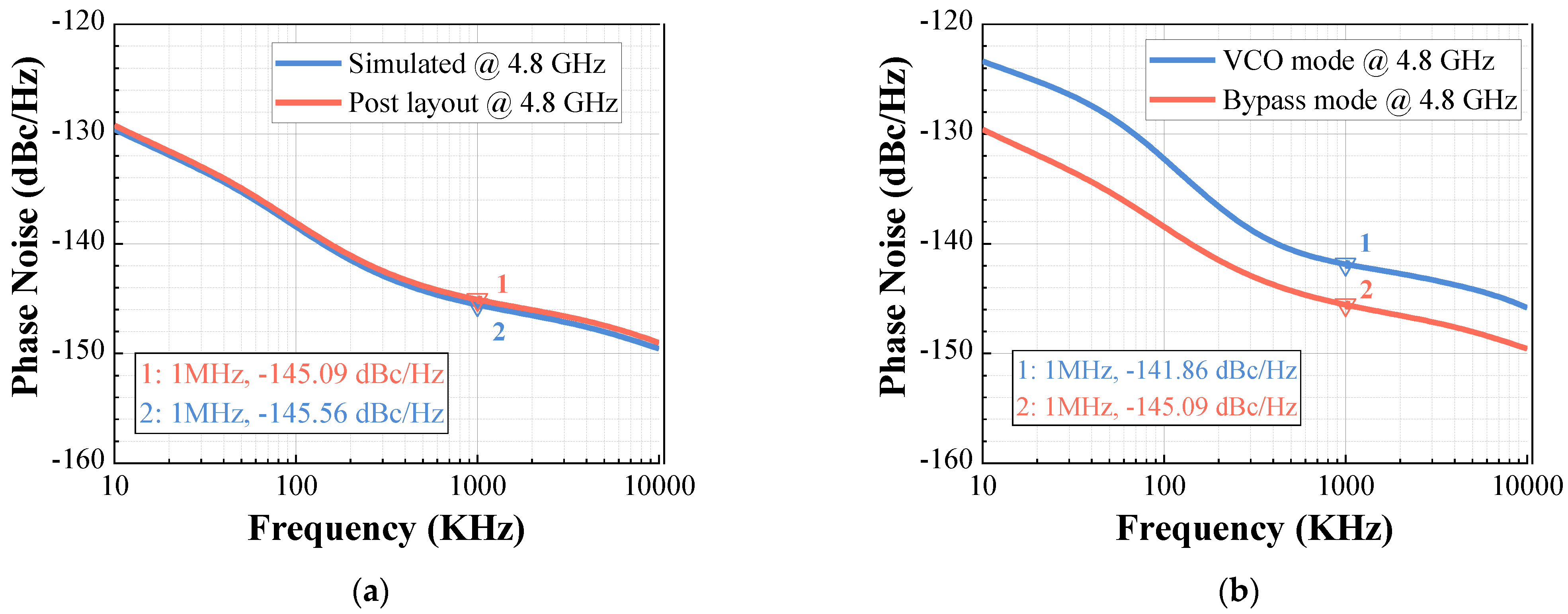
Figure 26a presents the phase noises of simulated results and post-layout simulation results for bypass mode; both phase noise results are approximate. In addition,
Figure 26b compares phase noise results for VCO mode and bypass mode, where the quadrature LO-generator achieves phase noise of −141.86 dBc/Hz and −145.09 dBc/Hz, respectively.
Figure 27 presents the power consumption of the quadrature LO-generator for VCO mode and bypass mode, which consume the total power of 23.86 mW and 15.71 mW, respectively.
Table 2 summarizes and compares the characteristics of the proposed quadrature LO-generator with previously published reports. Our architecture of quadrature LO-generator combines an SSB mixer with a divider to achieve fractional-N frequency planning. The CML-IP delivery circuit is adopted to drive long wires and suppress spur produced from the SSB mixer. Our proposed quadrature LO-generator achieves spur suppression of −52.6 dBc and −59.2 dBc for VCO mode and bypass mode, respectively. Comprehensively considering the power and RMS jitter, the greater FoM of −270.8 and −264.9 for VCO mode and bypass mode can be obtained, respectively.
5. Conclusions
In this paper, a novel quadrature LO-generator using a fractional-N frequency architecture for WLAN application is proposed, in which fractional-N frequency planning is achieved by a single-sideband (SSB) mixer and multiple dividers to avoid the frequency pulling and alleviate the self-mixing and DC offset issues. To improve phase noise and suppress spurious tones of LO signals due to harmonic mixing, imbalance, and leakage of the SSB mixer, four types of LO delivery circuits using the iductive peaking (IP) technique were proposed and compared. Among the four circuits, the CML-IP delivery circuit achieves the optimum performance in terms of spur suppression, phase noise, and capacity of driving long wires. In addition, the quadrature LO-generator can achieve two alternatives of the input clock source, either at VCO mode or at bypass mode supporting external VCO input. Compared to previous digital spur cancellation methods, the CML-IP circuit displays greater performance. For VCO mode and bypass mode, the simulation results demonstrate spur suppression of −52.6 dBc and −59.2 dBc, respectively; phase noise of −142 dBc/Hz and −145.09 dBc/Hz at 1 MHz offset at the 4.8 GHz carrier frequency, respectively; and FoM of −271 and −264.9, respectively. Nevertheless, the proposed quadrature LO-generator may suffer from gain degradation as the length of long wires of LO delivery increases. Therefore, future research is needed to improve the ability of dynamic adaption for LO delivery length.
Author Contributions
Conceptualization, T.T., P.L., H.H. and Y.P.; methodology, T.T., P.L., H.H. and Y.P.; software, T.T., P.L., H.H. and Y.P.; validation, T.T., P.L., H.H. and Y.P.; formal analysis, T.T., P.L., H.H. and Y.P.; writing—original draft preparation, T.T.; writing—review and editing, T.T., P.L., H.H. and Y.P.; supervision, B.W.; funding acquisition, B.W. All authors have read and agreed to the published version of the manuscript.
Funding
This research was funded by the National Major Science and Technology Program of China grant number 2013ZX03004007.
Conflicts of Interest
The authors declare no conflict of interest.
References
- Izad, M.M.; Heng, C. A Pulse Shaping Technique for Spur Suppression in Injection-Locked Synthesizers. IEEE J. Solid-State Circuits 2012, 47, 652–664. [Google Scholar] [CrossRef]
- Arasu, M.A.; Ong, H.K.F.; Yeung Bun, C.; Wooi Gan, Y. A 2.4-GHz CMOS RF front-end for wireless sensor network applications. In Proceedings of the IEEE Radio Frequency Integrated Circuits (RFIC) Symposium, San Francisco, CA, USA, 10–13 June 2006; p. 4. [Google Scholar]
- Kaukovuori, J.; Stadius, K.; Ryynanen, J.; Halonen, K.A.I. Analysis and Design of Passive Polyphase Filters. IEEE Trans. Circuits Syst. I Regul. Pap. 2008, 55, 3023–3037. [Google Scholar] [CrossRef]
- Huang, D.; Li, W.; Zhou, J.; Li, N.; Chen, J. A Frequency Synthesizer with Optimally Coupled QVCO and Harmonic-Rejection SSBmixer for Multi-Standard Wireless Receiver. IEEE J. Solid-State Circuits 2011, 46, 1307–1320. [Google Scholar] [CrossRef]
- Ullah, F.; Liu, Y.; Li, Z.; Wang, X.; Sarfraz, M.M.; Zhang, H. A Bandwidth-Enhanced Differential LC-Voltage Controlled Oscillator (LC-VCO) and Superharmonic Coupled Quadrature VCO for K-Band Applications. Electronics 2018, 7, 127. [Google Scholar] [CrossRef] [Green Version]
- Simon, M.; Laaser, P.; Filimon, V.; Geltinger, H.; Friedrich, D.; Raman, Y.; Weigel, R. An 802.11a/b/g RF Transceiver in an SoC. In Proceedings of the 2007 IEEE International Solid-State Circuits Conference, San Francisco, CA, USA, 11–15 February 2007; pp. 562–622. [Google Scholar]
- Bajestan, M.M.; Rezaei, V.D.; Entesari, K. A Low Phase-Noise Wide Tuning-Range Quadrature Oscillator Using a Transformer-Based Dual-Resonance Ring. IEEE Trans. Microw. Theory Tech. 2015, 63, 1142–1153. [Google Scholar] [CrossRef]
- Yoon, H.; Lee, Y.; Lim, Y.; Tak, G.; Kim, H.; Ho, Y.; Choi, J. A 0.56–2.92 GHz Wideband and Low Phase Noise Quadrature LO-Generator Using a Single LC-VCO for 2G–4G Multistandard Cellular Transceivers. IEEE J. Solid-State Circuits 2016, 51, 614–625. [Google Scholar] [CrossRef]
- Zanuso, M.; Levantino, S.; Samori, C.; Lacaita, A.L. A Wideband 3.6 GHz Digital ΔΣ Fractional-N PLL With Phase Interpolation Divider and Digital Spur Cancellation. IEEE J. Solid-State Circuits 2011, 46, 627–638. [Google Scholar] [CrossRef]
- Temporiti, E.; Weltin-Wu, C.; Baldi, D.; Tonietto, R.; Svelto, F. A 3 GHz Fractional All-Digital PLL With a 1.8 MHz Bandwidth Implementing Spur Reduction Techniques. IEEE J. Solid-State Circuits 2009, 44, 824–834. [Google Scholar] [CrossRef]
- Phan, A.T.; Lee, J.; Krizhanovskii, V.; Le, Q.; Han, S.; Lee, S. Energy-Efficient Low-Complexity CMOS Pulse Generator for Multiband UWB Impulse Radio. IEEE Trans. Circuits Syst. I Regul. Pap. 2008, 55, 3552–3563. [Google Scholar] [CrossRef]
- Borremans, J.; Vengattaramane, K.; Giannini, V.; Craninckx, J. A 86MHz-to-12GHz digital-intensive phase-modulated fractional-N PLL using a 15pJ/Shot 5ps TDC in 40nm digital CMOS. In Proceedings of the 2010 IEEE International Solid-State Circuits Conference (ISSCC), San Francisco, CA, USA, 7–11 February 2010; pp. 480–481. [Google Scholar]
- Song, T.; Oh, H.; Yoon, E.; Hong, S. A Low-Power 2.4-GHz Current-Reused Receiver Front-End and Frequency Source for Wireless Sensor Network. IEEE J. Solid-State Circuits 2007, 42, 1012–1022. [Google Scholar] [CrossRef]
- Dave, M.; Jain, M.; Baghini, M.S.; Sharma, D. A Variation Tolerant Current-Mode Signaling Scheme for On-Chip Interconnects. IEEE Trans. Very Large Scale Integr. VLSI Syst. 2013, 21, 342–353. [Google Scholar] [CrossRef]
- Mensink, E.; Schinkel, D.; Klumperink, E.A.M.; Tuijl, E.v.; Nauta, B. Power Efficient Gigabit Communication Over Capacitively Driven RC-Limited On-Chip Interconnects. IEEE J. Solid-State Circuits 2010, 45, 447–457. [Google Scholar] [CrossRef]
- Hannan, M.A.; Abbas, S.M.; Samad, S.A.; Hussain, A. Modulation Techniques for Biomedical Implanted Devices and Their Challenges. Sensors 2012, 12, 297–319. [Google Scholar] [CrossRef] [Green Version]
- Chia-Hsin, W.; Chih-Hun, L.; Wei-Sheng, C.; Shen-Iuan, L. CMOS wideband amplifiers using multiple inductive-series peaking technique. IEEE J. Solid-State Circuits 2005, 40, 548–552. [Google Scholar] [CrossRef]
- Li, H.; El-Gabaly, A.M.; Saavedra, C.E. A Low-Power Low-Noise Decade-Bandwidth Switched Transconductor Mixer With AC-Coupled LO Buffers. IEEE Trans. Circuits Syst. I Regul. Pap. 2018, 65, 510–521. [Google Scholar] [CrossRef]
- Chen, D.; Yeo, K.S.; Shi, X.; Do, M.A.; Boon, C.C.; Lim, W.M. Cross-Coupled Current Conveyor Based CMOS Transimpedance Amplifier for Broadband Data Transmission. IEEE Trans. Very Large Scale Integr. VLSI Syst. 2013, 21, 1516–1525. [Google Scholar] [CrossRef]
- Orser, H.; Gopinath, A. A 20 GS/s 1.2 V 0.13 um CMOS Switched Cascode Track-and-Hold Amplifier. IEEE Trans. Circuits Syst. II Express Briefs 2010, 57, 512–516. [Google Scholar] [CrossRef]
- Jeong-Kyoum, K.; Jaeha, K.; Sang-Yoon, L.; Suhwan, K.; Deog-Kyoon, J. A 26.5–37.5 GHz frequency divider and a 73-GHz-BW CML buffer in 0.13μm CMOS. In Proceedings of the 2007 IEEE Asian Solid-State Circuits Conference, Jeju City, Korea, 12–14 November 2007; pp. 148–151. [Google Scholar]
- Koukab, A.; Yu, L.; Declercq, M.J. A GSM-GPRS/UMTS FDD-TDD/WLAN 802.11a-b-g multi-standard carrier generation system. IEEE J. Solid-State Circuits 2006, 41, 1513–1521. [Google Scholar] [CrossRef]
- El-Desouki, M.M.; Qasim, S.M.; BenSaleh, M.; Deen, M.J. Single-Chip Fully Integrated Direct-Modulation CMOS RF Transmitters for Short-Range Wireless Applications. Sensors 2013, 13, 9878–9895. [Google Scholar] [CrossRef] [PubMed] [Green Version]
- Ingels, M.; Soens, C.; Craninckx, J.; Giannini, V.; Kim, T.; Debaillie, B.; Libois, M.; Goffioul, M.; Driessche, J.V. A CMOS 100 MHz to 6 GHz software defined radio analog front-end with integrated pre-power amplifier. In Proceedings of the ESSCIRC 2007—33rd European Solid-State Circuits Conference, Munich, Germany, 11–13 September 2007; pp. 436–439. [Google Scholar]
- Drake, A.J.; Nowka, K.J.; Nguyen, T.Y.; Burns, J.L.; Brown, R.B. Resonant clocking using distributed parasitic capacitance. IEEE J. Solid-State Circuits 2004, 39, 1520–1528. [Google Scholar] [CrossRef]
- Wu, W.; Yao, C.W.; Guo, C.; Chiang, P.Y.; Lau, P.K.; Chen, L.; Son, S.W.; Cho, T.B. 32.2 A 14nm Analog Sampling Fractional-N PLL with a Digital-to-Time Converter Range-Reduction Technique Achieving 80fs Integrated Jitter and 93fs at Near-Integer Channels. In Proceedings of the 2021 IEEE International Solid- State Circuits Conference (ISSCC), San Francisco, CA, USA, 13–22 February 2021; pp. 444–446. [Google Scholar]
- Strak, A.; Gothenberg, A.; Tenhunen, H. Power-Supply and Substrate-Noise-Induced Timing Jitter in Nonoverlapping Clock Generation Circuits. IEEE Trans. Circuits Syst. I Regul. Pap. 2008, 55, 1041–1054. [Google Scholar] [CrossRef]
- Wang, X.J.; Kwasniewski, T. Propagation Delay-Based Expression of Power Supply-Induced Jitter Sensitivity for CMOS Buffer Chain. ITElC 2016, 58, 627–630. [Google Scholar] [CrossRef]
- Tian, T.; Li, P.; Huang, H.-Q.; Wu, B. A quadrature LO-generator using an external single-ended clock receiver for dual-band WLAN applications. IEICE Electron. Express 2021, 18, 20210130. [Google Scholar] [CrossRef]
- Razavi, B.; Lee, K.F.; Yan, R.H. Design of high-speed, low-power frequency dividers and phase-locked loops in deep submicron CMOS. IEEE J. Solid-State Circuits 1995, 30, 101–109. [Google Scholar] [CrossRef]
Figure 1.
Architecture of proposed quadrature LO-generator.
Figure 1.
Architecture of proposed quadrature LO-generator.
Figure 2.
(a) Block diagram of a single sideband (SSB) up-converter. (b) Typical spectra of an SSB up-converter at input and output nodes.
Figure 2.
(a) Block diagram of a single sideband (SSB) up-converter. (b) Typical spectra of an SSB up-converter at input and output nodes.
Figure 3.
Schematic of the SSB mixer.
Figure 3.
Schematic of the SSB mixer.
Figure 4.
Simulated SSB mixer waveforms: (a) input 3.2 GHz; (b) input 1.6 GHz; (c) output 4.8 GHz.
Figure 4.
Simulated SSB mixer waveforms: (a) input 3.2 GHz; (b) input 1.6 GHz; (c) output 4.8 GHz.
Figure 5.
Simulated SSB mixer spectrum: (a) input 3.2 GHz; (b) input 1.6 GHz; (c) output 4.8 GHz.
Figure 5.
Simulated SSB mixer spectrum: (a) input 3.2 GHz; (b) input 1.6 GHz; (c) output 4.8 GHz.
Figure 6.
Conventional LO delivery topologies: (a) IP technique without long wires; (b) IP technique with long wires; (c) IP technique with splitting-long wires.
Figure 6.
Conventional LO delivery topologies: (a) IP technique without long wires; (b) IP technique with long wires; (c) IP technique with splitting-long wires.
Figure 7.
Spectrums of conventional LO delivery topologies: (a) IP technique without long wires; (b) IP technique with long wires; (c) IP technique with splitting-long wires.
Figure 7.
Spectrums of conventional LO delivery topologies: (a) IP technique without long wires; (b) IP technique with long wires; (c) IP technique with splitting-long wires.
Figure 8.
Proposed four LO delivery topologies: (a) topology of inverter-based IP; (b) topology of negative gm-boosting-based IP (VML IP); (c) topology of negative gm-boosting-based dual IP (Dual IP); (d) topology of distribution-cascode-based CML-IP.
Figure 8.
Proposed four LO delivery topologies: (a) topology of inverter-based IP; (b) topology of negative gm-boosting-based IP (VML IP); (c) topology of negative gm-boosting-based dual IP (Dual IP); (d) topology of distribution-cascode-based CML-IP.
Figure 9.
Simulated waveform of LO delivery output.
Figure 9.
Simulated waveform of LO delivery output.
Figure 10.
Spur suppression of proposed four LO delivery topologies: (a) topology of inverter-based IP; (b) topology of negative gm-boosting-based IP; (c) topology of negative gm-boosting-based dual IP; (d) topology of distribution-cascode-based CML-IP.
Figure 10.
Spur suppression of proposed four LO delivery topologies: (a) topology of inverter-based IP; (b) topology of negative gm-boosting-based IP; (c) topology of negative gm-boosting-based dual IP; (d) topology of distribution-cascode-based CML-IP.
Figure 11.
Phase noise of proposed four LO delivery topologies at the carrier frequency of 4.8 GHz.
Figure 11.
Phase noise of proposed four LO delivery topologies at the carrier frequency of 4.8 GHz.
Figure 12.
FoM of proposed four LO delivery topologies.
Figure 12.
FoM of proposed four LO delivery topologies.
Figure 13.
Schematic of SSB mixer and LO delivery of CML-IP.
Figure 13.
Schematic of SSB mixer and LO delivery of CML-IP.
Figure 14.
A one-port model of CML-IP with negative gm-boosting: (a) circuit diagram; (b) equivalent circuit.
Figure 14.
A one-port model of CML-IP with negative gm-boosting: (a) circuit diagram; (b) equivalent circuit.
Figure 15.
(a) Effect of positive gm on output voltage swing. Effect of W/L of cascode transistor on: (b) output voltage swing; (c) RMS jitter.
Figure 15.
(a) Effect of positive gm on output voltage swing. Effect of W/L of cascode transistor on: (b) output voltage swing; (c) RMS jitter.
Figure 16.
Effect of current distribution on (a) output voltage swing; (b) RMS jitter.
Figure 16.
Effect of current distribution on (a) output voltage swing; (b) RMS jitter.
Figure 17.
Schematic of bypass mode for external VCO input.
Figure 17.
Schematic of bypass mode for external VCO input.
Figure 18.
A one-port equivalent circuit of: (a) clock receiver for bypass mode; (b) distribution-cascode with negative gm-boosting.
Figure 18.
A one-port equivalent circuit of: (a) clock receiver for bypass mode; (b) distribution-cascode with negative gm-boosting.
Figure 19.
Proposed three bypass switching methods: (a) reusing common-gate transistor and switch transistor; (b) splitting wires using series switch transistor; (c) voltage mode gm switch transistor.
Figure 19.
Proposed three bypass switching methods: (a) reusing common-gate transistor and switch transistor; (b) splitting wires using series switch transistor; (c) voltage mode gm switch transistor.
Figure 20.
Quadrature divide-by-two divider with a regenerative loop.
Figure 20.
Quadrature divide-by-two divider with a regenerative loop.
Figure 21.
Layout of proposed LO-generator and LO delivery: (a) SSB mixer with a positive gm; (b) distribution cascode using CML-IP with a negative gm; (c) quadrature divide-by-two divider; (d) clock receiver for bypass mode of external VCO input.
Figure 21.
Layout of proposed LO-generator and LO delivery: (a) SSB mixer with a positive gm; (b) distribution cascode using CML-IP with a negative gm; (c) quadrature divide-by-two divider; (d) clock receiver for bypass mode of external VCO input.
Figure 22.
Waveforms of LO delivery: (a) simulated results for VCO mode; (b) post-layout simulation results for VCO mode; (c) simulated results and post-layout simulation results for bypass mode.
Figure 22.
Waveforms of LO delivery: (a) simulated results for VCO mode; (b) post-layout simulation results for VCO mode; (c) simulated results and post-layout simulation results for bypass mode.
Figure 23.
Waveforms of output LO signals: (a) simulated results; (b) post-layout simulation results.
Figure 23.
Waveforms of output LO signals: (a) simulated results; (b) post-layout simulation results.
Figure 24.
Spur suppressions of LO delivery: (a) simulated results for VCO mode; (b) post-layout simulation results for VCO mode; (c) simulated results for bypass mode; (d) post-layout simulation results for bypass mode.
Figure 24.
Spur suppressions of LO delivery: (a) simulated results for VCO mode; (b) post-layout simulation results for VCO mode; (c) simulated results for bypass mode; (d) post-layout simulation results for bypass mode.
Figure 25.
S-parameters of clock receiver for bypass mode: (a) S11; (b) S21.
Figure 25.
S-parameters of clock receiver for bypass mode: (a) S11; (b) S21.
Figure 26.
Phase noise of quadrature LO-generator at 4.8 GHz: (a) bypass mode; (b) comparison of VCO mode and bypass mode.
Figure 26.
Phase noise of quadrature LO-generator at 4.8 GHz: (a) bypass mode; (b) comparison of VCO mode and bypass mode.
Figure 27.
Power consumption of quadrature LO-generator: (a) VCO mode; (b) bypass mode.
Figure 27.
Power consumption of quadrature LO-generator: (a) VCO mode; (b) bypass mode.
Table 1.
Performance comparison of proposed four topologies of LO delivery.
Table 1.
Performance comparison of proposed four topologies of LO delivery.
| | Inverter-Based IP | Gm-Boosting-Based IP | Gm-Boosting-Based Dual IP | Distribution-Cascode-Based CML-IP |
|---|
| Spur (dBc) | −40.11 | −31.79 | −30.99 | −53.70 |
Output Voltage
Swing (V) | 1.75 | 1.73 | 1.65 | 1.69 |
| Phase Noise@1 MHz (dBc/Hz) | −151.92 | −148.96 | −149.82 | −154.18 |
| RMS Jitter (fs) | 3.14 | 4.44 | 4.12 | 2.52 |
| PDC (mW) | 11.81 | 3.00 | 3.00 | 6.30 |
| FoM (dB) | −279.34 | −282.28 | −282.93 | −283.98 |
Supply-Noise-Induced
Jitter (ps) | 3.83 | 1.78 | 0.57 | 0.40 |
Table 2.
Performance summary and comparison of quadrature LO-generator.
Table 2.
Performance summary and comparison of quadrature LO-generator.
| | [11] | [9] | [10] | [12] | This |
|---|
| VCO Mode | Bypass Mode |
|---|
| Architecture | On/off switching | Fractional–N divider + Digital Spur Cancellation | Fractional–N counter + Digital Calibration | Fractional–N
Σ-Δ modulator + Digital
Calibration | SSB Mixer + CML-IP |
| CMOS Technology (nm) | 180 | 65 | 65 | 40 | 55 |
| Supply Voltage (V) | 1.5 | 1.2 | 1.2 | - | 1.5 /1.2 |
| LO Frequency (GHz) | 3.1–5.1 | 3–3.6 | 3 | 5.5–12 | 2.4—2.484 |
Phase noise @1 MHz offset
(dBc) @ carrier (GHz) | - | −103.4 @ 3.6 | −123 @ 3 | −144 @ 7 | −141.9 @ 4.8 | −145.6 @ 4.8 |
RMS Jitter (fs)
(Frequency Range) | - | 900
(10 K–30 M) | - | 560
(10 K—40 M) | 11.6
(10 K–10 M) | 6.9
(10 K–10 M) |
| Largest spur (dBc) | −25 | −57 | −45 | −48 | −52.6 | −59.2 |
| Power PDC (mW) | 7.8 | 80 | 10 | 30 | 23.86 | 15.71 |
| * FoM | - | −221 | - | −230 | −270.8 | −264.9 |
| Active Area (mm2) | 0.31 | 0.4 | 0.4 | 0.28 | 0.178 | 0.186 |
| Publisher’s Note: MDPI stays neutral with regard to jurisdictional claims in published maps and institutional affiliations. |
© 2021 by the authors. Licensee MDPI, Basel, Switzerland. This article is an open access article distributed under the terms and conditions of the Creative Commons Attribution (CC BY) license (https://creativecommons.org/licenses/by/4.0/).


