Article

A Novel Low-Area Point Multiplication Architecture for Elliptic-Curve Cryptography

by
Muhammad Rashid
1,
Mohammad Mazyad Hazzazi
2,
Sikandar Zulqarnain Khan
3,*,
Adel R. Alharbi
4,
Asher Sajid
5 and
Amer Aljaedi
4
1
Department of Computer Engineering, Umm Al-Qura University, Makkah 21955, Saudi Arabia
2
Department of Mathematics, College of Science, King Khalid University, Abha 61413, Saudi Arabia
3
Department of Aeronautical Engineering, Estonian Aviation Academy, 61707 Tartu, Estonia
4
College of Computing and Information Technology, University of Tabuk, Tabuk 71491, Saudi Arabia
5
Department of Electrical Engineering, Bahria University, Islamabad 44000, Pakistan
*
Author to whom correspondence should be addressed.
Submission received: 9 September 2021 / Revised: 21 October 2021 / Accepted: 29 October 2021 / Published: 4 November 2021
(This article belongs to the Section Computer Science & Engineering)

Abstract

:
This paper presents a Point Multiplication (PM) architecture of Elliptic-Curve Cryptography (ECC) over G F ( 2 163 ) with a focus on the optimization of hardware resources and latency at the same time. The hardware resources are reduced with the use of a bit-serial (traditional schoolbook) multiplication method. Similarly, the latency is optimized with the reduction in a critical path using pipeline registers. To cope with the pipelining, we propose to reschedule point addition and double instructions, required for the computation of a PM operation in ECC. Subsequently, the proposed architecture over G F ( 2 163 ) is modeled in Verilog Hardware Description Language (HDL) using Vivado Design Suite. To provide a fair performance evaluation, we synthesize our design on various FPGA (field-programmable gate array) devices. These FPGA devices are Virtex-4, Virtex-5, Virtex-6, Virtex-7, Spartan-7, Artix-7, and Kintex-7. The lowest area (433 FPGA slices) is achieved on Spartan-7. The highest speed is realized on Virtex-7, where our design achieves 391 MHz clock frequency and requires 416 μ s for one PM computation (latency). For power, the lowest values are achieved on the Artix-7 (56 μ W) and Kintex-7 (61 μ W) devices. A ratio of throughput over area value of 4.89 is reached for Virtex-7. Our design outperforms most recent state-of-the-art solutions (in terms of area) with an overhead of latency.

1. Introduction

The exponential growth of information technology have resulted in various applications for the betterment of society. Several electronic devices require communicating private data in a secret way [1]. Among many others, cryptography is one technique that is frequently employed to maintain data privacy [2]. It has two types, i.e., symmetric and asymmetric (also termed a public key). The prior contains a single key for encryption or decryption, while a pair of two separate keys (public and private) are required in an asymmetric form. Symmetric algorithms are mainly preferred because of the speed of encryption/decryption as they require fewer computations. Contrarily, the asymmetric algorithms provide high security with additional area/power overheads [1,2]. In asymmetric algorithms, one of the effective approaches to achieving security is Elliptic-Curve Cryptography (ECC). It needs shorter keys to acquire the same security compared with other asymmetric algorithms [3,4,5]. The smaller key sizes ultimately confirms the use of ECC in resource-constrained devices.
To achieve security, there are several applications that demand either software or hardware implementations of ECC. The applications that require software implementations are (i) OpenSSL protocols [6], (ii) bitcoin digital signatures [7], (iii) image encryption/decryption [8,9], and many others. Similarly, the applications that require hardware implementations of ECC are (i) internet of things [10], (ii) radio frequency identification [11,12], (iii) teleoperated robotic systems [13], (iv) network servers [14], and several others. The applications highlighted in [10,11,12,13] require low-cost (or area optimized) implementations. On the other hand, high-speed implementations are required for network related applications where multiple devices want to communicate using a cloud platform. Furthermore, the applications of ECC that require an hardware implementation focus on the speed-up of critical operations.
The mathematical structure of ECC consists of four layers. The uppermost (fourth) layer is the protocol that governs encryption or decryption. The third layer operation, i.e., the point multiplication (PM), also termed scalar multiplication in the literature, is the most time-consuming [14]. The PM execution relies on the computation of the second layer (i.e., point addition (PA) and doubling (PD)) operations. Subsequently, the finite field arithmetic (layer one) operations, i.e., multiplication, addition, inversion, and squaring, are required to compute PA and PD. Apart from these four layers, ECC involves two bases for the elliptic-curve points (i.e., initial, intermediate, and final) representation, i.e., polynomial and normal. The polynomial basis is selected in this article as it is more suitable for achieving efficient finite field multiplications. A normal basis representation is better in all of those scenarios where frequent squares are required to be implemented. Furthermore, the two available coordinate systems are affine and projective. We selected a projective coordinate system as it requires minimal inversion operations.

1.1. State-of-the-Art PM Architectures

Various efforts have been considered in the literature to improve the performance of ECC in light of different design parameters (throughput and area). Here, the design parameters determine the requirements under which a system is expected to operate. Therefore, some most recent throughput optimized (or high-speed) ECC implementations are reported in [14,15,16,17]. Similarly, area-improving implementations are considered in [18,19,20,21]. Despite the high-speed and low-area designs, a variety of hardware accelerators are available in the literature, where the throughput and area parameters are considered at the same time for implementations [22,23,24].
High-speed/throughput-optimized architectures [14,15,16,17]: The most recent high-speed architecture of ECC over G F ( 2 163 ) and G F ( 2 571 ) is presented in [14]. The high speed is obtained by reducing (i) the computation time for one point multiplication operation and (ii) the required clock cycles. The computation time is decreased by using two multipliers and squarers. The multipliers are modular in nature. The clock cycles are reduced by rescheduling the sequence of PA and PD operations for the Montgomery algorithm. The implementation results are given on a Virtex-7 device. For G F ( 2 163 ) and G F ( 2 571 ) , the availed FPGA slices are 1593 and 5575 and the achieved clock frequencies (in MHz) are 293 and 269, respectively. Moreover, the computation times for one point multiplication operation are 3.68 μ s and 13.87 μ s, respectively. A right-to-left PM algorithm is employed in [15] to perform parallel computations of Frobenius maps and PA operation. To shorten the latency, a rescheduling of PA instructions is proposed. Furthermore, a multiplier accumulator is used to improve the clock frequency. The employed multiplier is pipelined and bit-parallel in nature. Their architecture takes 2.50, 4.09, 5.81, 9.50, and 18.51 μ s for one PM calculation on Xilinx Virtex-5 FPGA over G F 2 163 , G F 2 233 , G F 2 283 , G F 2 409 , and G F 2 571 , respectively. In [16], the high speed is achieved with a combined use of the schoolbook long and Karatsuba multiplication algorithms. It allows for better parallelization while retaining low complexity. Furthermore, the Montgomery PM algorithm is also employed. The implementation results, in terms of execution time for one point multiplication operation, on the Xilinx Virtex-7 device over G F ( P ) with P = 256 is 0.139 ms. For G F ( 2 163 ) , another high-performance architecture is reported in [17]. On Kintex-7 FPGA, their architecture utilizes 2253 slices. Moreover, a 306 MHz clock frequency is achieved. Recently, in [25], two different architectures for Ed25519 (Edwards curve digital signature algorithm) are presented. Both of these architectures provide security that is equivalent to AES-128 (Advance Encryption Standard). On Xilinx Zynq-7020 FPGA, their scheme achieves an improvement of more than 84% compared with the best-reported state-of-the-art implementations.
Area-improved designs [18,19,20,21]: Towards area optimization, a Lopez Dahab-based PM architecture over G F ( 2 163 ) is given in [18]. To reduce clock cycles, a bit-parallel hybrid karatsuba multiplier is employed. The hardware resources are preserved with the use of an Itoh–Tsujii inversion algorithm as it takes only the multiplier and squarer for computation. On the Xilinx Virtex-7 device, their architecture utilizes 3657 slices. Moreover, it takes 25.3 μ s for one PM computation. The performance comparison of different PM algorithms, i.e., basic binary, Frobenius map, and Montgomery, over G F ( 2 163 ) are investigated in [19]. For area optimizations, bit/digit serial multipliers are incorporated for the computation of modular multiplication operations. Furthermore, an 8-bit input–output interface is introduced for use with 8-bit processors (to achieve flexibility) for area-constrained applications. On the Xilinx Virtex-5 device, their architecture requires 0.11 ms for one PM operation and utilizes 473 slices. Low-cost and high-speed PM architectures for Binary Edward Curves (a particular type of ECC curves) are presented in [20]. A low cost is acquired by using one pipelined digit-serial multiplier in the processor data path. For high speeds, three pipelined multipliers are incorporated. The implementation results on the Virtex-5 FPGA device are given for G F ( 2 163 ) and G F ( 2 233 ) . A two-stage pipelined PM architecture over G F ( 2 163 ) to G F ( 2 571 ) using the Montgomery algorithm is published in [21]. To reduce the computation time, a rescheduling of PA and PD instructions is performed. A digit-parallel multiplier is provided to reduce clock cycles with a low area utilization.
Throughput and area tweak circuits [22,23,24,26]: A two-stage pipelining is presented in [22] for the PM acceleration. The pipelining is employed to reduce the critical path. Furthermore, a rescheduling of PA and PD operations is presented to reduce the clock cycles. On Xilinx Virtex-7, their design provides a frequency 369, 357, and 337 MHz over G F ( 2 163 ) , G F ( 2 233 ) , and G F ( 2 283 ) , respectively. The ratio of throughput over area (slices) values are 42.22, 12.37, and 9.45. In [23], an improved radix-2-based interleaved modular multiplication architecture is provided to reduce the time complexity. The performance evaluation of their multiplier architecture is provided on various Xilinx FPGA devices. Moreover, the PM is performed on G F ( P ) with P = 192 , 224, 256, 384, and 521. A segmented pipelined multiplier architecture is given in [24] to accelerate the PM operation. A rescheduling of PA and PD operations is proposed to lower the latency values. Similarly, a configurable distributed memory-based architecture is provided to optimize the speed with a reduced area. An interesting work is found in [26], where three different architectures, i.e., lightweight, area-time efficient, and high-performance, of PM over Curve448 (recommended by NIST to provide 224-bit security over ECC) have been presented. The implementation results are captured on a Xilinx Zynq 7020 FPGA. Their high-performance design increases 12% throughput with the execution of 1219 PM operations per second. Their lightweight PM architecture achieves 250 MHz and saves 96% of resources without any performance reduction. Moreover, their area-time efficient design considers a trade-off between time and the required hardware resources, which results in 48% efficiency improvement with a 52% reduction in hardware resources.
The aforementioned discussion reveals that several optimization techniques, i.e., pipelining (used in [21,22]), algorithmic parallelism (adopted in [15]), segmented modular multipliers (employed in [24]), and bit-parallel multipliers (targeted in [16,18]) have been used in existing architecture to speed up the computation of PM in ECC. The use of bit-serial and digit-serial multipliers, used in [19,20], results in a decrease in hardware resources (area) with a decrease in performance of the architecture (compared with bit-parallel modular multipliers). Therefore, there are numerous area-constrained applications such as internet of things [10], radio frequency identification [11,12], and teleoperated robotic systems [13], that require low-cost hardware architectures to perform PM operation in a reasonable time (latency). Subsequently, this work provides a PM architecture with the consideration of hardware resources.

1.2. Contributions

Our contributions are as follows:
  • Elliptic-curve PM architecture: We present a low-area Elliptic-curve PM architecture over G F ( 2 m ) with m = 163 (descriptions are available in Section 3).
  • Bit-serial polynomial multiplier architecture: For two m-bit polynomial multiplications over G F ( 2 163 ) , we propose a bit serial multiplier architecture for the schoolbook multiplication method, which eventually reduces the hardware resources (see Section 3.2.3).
  • Inclusion of pipelining: To shorten the critical path and to maximize the clock frequency, we employ a two-stage pipelining.
  • Proposed scheduling for PA and PD operations: In order to cope with the pipelined architecture, we propose rescheduling the PA and PD instructions for the computation of the PM operation in ECC (details are shown in Section 3.2.1).
  • Controller: A dedicated finite state machine (FSM)-based controller is incorporated for various control activities (see Section 3.3).
The proposed PM architecture is implemented in a hardware description language (Verilog). The results after synthesis are provided on different Xilinx FPGA devices (i.e., Virtex-4, Virtex-5, Virtex-6, Virtex-7, Spartan-7, Artix-7, and Kintex-7). On these devices: (i) the consumed slices over G F ( 2 163 ) are 1880, 507, 501, 491, 433, 469, and 471; (ii) the achieved clock frequencies are 236, 321, 351, 391, 314, 325, and 363; (iii) the times to operate one PM are 690 μ s, 507 μ s, 463 μ s, 416 μ s, 518 μ s, 501 μ s, and 448 μ s; (iv) the calculated throughput (in bps) values are 1449.2, 1972.3, 2159.8, 2403.8, 1930.5, 1996.0, and 2232.1; and (v) the ratio of throughput over area (FPGA slices) values are 0.77, 3.89, 4.31, 4.89, 4.45, 4.25, and 4.73. The lowest power value of 56 μ W is achieved on Artix-7 for one PM computation, while the obtained values on other devices (Virtex-4, Virtex-5, Virtex-6, Virtex-7, Spartan-7, and Kintex-7) are 87 μ W, 79 μ W, 76 μ W, 71 μ W, 67 μ W, and 61 μ W. The synthesis results for different FPGA devices reveal that the use of a schoolbook multiplier in our PM design provides lower area values compared with the most relevant state-of-the-art implementations. It is important to note that there is always a tradeoff between various design parameters (area, latency, and power). Therefore, the achieved area values suggest the applicability of our work in area-efficient competitive cryptographic designs.
This article is organized as follows: Section 2 provides the necessary information on PM in ECC. The novel low-area architecture is described in Section 3. The achieved results are discussed in Section 4. The conclusion is presented in Section 5.

2. Background for PM Computation

The PM operation is performed using the following Equation (1):
Q = k · P = P + P + P + + P i t e r a t i n g k 1 t i m e s t h e s u m o f a p o i n t P
In Equation (1), Q is the end point while k is a scalar multiplier. Similarly, P is the initial point on the defined curve. To perform a PM operation, there are several algorithms, i.e., Double and Add (recently employed in [27]), Montgomery (utilized in [14,19,21,24]), Lopez Dahab (implemented in [18]), and many more. A comprehensive comparison over hardware implementations of various PM algorithms is presented in [2]. Consequently, we employed the following Montgomery (Algorithm 1) PM algorithm as it provides resistance against simple power analysis (SPA) attacks.
Algorithm 1: Montgomery PM Algorithm [14,19,21,24]
Electronics 10 02698 i001
In Algorithm 1, the inputs are initial point P and a scalar multiplier k. The k n 1 , , k 1 , k 0 determines the scalar multiplier bits (0’ s and 1’ s). Moreover, the output in Algorithm 1 is the final point Q. The P A D D and P D B L functions in Algorithm 1 determine the sequence of instructions required for the computation of PA and PD operations, respectively. Regarding only the i f part of Algorithm 1, the required sequence of instructions for P A D D ( X 1 , Z 1 ) is as follows:
P A D D ( X 1 , Z 1 ) = ( X 1 , Z 1 , X 2 , Z 2 ) = Z 1 = X 2 × Z 1 X 1 = X 1 × Z 2 T 1 = X 1 + Z 1 X 1 = X 1 × Z 1 Z 1 = T 1 2 T 1 = x p × Z 1 X 1 = X 1 + T 1
Similarly, the corresponding P D B L ( X 2 , Z 2 ) instructions are given below.
P D B L ( X 2 , Z 2 ) = ( X 2 , Z 2 , X 1 , Z 1 ) = Z 2 = Z 2 2 T 1 = Z 2 2 T 1 = b × T 1 X 2 = X 2 2 Z 2 = X 2 × Z 2 X 2 = X 2 2 X 2 = X 2 + T 1
For the e l s e part of Algorithm 1, the aforementioned instructions of P A D D and P D B L functions are executed with a replacement of the input and output storage elements ( X 1 , Z 1 , X 2 , Z 2 ) .

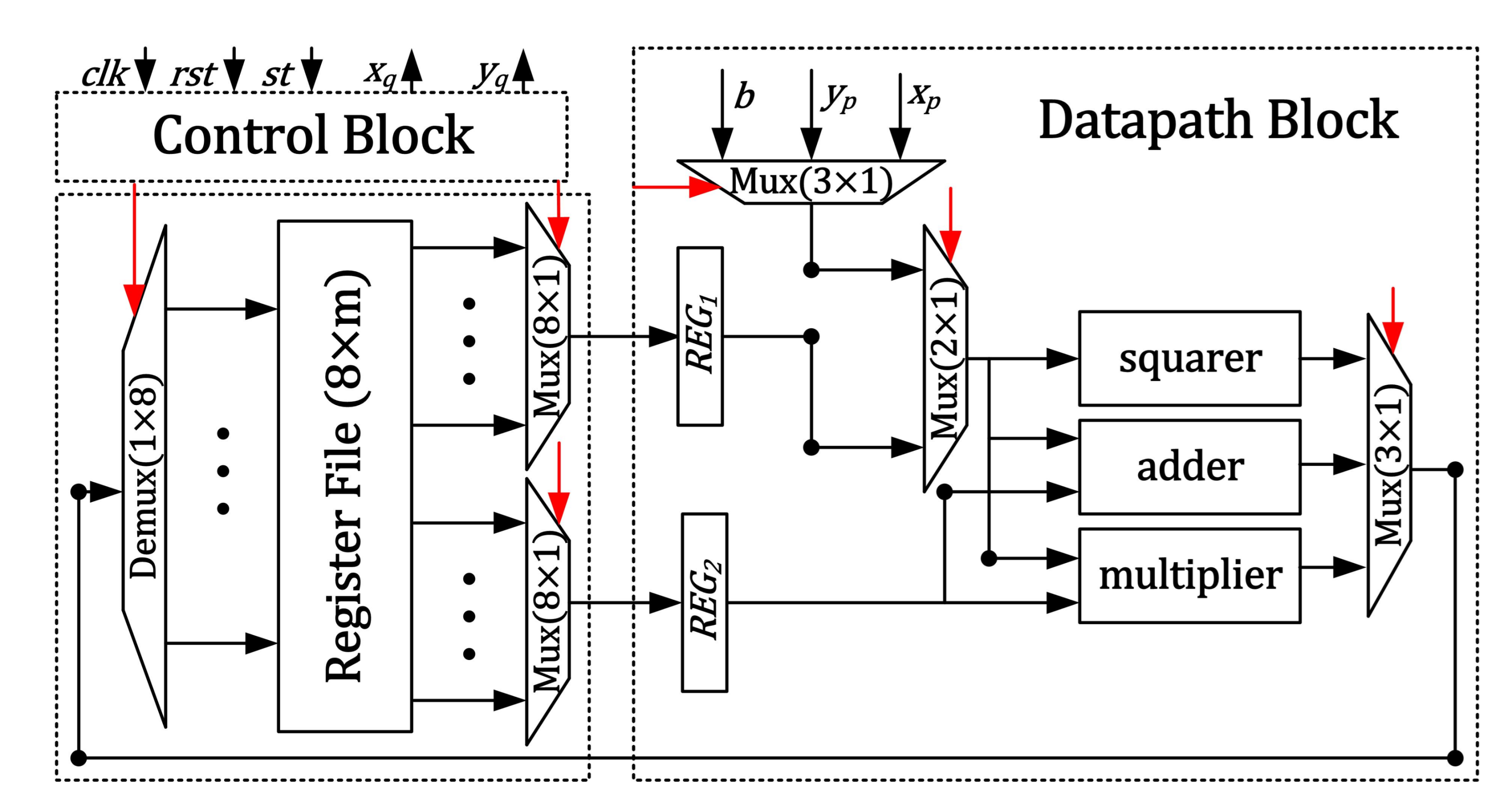
3. Proposed PM Architecture

The proposed PM architecture is shown in Figure 1. It contains three blocks, i.e., (i) a register file, (ii) a control block, and (iii) a data path block. The lines in red determine the control signals generated by the control block. The c l k , r s t , and s t (start) signals are input to the proposed PM architecture. The coordinates of the final point Q are outputs. The scalar multiplier (or the secret key k, given in Algorithm 1) is also considered an input from outside the architecture (not shown in Figure 1). The implementation details of the aforementioned blocks (register file, data path, and control unit) are provided as follows:

3.1. Register File

The proposed architecture aggregates an 8 × m size register file, where m determines the length of each register. This block is responsible for maintaining the intermediate and the final results during/after the execution of a sequence of instructions of Algorithm 1. It contains two multiplexers ( 8 × 1 ) to read the data from the register file for the data path block. Furthermore, a 1 × 8 demultiplexer is used to update the contents of each particular register address.

3.2. Data Path Block

It consists of (i) two pipeline registers, (ii) three routing multiplexers, (iii) an adder, (iv) a squarer, and (v) a multiplier, as shown in Figure 1.

3.2.1. Pipelined Registers and Proposed Scheduling of PA and PD Operations

To shorten the critical path and to increase the clock frequency, we incorporated two pipelined registers (i.e., R E G 1 and R E G 2 ), as shown in Figure 1. The input to each pipeline register is an operand from the register file. The output of R E G 1 is connected to a multiplexer. On the other hand, the output of R E G 2 is directly connected to both adder and multiplier units. It is important to note that the inclusion of two pipelined registers results in the r e a d operation in one clock cycle but in the e x e c u t e and w r i t e b a c k operations in n clock cycles. Here, n determines the execution cost (in terms of clock cycles) of the adder, squarer, and multiplier units. The required clock cycles for the execution of these operations (addition, squaring, and multiplication) are discussed later in this paper. Therefore, to manage with the pipelining, the proposed scheduling of PA (a function, i.e., P A D D ( X 1 , Z 1 ) , from Algorithm 1) and PD (a function, i.e., P D B L ( X 2 , Z 2 ) , from Algorithm 1) operations are shown in Figure 2.
In Figure 2, OP determines the corresponding PA and PD operations. Moreover, INST# presents the total instructions (IN1 to IN14). The original PA and PD instructions in Figure 2 show the number of operations involved in P A D D ( X 1 , Z 1 ) and P D B L ( X 2 , Z 2 ) functions (these functions are briefly described in Section 2). The data dependency (also called as hazard) shows that the next instruction cannot be read (or can be termed instruction fetch) until the result of the previous instruction is written back. For example, IN3 cannot be read as it depends on the result from IN2 (depends on X 1 ). Therefore, we read IN11 instead of IN3 (shown in Figure 2). After completing the execution of IN2 (means after the writeback operation), IN3 is scheduled. We use the same strategy to schedule all fourteen (IN1 to IN14) instructions of P A D D (seven—IN1 to IN7—for PA) and P D B L (seven—IN8 to IN14—for PD) functions for the PM computation.

3.2.2. Routing Multiplexers

The data path includes three routing multiplexers, i.e., two M u x ( 3 × 1 ) and one M u x ( 2 × 1 ) . The first M u x ( 3 × 1 ) is responsible for selectiing an ECC parameter (i.e., x p , y p , and b) required during the implementation of PM operation using Algorithm 1. For our implementations, we selected standardized ECC parameters by the National Institute of Standards and Technology (NIST) [28]. The M u x ( 2 × 1 ) drives the output of M u x ( 3 × 1 ) and an operand from the register file (operand after the R E G 1 ) to arithmetic operators (adder, squarer, and multiplier) for execution. The second M u x ( 3 × 1 ) is responsible for selecting an output from the adder, squarer, and multiplier units for the register file (i.e., to perform write back).

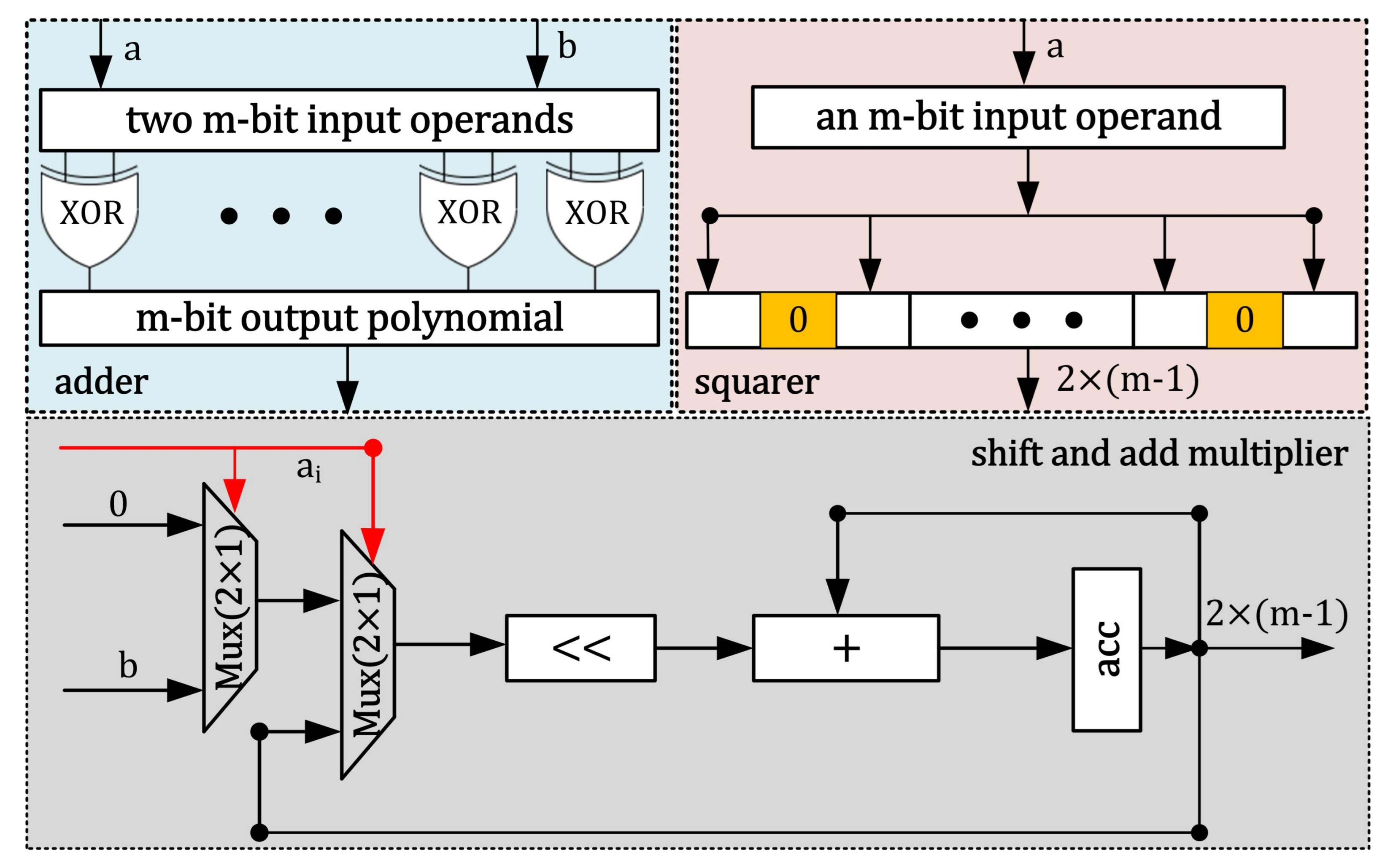
3.2.3. Adder, Squarer, and Multiplier

To implement the PM operation of ECC, the required arithmetic operators are adder, squarer, multiplier, and inversion (not highlighted in Figure 1). The design of the adder, squarer, and multiplier operators are given in Figure 3. Moreover, the implementation attributes of these arithmetic operators are provided in the text that follows:
Adder and Squarer: In G F ( 2 m ) , the computational cost to implement adder and squarer circuits is one clock cycle. Simply, the adder unit is implemented using an array of bitwise Exclusive(OR) gates, as shown in Figure 3. It takes a pair of polynomials (a and b) as input. Moreover, it provides an m bit polynomial as output (shown as c). The squarer architecture is designed by inserting a 0-bit after each input data bit. It is highlighted in orange in Figure 3. It takes the polynomial with a size of m bits. The output is a 2 × m 1 bit polynomial (shown as c).
Multiplier: The performance of an ECC-based crypto processor depends on the efficiency of the used multiplier. In this context, there exist four possibilities: bit-serial, digit-serial, bit-parallel, and digit-parallel to compute polynomial multiplication. For a pair of m bit polynomial multiplications, m clock cycles are needed in the bit-serial multiplication method. Similarly, the computational cost in bit-parallel and digit-parallel multipliers is one clock cycle. Furthermore, x y clock cycles are required for the digit-serial method, where x determines the operand length and y is the digit size. Due to different computational costs, each multiplication possibility has its own pros and cons. For example, the bit-serial multipliers are more beneficial when lower hardware resources and power consumption are required (i.e., RFID- and WSN-related applications). The bit-parallel and digit-parallel multiplier approaches achieve high performances. The digit-serial multipliers are generally preferred for both reduced area and lower computation time applications. Based on this observation, a bit-serial multiplier method (i.e., simple shift and add, as presented in Figure 1) is employed in this work to perform two m bit polynomial multiplications.
A simple shift and add multiplication is identical to the schoolbook multiplication. In other words, this method adds the multiplicand a (first input polynomial) to itself b times, where b is the multiplier (second input polynomial). Therefore, the proposed shift and add multiplier architecture (shown in Figure 1) consists of two 2 × 1 multiplexers; one m bit shift register and adder; and an m bit accumulator register, where m determines the length of multiplicand and multiplier (i.e., a and b). The input to the first 2 × 1 multiplexer is an m bit array of 0’s and a multiplicand b, as shown in Figure 1. The second 2 × 1 multiplexer is used to select an appropriate operand either before of after shifting for the multiplication computation. To perform polynomial multiplication, each clock cycle is responsible for inspecting a multiplicand ( a i ) bit that acts as a select line or control signal to both of the multiplexers. Based on the inspected multiplicand ( a i ) bit value, the corresponding operations (shifting, addition, and accumulation) over the multiplier (i.e., b) are performed. After m clock cycles, a 2 × m 1 bit polynomial is generated as the output.
Reduction. As shown in Figure 1, the output after polynomial squaring and multiplication is a 2 × m 1 bit. Thus, a polynomial reduction is needed to transform 2 × m 1 bit(s) to m bit. Consequently, we employed a NIST-recommended polynomial reduction algorithm (see Algorithm 2.41 of [29]).
Inversion: The PAC step of Algorithm 1 requires two polynomial inversion computations. Therefore, multiple inversion methods can be considered. However, the Itoh–Tsujii inversion algorithm is more frequently utilized as it requires only the multiplications and square operations for the computation [14,18,19,21,22,24,27]. Based on this consideration, we used similar hardware resources of our employed multiplier and squarer architectures to perform the required inversion operations to implement Algorithm 1.
Over G F ( 2 163 ) , the Itoh–Tsujii inversion algorithm requires nine polynomial multiplications and m 1 squares [30]. As described earlier, the employed polynomial multiplier architecture takes m clock cycles to operate one polynomial multiplication. Therefore, nine multiplications require 9 × m clock cycles. For polynomial squaring, m 1 clock cycles are required. Using architectures of Figure 3, the total computational cost (in terms of clock cycles) to implement the Itoh–Tsujii inversion algorithm is ( 9 × m ) + ( m 1 ) .

3.3. Control Block

A controller is designed (FSM based) for the generation of required control signals. To implement the Montgomery algorithm (Algorithm 1), the designed FSM constitutes a total of 108 states. The details are given as follows:
  • Idle state: It represents the start of overall operation. Consequently, State 0 is used for this purpose.
  • States from affine to projective conversions: Based on the start (i.e., s t ) signal, the FSM switches from the idle state to the next state (i.e., state 1). Subsequently, the control signals for projective to affine conversions are generated from state 1 to state 6.
  • PM states: As shown in Algorithm 1, the PM step consists of 14 instructions (6 are for multiplications, 3 are for additions, and 5 are for squares). Out of these 14 instructions, 7 are for PA while the remaining 7 are for PD computations. To implement these 14 instructions, FSM requires 17 states (state 7 to state 23). Moreover, each state from 7 to 23 is responsible for checking the inspected key bit, i.e., k i . Once the value for k i becomes 1, the i f part from Algorithm 1 is implemented. Otherwise, the e l s e part is implemented. These states (7 to 23) are repeated until the condition for the l o o p statement of Algorithm 1 becomes true. Once the loop condition becomes true, the next state is state 24.
  • States from projective to affine conversions: The PAC step requires two inversion operations, as depicted in Algorithm 1. Therefore, each inversion is computed during states 24 to 69. The remaining states from 70 to 108 are responsible for implementing additional instructions of the PAC step.
For the proposed PM architecture, Equation (2) is used to calculate the total clock cycles. The APC step of Algorithm 1 needs six clock cycles. The PMPC step takes ( m 1 ) ( 6 × m ) + 8 clock cycles. The 6 × m clock cycles are needed to execute six polynomial multiplication ( m u l t ) instructions. The additional eight clock cycles are required for polynomial addition and squaring ( a d d and s q r ) instructions. The m 1 determines the repetition of a loop statement of the PMPC step. Finally, the PAC step demands 2 × i n v e r s i o n operations. Clock cycles to compute one inversion is ( 9 × m ) + m 1 . In addition to inversion clock cycles, 1306 cycles are required to complete the execution of the remaining operations of PAC step (it contains eight multiplications, five additions, and five squares). Consequently, the proposed PM architecture over G F ( 2 m ) with m = 163 requires 162,673 clock cycles.
T o t a l c y c l e s = 6 APC step of Algorithm 1 + m 1 6 × m f o r m u l t + 8 f o r a d d & s q r PMPC step of Algorithm 1 + 2 × i n v e r s i o n + 1306 PAC step of Algorithm 1

4. Results and Comparisons

The implementation results for the proposed PM architecture are provided in Section 4.1. Subsequently, a comprehensive discussion with respect to existing PM architectures is presented in Section 4.2. Finally, the possible side channel attack (SCA) leakages and countermeasures for our design are shown in Section 4.3.

4.1. Implementation Results

The proposed PM architecture over G F ( 2 163 ) is designed in Verilog using the Vivado design tool. The functional verification is performed with the associated algorithmic model (written in C language). We selected different Xilinx FPGA devices, i.e., Virtex-4 (a 90 nm process technology), Virtex-5 (a 65 nm process technology), Virtex-6 (a 40 nm process technology), Virtex-7 (a 28 nm process technology), Spartan-7 (a 28 nm process technology), Artix-7 (a 28 nm process technology), and Kintex-7 (a 28 nm process technology), for the performance evaluation of our design. It is important to note that the architectures of our selected devices contain four-input Lookup Tables (LUTs) for Virtex-4 and six-input LUTs for the remaining selected devices. Although the implementations on Virtex-4 are not recommended by vendors for use in recent designs, it is still available to cope with the existing implementations. We believe that the use of different process technologies from 65 nm to 28 nm (as we selected for our synthesis in this work) is a good alternative to evaluating the performance of the design.
The experimental outcomes after synthesis on several Xilinx FPGA devices, i.e., Virtex-4 (xc4vfx140), Virtex-5 (xc5vfx130t), Virtex-6 (xc6vlx550t), Virtex-7 (xc7vx690tffg1930-2), Spartan-7 (xc7s100fgga676-2), Artix-7 (xc7a200tsbv484-2), and Kintex-7 (xc7k480tffv1156-2), are given in Table 1. The reason to choose 7-series FPGA devices (Virtex, Spartan, Artix and Kintex) is to make a real tradeoff between area, power, and performance (throughput) parameters. The first column in Table 1 presents the implementation device. The area information is given in columns two, three, and four. Similarly, columns five and six present the information related to computation time. This information is provided in the form of clock frequency and latency. The last column presents the throughput of our proposed PM architecture. The reported values of area and frequency are obtained with the help of the Vivado tool. The required clock cycles are computed with the help of Equation (2) (given in Section 3.3). Similarly, latency is the computation time needed to execute one point multiplication operation. Furthermore, the ratio of one over latency determines the throughput. Finally, the latency and throughput are calculated using Equation (3) and Equation (4), respectively.
L a t e n c y ( i n μ s ) = T o t a l C l o c k C y c l e s C l o c k F r e q u e n c y ( i n MHz )
T h r o u g h p u t = 1 L a t e n c y ( i n μ s ) = 10 6 L a t e n c y ( i n s )
Comparison with Xilinx Virtex (4, 5, 6, and 7) devices. The results after synthesis over G F ( 2 163 ) show that the area values are decreased when moving from 90 nm (Virtex-4) to a newer 28 nm (Virtex-7) process technology. Similarly, on the Virtex-4, Virtex-5, Virtex-6, and Virtex-7 devices, the proposed architecture achieves 236, 321, 351, and 391 MHz clock frequencies. On the same FPGA devices, the computation times for a single point multiplication operation are 690, 507, 463, and 416 μ s, respectively. Moreover, the proposed architecture over G F ( 2 163 ) provides 1449.2, 1972.3, 2159.8, and 2403.8 throughput values, respectively. When concerning the power consumption of our proposed design on variants of Virtex FPGA devices, it consumes 87 μ W (on 90 nm), 79 μ W (on 65 nm), 76 μ W (on 40 nm), and 71 μ W (on 28 nm). As expected, the highest power is achieved on Virtex-4 as the architecture of the process technology contains four-input LUTs compared with other Virtex devices (Virtex-5, Virtex-6, and Virtex-7), where a six-input LUT architecture is adopted for logic mapping.
Comparison with 7-series FPGA (Virtex-7, Spartan-7, Artix-7, and Kintex-7) devices. According to [31], the architectures of the Spartan-7, Artix-7, Kintex-7, and Virtex-7 devices are optimized for low cost, low power, best price-performance, and the highest system performance, respectively. As shown in Table 1, the low area values—in terms of Slices (433), LUTs (1391), and FFs (1059)—are achieved for Spartan-7 compared with the Artix-7, Kintex-7, and Virtex-7 devices. Comparatively, the higher clock frequency (391 MHz) and throughput (2403.8) values are achieved on Virtex-7 FPGA as the architecture of this device is optimized to achieve the highest system performance. The required computation times for one-point multiplication operations are 416 μ s (on Virtex-7), 518 μ s (on Spartan-7), 501 μ s (on Artix-7), and 448 μ s (on Kintex-7). The lower power of 56 μ W is achieved on the Artix-7 device, while on the other 7-series devices, the power consumptions are 71 μ W (on Virtex-7), 67 μ W (on Spartan-7), and 61 μ W (on Kintex-7).
As shown in Figure 1, our proposed PM architecture consists of a (i) register file, (ii) a datapath block, and (iii) a control block. On different FPGA devices (Virtex-4, Virtex-5, Virtex-6, Virtex-7, Spartan-7, Artix-7, and Kintex-7), the hardware utilization in terms of FPGA Slices of the register file, control and datapath blocks are ± 23%, ± 11%, and ± 66%, respectively. The datapath mostly covers the hardware resources as it contains one 2 × 1 multiplexer, two 3 × 1 multiplexers, two 163-bit pipeline registers, an adder, a squarer, and a multiplier. Moreover, we used two reduction units (not presented in Figure 1) connected after each squarer (first reduction unit) and a multiplier block (second reduction unit). The control block utilizes the lower resources as it contains only the logic to drive incorporated register file and datapath blocks.
Despite the individual evaluations of essential design parameters, i.e., area (slices, LUTs, and FFs) and throughput, we defined another performance index (PI) in Equation (5) to capture the characteristics in terms of throughput and area at the same time. The calculated values on different FPGA devices for the defined PI are shown in Figure 4.
P I = T h r o u g h p u t A r e a ( F P G A s l i c e s )
It is important to note that the higher the throughput over area ratio values are, the higher the performance of the architecture. Therefore, Figure 4 reveals that the proposed architecture results in a higher ratio of throughput over area (4.89) on Xilinx Virtex-7 FPGA. On the Virtex-4, Virtex-5, Virtex-6, Spartan-7, Artix-7, and Kintex-7 devices, the computed ratios of throughput over area are 0.77, 3.89, 4.31, 4.45, 4.25, and 4.73, respectively. There is always a tradeoff between area and throughput parameters.

4.2. Comparison with Existing PM Solutions

Even if a variety of PM architectures have been recently published in the literature [14,15,17,18,19,20,21,22,24,25,26], a comparison with all of these can be a little unfair due to the use of different PM algorithms, implementation fields (such as G F ( P ) ), and platforms. Therefore, a comparison with the most relevant (existing) PM acceleration solutions is given in Table 2. Column one provides the reference number. Different implementation models of ECC and the applied algorithms for the execution of PM are shown in column two. Column three provides the implementation device. The used FPGA slices are given in column four. Finally, columns five and six provide the clock frequency (MHz) and latency ( μ s). Moreover, we have used a representation ‘–’ in Table 2, whenever the essential data were not provided.
Comparison with recent high-speed implementations [14,15,17]. Compared wiht the PM architecture, implemented on Virtex-5 FPGA in [15], the proposed design utilizes 7.23 (ratio of 3670 to 507) times lower hardware resources in terms of slices. Furthermore, our pipelined architecture achieves 1.09 (ratio of 321 over 292) times higher clock frequency. When considering the latency for comparison, the proposed architecture requires 202.8 (ratio of 507 over 2.5) times higher computation time. The reason for this higher computation time is the use of a pipelined bit-parallel modular multiplier accumulator in [15] while we employed a bit-serial schoolbook multiplier. On a Virtex-7 device, our design utilizes 3.24 (ratio of 1593 to 491) times lower slices compared with the work in [14]. Furthermore, our pipelined design achieves 1.33 (ratio of 391 over 293) times higher clock frequency. Similar to [15], the proposed architecture requires 113.04 (ratio of 416 over 3.68) times higher computation time. The time to compute one PM operation in [14] is reduced by using two modular multipliers and squares. In our case, we used only one modular multiplier and a square unit. Compared with the Kintex-7 implementation of [17], our proposed design utilizes 4.78 (ratio of 2253 to 471) times lower FPGA slices. Moreover, our design achieves 1.18 (ratio of 363 over 306) times higher clock frequency. The comparison to the computation time is not possible as the relevant information is not provided.
Comparison with area-optimized implementations [18,19,20,21] The solutions described in [19,20] are implemented on a Virtex-5 device while Virtex-7 implementations are provided in [18,21]. With respect to the work in [19], our design utilizes 1.07 (ratio of 507 to 473) times higher area values. The reason is the utilization of an 8-bit I/O interface to achieve the flexibility in [19]. In our design, we used an m-bit interface that infers higher slices. Similar to the area (FPGA slices), the architecture of [19] provides 1.11 (ratio of 359 over 321) times better clock frequency. The BEC model of ECC is preferred for the PM computation in [20]. The proposed architecture utilizes 6.15 (ratio of 3122 to 507) times lower area values with respect to the work in [20]. Moreover, the proposed architecture achieves a 1.11 (ratio of 321 over 288) times higher clock frequency. When considering the latency for the comparison, the proposed architecture takes 20.67 (ratio of 507 over 24.52) times higher computation time. On Virtex-7 FPGA, the proposed design utilizes 7.44 (ratio of 3657 to 491) and 3.11 (ratio of 1529 to 491) times lower slices compared with the architecture reported in [18,21] respectively. The frequency comparison with [18] is not feasible due to the lack of available information. It has been observed that our design is 1.02 (ratio of 391 over 383) times faster compared with [21]. With respect to the work in to [18,21], our design requires 16.44 (ratio of 416 over 25.3) and 41.97 (ratio of 416 over 9.91) times higher computation time.
Comparison with throughput and area optimized architectures [22,24]. To accelerate the point multiplication, a pipelining scheme with two stages is given in [22]. Moreover, the rescheduling of point addition and point doubling operations is provided. The work in this article also employed pipelined registers to shorten the critical path. On Xilinx Virtex-7 FPGA, our pipelined architecture utilizes only 491 slices that are 4.49 times lower than the solution in [22]. The comparison in terms of clock frequency reveals that the proposed design is 1.05 times faster compared with the solution in [22]. The lower clock cycles utilization decreases the computation time (latency). However, the architecture of [22] takes 38.76 (ratio of 416 over 10.73) times lower computation time (latency) compared with our architecture. A segmented pipelined multiplier design is employed in [24] to minimize area with an optimal clock frequency. With a similar clock frequency (391 in this work and 397 in [24]), the employment of a bit-serial multiplier in our design results in an area reduction. In other words, the use of a schoolbook multiplier results in a 3 (ratio of 1476 over 491) times decrease in FPGA slices compared with the work in [24]. Furthermore, the proposed architecture requires a 39.58 (ratio of 416 over 10.73) times higher computation time (latency) compared with [24].

4.3. Possible Leakages and Countermeasures

Similar to [25], each iteration of the selected PM algorithm (described in Section 2) requires one PA and PD operation per ladder step independent of the inspected key bit value. The execution of other operations (conversion from affine to projective coordinates and vice versa) are performed in a constant number of clock cycles. Based on these observations (i.e., constant time and secret independent execution of PA and PD operations), we assume that the proposed design is inherently resistant to timing and SPA attacks. On the other hand, a 163-bit scalar multiplier (k) as input from an external user is kept in a register (before starting the PM computation). Moreover, after the PM computation, the generated coordinates ( x q and y q ) of final point Q are stored in our employed register file (we refer readers to Figure 1). Similarly, the generated final coordinates are stored in pipeline registers ( R E G 1 and R E G 2 ). It is noteworthy that the pipeline registers are connected to the output ports, i.e., x q and y q , of the proposed PM design (not shown in Figure 1). Therefore, the storage of the scalar multiplier and the coordinates of the final point in storage elements may open doors for the attacker to steal secrets using a SPA attack. Connecting our design outputs (shown with x q and y q in Figure 1) directly to the outputs from the register file could provide resistance to possible SPA attacks.

5. Conclusions

This paper has provided a PM architecture of ECC over G F ( 2 163 ) with the consideration of latency and hardware resources (FPGA slices) concurrently. The FPGA slices are reduced using a schoolbook multiplier. The latency of the architecture is considered for optimizations using pipelining. The use of pipelining reduces the critical path of the architecture, which ultimately improves the clock frequency. With the aforementioned optimization strategies, the synthesis is performed on Virtex-4, Virtex-5, Virtex-6, Virtex-7, Spartan-7, Artix-7, and Kintex-7. Consequently, the used FPGA slices over G F ( 2 163 ) are 1880, 507, 501, 491, 433, 469, and 471. Similarly, the calculated ratios of throughput over slices values are 0.77, 3.89, 4.31, 4.89, 4.45, 4.25, and 4.73. It has been observed that the use of a schoolbook multiplier consumes lower hardware resources (less than 400 slices) on modern FPGA devices such as Virtex-7, Spartan-7, Artix-7, and Kintex-7. However, it needs relatively more computation time (latency) compared with existing accelerators for PM operation. In other words, there is always a tradeoff between performance (latency) and area. To summarize, the achieved results in this article suggest the applicability of our work in area-efficient competitive cryptographic designs.

Author Contributions

Conceptualization, M.R., M.M.H., S.Z.K. and A.S.; data extraction, A.R.A., M.M.H. and A.S.; results compilation, A.R.A., M.M.H., M.R. and S.Z.K.; validation, S.Z.K. and M.R.; writing—original draft preparation, M.R., A.S. and S.Z.K.; critical review, A.R.A., M.R. and M.M.H.; draft optimization, A.A.; supervision, M.M.H. and M.R.; funding acquisition, M.M.H. All authors have read and agreed to the published version of the manuscript.

Funding

The author Mohammad Mazyad Hazzazi extends his gratitude to the Deanship of Scientific Research at King Khalid University for funding this work through a research group program under grant number R.G.P. 2/150/42.

Conflicts of Interest

The authors declare no conflict of interest.

References

  1. Verri Lucca, A.; Mariano Sborz, G.A.; Leithardt, V.R.Q.; Beko, M.; Albenes Zeferino, C.; Parreira, W.D. A Review of Techniques for Implementing Elliptic Curve Point Multiplication on Hardware. J. Sens. Actuator Netw. 2021, 10, 3. [Google Scholar] [CrossRef]
  2. Rashid, M.; Imran, M.; Jafri, A.R.; Al-Somani, T.F. Flexible Architectures for Cryptographic Algorithms — A Systematic Literature Review. J. Circuits Syst. Comput. 2019, 28, 1930003. [Google Scholar] [CrossRef]
  3. Mallouli, F.; Hellal, A.; Sharief Saeed, N.; Abdulraheem Alzahrani, F. A Survey on Cryptography: Comparative Study between RSA vs. ECC Algorithms, and RSA vs El-Gamal Algorithms. In Proceedings of the 2019 6th IEEE International Conference on Cyber Security and Cloud Computing (CSCloud)/2019 5th IEEE International Conference on Edge Computing and Scalable Cloud (EdgeCom), Paris, France, 21–23 June 2019; pp. 173–176. [Google Scholar] [CrossRef]
  4. Yadav, A.K. Significance of Elliptic Curve Cryptography in Blockchain IoT with Comparative Analysis of RSA Algorithm. In Proceedings of the 2021 International Conference on Computing, Communication, and Intelligent Systems (ICCCIS), Greater Noida, India, 19–20 February 2021; pp. 256–262. [Google Scholar] [CrossRef]
  5. Suárez-Albela, M.; Fernández-Caramés, T.M.; Fraga-Lamas, P.; Castedo, L. A Practical Performance Comparison of ECC and RSA for Resource-Constrained IoT Devices. In Proceedings of the 2018 Global Internet of Things Summit (GIoTS), Bilbao, Spain, 4–7 June 2018; pp. 1–6. [Google Scholar] [CrossRef]
  6. Käsper, E. Fast Elliptic Curve Cryptography in OpenSSL. In Financial Cryptography and Data Security; Danezis, G., Dietrich, S., Sako, K., Eds.; Springer: Berlin/Heidelberg, Germany, 2012; pp. 27–39. [Google Scholar] [CrossRef] [Green Version]
  7. Kikwai, B.K. Elliptic Curve Digital Signatures and Their Application in the Bitcoin Crypto-currency Transactions. Int. J. Sci. Res. Publ. 2017. Available online: http://www.ijsrp.org/research-paper-1117.php?rp=P716921 (accessed on 26 August 2021).
  8. Khoirom, M.S.; Laiphrakpam, D.S.; Themrichon, T. Cryptanalysis of multimedia encryption using elliptic curve cryptography. Optik 2018, 168, 370–375. [Google Scholar] [CrossRef]
  9. Li, C.; Zhang, Y.; Xie, E.Y. When an attacker meets a cipher-image in 2018: A Year in Review. arXiv 2019, arXiv:cs.CR/1903.11764. [Google Scholar] [CrossRef] [Green Version]
  10. Zhang, Y.; Li, B.; Liu, B.; Hu, Y.; Zheng, H. A Privacy-Aware PUFs-Based Multi-Server Authentication Protocol in Cloud-Edge IoT Systems Using Blockchain. IEEE Internet Things J. 2021, 8, 13958–13974. [Google Scholar] [CrossRef]
  11. Liu, Z.; Liu, D.; Zou, X.; Lin, H.; Cheng, J. Design of an Elliptic Curve Cryptography Processor for RFID Tag Chips. Sensors 2014, 14, 17883–17904. [Google Scholar] [CrossRef] [PubMed] [Green Version]
  12. Noori, D.; Shakeri, H.; Niazi, T.M. Scalable, efficient, and secure RFID with elliptic curve cryptosystem for Internet of Things in healthcare environment. Eurasip J. Inf. Secur. 2020, 2020, 13. [Google Scholar] [CrossRef]
  13. Zhan, L.; Yong, X.; Weibin, L.; Yun, Z.; Chao, C.; Ziwen, C. A High-Speed Elliptic Curve Cryptography Processor for Teleoperated Systems Security. Math. Probl. Eng. 2021, 2021, 6633925. [Google Scholar] [CrossRef]
  14. Rashid, M.; Imran, M.; Sajid, A. An Efficient Elliptic-Curve Point Multiplication Architecture for High-Speed Cryptographic Applications. Electronics 2020, 9, 2126. [Google Scholar] [CrossRef]
  15. Li, L.; Li, S. High-Performance Pipelined Architecture of Point Multiplication on Koblitz Curves. IEEE Trans. Circuits Syst. II Express Briefs 2018, 65, 1723–1727. [Google Scholar] [CrossRef]
  16. Awaludin, A.M.; Larasati, H.T.; Kim, H. High-Speed and Unified ECC Processor for Generic Weierstrass Curves over GF(p) on FPGA. Sensors 2021, 21, 1451. [Google Scholar] [CrossRef] [PubMed]
  17. Hossain, M.S.; Saeedi, E.; Kong, Y. High-Performance FPGA Implementation of Elliptic Curve Cryptography Processor over Binary Field GF(2163). In Proceedings of the 2nd International Conference on Information Systems Security and Privacy, Rome, Italy, 19–21 February 2016. [Google Scholar] [CrossRef] [Green Version]
  18. Imran, M.; Rashid, M.; Shafi, I. Lopez Dahab based elliptic crypto processor (ECP) over GF(2163) for low-area applications on FPGA. In Proceedings of the 2018 International Conference on Engineering and Emerging Technologies (ICEET), Lahore, Pakistan, 22–23 February 2018; pp. 1–6. [Google Scholar] [CrossRef]
  19. Khan, Z.U.A.; Benaissa, M. Low area ECC implementation on FPGA. In Proceedings of the 2013 IEEE 20th International Conference on Electronics, Circuits, and Systems (ICECS), Abu Dhabi, United Arab Emirates, 8–11 December 2013; pp. 581–584. [Google Scholar] [CrossRef]
  20. Rashidi, B. Low-Cost and Fast Hardware Implementations of Point Multiplication on Binary Edwards Curves. In Proceedings of the Electrical Engineering (ICEE), Iranian Conference on, Mashhad, Iran, 8–10 May 2018; pp. 17–22. [Google Scholar] [CrossRef]
  21. Imran, M.; Pagliarini, S.; Rashid, M. An Area Aware Accelerator for Elliptic Curve Point Multiplication. In Proceedings of the 2020 27th IEEE International Conference on Electronics, Circuits and Systems (ICECS), Glasgow, UK, 23–25 November 2020; pp. 1–4. [Google Scholar] [CrossRef]
  22. Imran, M.; Rashid, M.; Jafri, A.R.; Kashif, M. Throughput/area optimised pipelined architecture for elliptic curve crypto processor. Iet Comput. Digit. Tech. 2019, 13, 361–368. [Google Scholar] [CrossRef] [Green Version]
  23. Islam, M.M.; Hossain, M.S.; Shahjalal, M.; Hasan, M.K.; Jang, Y.M. Area-Time Efficient Hardware Implementation of Modular Multiplication for Elliptic Curve Cryptography. IEEE Access 2020, 8, 73898–73906. [Google Scholar] [CrossRef]
  24. Khan, Z.U.A.; Benaissa, M. Throughput/Area-efficient ECC Processor Using Montgomery Point Multiplication on FPGA. IEEE Trans. Circuits Syst. II Express Briefs 2015, 62, 1078–1082. [Google Scholar] [CrossRef]
  25. Bisheh-Niasar, M.; Azarderakhsh, R.; Mozaffari-Kermani, M. Cryptographic Accelerators for Digital Signature Based on Ed25519. IEEE Trans. Very Large Scale Integr. (VLSI) Syst. 2021, 29, 1297–1305. [Google Scholar] [CrossRef]
  26. Bisheh Niasar, M.; Azarderakhsh, R.; Kermani, M.M. Efficient Hardware Implementations for Elliptic Curve Cryptography over Curve448. In Progress in Cryptology—INDOCRYPT 2020; Bhargavan, K., Oswald, E., Prabhakaran, M., Eds.; Springer International Publishing: Cham, Switzerland, 2020; pp. 228–247. [Google Scholar]
  27. Sajid, A.; Rashid, M.; Imran, M.; Jafri, A.R. A Low-Complexity Edward-Curve Point Multiplication Architecture. Electronics 2021, 10, 1080. [Google Scholar] [CrossRef]
  28. NIST. Recommended Elliptic Curves for Federal Government Use (1999). Available online: https://csrc.nist.gov/csrc/media/publications/fips/186/2/archive/2000-01-27/documents/fips186-2.pdf (accessed on 19 September 2021).
  29. Hankerson, D.; Menezes, A.J.; Vanstone, S. Guide to Elliptic Curve Cryptography. 2004, pp. 1–311. Available online: https://0-link-springer-com.brum.beds.ac.uk/book/10.1007/b97644 (accessed on 13 August 2021).
  30. Zode, P.; Deshmukh, R.B.; Samad, A. Fast Architecture of Modular Inversion Using Itoh-Tsujii Algorithm. In VLSI Design and Test; Kaushik, B.K., Dasgupta, S., Singh, V., Eds.; Springer: Singapore, 2017; pp. 48–55. Available online: https://www.springerprofessional.de/fast-architecture-of-modular-inversion-using-itoh-tsujii-algorit/15326436 (accessed on 3 September 2021).
  31. XILINX. 7 Series FPGAs Data Sheet: Overview. Available online: https://www.mouser.ee/pdfDocs/Virtex-7-ds180_7Series_Overview.pdf (accessed on 17 October 2021).
Figure 1. Proposed PM architecture.
Electronics 10 02698 g001
Figure 2. Proposed scheduling of PADD and PDBL functions (from Algorithm 1) for the computation of PM operation in ECC.
Electronics 10 02698 g002
Figure 3. Architectures for polynomial adder, squarer, and Shift and Add multiplier.
Electronics 10 02698 g003
Figure 4. Throughput over area results (we used FPGA slices as areas for the calculation).
Electronics 10 02698 g004
Table 1. Synthesis results over G F ( 2 163 ) on different FPGA devices.
DeviceArea UtilizationTiming InformationThroughputTotal Power
SlicesLUTsFFsFreq. ( in MHz)Latency (in μ s)
Virtex-41880564011642366901449.287
Virtex-5507152111563215071972.379
Virtex-6501150611493514632159.876
Virtex-7491147311413914162403.871
Spartan-7433139110593145181930.567
Artix-7469142110663255011996.056
Kintex-7471143310693634482232.161
The total power is the sum of static and dynamic powers. The required clock cycles for one PM computation is 162673 (see Section 3.3 for details).
Table 2. Area and timing comparison with various existing architectures over G F ( 2 163 ) .
Ref #.ECC Models/PM AlgorithmPlatformArea (FPGA Slices)Timing Information
Freq. (in MHz)Latency (in μ s)
High-speed architectures
[15]Weierstrass/Right to LeftVirtex-536702922.50
[14]Weierstrass/MontgomeryVirtex-715932933.68
[17]Weierstrass/–Kintex-72253306
Low-area implementations
[19]Weierstrass/MontgomeryVirtex-5473359110
[20]BEC/MontgomeryVirtex-5312228824.52
[18]Weierstrass/MontgomeryVirtex-7365725.3
[21]Weierstrass/MontgomeryVirtex-715293839.91
Throughput and area improved designs
[22]Weierstrass/MontgomeryVirtex-7220736910.73
[24]Weierstrass/MontgomeryVirtex-7147639710.51
Virtex-5507321507
This workWeierstrass/MontgomeryVirtex-7491391416
Kintex-7471363448
BEC: Binary Edward Curves (a special class of Weirstrass model of ECC).
Publisher’s Note: MDPI stays neutral with regard to jurisdictional claims in published maps and institutional affiliations.

