
Design And Implementation of Low Area/Power Elliptic Curve Digital Signature Hardware Core


1
Faculty of Sciences, LR99ES30 EmE Lab, University of Monastir, Monastir 5000, Tunisia
2
Higher Institute of Applied Sciences and Technology, Department of Electronic Engineering, Taffala City,4003 Sousse, Tunisia
*
Author to whom correspondence should be addressed.
Electronics 2017, 6(2), 46; https://0-doi-org.brum.beds.ac.uk/10.3390/electronics6020046
Submission received: 30 December 2016
/
Revised: 2 June 2017
/
Accepted: 7 June 2017
/
Published: 19 June 2017
(This article belongs to the Special Issue Cryptographic Hardware for Embedded Systems)
Abstract
:The Elliptic Curve Digital Signature Algorithm (ECDSA) is the analog to the Digital Signature Algorithm (DSA). Based on the elliptic curve, which uses a small key compared to the others public-key algorithms, ECDSA is the most suitable scheme for environments where processor power and storage are limited. This paper focuses on the hardware implementation of the ECDSA over elliptic curves with the 163-bit key length recommended by the NIST (National Institute of Standards and Technology). It offers two services: signature generation and signature verification. The proposed processor integrates an ECC IP, a Secure Hash Standard 2 IP (SHA-2 Ip) and Random Number Generator IP (RNG IP). Thus, all IPs will be optimized, and different types of RNG will be implemented in order to choose the most appropriate one. A co-simulation was done to verify the ECDSA processor using MATLAB Software. All modules were implemented on a Xilinx Virtex 5 ML 50 FPGA platform; they require respectively 9670 slices, 2530 slices and 18,504 slices. FPGA implementations represent generally the first step for obtaining faster ASIC implementations. Further, the proposed design was also implemented on an ASIC CMOS 45-nm technology; it requires a 0.257 mm area cell achieving a maximum frequency of 532 MHz and consumes 63.444 (mW). Furthermore, in this paper, we analyze the security of our proposed ECDSA processor against the no correctness check for input points and restart attacks.
1. Introduction
Being proposed in 1992, research tended to draw too much attention to the Elliptic Curve Digital Signature Algorithm (ECDSA). Due to its different advantages compared to DSA and Rivest–Shamir–Adleman-system (RSA), which are its small key length and its speed of signature operations, ECDSA was recommended by organizations, such as NIST [1] and Certicom [2]. Computations needed for ECDSA authentication are the generation of a key pair (private key, public key), the computation of a signature and the verification of a signature. Firstly, the production of the key is based on the random or pseudorandom bit sequences. Thus, the first step is to find the appropriate algorithms for producing these bit sequences called the key. There are many algorithms, but the quality of these generated binary sequences should be tested, and their randomness should be checked. Hence, the appropriate algorithm should be deterministic and should generate these keys reliably and quickly. Secondly, ECDSA uses ECC scalar multiplication based on the hardness of solving the Elliptic Curve Discrete Logarithm Problem (ECDLP) and its smaller key size at the same security level compared to other asymmetric cryptosystems. Key size offers a significant gain in terms of speed, power, bandwidth and storage. Point multiplication is the most common operation in ECC, which can be performed by the Montgomery ladder algorithm [3]. Finally, the signature generation and verification are performed using also “SHA-2”. This is a family of hash functions containing the four standardized algorithms SHA-224, SHA-256, SHA-384 and SHA-512, which was developed and standardized by the official NIST standard [4]. By the use of larger digest messages, SHA-2 represents the most resistance to possible attacks, and it can be used with larger blocks of data. Much research was done to implement and to evaluate the ECDSA performances. In 2009, the authors in [5] implemented ECDSA to avoid vehicular accidents by using secure broadcast Vehicle-to-Vehicle (V2V) communications. The authentication mechanism used the ECDSA algorithm with the IEEE1609.2 standard for vehicular ad hoc networks. In 2010, the authors in [6] proposed the implementation of American National Standards Institute (ANSI) called X9.62 ECDSA over prime elliptic curve . In 2012, the authors in [7] implemented ECDSA using ECC curves with a 163-bit key length, key stream generator “W7”, to generate the private key. ECDSA hardware implementation on Xilinx xc6vlx760-2ff1760 requires 0.2 ms, 0.8 ms and 0.4 ms with 7%, 13% and 5% of the device resources on slice LUT for respectively key generation, signature generation and signature verification. In 2016, the authors in [8] studied the side-channel resistance of the implementation of the ECDSA signature scheme in Android’s standard cryptographic library. In this paper, the ECDSA hardware architecture and its performances using FPGA and the ASIC platform will be described. Firstly, the RNG will be studied. Thus, the security analyses of some RNG will be done. Then, they will be implemented in order to choose the appropriate one. Secondly, the implementation of the ECC point multiplication and the SHA-2 function will be presented based on hardware optimizations, which consist of the scheduling and the re-utilization of components. They have a significant impact on the critical path and the area occupancy. Then, a co-simulation of the ECDSA processor design will be done in order to verify its efficiency. Finally, to test the robustness of the proposed ECDSA design, security analyses will be discussed by applying two attacks: the fault injection attack (no correctness check for input points) and the restart attack. The remainder of this paper is organized as follows. Section 2 surveys previous ECDSA works. The methodology and design flow of the ECDSA design will be detailed in Section 3. Section 4 presents the different IPs implementation (ECC over finite fields, a reconfigurable architecture for the hash functions IP, the grain IP). In Section 5, the proposed hardware architecture performing ECDSA will be detailed. Section 6 gives performances evaluation of implementation results, and a comparison with the state-of-the-art will be done. Finally, we will evaluate the security level of the ECDSA processor by applying two security analyses in Section 7. A conclusion of the proposed work will be given in Section 8.
2. Related Works
This section focuses on the previous state-of-the-art ECDSA implementations. In the literature, only a small number of full ECDSA implementations has been reported. To ensure the authentication and verification scheme for the IEEE Wireless Access in Vehicular communication (WAVE), which is based on Vehicular Ad hoc Networks (VANETs), the authors launch in [9] the vehicular message authentication and the prioritized verification for periodic safety messages. They developed the ECDSA mechanism incorporating an Identity-based (ID-based) signature. However, the authors in their work did not mention this and studied the IPs used in the signature process. Moreover, their authentication scheme is insecure since in their modified ECDSA, the random number of ECDSA is replaced with a hashed value for the signature generation. In [10], the authors presented a flexible NFC-tag architecture that provides enhanced security features using symmetric (AES), as well as asymmetric cryptography (ECDSA). For the scalar multiplication, they used the Montgomery algorithm and the projective coordinates. Furthermore, for the hash function, the SHA-1 is used, but is insecure against attacks, and it is much slower compared to SHA-2. The implementation of the design is done in VHDL using 0.35-s CMOS. From the synthesis results, it is clear that their design is slower than the state-of-the-art designs. In 2014, a software optimization of elliptic curve cryptography with 256-bit prime fields was done in [11]. The proposition of the constant-time implementation of the NIST and SECG (Standards for Efficient Cryptography Group) prime curve over accelerate and improve the efficiency the perfect forward secrecy TLS (Transport Layer Security) handshakes, which use the two elliptic curve cryptosystems ECDSA and/or ECDHE (Elliptic Curve Diffie-Hellman Ephemeral). In this paper, the authors are only interested in the optimization of just the public key cryptosystem ECC (i.e., the hash function and the random number generator are not optimized). They performed three optimizations. First, they implement the scalar by G (the Generator) with the windowing method and Booth encoding, using a window of size seven, and avoid MSQR (Montgomery Square) via pre-computation. Second, they speed up point multiplication (for a general point P and also by G) by writing MM (Montgomery Multiplication) and MSQR assembly routines, which are specifically optimized for the MF (Montgomery Friendly modulus) prime p 256. They use the windowing method with Booth encoding, but with a smaller window size of five. Finally, they use the projective coordinates, and the modular inversion is implemented with the little Fermat theorem method. The software patch makes the entire ECDSA sign function constant time, which is resistant to attacks. The software implementation is done with the assembly language. These optimizations accelerate the hall design. In [12], a low-resource implementation of a 160-bit ECDSA signature generation algorithm over prime field curve secp160r1 is presented. The novel hardware architecture of the Keccak hashing algorithm is presented. Moreover, they applied co-Z ECC formulae (add two projective points sharing the same Z-coordinate), a pipelined multiplication unit and RAM macros, and they evaluated fixed-base comb methods to improve the efficiency of ECDSA on passive tags. Furthermore, their design runs with constant runtime and provides basic resistance against common implementation attacks. From the hardware implementation, it requires a total area of 12,448 GEs (or 63,700 m in 130 nm) and can generate a message digest within 140 k cycles. It has a power consumption of 42.42 W at 1 MHz on a low-leakage 130-nm CMOS process technology. However, their design is slower and occupied more area than ours. In the same year, the authors in [13], proposed a design of an elliptic curve cryptography processor as an application for RFID tag chips. The works cited below are vulnerable to attacks. Some techniques can be applied to test and study the design architecture, such as in [14]; the authors studied the hot carrier injection stress effect on a 65-nm low-noise transistor. Furthermore, in [15], the authors examined the temperature and process variability on a p-channel MOSFET voltage multiplier and determined their impact on the voltage multiplier; this method can be applied to the global ECDSA design. In 2017, Wuqiong Pan et al. [16] developed a high-performance signature server called Guess. It implements the ECDSA with a 256-bit key size on a Linux-powered commodity computer, harnessing a desktop Graphics Processing Unit (GPU) as a featured cryptographic accelerator. This server Guess is designed to be resistant to timing attacks. Their contribution is a novel, systematic and inclusive implementation of ECDSA, turning cryptographic theory into productivity on off-the-shelf processors. They optimize the point multiplication (employing Pre-Computing Table (PCT) built offline), point addition (using mixed Jacobian-affine addition) and point doubling (Jacobian system) to accelerate the computation signature generation and signature verification. Besides maximizing computing power, various algorithms are customized and optimized for the platform. Guess readily supports various categories of ECC schemes like digital signature, key agreement and encryption. Guess achieves a throughput equal to Operations Per Second (OPS) for signature generation and OPS for verification. We can note that the authors just optimize the ECC IP, and their implementation results achieve a high throughput, but it consumes high energy. As we can see, every proposed design should be evaluated, and its security should be studied. However, these cryptosystems can be implemented in small devices such as mobile, smart cards and RFID. Bi et al. [17] tried to protect Radio-Frequency (RF) designs by applying a split manufacturing method in RF circuit protection, developing a quantitative security evaluation method to measure the protection level of RF designs under this split manufacturing and demonstration. One of the important field of research is how to protect an Integrated Circuit (IC) from different attacks and finding efficient countermeasures against IC piracy. In this context, Alasad et al. [18] proposed to insert the Multiplexer (MUX) with two cases: firstly, by randomly inserting MUXs equal to half of the output bit number (half MUX insertions), and secondly, by inserting MUXs equal to the number of output bits (full MUX insertions). They adopted Hamming distance as a security evaluation, and they measured the delay, power and area overheads with this proposed technique.
3. ECDSA Processor Methodology and Flow Design
The design flow and needs analyses are the most important tasks in order to obtain a system that verifies the requirements’ specification. In order to find such a design, these instructions have to be followed:
- Select the most suitable algorithms for designing signature IP blocks with respect to the large-scale application’s requirement: a high-security level, a minimum area with maximum throughput and a low consumption.
- Propose RTL (Register Transfer Level) architectural optimizations with the aim of adopting and scaling the signature processor to both the application needs and the platform specifications.
- Propose a hardware verification approach to the proposed signature processor so as to validate and verify RTL implementations. In order to accelerate the verification of the overall architecture, the verification and validation have to apply different co-simulation methods to the used IPs. This can be done thanks to the interfaces between the higher level system environments and the high-performance HDL simulators.
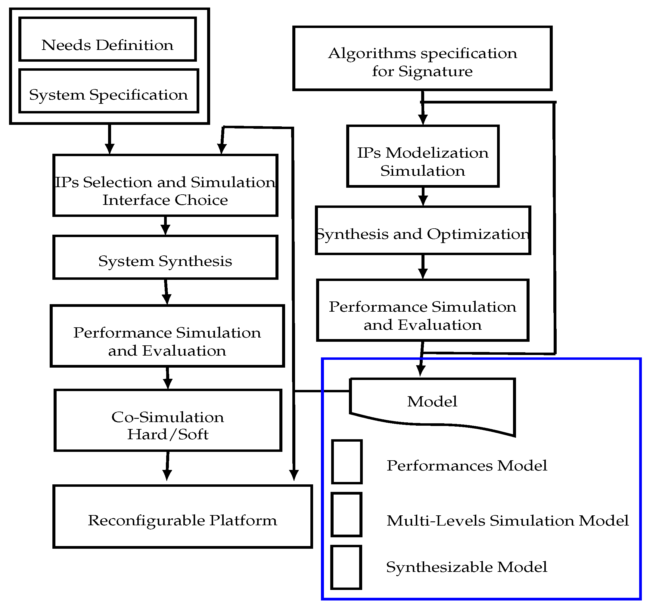
Figure 1 resumes the design flow of the digital signature proposed in this paper. Using the mentioned design flow, to develop and to design a secure digital signature processor, the following strategic points have to be fixed:
- Definition and specification of algorithms for key generation, signature generation and signature verification,
- Design and modeling of different IP and the choice of a standard interface,
- System-level evaluation of security and throughput performances,
- Logic synthesis of different IPs (SHA-2 IP, ECC IP, RNG IP) and integration on a reconfigurable platform,
- Hardware and software co-simulation of the entire signature processor and performance evaluation.
Focusing on the application’s requirements, the different elements needed in the system should be represented and placed into the system requirement analyses process. The main purpose of the needs analyses is the application satisfaction. With respect to the application’s requirements and the chosen platform constraints, the appropriate methods will be fixed to design different needed IPs:
- The most used algorithms for hash are Message Digest algorithm 5 (MD5) and Secure Hash Algorithm (SHA-0, SHA-1 and SHA-2). Thus, MD5, SHA-1 and SHA-0 have the same size of the message, the word and the block. Furthermore, they have the same number of rounds, except that the size of the MD5 digest (128-bit) is smaller than the SHA 0 and SHA-1 ones (160-bit). Collision has been found in MD5, SHA-0 and SHA-1 with a number of attacks [19], which made them unreliable and unsafe, so not adaptable for the actual cryptographic needs. Since their appearance, the SHA-2 family is the most used hash function thanks to the higher security against attacks due to the larger condensed size and speed.
- Due to their flexibility and enhanced ability to manage keys, asymmetric algorithms, such as the Rivest–Shamir–Adleman-system (RSA) and Elliptic Curve Cryptography (ECC), are the most practical cryptosystems. ECC is based on the algebraic structure of elliptic curves over finite fields. It requires smaller key sizes compared to RSA, which allow it to be more suitable for embedded systems that are low-memory and low-power. Indeed, a 256-bit ECC public key provides comparable security to a 3072-bit RSA public key. It is applicable for encryption/decryption, digital signatures, pseudorandom generators, etc. Based on the Elliptic Curve Discrete Logarithm Problem (ECDLP), ECC is very hard to break.
- Key generation is not only needed in symmetric or asymmetric encryption, but also in access codes, passwords, product identification and software authentication. There are several methods for hardware key generation; the best known are the Linear Feed Back Shift Registers (LFSRs), NonLinear Feed Back Shift Registers (NLFSRs), known as grain [20], and the cellular automata, which are an important family of stream cipher generators [21]. The appropriate algorithm in our case is grain-128, because it supports the 128-bit key, and its initial vector is about 96 bits. This encryption is very small and easy to implement in hardware [22]. In addition, it is possible and easy to speed up the hardware design. The grain-128 uses an LFSR to ensure good statistical properties; an NLFSR is used with a non-linear filter to introduce non-linearity. The non-linear filter takes the contribution of the two shift registers.
In order to provide savings on the system’s final cost, area and power consumption, the grain-128, the ECC and the SHA-2 hash function studied earlier will be adopted to design the proposed ECDSA processor. The state-of-the-art works will be the subject of the next section.
4. Proposed Hardware Architecture for ECDSA IPs
In this section, the architectural design of each IP will be discussed in order to implement low-power and low-area ECDSA design. Different optimizations were made to decrease area occupancy and power consumption. Then, optimized IPs are assembled for an efficient ECDSA design. In order to decide how efficient the design is, we calculate the throughput and the efficiency of each IP, such as:
4.1. Secure Hash Standard 2 IP
In order to ensure the data integrity, different cryptographic hash functions can be used. The SHA-2 function offers a higher security, and it is resistant to the collisions. Further, SHA-256 is the most used because it is considered cryptographically safe. In this section, the hardware design and implementation of SHA-2 IP will be presented. Then, the hardware performances will be compared and evaluated.
4.1.1. SHA-2 Architecture Design
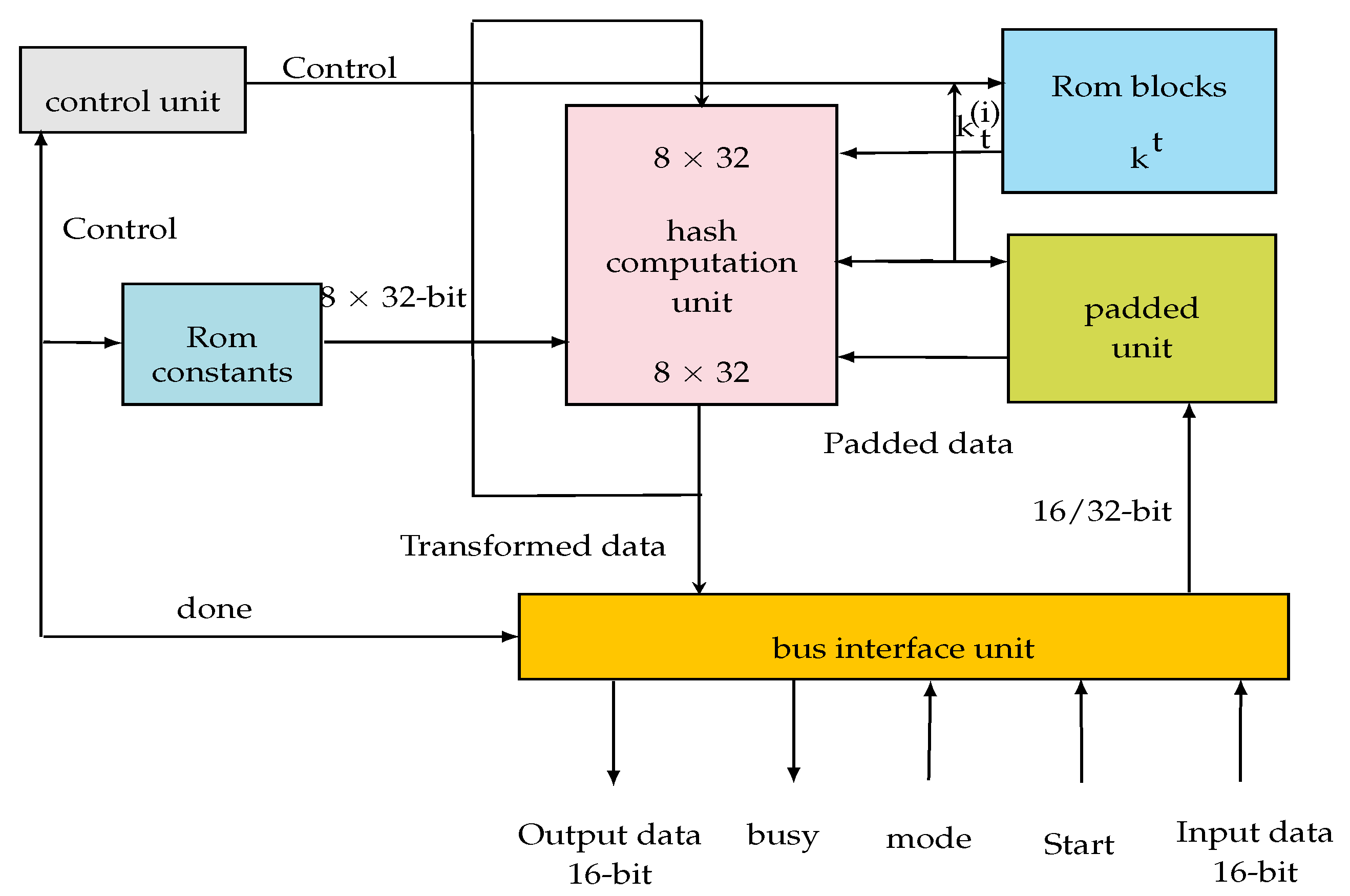
The proposed hardware architecture of the SHA-2 IP is described in Figure 2.
As is shown in Figure 2, our hash processor is based on four modules, which form the overall architecture. They are:
- The control unit: this is designed to control the data flow in the design, as well as the data transfer between the digest calculation unit (hash computation unit) and the pre-processing unit (padded unit). An FSM is used for this purpose. The control unit coordinates all system operations. It defines the necessary constants and the length of the operation word. It manages the ROM blocks and controls all algebraic and digital logic functions necessary to calculate the digest.
- The pre-processing unit (padded unit): its role is to complete the message in order to make it compatible with the used hash protocols.
- The calculation unit (hash computation unit): this is the digest calculation block. It performs the data transformation functions.
- The input/output interface unit has been designed in order to communicate the processor with the external environment.
4.1.2. SHA-2 Architecture Optimization
Different hardware optimizations were done in order to speed-up the SHA-2 IP and decrease area use:
- Addition is the most common operation in calculating the message digest. It requires adding a 64-bit operand size. Therefore, it is important for it to be optimized. Thus, in order to have a fast and low area SHA-2 IP, various time-efficient adder architectures have been developed in VHDL [23], such as the Ripple Carry Adder (RCA), the Carry Look-ahead Adder (CLA), the Carry Save Adder (CSaA) and the Carry Selected Adder (CSeA). Being studied in [24] and implemented on FPGA Virtex-II Pro xc2vp7-5ff672, the RCA adder and the CLA are the best in terms of area occupation on the FPGA platform; whereas, the carry select adder is the most speed efficient.
- In each round of the SHA-2, some operations can be calculated independently and the others are dependent. In [24], the authors changed the expressions A, B, C, D, E, F, G and H in order to optimize the SHA-2 design by condensing two cycles (, ) in the same cycle. Thus, the following round can instantly calculate an intermediate value based on the available inputs by storing the intermediate values of Wt and Kt. The data processing time is reduced by half cycles. The processing algorithm will be different since it reduces the number of cycles (divided by two).
- By changing the expressions of A, B, C, D, E, F, G and H, the number of adders increased from 7 to 14. To solve this problem and analyzing the dependency between hash calculations, two methods were proposed, the first used only two adders and the second used three adders. For the first method, only two adders will be used at each stage of the calculation, the two adders are active. In the second method, just three adders are required in two states. It is clear that both methods have the same speed, so, the first method was adopted in order to decrease area occupation.
4.1.3. Simulation and Synthesis Results of the SHA-2 IP
The SHA-2 IP was implemented on FPGA Virtex2 xc2v2000. Table 1 presents its performance in terms of frequency, speed, slices occupancy and power consumption.
Before optimization, the processor throughput is about 308 Mbit/s. In order to improve the service quality of the IP integrity, the SHA-256 was optimized. In this case, the processor throughput increases up to 584 Mbit/s. The last column in the table gives the algorithmic efficiency of SHA-256 which has the same efficiency before and after optimizations. It is due to the additional tests and the increase number of CLBs. Furthermore, the optimized processor was speeded-up with a reduced variation in the FPGA occupation. Similarly to power, it has also increased but remains low.
4.2. Elliptic Curves Over Finite Fields
This section briefly sums up the theory of elliptic curves. An elliptic curve E over is defined by an equation of the form:
with and .
The elliptic curve is the set of points that verifies the Equation (3) with a point at infinity denoted O. The two main operations in finite field elliptic curves are point addition and point doubling. Let be the first point and be the second point such that , the sum is . The algebraic formula of and are presented by Algorithm 1.
| Algorithm 1: Point Addition and Point Doubling. | |
| Input: | Input: |
| and | |
| Output: | |
| 1. | Output: |
| 2. | 1. |
| 3. | 2. 3. |
| 4. 5. | 4. |
| 6. | 5. |
| 7. | 6. |
| 8. | 7. |
In the next section, the architecture design of the ECC encryption scheme will be presented. The implementation results will be given and discussed.
4.2.1. ECC IP Architecture Design
In order to avoid modular inversion in point addition and point doubling, Lopez and Dahab projective transformation will be used: , , maps to [25]. The security of ECC depends on the ability to compute a point multiplication.
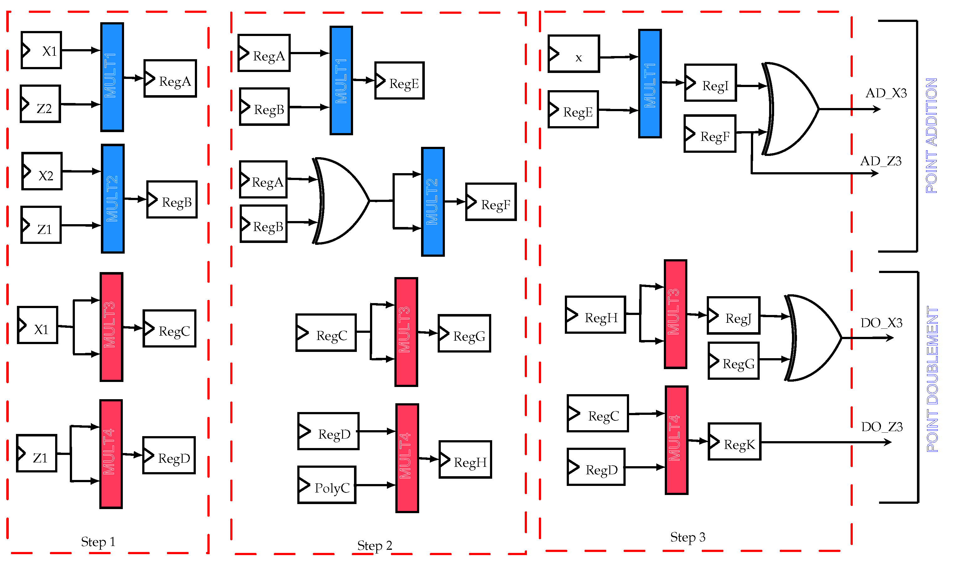
Thus, to perform it, the Montgomery algorithm will be adopted in order to exploit the parallelism of point addition and point doubling which are calculated independently. They are computed at the same time as mentioned in Figure 3. These two basic operations are based on modular arithmetic operations. Indeed, the point addition needs five multiplications and the point doubling needs six multiplications, but, only two multiplications will be used in each operation. The approach here is based on the components full-time function, so, in all modules (point conversions and point operation) only two multipliers are used. They are activated and reactivated in the next step as it is shown in the Figure 3. The component reuse and the components full-time function are the main optimizations in the ECC architecture which presents competitive results compared to the state-of-the-arts. Results and comparison will be given in the next section.
4.2.2. Simulation and Synthesis Results of ECC IP
The ECC IP is based on the Montgomery scalar multiplication over using projective coordinates. The main operations in the Montgomery algorithm are the point addition and the point doubling shown in Figure 3. They were both optimized in order to use only two reused multipliers. Thus, this can increase the IP performance by decreasing the IP consumption and the area occupancy. The ECC implementation results are listed in Table 2.
The proposed ECC-IP was implemented on FPGA Virtex 5 ML 50 and it gave good results. Thus, its performance allows it to be more suitable for ECDSA implementation. Table 3 gives a comparison results with the state-of-the-art implementations.
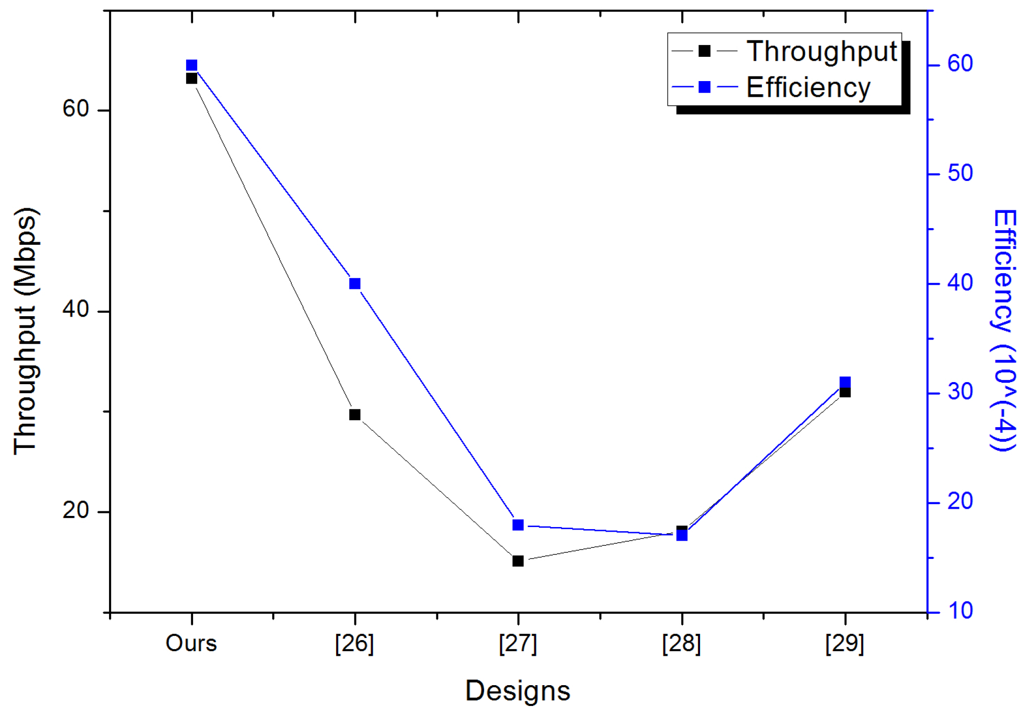
As it is shown in the table below, the implementation in [26] presents a minimal area compared to the proposed ECC architecture while requiring an important execution time at the same time. Thus, the implementation results of the proposed ECC architecture outperform those of the implementation in [28] in terms of area and required time to compute the scalar multiplication. The implementation of [29] is recent, it was done in 2015 using the Virtex5 platform, our proposed ECC architecture presents better results in all parameters. In fact, the area and time are decreased by 6.68% and 49.4% respectively. The last two columns in the table show the algorithmic throughput and efficiency. In order to compare our design to those of the other works we draw the Figure 4 containing both throughput and efficiency values.
Therefore, our proposed ECC design has the highest throughput and efficiency when compared with those of the existing works, because a high throughput requires optimization of the design critical path, the design area, and the design clock cycles number.
4.3. Random Number Generator (RNG)
Generally, asymmetric schemes are based on the level of difficulty of such problem and on the complexity of the used algorithm. However, its security must not only rely on these points but also on the secret of the key which is a parameter used in each implementation [30]. Several problems appear when generating keys:
- Finding the appropriate algorithms for random (or pseudorandom) generation of the bit sequences. The period of these algorithms must be long enough,
- Testing the quality of these binary sequences, which means checking the randomness of the generated bit sequences,
- Generating these keys through deterministic algorithms in order to achieve higher speed and efficiency,
- Protecting these pseudorandom generators against the mathematical and the physical attacks.
- Implementing and optimizing these key generation algorithms in hardware with respect to the platform’s requirements.
There are several methods for hardware key generation, the best known are the Linear Feedback Shift Registers (LFSRs) and the Non Linear Feedback Shift Registers (NLFSRs) generators. The LFSRs can be used for other stream cipher generators such as those used for GSM (A5/1, A5/2 and W7), and the NLFSRs are known as the grain [20]. Table 4 shows the functional characteristics of the mentioned pseudorandom generator which are key length and initialization vector (IV).
The grain-128 supports the 128-bit key and an IV of 96 bits. This encryption is still very small and easy to be implemented in hardware [22]. In addition, the speed in hardware implementation can be easily increased. This is a good characteristic for the grain family compared to other Pseudorandom Number Generators (PRNG).
4.3.1. Security Analyses of PRNG
The generated keys quality is one of the most critical points of configuring a crypto-processor. If the keys are not randomly generated, then an attacker can guess the key. To detect deviations from the randomness of the binary sequences, the National Institute of Standards and Technology (NIST) uses a statistical test suite for random and pseudorandom number generators for cyptographic applications. The NIST test suite is a statistical package which contains 15 different tests that test the randomness of binary sequences produced by cryptographic random or pseudorandom number generators [32]. In our case, the randomness of A5/1, W7, CA, and Grain output’s was tested.
A sequence can be random if the P-value probability for each test is greater than 1% (0.01). The various tests results applied to the algorithms A5/1, W7, CA, and the grain are presented in Table 5. The results presented in this table show that the standard version of the grain outperforms CA, W7, and A5/1 in terms of security. Analyzing these results, the number of keys generated by this version (through the different tests) is always greater than the key’s number generated by CA, W7, and A5/1. For example, the key number tested using Monobit Test with acceptable results is 0.0109 × 2 (≈5 × 0.0022 × 2 for W7 and ≈ 4 2960 × 0.0026 × 2 for A5/1).
By increasing the speed of the grain, the results are less efficient but still better than those given by W7 and A5/1. To conclude, thanks to the non-linear functions, the grain ensures a higher level of security than CA and W7.
4.3.2. Implementation and Synthesis Results of the Pseudorandom Number Generators (PRNG).
The synthesis results of the grain, the A5/1, the W7 and the CA 16 × 16 are presented in Table 6. They were synthesized using the packages of "Synplify Pro" component and the Virtex2 XC2v2000-6ff896 platform.
The A5/1 generator has an acceptable speed with an occupancy rate of 2% and a relatively low consumption ratio. This generator can be used for GSM. The W7 frequency is lower while its period is greater than that of the other generators, which ensures a high-security level. The occupation of the various generators: A5/1, W7 and CA 16 × 16 is very small and similar. The speed of the generators A5/1 and W7 are negligible compared to CA. The throughput increases about 38,113.68 Mbps between CA 16 × 16 and W7. Thus, the use of a higher level of security for the W7 presents a loss in terms of execution time. The W7 and CA 16 × 16 have the maximum efficiency but they have the maximum power consumption. All PRNGs have a low consumption, which makes them the most suitable for use in the restrained environments such as Bluetooth or GSMs. As a conclusion and from the implementation results, the grain generator presents firstly the best trade-off between area, speed, and consumption. Secondly, the grain-128 preserves the advantages of the grain-80, because, it supports a 128-bit key and a 96-bit initialization vector.
4.3.3. The grain IP
From a hardware point of view, the grain is designed to be very small and efficient. It is based on the bit synchronous stream cipher that requires an 80-bit key to initialize its input registers. It is based on two shift registers of fixed size (80 bits) in which the bits are shifted at every clock (LFSR and NLFSR) and a nonlinear output function.
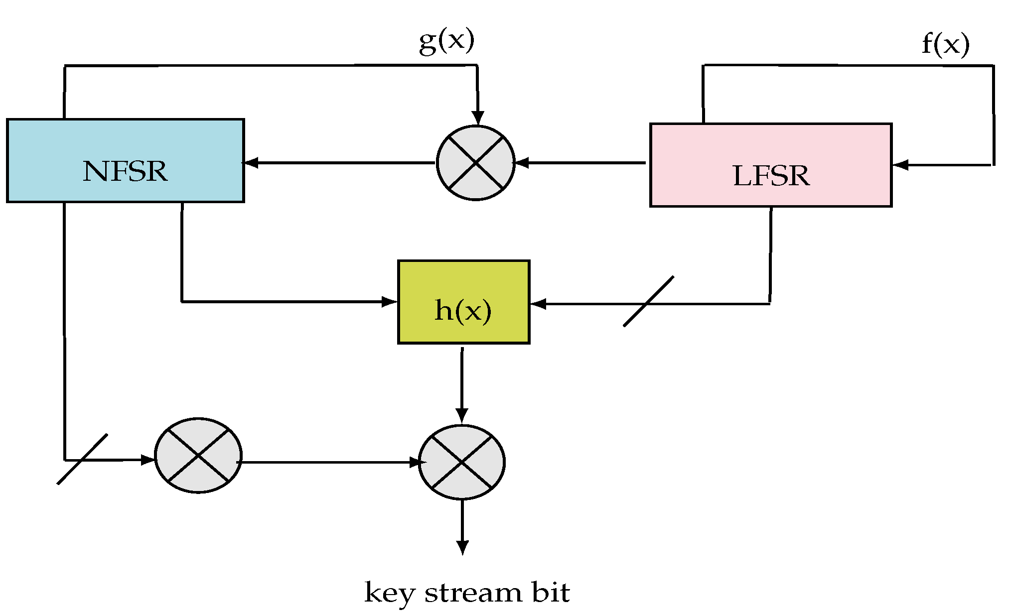
Depending on the used platform, the user can estimate or fix the speed of encryption. Figure 5 shows the grain algorithm. It is based on three modules which are:
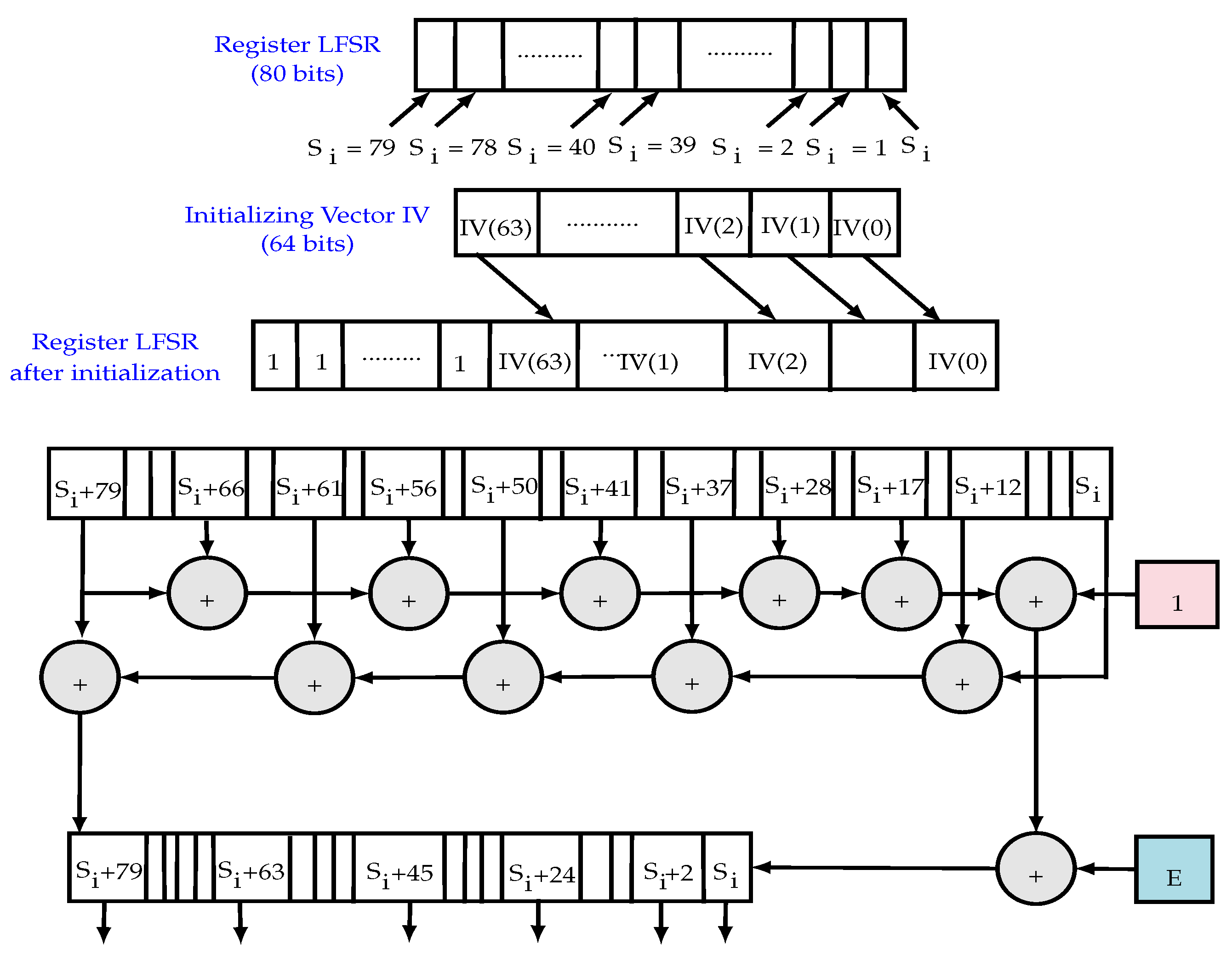
- The LFSR module: based on a sequence () and a linear feedback function. It guarantees a minimum period for the key-stream, so it can be efficiently implemented and it increases significantly the throughput. The polynomial function of the LFSR (feedback polynomial) denoted is a primitive polynomial of degree 80. Figure 6 illustrates the operation of the LFSR block including the register initialization, the polynomial function and the update function.
- The NLFSR module: is a non-linear feedback shift register based on a sequence (). It includes a masked input with the LFSR output in order to balance its state. The NLFSR introduces non-linearity to cipher with the nonlinear output function. It is a filter of a polynomial function .
- The filter module: it is a function of nonlinear output which introduces non-linearity encryption. Based on a nonlinear filtering function () with five input variables, the filter of algebraic degree 3 is selected to be well balanced.
4.3.4. Grain Optimizations
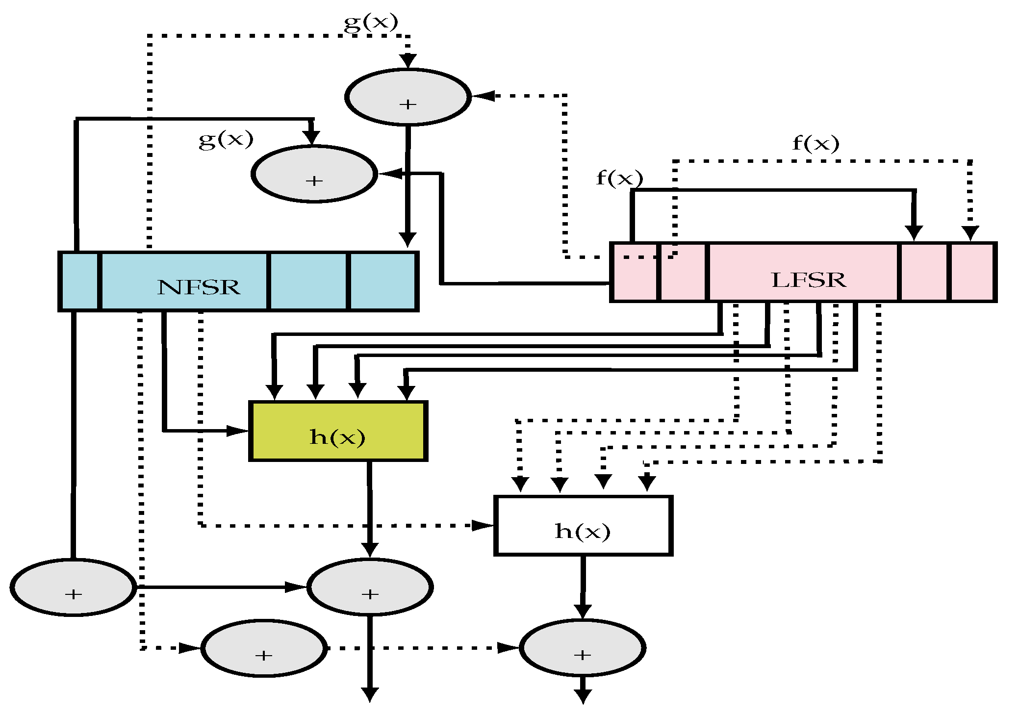
The two registers (LFSR and NLFSR) of the grain are synchronized such that a bit is generated each clock cycle. The grain offers the possibility to increase the speed thanks to the implementation of polynomial functions ( and ) and the filter function () several times. Hence, to simplify this implementation, the last 15 bits of the two shift registers ( and , ) were used neither in and functions, nor in the filter function input [20]. Thus, this can multiply the speed by 16 and reduce the initialization phase required time (160/16 cycles) and the key generation (80/16 cycles). Figure 7 shows a sample implementation: in a doubling, two bits are generated at each clock cycle.
In addition, a generic version of the grain stream cipher was proposed in order to generate a 128-bit key, it allows users to set the speed using a signal of 4 bits. This version is designed for constrained environments where resources are limited and power consumption is reduced. It is based on the same principle as the first version of the grain 80-bit: 2 shift registers LFSR and NLFSR (of size 128 bits) with an output function. Supporting a 128-bit key and a 96-bit initialization vector, the grain-128 preserves the advantages of the grain-80: it ensures height security level, reduced size, and simplicity in implementation. The grain-128 can also offer the possibility of increasing the speed through the implementation of the polynomial functions ( and ) and the filter function () several times. The speed can be multiplied by 32.
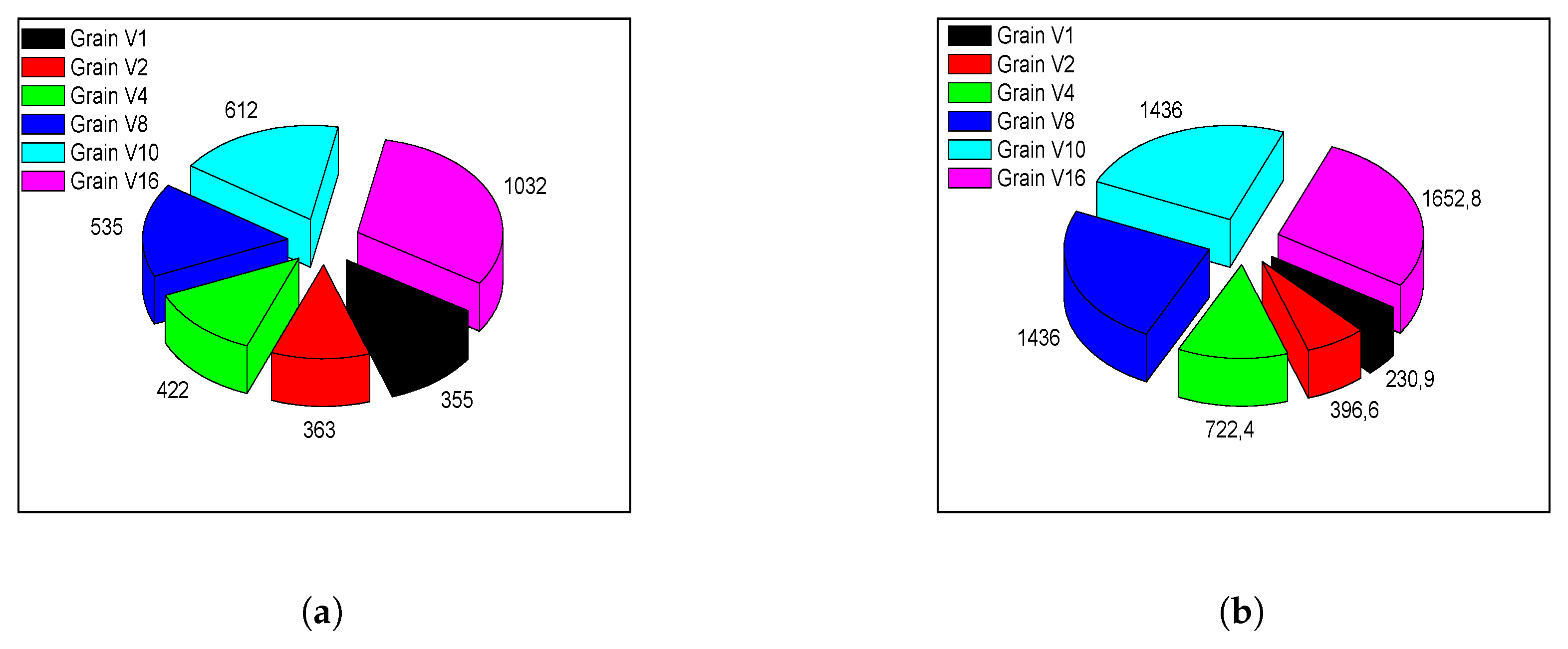
4.3.5. Simulation and Synthesis Results of the Grain IP
The grain was synthesized using the packages of "Synplify Pro" component and the Virtex2 XC2v2000-6ff896 platform. Figure 8a,b illustrate respectively the area occupancy (Luts) and the speed (Mbps). Various versions of the grain-80 were implemented. The grain Vi denotes the grain version i (i indicates the increase of speed). The synthesis of the various versions shows that the speed is proportional to the occupancy and also to the power consumption. It is becoming increasingly significant from one version to another. For example, comparing the standard version of the grain (grain-80) to the grain V16, the consumption variation is negligible compared to the evolution of the speed (1652,8 > 7 × 230,9 Mbps). The generic version of the grain VN (N can be 1, 2, 4, 8, 10, 16) gives the opportunity to choose the compatible version with dedicated applications, but it presents a loss in speed, frequency, and occupation. Thus, the grain VN requires an area of about 4500 Luts achieving a frequency of 44 MHz and consuming 15.95 mW. If we take the example of the version whose speed is equal to 1, the frequency decreases from 230.9 (grain V1) to 44 MHz (grain VN), while the occupancy reaches a value equal to 4500 Luts (≈12 × 355).
The grain generator has a simple algorithm which uses a small number of registers and uses a finite number of iterations to achieve a key. Each version of the grain has its own characteristics, the choice of the appropriate version is based on the application’s constraints. The grain ensures security, it reduces the size and it is simple to be implemented. For this reason, it will be implemented in the ECDSA architecture design which will be detailed in the next section.
5. ECDSA Architecture for Low-Area Low-Power Computing
Optimizations mentioned earlier, applied on different IPs allow designing a low area low-power ECDSA architecture. In this section, the different design modules will be presented.
5.1. Proposed ECDSA Processor Design
To perform ECC digital signature, three algorithms are needed: the key pair generation, the signature generation, and the signature verification. They are given, respectively, by the Algorithms 2–4.
Algorithm 2 is responsible for the generation of the pair of key (public and private), it is based on a good choice of elliptic curve, random selection of integer and the computation of the scalar multiplication.
| Algorithm 2:Private and Public Key Generation. |
| Input: message m, domain parameters () |
| Output: private key d, public key Q |
| 1. Choice of elliptic curve . |
| 2. Choice of a point of order n. |
| 3. Choice of a big integer d, with . |
| 4. Choice of a point (the Montgomery scalar multiplication). |
| Return private key d and public key Q. |
To sign a message m, an entity A follows the steps given by Algorithm 3 with a selected domain parameters. It is based on the scalar multiplication and the hash function.
| Algorithm 3:ECDSA Signature Generation. |
| Input: private key d, message m, domain parameters (), public key |
| Output: signature (r, s) |
| 1. Choice of a random integer k, with . |
| 2. Calculate . |
| 3. Calculate . If , so return to step 1. |
| 4. Calculate . |
| 5. Calculate such that: is cryptographic hash result using SHA-1 or SHA-2 of the message m. |
| 6. Calculate . If , return to step 1. |
| Return (r, s) the signature of the message m |
Algorithm 4 explains how the receiver verifies the signature, it does so by calculating the hash function to obtain the message digest then using the public key of the sender on this message.
| Algorithm 4:ECDSA signature verification. |
| Input: a signature , public key, domain parameters (), message m |
| Output: signature verification or rejection |
| 1. Verify that integer r and s are both in . |
| 2. Calculate such that: is cryptographic hash result using SHA-1 or SHA-2 of the message m. |
| 3. Calculate . |
| 4. Calculate and . |
| 5. Calculate . (using the point addition formula on the elliptic curve). |
| 6. If , so signature will be rejected. Else, calculate . |
| 7. Signature will be accepted only if . |
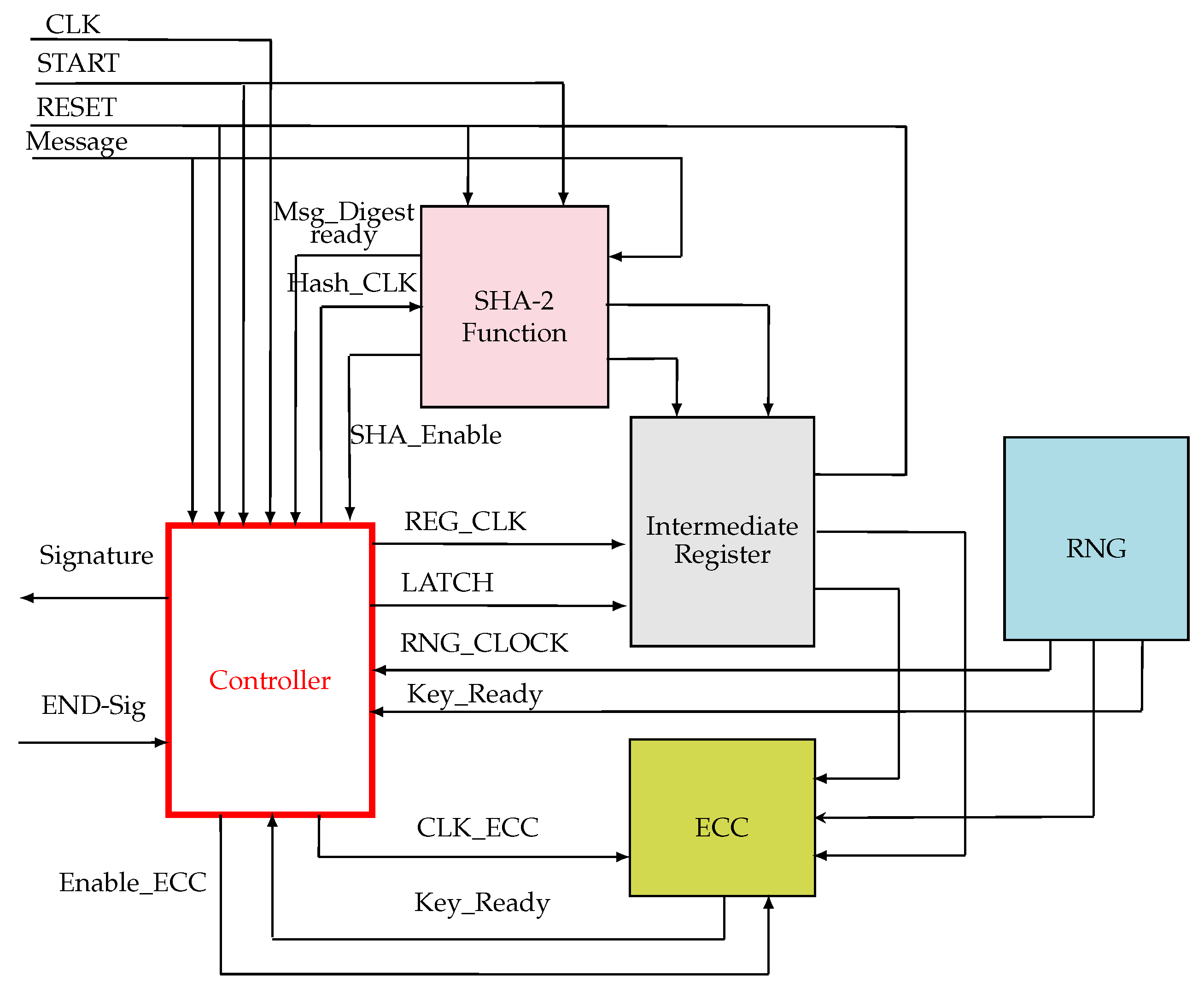
Figure 9 sums up the architecture design of the ECDSA digital signature cryptosystem.
It contains five main units:
- The ECC unit: it computes the point scalar multiplication based on the Montgomery algorithm which was explained in Section 4.2,
- The SHA-2 function unit: generates hash used in both the signature generation and the signature verification of the message m, it was presented in Section 4.1,
- The PRNG unit: it is a random number generator which generates a random number used as keys during the signing process, it was well detailed in Section 4.3,
- The intermediate register: used to store the intermediate results,
- The controller unit: it generates and sends control signals to all units in order to synchronize them. It is totally responsible of the system management and the data exchange between the different units by the use of the control lines.
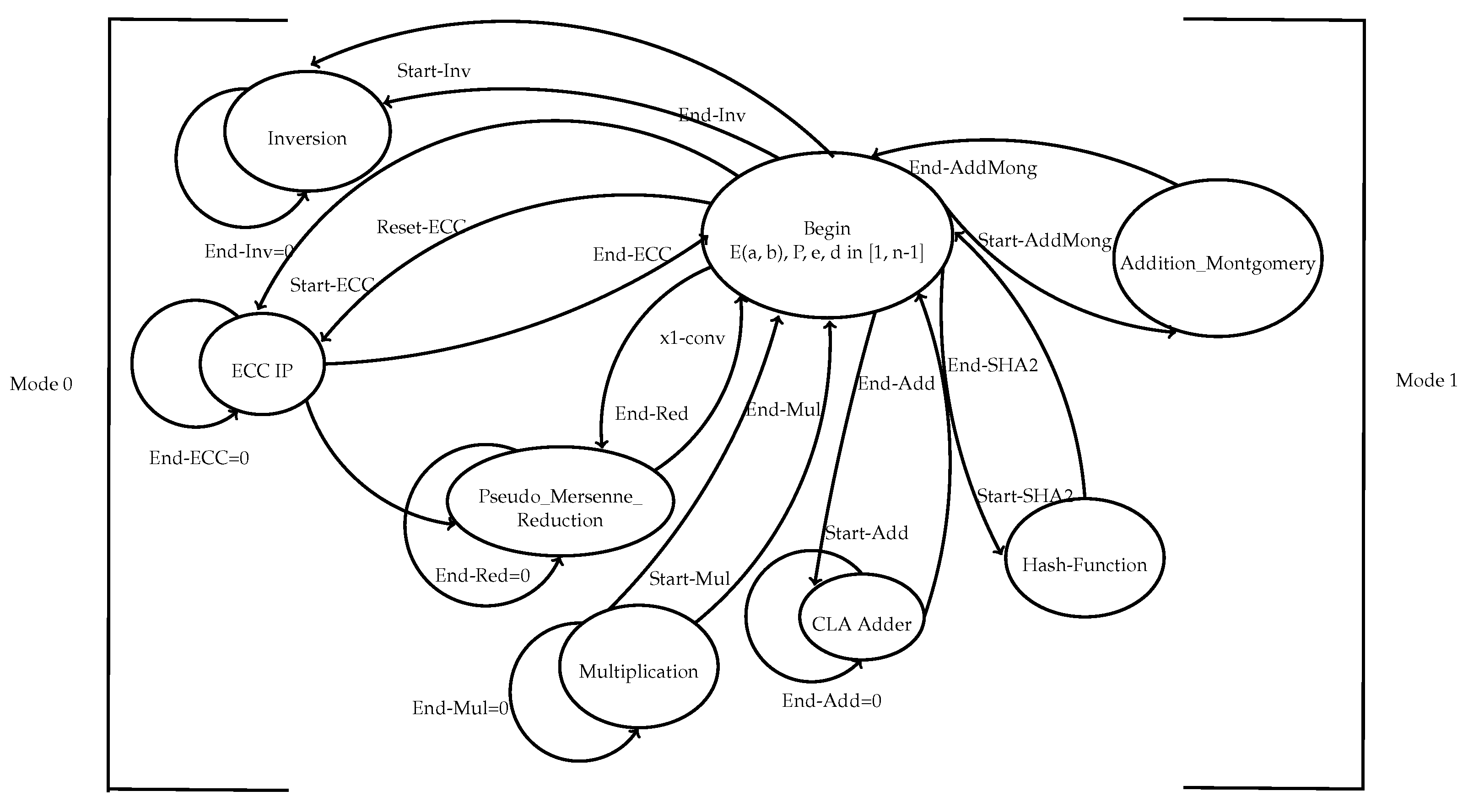
The ECC, the SHA-2 and the random generator IPs were explained earlier. The controller unit is one of the main units in the ECDSA architecture. The interface between the different IPs and registers is ensured through a controller. It is responsible for the synchronization, the sequential activation of the different components, the flow control, and the data dependencies. It is based on a hard synchronous finite state machine represented by Figure 10.
Thus, an efficient hardware implementation needs the synchronization of the different components as shown in the Figure 10. The controller uses two modes: Mode 0 for the key and the signature generation and Mode 1 for the signature verification. All used blocks need two signals: “Start” to begin the computation and “End” to end the computation. The two modes are explained as follows:
- Mode 0: this mode is used for the Key and the signature generation. After the selection of an elliptic curve E(a,b), a point G ∈ E(a,b) of order n and a cryptographically strong random number d which is the private key in the interval [1, n − 1], the controller computes the scalar multiplication using ECC IP: point . It activates the ECC IP by the signals: "Reset-ECC" (enable) and "Start-ECC" (begin the computation). If the signal "End-ECC" = 1, the outputs of the IP-ECC are the coordinates x and y of the public key Q, this is the key generation step. For the signature generation: after selecting a pseudorandom number k, the controller reactivates the ECC-IP as it is mentioned earlier in order to compute . Then, it sends the signal "Start-Red" to the pseudo-Mersenne-reduction block to convert to an integer -conv. After that, the controller tests if -conv = 0, then the step of random number generation will be repeated, else, the controller activates the inversion block, via the signal "Start-Inv", in order to calculate . Here, the inversion and the Mersenne reduction operations are independent, so, they can be done in parallel. Receiving the signal "END-Inv" indicating the end of the inversion, the controller activates the SHA-2 IP. The output of the SHA-2 IP is the message digest e. Receiving the signal "End-SHA2", the controller activates the multiplication operation, by sending the signal "Start-Mul", in order to perform . The Carry Look Ahead Adder (CLA) is used to calculate . The block of multiplication is reactivated to calculate . Computing the second multiplication, the controller tests the value of s, if then return to the step of random number generation, else returns the signature of the message m which is . As it is mentioned, the ECC-IP and the multiplication block are used twice in the Mode 0.
- Mode 1: it is responsible for the signature verification. The inversion block and the SHA-2 IP are reactivated to calculate respectively and . Receiving the signals "End-Inv" and "End-SHA2", the multiplication block is reactivated by the controller to compute firstly and then . After receiving the signal "End-Mul", the controller sends the signal "Start-AddMong" to the Addition-Montgomery block to calculate using the point addition formula on the elliptic curve. The controller tests the value of X: if , so, the signature will be rejected, else, it calculates . Finally, the signature will be accepted only if .
As it is shown in the controller finite state machine explanation, a sequential activation of the IPs and the other required blocks is required. Table 7 presents how the controller activates (ON) and disables (OFF) the different IPs as needed.
The grain, the ECC IP, the SHA-2 IP, and the inversion block are called twice in the entire architecture. And, the multiplication block is reactivated 4 times. As it is mentioned in the table below, independent operations such as hash function SHA-2 and ECC IP can be computed in parallel. In the next section, implementation results of the ECDSA will be given.
6. Implementation Results of ECDSA and Performance Analyses
We implemented FPGA and ASIC designs that efficiently perform ECDSA. The described circuit was implemented in VHDL using the Model Technology’s ModelSim Simulator and synthesized, placed, and routed using target device of Xilinx (Xilinx Virtex5-ML50 FPGA) and ASIC CMOS (45 nm Technology). The architecture was simulated for verification of the correct functionality, by using the test vectors provided by the NIST standard. Performance metrics such as area (slices), frequency (MHz), power consumption (mW), cycle number and the Execution Time (ms) were computed. Detailed implementations results are presented in Table 8.
The FPGA implementation of both the signature + verification requires 167,494 cycles, achieving a maximum frequency of 107.4 MHz in 1.5 ms of time. The signature needs only 84,000 cycles and it runs in 782 s. It consumes about 94.25 (mW). The throughput of the ECDSA is about 0.16 Mbps and the efficiency is 88 × 10−5. Table 9 gives a comparison between the proposed ECDSA scheme and the state-of-the-art results.
As it is shown in the table below, the proposed design (FPGA implementation) is about 60% faster than [33]. Being compared to [2], our results outperform B. Panjwani et al. results in terms of area and frequency. In addition, our architecture presents a gain of about 22% and 57% in terms of area and execution time. Comparing our results to those of [34], we have decreased the area by 22.12 % and the execution time by 57.54%. Being implemented in ASIC platform, our design has minimal area than that reported in [34].
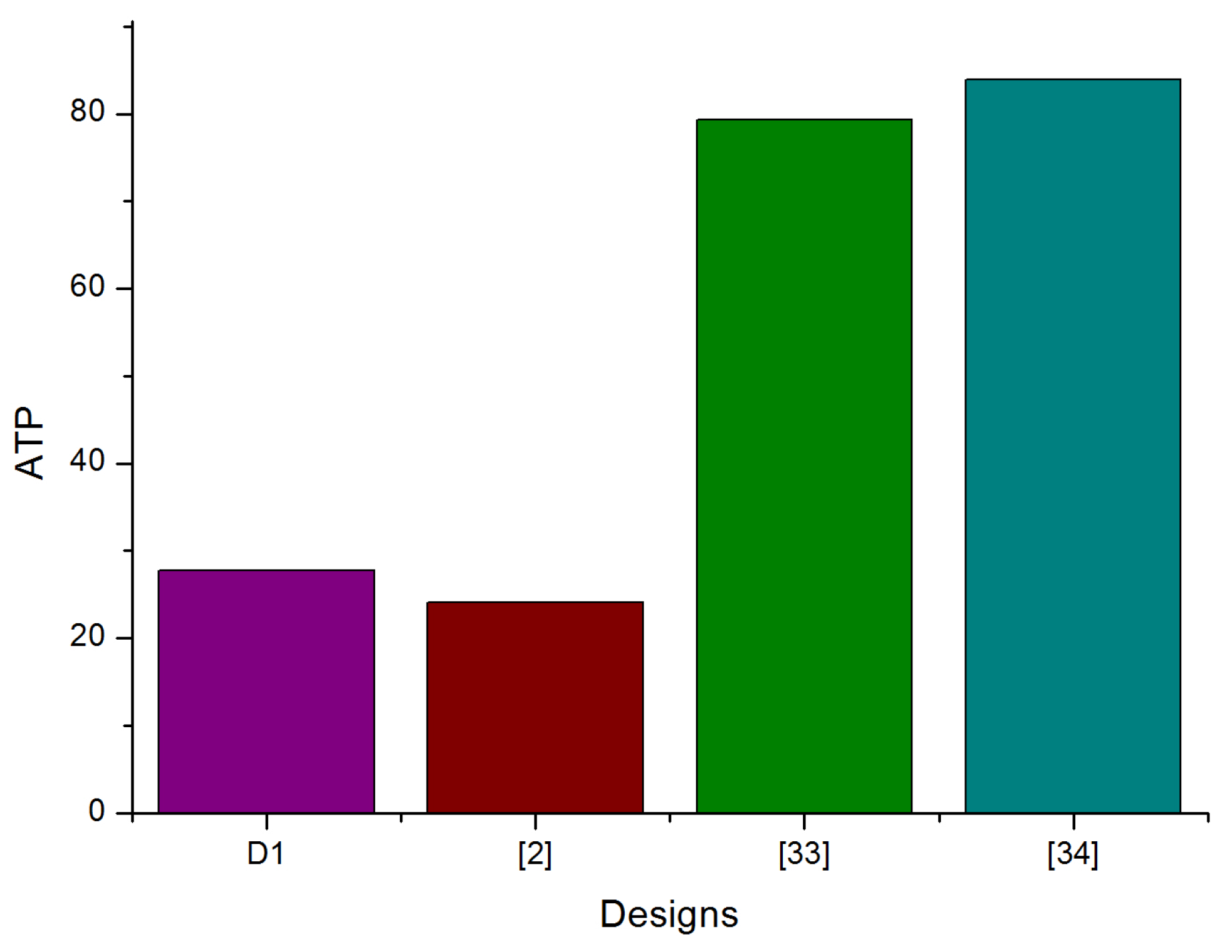
In order to have a relevant performance comparison between our synthesis results and those of related works, we will add another parameter which is the Area Time Product (ATP). Figure 11 gives different ATP of the mentioned state-of-the-art FPGA implementations.
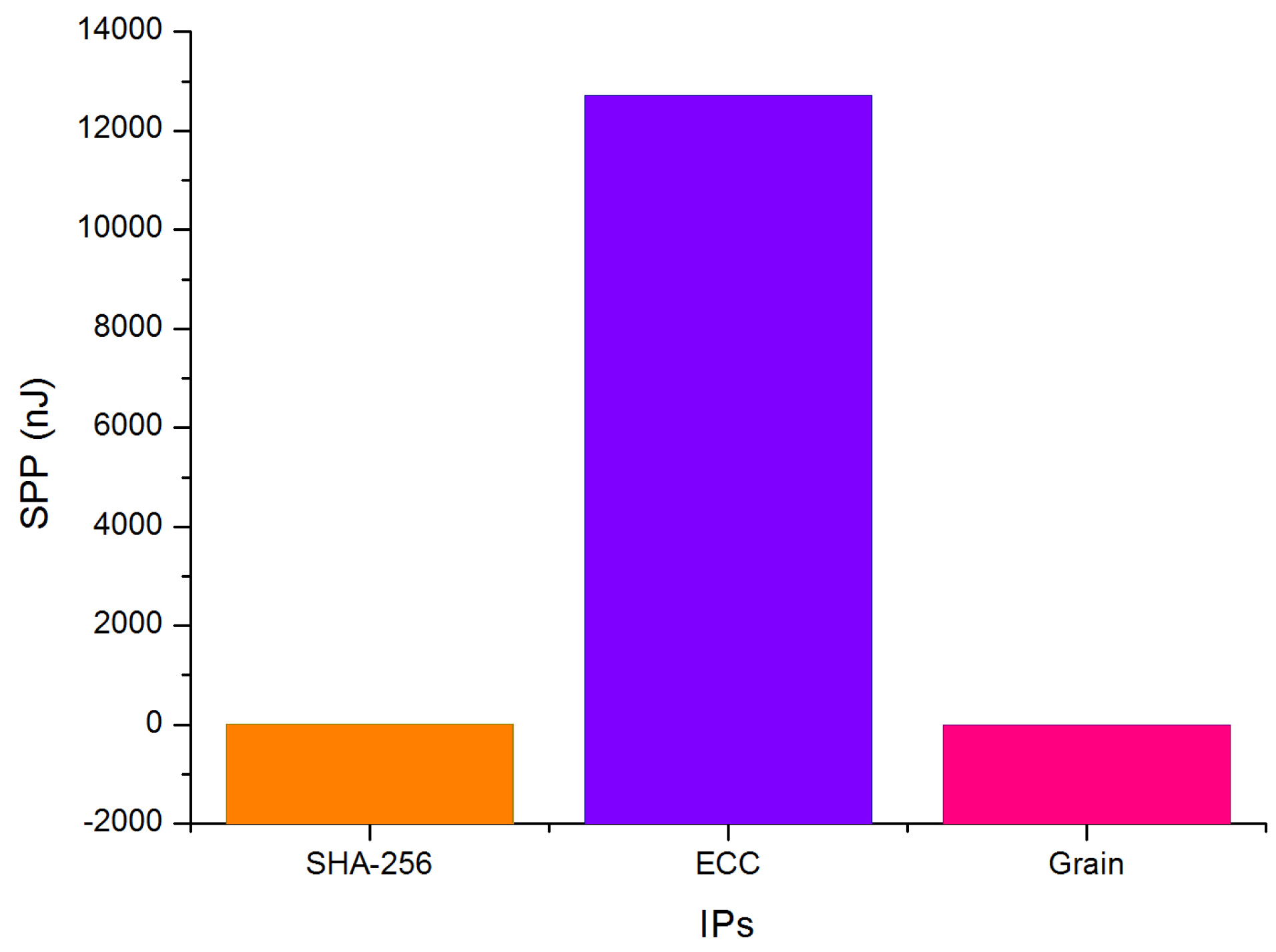
It is clear from Figure 11 that our design and the design in [2] have the minimum value of ATP. Our designs (, ) have a trade-off between area and time and it is the most efficient compared to other designs. In the literature, only a small number of authors have given the power dissipation of the ECDSA entire design. For this reason, in order to study the influence of the power, we have draw Figure 12 containing all the SPP (Speed Power Product) of all IPs.
The SPP is calculated by multiplying the gate propagation delay by the power dissipation. As it is shown in Figure 12, the ECC-IP has the highest SPP value.
7. Security Analyses of ECDSA Processor
Several interpretations have been reported of what it means to break a digital signature: retrieving the secret key, creating another signing algorithm with an equivalent secret key, forging a signature for a chosen message, and forging a signature for at least one message [36]. In order to be useful, ECDSA must have a high security. The essential security conditions for ECDSA are [37]:
- To ensure that one cannot easily solve the discrete logarithm problem and therefore obtain the secret key,
- The hash function used is a one-way collision-resistant hash function.
- The secret key can be obtained using k, r, and s when the generator for k is predictable.
The Elliptic Curve Discrete Logarithm Problem (ECDLP) is a special case of the discrete logarithm problem. It consists of finding an integer d, if it exists, such that , given points G, Q ∈ E(). Many attacks against ECDLP exist such as the exhaustive search, the Pohlig-Hellman, and the Baby-Step Giant-Step algorithms. One of these attacks is the Pollard’s Rho algorithm, which has a running time of where n is the order of point G. However, this algorithm can be parallelized and run on r different processors, so that the new running time is .
In this section, two attacks against ECDSA processor have been chosen: fault injection attack and restart attack.
7.1. Fault Injection Attack: No Correctness Check for Input Points
This attack is applicable when the device neither explicitly checks whether an input point P nor the result of the computation really is a point on the cryptographically strong elliptic curve E which is a parameter of the system. The no correctness check for input points attack is simple and should not be applicable to a well-designed system, but nevertheless, such a “bug” might happen in practice. Let , , , , be a given cryptographically strong elliptic curve, which is part of the setup of the ECC system. The coefficients are in a field K and denotes the set of all solutions (x, y) , together with the point at infinity O. We note that when calculating a scalar multiplication, the coefficient is not used. In this situation when a cryptosystem receives a point , with , but is not a point on E, but a point on some other elliptic curve .
We choose the input pair , carefully, such that with the tipple (, , , , ) defines an elliptic curve whose order has a small divisor r and such that ord(P) = r. If r is relatively small, the attacker can solve the discrete logarithm problem in the subgroup of order r and find . We can repeat this procedure with a different choices of P and use the Chinese Remainder Theorem to compute the correct value of k.
In particular, an attack is possible by injecting any fault on the coordinates x or y point P. With stronger assumptions, the attacker can even find the secret k having injected any fault on the two coordinates. This attack is quite efficient if we do not choose , but the curve first and compute . To avoid fault injection attack in the scalar multiplication, a point P must be a valid point on the curve, as it is advised in the protocols of most ECC.
7.2. Restart Attack
In this part, we present our results on an ECDSA signature generation against the restart attack. To break the scheme with signatures of two different messages we assume that the pseudorandom generator for the key k is deterministic. Then assume that one can reset the internal state of the generator. So, if the signer signs by generating k and we can reset it so that it generates the same k for , we have a signature (r, ) for and a signature (r, ) for . Hence we obtain that:
Accordingly, using the chaos-based key generator affects the resistivity of the proposed ECDSA cryptosystem to the restart attack because the initial key value of the grain key generator is modified for each signature generation. In order to improve the sensitivity of the signature processor to the initial key, we maximized the use of the chaos generation of the key in the inter-functions of the grain pseudorandom generator. Thus, the initial key value of the grain is not constant. Instead, it is formed from the initial chaos generated key.
8. Conclusions and Future Works
In this paper, an ECDSA signature scheme was implemented. All integrated IPs (ECC, SHA-2, and the grain) were optimized in order to lead to a trade-off between area and execution time. Thus, the implementation results, in both Virtex-5 and ASIC, are competitive with those of the state-of-the-art. The signature and the verification processor used 18,504 slices in Virtex-5 achieving a frequency of 107.4 in 1.5 s. Being implemented on an ASIC CMOS 45 nm technology, the design requires 0.257 mm area cell achieving a maximum frequency of 532 MHz and consumes 63.444 (mW). The proposed ECDSA implementation is suitable for applications that need: low-bandwidth communication, low-storage and low-computation environments such as embedded systems. As we said earlier, the design overhead costs should be reduced to be suitable for applications which require low area resources. As a future work, ECC-IP can be again optimized by introducing the procedure of Secure Hardware Activation System (SEHAS) and the Physically Unclonable Functions (PUF) [38].
Acknowledgments
We did not receive funds for covering the costs to publish in open access.
Author Contributions
Anissa Sghaier, Medien Zeghid, Chiraz Massoud and Mohsen Machhout conceived the design. Anissa Sghaier and Medien Zeghid implemented the design, analyzed the results, and wrote the paper.
Conflicts of Interest
The authors declare no conflict of interest.
References
- The FIPS 186-4 Elliptic Curve Digital Signature Algorithm Validation System (ECDSA2VS). Available online: http://csrc.nist.gov/groups/STM/cavp/documents/dss2/ecdsa2vs.pdf (accessed on 18 March 2014).
- Panjwani, B.; Mehta, D.C. Hardware-software Co-design of elliptic curve digital signature algorithm over binary fields. In Proceedings of the International Conference on Advances in Computing, Communications and Informatics (ICACCI), Kochi, India, 10–13 August 2015; pp. 1101–1106. [Google Scholar] [CrossRef]
- Montgomery, P.L. Speeding the pollard and elliptic curve methods of factorization. Math. Comput. 1987, 48, 177–243. [Google Scholar] [CrossRef]
- National Institute of Standards and Technology. Secure hash standard. In Federal Information Processing Standards 180-2; Federal Information Processing Standards Publications (FIPS PUBS): USA, 2002. [Google Scholar]
- Petit, J.; Sabatier, P. Analysis of ECDSA authentication processing in VANETs. In Proceedings of the IEEE 3rd International Conference on New Technologies, Mobility and Security, Cairo, Egypt, 20–23 December 2009; pp. 388–392. [Google Scholar] [CrossRef]
- Khalique, A.; Singh, K.; Sood, S. Implementation of elliptic curve digital signature algorithm. Int. J. Comput. Appl. 2010, 2, 21–27. [Google Scholar] [CrossRef]
- Nabil, G.; Naziha, K.; Lamia, F.; Lotfi, K. Hardware implementation of elliptic curve digital signature algorithm (ECDSA) on Koblitz curves. In Proceedings of the 8th International Symposium on Communication Systems, IEEE Networks and Digital Signal Processing (CSNDSP), Poznan, Poland, 18–20 July 2012; pp. 1–6. [Google Scholar] [CrossRef]
- Belgarric, P.; Fouque, P.A.; Macario-Rat, G.; Tibouchi, M. Side-channel analysis of weierstrass and koblitz curve ecdsa on android smartphones. In Proceedings of the Cryptographers’ Track at the RSA Conference on Topics in Cryptology CT-RSA, San Francisco, CA, USA, 29 February–4 March 2016; Volume 9610, pp. 236–252. [Google Scholar] [CrossRef]
- Biswas, S.; Misic, J. A cross-layer approach to privacy-preserving authentication in wave-enabled vanets. IEEE Trans. Veh. Technol. 2013, 62, 2182–2192. [Google Scholar] [CrossRef]
- Plos, T.; Hutter, M.; Feldhofer, M.; Stiglic, M.; Cavaliere, F. Security-enabled near-field communication tag with flexible architecture supporting asymmetric cryptography. IEEE Trans. Very Large Scale Integr. (VLSI) Syst. 2013, 21, 1965–1974. [Google Scholar] [CrossRef]
- Gueron, S.; Krasnov, V. Fast prime field elliptic-curve cryptography with 256-bit primes. J. Cryptogr. Eng. 2015, 5, 141–151. [Google Scholar] [CrossRef]
- Pessl, P.; Hutter, M. Curved tags-a low-resource ecdsa implementation tailored for RFID. In Proceedings of the 10th International Workshop, RFIDSec, Revised Selected Papers Radio Frequency Identification: Security and Privacy Issues, Oxford, UK, 21–23 July 2014; Volume 8651, pp. 156–172. [Google Scholar] [CrossRef]
- Liu, Z.; Liu, D.; Zou, X.; Lin, H.; Cheng, J. Design of an elliptic curve cryptography processor for RFID tag chips. Sensors 2014, 14, 17883–17904. [Google Scholar] [CrossRef] [PubMed]
- Yuan, J.S.; Xu, Y.; Yen, S.D.; Bi, Y.; Hwang, G.W. Hot carrier injection stress effect on a 65 nm LNA at 70 GHz. IEEE Trans. Devices Mater. Reliab. 2014, 14, 931–934. [Google Scholar] [CrossRef]
- Yuan, J.S.; Bi, Y. Process and temperature robust voltage multiplier design for RF energy harvesting. Microelectron. Reliab. 2014, 55, 107–133. [Google Scholar] [CrossRef]
- Pan, W.; Zheng, F.; Zhao, Y.; Zhu, W.T.; Jing, J. An efficient elliptic curve cryptography signature server with GPU acceleration. IEEE Trans. Inf. Forensics Secur. 2017, 12, 111–122. [Google Scholar] [CrossRef]
- Bi, Y.; Yuan, J.S.; Jin, Y. Beyond the interconnections: Split manufacturing in RF designs. Electronics 2015, 4, 541–564. [Google Scholar] [CrossRef]
- Alasad, Q.; Bi, Y.; Yuan, J.S. E2LEMI: Energy-efficient logic encryption using multiplexer insertion. Electronics 2017, 6, 16. [Google Scholar] [CrossRef]
- Wang, X.; Yin, Y.L.; Yu, H. Finding Collisions in the Full SHA-1. In Proceedings of the 25th Annual International Cryptology Conference, Santa Barbara, CA, USA, 14–18 August 2005; Springer; Volume 3621, pp. 17–36. [Google Scholar]
- Hell, M.; Johansson, T. Grain: A stream cipher for constrained environments. Int. J. Wirel. Mob. Comput. 2007, 2, 86–93. [Google Scholar] [CrossRef]
- Kanso, A.A. An efficient cryptosystem Delta for stream cipher applications. Comput. Electr. Eng. 2009, 35, 126–140. [Google Scholar] [CrossRef]
- Mansouri, S.S.; Dubrova, E. An improved hardware implementation of the grain stream cipher. In Proceedings of the 13th Euromicro Conference on Digital System Design: Architectures, Methods, and Tools (DSD), Lille, France, 1–3 September 2010; pp. 433–440. [Google Scholar]
- El hadj youssef, W.; Zeghid, M.; Machhout, M.; Rached, T. Design and performance testing of arithmetic operators library for cryptographic applications. Int. J. Comput. Sci. Eng. Syst. (IJCSES) 2007, 1, 201–212. [Google Scholar]
- Zeghid, M.; Bouallegue, B.; Machhout, M.; Baganne, A.; Tourki, R. Architectural design features of a programmable high throughput reconfigurable SHA-2 Processor. J. Inf. Assur. Secur. 2008, 2, 147–158. [Google Scholar]
- Sghaier, A.; Zeghid, M.; Bouallegue, B.; Baganne, A.; Machhout, M. Area-time efficient hardware implementation of elliptic curve cryptosystem. arXiv, 2015; arXiv:0710.4810 [cs.CR]. [Google Scholar]
- Sutter, G.; Deschamps, J.; Imana, J. Efficient elliptic curve point multiplication using digit-serial binary field operations. IEEE Trans. Ind. Electron. 2013, 60, 217–225. [Google Scholar] [CrossRef]
- Roy, S.; Rebeiro, C.; Mukhopadhyay, D. Theoretical modeling of elliptic curve scalar multiplier on LUT-based FPGAs for area and speed. IEEE Trans. VLSI Syst. 2013, 21, 901–909. [Google Scholar] [CrossRef]
- Liu, S.; Ju, L.; Cai, X.; Jia, Z.; Zhang, Z. High Performance FPGA implementation of elliptic curve cryptography over binary fields. In Proceedings of the IEEE 13th International Conference on Trust, Security and Privacy in Computing and Communications (TrustCom), Beijing, China, 24–26 September 2014; pp. 148–155. [Google Scholar] [CrossRef]
- Khan, Z.U.A.; Benaissa, M. High speed ECC implementation on FPGA over GF(2m). In Proceedings of the International Conference on Field-programmable Logic and Applications (FPL), Lausanne, Switzerland, 2–4 September 2015; pp. 1–6. [Google Scholar] [CrossRef]
- Kerckhoffs, A. La cryptographie militaire. J. Sci. Mil. 1883, IX, 5–38. [Google Scholar]
- Rodrigues, J.M. Transfert sécurisé d’images par combinaison de techniques de compression, cryptage et marquage. Thèse Soutenue, Université Montpellier II, Montpellier, France, 2006. [Google Scholar]
- Rukhin, A.; Soto, J.; Nechvatal, J.; Smid, M.; Barker, E.; Leigh, S.; Levenson, M.; Vangel, M.; Banks, D.; Heckert, A.; et al. A Statistical Test Suite for Random and Pseudo-Random Number Generator for Cryptographic Applications. Available online: http://nvlpubs.nist.gov/nistpubs/Legacy/SP/nistspecialpublication800-22r1a.pdf (accessed on 19 June 2017).
- Elhadjyoussef, W.; Benhadjyoussef, N.; Machhout, M.; Rached, T. Low power elliptic curve digital signature design for constrained devices. Int. J. Secur. (IJS) 2012, 6, 2. [Google Scholar]
- Ben Hadj Youssef, N.; El Hadj Youssef, W.; Machhout, M.; Tourki, R.; Torki, K. A low-resource 32-bit datapath ECDSA design for embedded applications. In Proceedings of the International Carnahan Conference on Security Technology (ICCST), Rome, Italy, 13–16 October 2014; pp. 1–6. [Google Scholar]
- Knezevic, M.; Nikov, V.; Rombouts, P. Low-latency ECDSA signature verification a road towards safer traffic. Cryptol. ePrint Arch. 2014, 24, 3257–3267. [Google Scholar] [CrossRef]
- Vanstone, S.A. Next Generation Security for Wireless: Elliptic Curve Cryptography, 2003. Available online: http://www8.cs.umu.se/kurser/5DV153/HT14/literature/vanstone2003next.pdf (accessed on 19 June 2017).
- Vaudenay, S. The Security of DSA and ECDSA. In International Workshop on Public Key Cryptography PKC 2003: Public Key Cryptography-PKC; Springer: Berlin/Heidelberg, Germany; Miami, FL, USA, 2003; Volume 2567, pp. 309–323. [Google Scholar]
- Parrilla, L.; Castillo, E.; Morales, P.D.; Garcia, A. Hardware activation by means of PUFs and elliptic curve cryptography in field-programmable devices. Electronics 2016, 5, 5. [Google Scholar] [CrossRef]
Figure 1.
The proposed methodology and flow design of the Elliptic Curve Digital Signature Algorithm (ECDSA).
Figure 1.
The proposed methodology and flow design of the Elliptic Curve Digital Signature Algorithm (ECDSA).

Figure 2.
The proposed SHA-2 IP.

Figure 3.
Parallelism between the point addition and the point doubling.

Figure 4.
Throughput and efficiency comparison.

Figure 5.
The Grain Design.

Figure 6.
Linear Feedback Shift Register (LFSR) Model Function.

Figure 7.
Doubling-speed Grain Scheme.

Figure 8.
The Grain Performances. (a) Grain version area occupancy; (b) Grain version speed.

Figure 9.
Proposed ECDSA Architecture.

Figure 10.
The controller finite state machine.

Figure 11.
FPGA Implementation ATP.

Figure 12.
FPGA Implementation SPP of the proposed IPs.


Table 1.
SHA-2 Performances.
| Modules | Cycles | Frequency | Area | Power | Throughput | Efficiency |
|---|---|---|---|---|---|---|
| (MHz) | (Slices) | (mW) | (Mbit/s, Slices) | |||
| Implementation without optimization | ||||||
| SHA-256 | 64 | 77 | 773 | 39 | 308 | 0.398 |
| Implementation with optimizations | ||||||
| SHA-256 | 32 | 73 | 1480 | 50 | 584 | 0.394 |
Table 2.
ECC Performances over .
| Area | Frequency | Time | Power | |
|---|---|---|---|---|
| Slices | MHz | s | mW | |
| ECC over | 9670 | 147.5 | 282.79 | 45 |
Table 3.
ECC Implementation results comparison.
| Designs | Curve | FPGA | Clock | Area | Freq. | Time | Throughput | Efficiency |
|---|---|---|---|---|---|---|---|---|
| Cycles | Slices | (MHz) | (s) | (Mbps) | ||||
| This work | virtex5ML50 | 380 | 9670 | 221 | 2.58 | 63.17 | 0.0060 | |
| ECC [26] | Virtex5 | 1371 | 6150 | 250 | 5.48 | 29.7 | 0.0040 | |
| ECC [27] | Virtex5 | 1414 | 8095 | 131 | 10.70 | 15.1 | 0.0018 | |
| ECC [28] | XC4VLX200 | 1091 | 10,417 | 121 | 9.00 | 18.1 | 0.0017 | |
| ECC [29] | Virtex5 | 780 | 10,363 | 153 | 5.10 | 31.97 | 0.0031 |
Table 4.
Functional characteristics of the pseudorandom generator.
| Encryption Algorithms | Key Length (Bit) | Initialization Vector (Bit) |
|---|---|---|
| RC4 | 8-2048 | 8 |
| MUGI | 128 | 128 |
| A5/1 | 64 | 114 |
| W7 | 128 | 128 |
| CA 16 × 16 | 256 | 16 |
| Grain-80 | 80 | 64 |
| Grain-128 [31] | 128 | 96 |
Table 5.
Statistical Test Analyses for Pseudorandom Number Generators.
| Statistical TEST | Pseudorandom Number Generators | ||||
|---|---|---|---|---|---|
| A5/1 | W7 | CA | Grain-80 | Grain-128 | |
| Monobit | 0.0026 × | 0.0022 × × | 0.0025 × | 0.0109 × | 0.0178 × |
| Frequency | 0.0028 × | 0.0016 × | 0.0018 × | 0.0101 × | 0.0168 × |
| Runs | 0.0049 × | 0.0046 × | 0.0045 × | 0.0131 × | 0.0196 × |
| Longest-Run | 0.0021 × | 0.0025 × | 0.0010 × | 0.012 × | 0.0182 × |
| Matrix Rank | 0.0012 × | 0.0012 × | 0.0013 × | 0.0102 × | 0.0136 × |
| DFT (Spectral) | 0.0009 × | 0.00095 × | 0.0015 × | 0.0098 × | 0.0112 × |
| Non-overlapping | 0.00085 × | 0.0011 × | 0.0009 × | 0.0095 × | 0.0119 × |
| Template Matching | |||||
| Overlapping Template | 0.00092 × | 0.0027 × | 0.0012 × | 0.0101 × | 0.0123 × |
| Matching | |||||
| Universal Statistical | 0.0023 × | 0.0036 × | 0.0027 × | 0.0125 × | 0.0161 × |
| Linear Complexity | 0.0012 × | 0.0015 × | 0.0017 × | 0.0107 × | 0.0132 × |
| Serial | 0.0035 × | 0.0026× | 0.0031 × | 0.0099 × | 0.0111 × |
| Approximate Entropy | 0.0017 × | 0.0041 × | 0.0021 × | 0.012 × | 0.0143 × |
| Cusums | 0.0011 × | 0.0035 × | 0.0033 × | 0.0112 × | 0.0117× |
| Random Excursions | 0.0027 × | 0.0022 × | 0.0023 × | 0.0108 × | 0.0123 × |
| Random Excursions | 0.0031 × | 0.0033 × | 0.0015 × | 0.0125 × | 0.0135 × |
| Variant | |||||
Table 6.
Synthesis results of the different Pseudorandom Number Generator (PRNG).
| PRNG | Frequency | Area | Consumption | Throughput | Efficiency |
|---|---|---|---|---|---|
| (MHz) | (Luts) | (mW) | (Mbps) | ||
| Grain-80 | 230.9 | 355 (3%) | 13.72 | 230.9 | 0.65 |
| Grain-128 | 238.5 | 495 (4%) | 19.22 | 238.5 | 0.48 |
| A5/1 | 250.376 | 110 (1%) | 46.33 | 250.376 | 2.27 |
| W7 | 188.590 | 777 (7%) | 111.77 | 1508.72 | 1.94 |
| CA 16 × 16 | 308.550 | 683 (6%) | 52.75 | 39,622.4 | 58.011 |
Table 7.
ECDSA IPs methodology function.
| Grain IP | SHA-2 IP | ECC IP | Pseudo- Mersenne- Reduction | Inversion | Multiplication | CLA | Addition Montgomery | |
|---|---|---|---|---|---|---|---|---|
| Key Generation | ON | OFF | OFF | OFF | OFF | OFF | OFF | OFF |
| OFF | OFF | ON | OFF | OFF | OFF | OFF | OFF | |
| Signature Generation | ON | OFF | OFF | OFF | OFF | OFF | OFF | OFF |
| OFF | ON | ON | OFF | OFF | OFF | OFF | OFF | |
| OFF | OFF | OFF | ON | OFF | OFF | OFF | OFF | |
| OFF | OFF | OFF | OFF | ON | ON | OFF | OFF | |
| OFF | OFF | OFF | OFF | OFF | OFF | ON | OFF | |
| OFF | OFF | OFF | OFF | OFF | ON | OFF | OFF | |
| Signature Verification | OFF | ON | OFF | OFF | ON | OFF | OFF | OFF |
| OFF | OFF | OFF | OFF | OFF | ON | OFF | OFF | |
| OFF | OFF | OFF | OFF | OFF | ON | OFF | OFF | |
| OFF | OFF | OFF | OFF | OFF | OFF | OFF | ON |
Table 8.
ECDSA Crypto-processor implementation results.
| FPGA Implementation | |||
|---|---|---|---|
| Designs | Area | Frequency | Power |
| (Slices) | (MHz) | (mW) | |
| SHA-256 | 1480 | 73 | 50 |
| ECC | 9670 | 147.5 | 45 |
| Grain-128 | 495 | 238.5 | 19.22 |
| ECDSA | 18,504 | 107.4 | 105 .7 |
| ASIC Implementation | |||
| Designs | Area cell | Frequency | Total dynamic Power |
| (mm) | (MHz) | (mW) | |
| SHA-256 | 0.023 | 1282 | 18.4070 |
| ECC | 0.121 | 990 | 39 |
| Grain128 | 0.006572 | 1695 | 6.404 |
| ECDSA | 0.257 | 532 | 63.444 |
Table 9.
Results Comparison of different ECDSA implementations.
| FPGA Implementation Results | ||||||||
|---|---|---|---|---|---|---|---|---|
| Design | Platform | Field | Freq. | Area | Time | Power | Through. | Eff. |
| (Bits) | (MHz) | (Slices) | (ms) | (mW) | (Mbps) | |||
| Virtex-5 | ) | 107.4 | 18,504 | 1.5 | 199.95 | 0.16 | 88 × 10 | |
| [2] | Virtex-6 | 100 | 18,740 | 1.287 | - | - | - | |
| [33] | Virtex-5 | ) | 148.963 | 20,628 | 3.844 | 228 | - | - |
| [34] | Virtex-5 | 195.309 | 23,760 | 3.533 | - | - | - | |
| ASIC Implementation Results | ||||||||
| Design | Platform | Field | Freq. | Area | Power | Through. | Eff. | |
| (Bits) | (MHz) | (mW) | ||||||
| ASIC 45 nm | 532 | 0.257 mm | 63.444 | 0.81 | 3.16 | |||
| [35] | ASIC 45 nm | 500 | 322.1 KGE | - | - | - | ||
| [34] | ASIC 45 nm | 500 | 1.135 mm | - | - | - | ||
© 2017 by the authors. Licensee MDPI, Basel, Switzerland. This article is an open access article distributed under the terms and conditions of the Creative Commons Attribution (CC BY) license (http://creativecommons.org/licenses/by/4.0/).
Share and Cite
MDPI and ACS Style
Sghaier, A.; Zeghid, M.; Massoud, C.; Mahchout, M. Design And Implementation of Low Area/Power Elliptic Curve Digital Signature Hardware Core. Electronics 2017, 6, 46. https://0-doi-org.brum.beds.ac.uk/10.3390/electronics6020046
AMA Style
Sghaier A, Zeghid M, Massoud C, Mahchout M. Design And Implementation of Low Area/Power Elliptic Curve Digital Signature Hardware Core. Electronics. 2017; 6(2):46. https://0-doi-org.brum.beds.ac.uk/10.3390/electronics6020046
Chicago/Turabian StyleSghaier, Anissa, Medien Zeghid, Chiraz Massoud, and Mohsen Mahchout. 2017. "Design And Implementation of Low Area/Power Elliptic Curve Digital Signature Hardware Core" Electronics 6, no. 2: 46. https://0-doi-org.brum.beds.ac.uk/10.3390/electronics6020046
Note that from the first issue of 2016, this journal uses article numbers instead of page numbers. See further details here.