LLC Resonant Voltage Multiplier-Based Differential Power Processing Converter Using Voltage Divider with Reduced Voltage Stress for Series-Connected Photovoltaic Panels under Partial Shading


Abstract
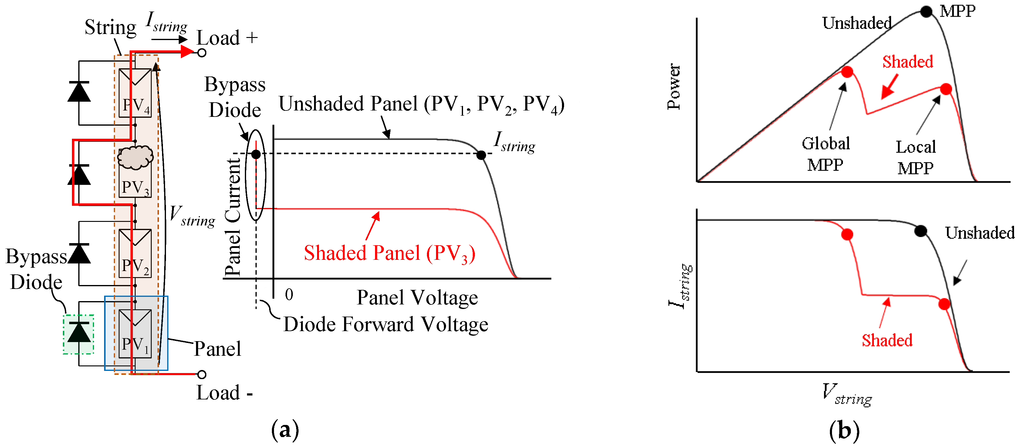
:1. Introduction
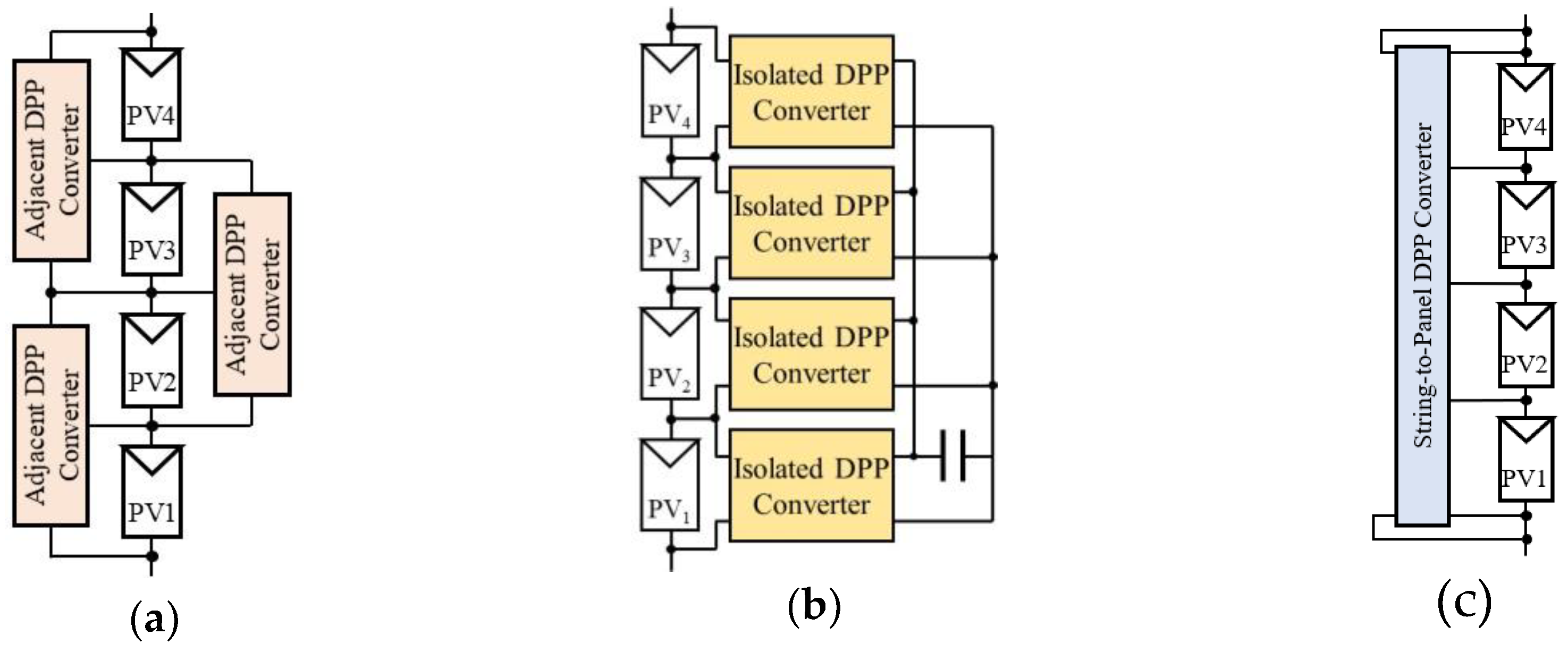
2. Proposed DPP Converter Based on Voltage Divider and LLC Resonant Voltage Multiplier
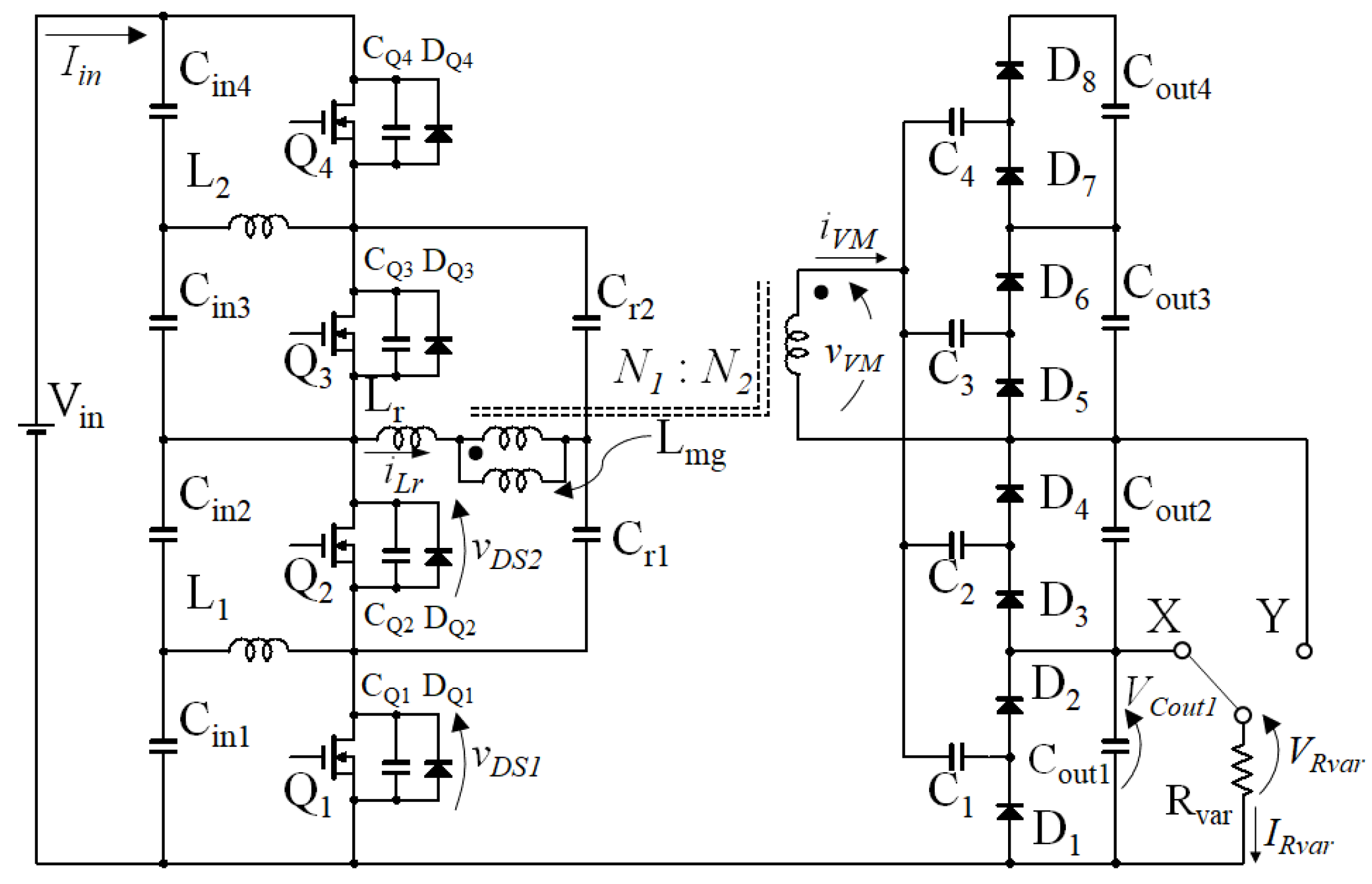
2.1. Key Circuits for Proposed DPP Converter
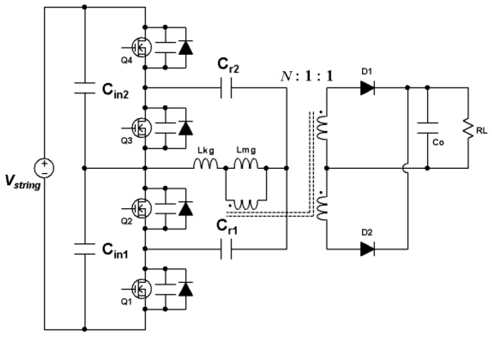
2.2. Proposed DPP Converter
2.3. Major Features
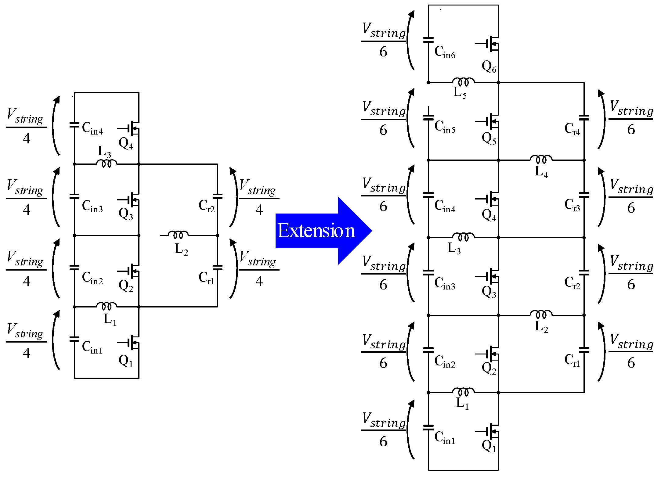
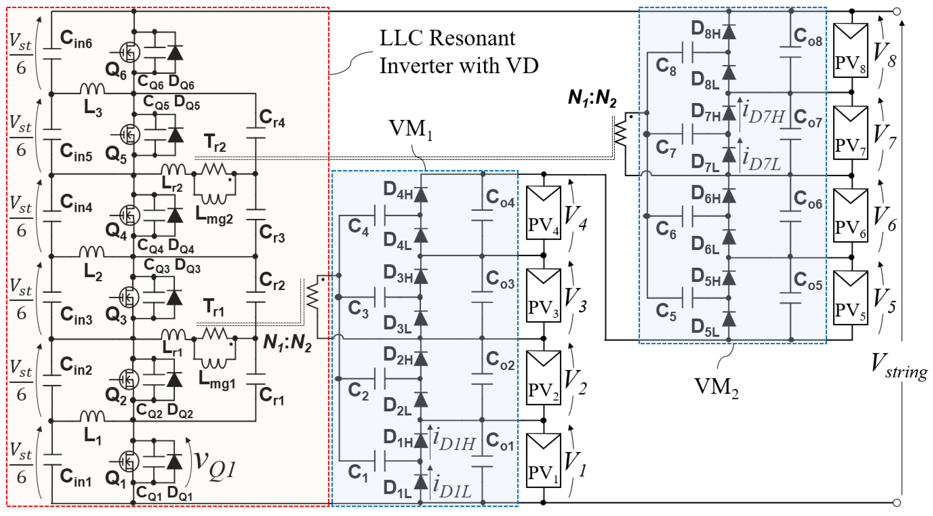
2.4. Extended Topology of Proposed DPP Converter
3. Operation Analysis
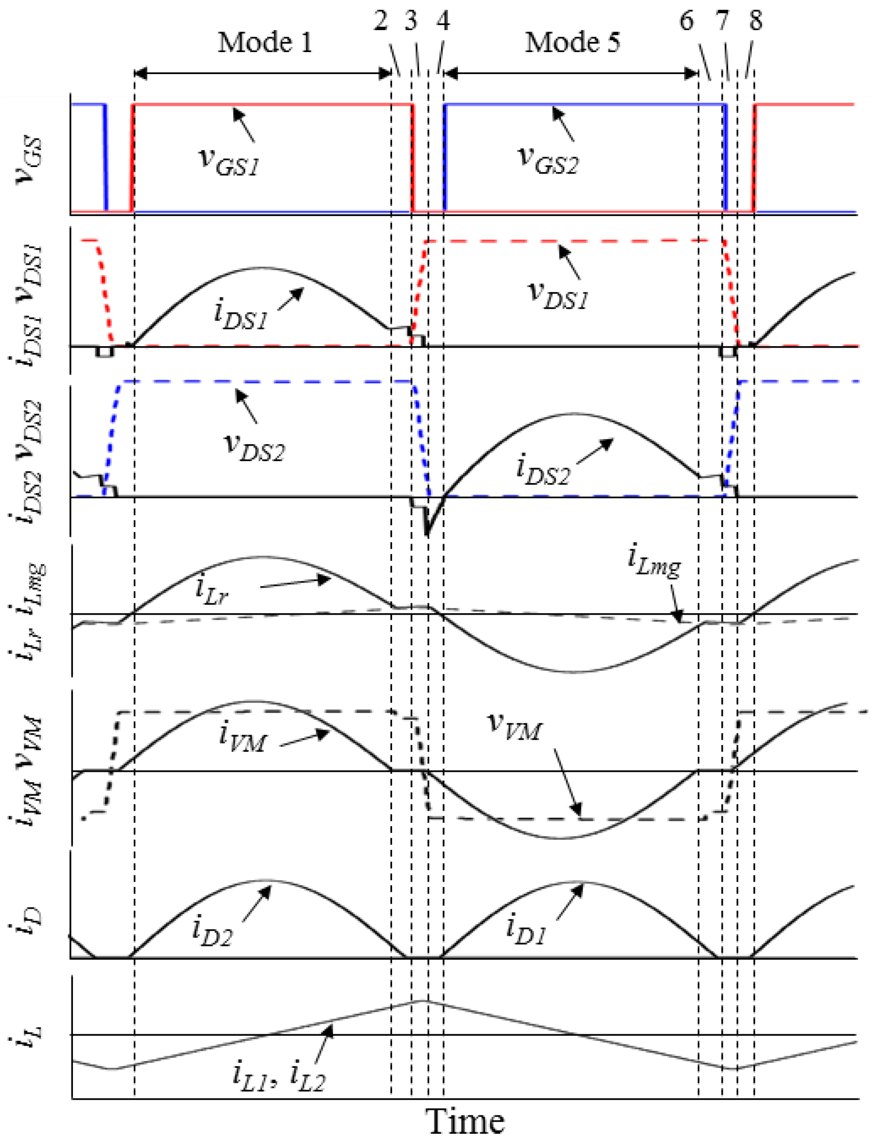
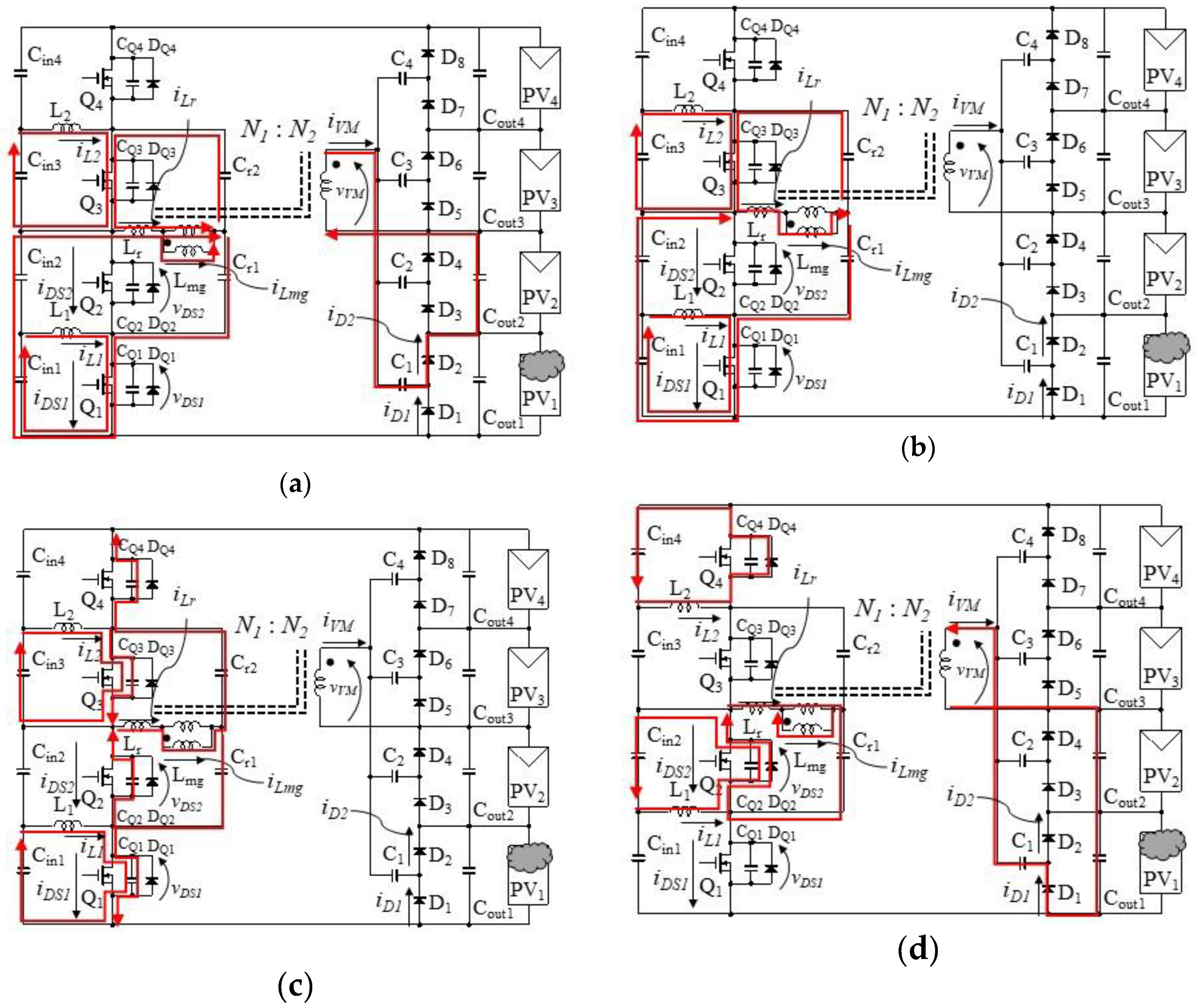
3.1. Operation Principle
3.2. Operation Boundary
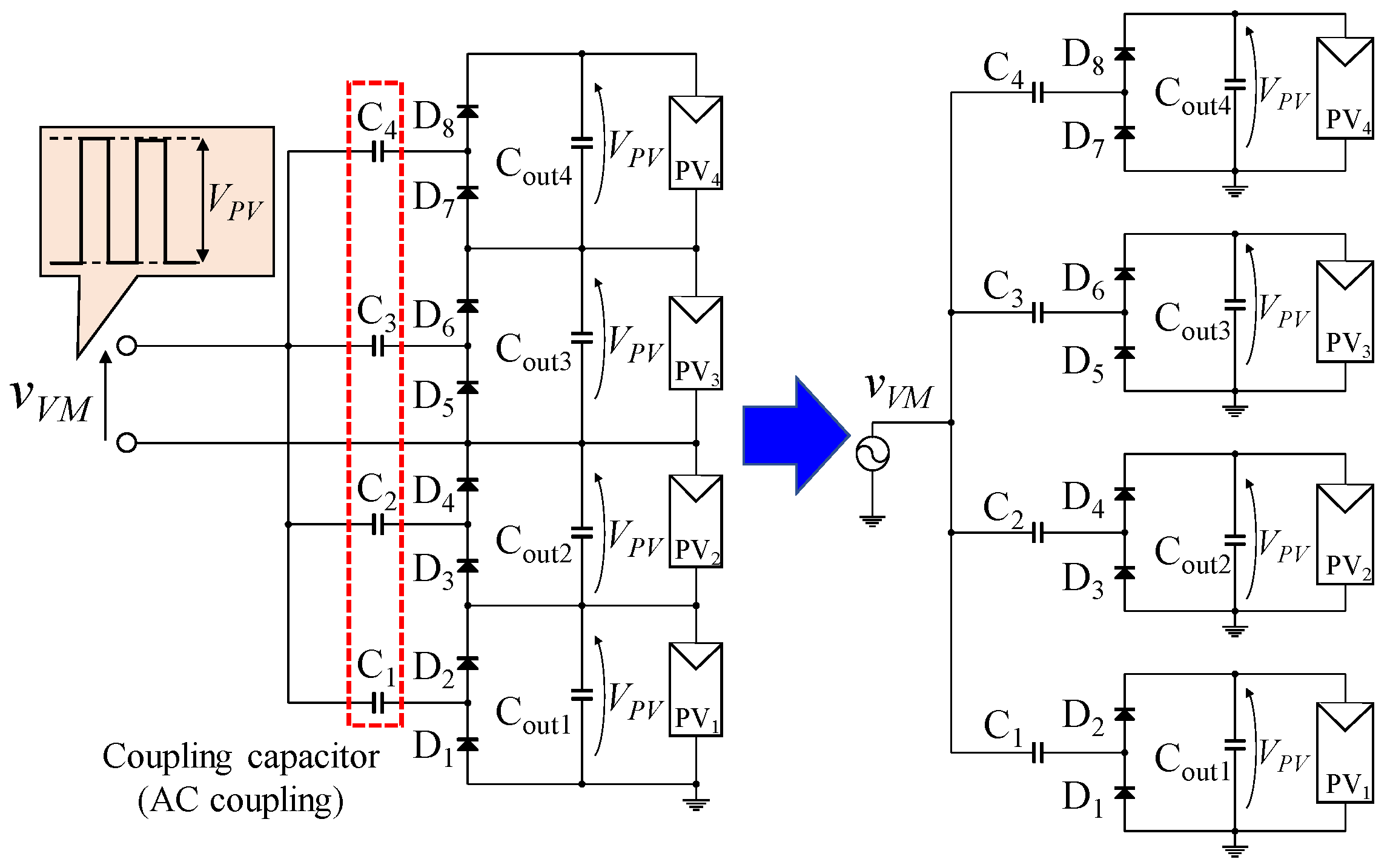
3.3. Voltage Equalization Mechanism of Voltage Multiplier
3.4. Design Guideline for LLC Resonant Inverter
3.5. Peak Current of Inductor
4. Experimental Results
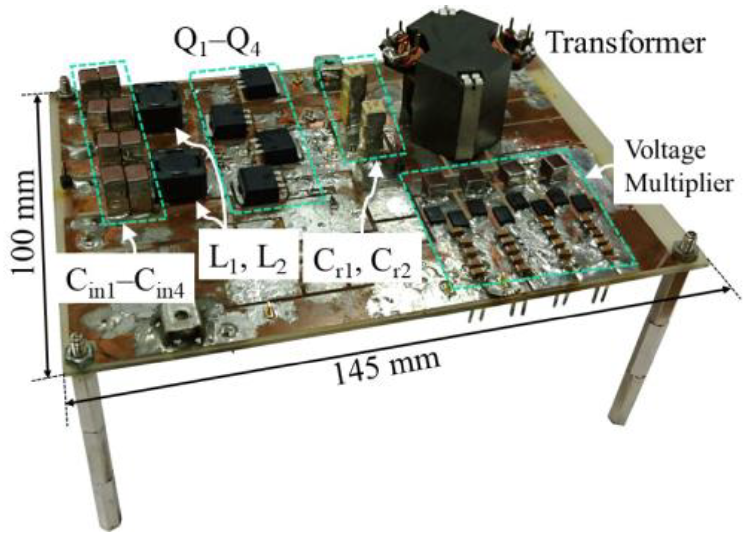
4.1. Prototype
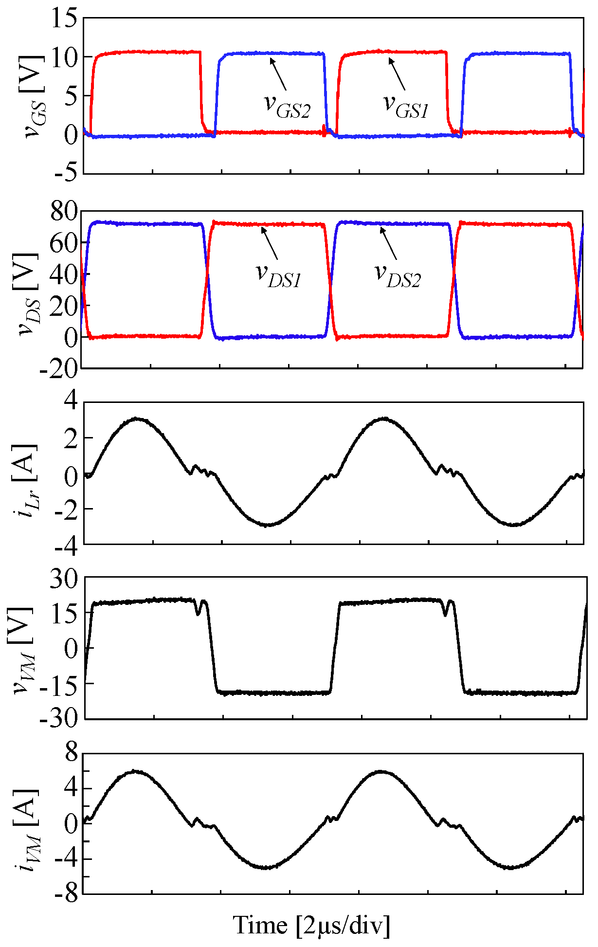
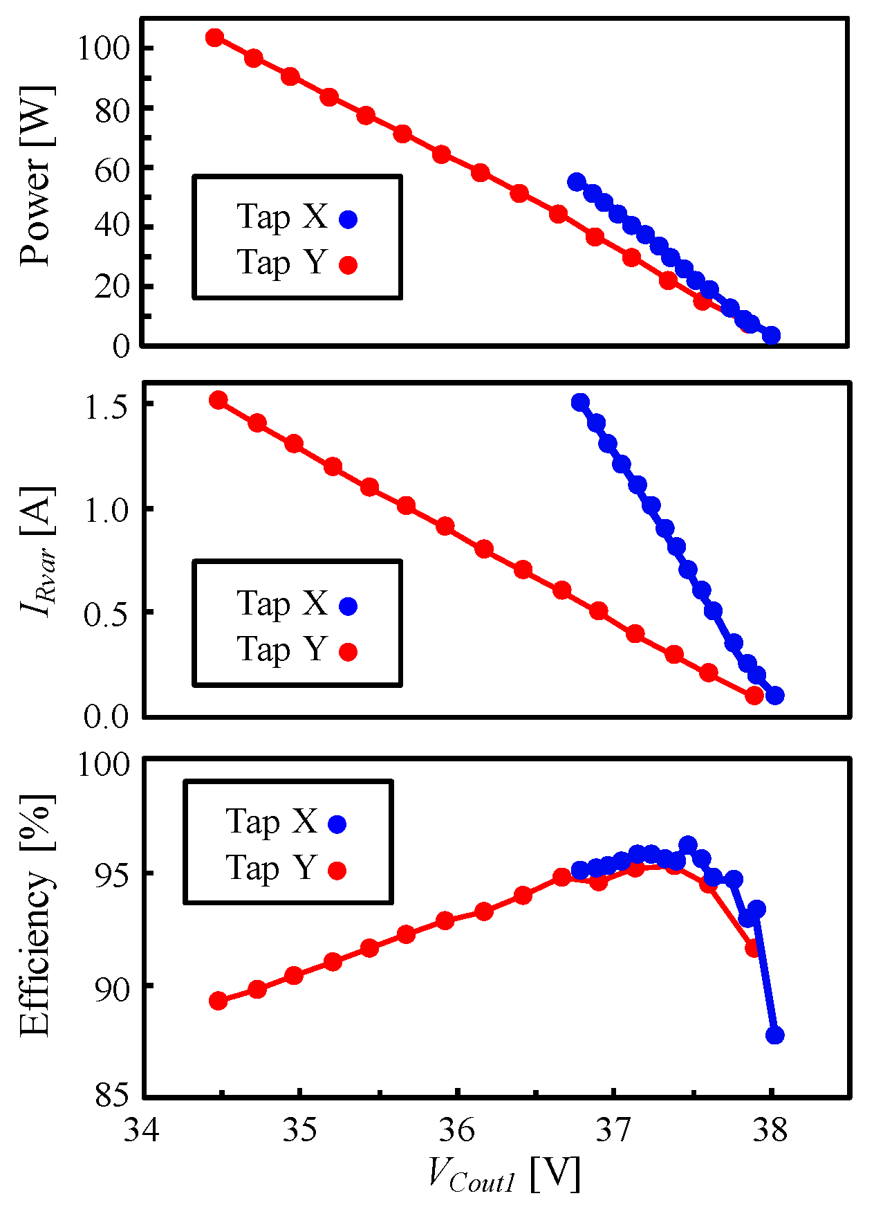
4.2. Fundamental Characteristics of DPP Converter
4.3. Equalization Test in Laboratory
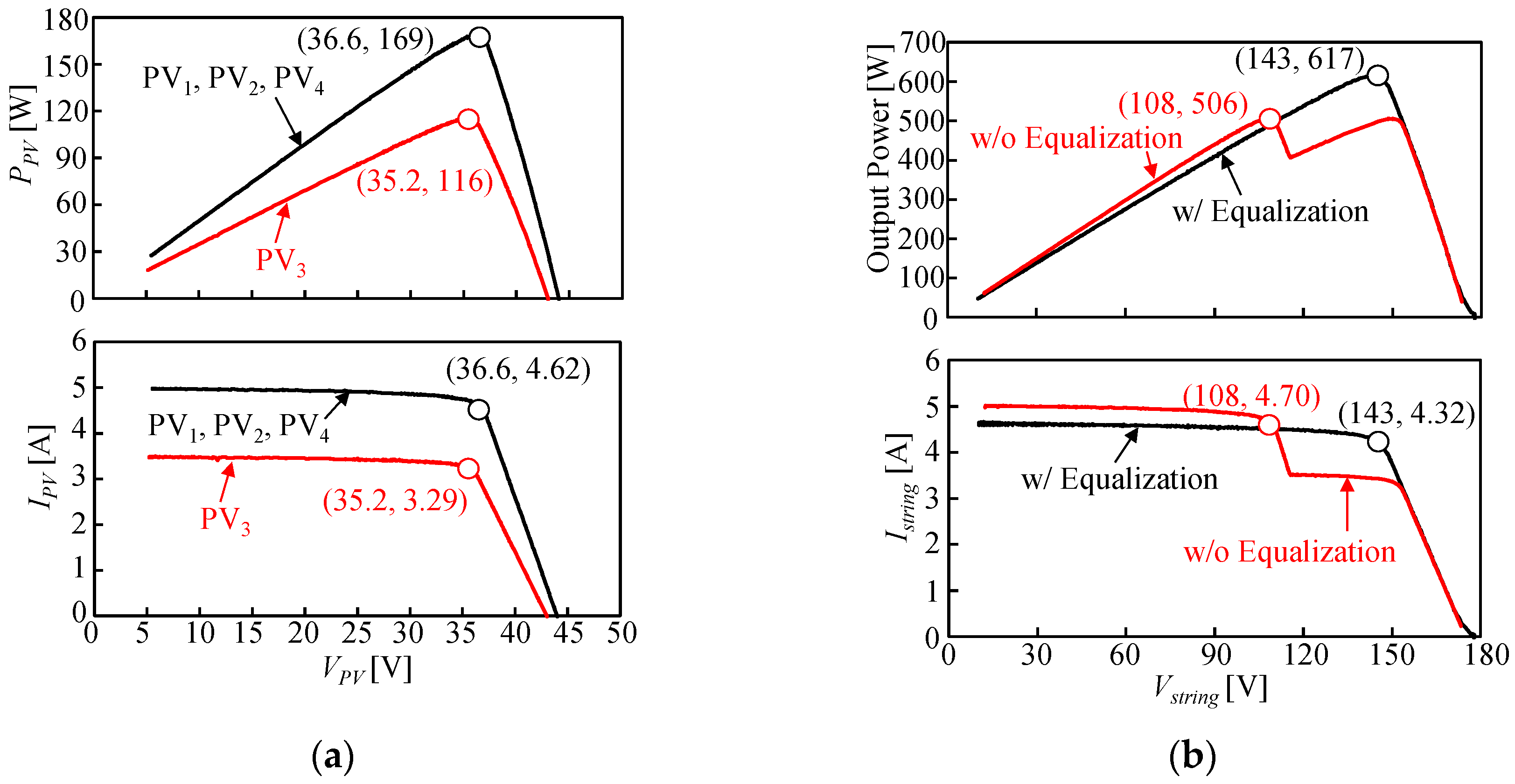
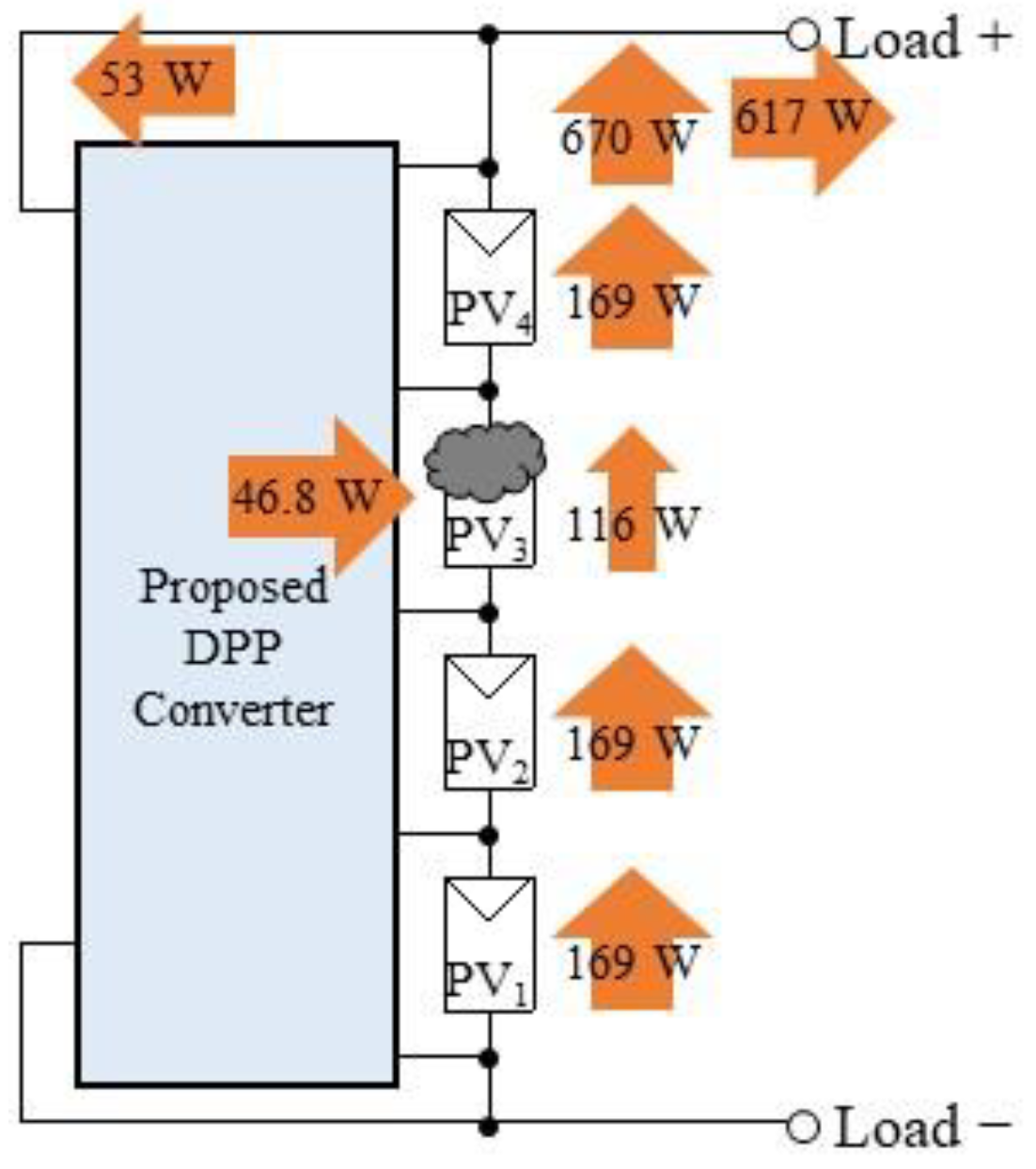
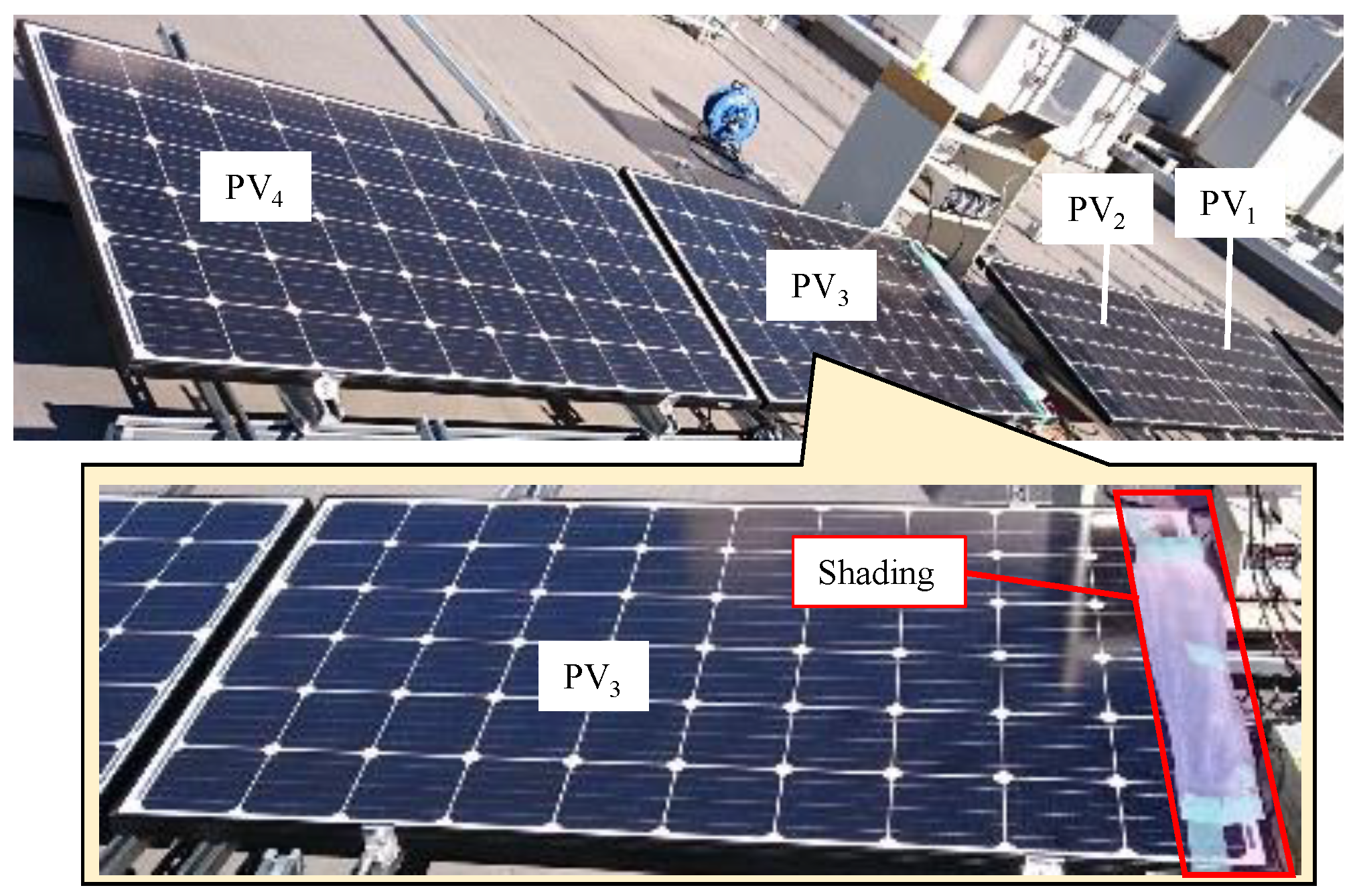
4.4. Field Testing
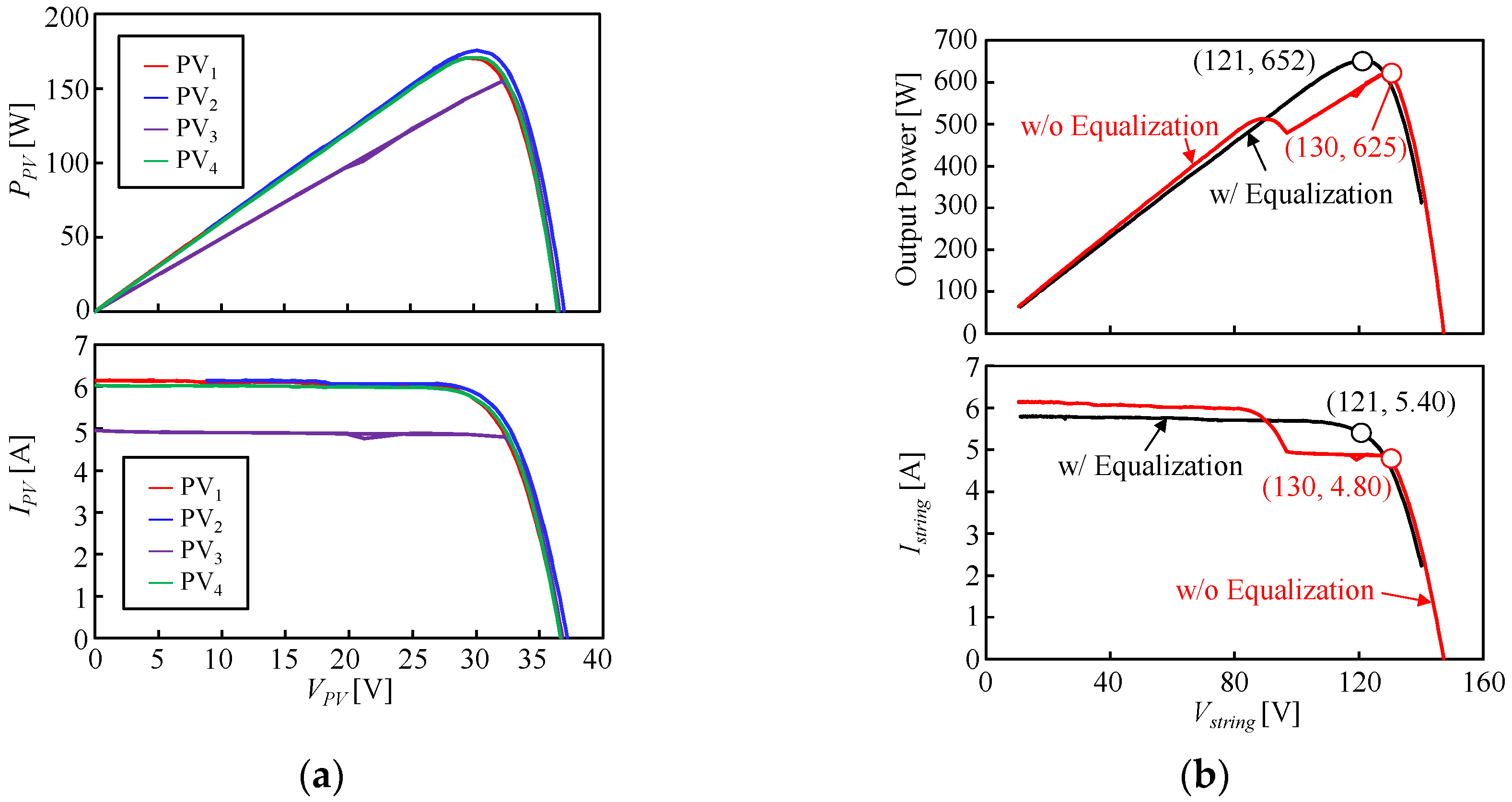
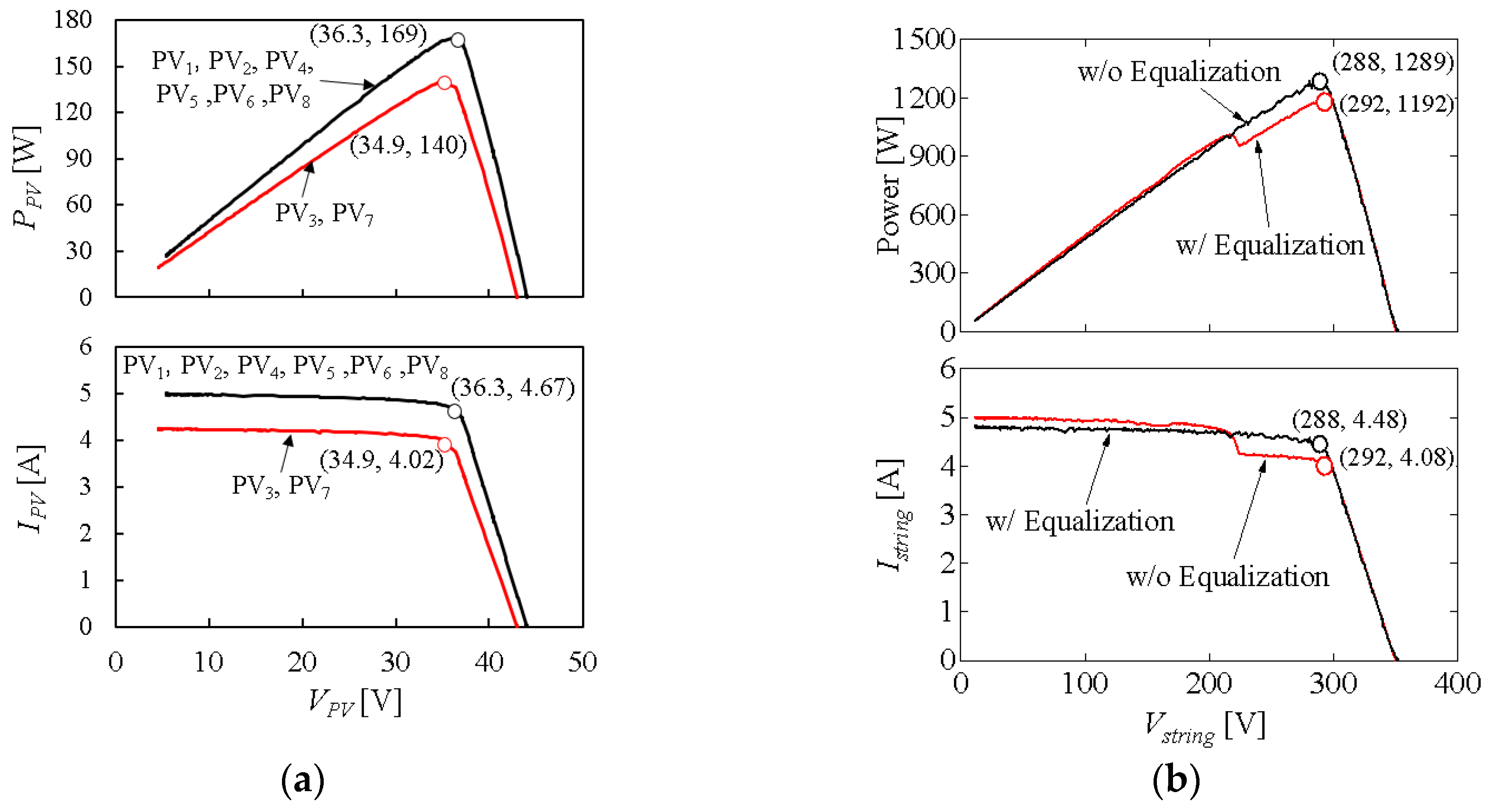
4.5. Extended DPP Converter for Eight Panels Connected in Series
5. Conclusions
Author Contributions
Funding
Conflicts of Interest
References
- MacAlpine, S.M.; Erickson, R.W.; Brandemuehl, M.J. Characterization of power optimizer potential to increase energy capture in photovoltaic systems operating under nonuniform conditions. IEEE Trans. Power Electron. 2013, 28, 2936–2945. [Google Scholar] [CrossRef]
- Ramli, M.A.M.; Twaha, S.; Ishaque, K.; Turki, Y.A.A. A review on maximum power point tracking for photovoltaic systems with and without shading conditions. Renew. Sustain. Energy Rev. 2017, 67, 144–159. [Google Scholar] [CrossRef]
- Qin, S.; Cady, S.T.; García, A.D.D.; Podgurski, R.C.N.P. A distributed approach to maximum power point tracking for photovoltaic submodule differential power processing. IEEE Trans. Power Electron. 2015, 30, 2024–2040. [Google Scholar] [CrossRef]
- Qin, S.; Barth, C.B.; Podgurski, R.C.N.P. Enhancing microinverter energy capture with submodule differential power processing. IEEE Trans. Power Electron. 2016, 31, 3575–3585. [Google Scholar] [CrossRef]
- Bergveld, H.J.; Büthker, D.; Castello, C.; Doorn, T.; Jong, A.D.; Otten, R.V.; Waal, K.D. Module-level dc/dc conversion for photovoltaic systems: The delta-conversion concept. IEEE Trans. Power Electron. 2013, 28, 2005–2013. [Google Scholar] [CrossRef]
- Shenoy, P.S.; Kim, K.A.; Johnson, B.B.; Krein, P.T. Differential power processing for increased energy production and reliability of photovoltaic systems. IEEE Trans. Ind. Power Electron. 2013, 28, 2968–2979. [Google Scholar] [CrossRef]
- Shimizu, T.; Hirakata, M.; Kamezawa, T.; Watanabe, H. Generation control circuit for photovoltaic modules. IEEE Trans. Power Electron. 2001, 16, 293–300. [Google Scholar] [CrossRef]
- Shimizu, T.; Hashimoto, O.; Kimura, G. A novel high-performance utility-interactive photovoltaic inverter system. IEEE Trans. Power Electron. 2003, 18, 704–711. [Google Scholar] [CrossRef] [Green Version]
- Wang, F.; Zhu, T.; Zhuo, F.; Yi, H. An improved submodule differential power processing-based PV system with flexible multi-MPPT control. IEEE J. Emerg. Sel. Top. 2018, 6, 94–102. [Google Scholar] [CrossRef]
- Ramli, M.Z.; Salam, Z. A simple energy recovery scheme to harvest the energy from shaded photovoltaic modules during partial shading. IEEE Tran. Power Electron. 2014, 29, 6458–6471. [Google Scholar] [CrossRef]
- Blumenfeld, A.; Cervera, A.; Peretz, M.M. Enhanced differential power processor for PV systems: Resonant switched-capacitor gyrator converter with local MPPT. IEEE J. Emerg. Sel. Top. Power Electron. 2014, 2, 883–892. [Google Scholar] [CrossRef]
- Gokdaga, M.; Akbabab, M.; Gulbudakc, O. Switched-capacitor converter for PV modules under partial shading and mismatch conditions. Sol. Energy 2018, 170, 723–731. [Google Scholar] [CrossRef]
- Uno, M.; Kukita, A. PWM converter integrating switched capacitor converter and series-resonant voltage multiplier as equalizers for photovoltaic modules and series-connected energy storage cells for exploration rovers. IEEE Trans. Power Electron. 2017, 32, 8500–8513. [Google Scholar] [CrossRef]
- Stauth, J.T.; Seeman, M.D.; Kesarwani, K. Resonant switched-capacitor converters for sub-module distributed photovoltaic power management. IEEE Trans. Power Electron. 2013, 28, 1189–1198. [Google Scholar] [CrossRef]
- Chang, A.H.; Avestruz, A.T.; Leeb, S.B. Capacitor-less photovoltaic cell-level power balancing using diffusion charge redistribution. IEEE Trans. Power Electron. 2015, 30, 537–546. [Google Scholar] [CrossRef]
- Uno, M.; Saito, Y.; Yamamoto, M.; Urabe, S. PWM switched capacitor-based cell-level power balancing converter utilizing diffusion capacitance of photovoltaic cells. IEEE Trans. Power Electron. 2019, 34, 10675–10687. [Google Scholar] [CrossRef]
- Uno, M.; Yamamoto, M.; Sato, H.; Oyama, S. Modularized differential power processing architecture based on switched capacitor converter to virtually unify mismatched photovoltaic panel characteristics. IEEE Trans. Power Electron. 2019, in press. [Google Scholar] [CrossRef]
- Olalla, C.; Clement, D.; Rodríguez, M.; Makisimović, D. Architectures and control of submodule integrated dc-dc converters for photovoltaic applications. IEEE Trans. Power Electron. 2013, 28, 2980–2997. [Google Scholar] [CrossRef]
- Levron, Y.; Clement, D.R.; Choi, B.; Olalla, C.; Maksimovic, D. Control of submodule integrated converters in the isolated-port differential power-processing photovoltaic architecture. IEEE J. Emerg. Sel. Top. Power Electron. 2014, 2, 821–832. [Google Scholar] [CrossRef]
- Bell, R.; Podgurski, R.C.N.P. Decoupled and distributed maximum power point tracking of series-connected photovoltaic submodules using differential power processing. IEEE J. Emerg. Sel. Top. Power Electron. 2015, 3, 881–891. [Google Scholar] [CrossRef]
- Olalla, C.; Deline, C.; Clement, D.; Levron, Y.; Rodríguez, M.; Makisimović, D. Performance of power limited differential power processing architectures in mismatched PV systems. IEEE Trans. Power Electron. 2015, 30, 618–631. [Google Scholar] [CrossRef]
- Chu, G.; Wen, H.; Jiang, L.; Hu, Y.; Li, X. Bidirectional flyback based isolated-port submodule differential power processing optimizer for photovoltaic applications. Sol. Energy 2017, 158, 929–940. [Google Scholar] [CrossRef] [Green Version]
- Jeon, Y.T.; Lee, H.; Kim, K.A.; Park, J.H. Least power point tracking method for photovoltaic differential power processing systems. IEEE Trans. Power Electron. 2017, 32, 1941–1951. [Google Scholar] [CrossRef]
- Jeon, Y.T.; Park, J.H. Unit-minimum least power point tracking for the optimization of photovoltaic differential power processing systems. IEEE Trans. Power Electron. 2019, 34, 311–324. [Google Scholar] [CrossRef]
- Du, J.; Xu, R.; Chen, X.; Li, Y.; Wu, J. A novel solar panel optimizer with self-compensation for partial shadow condition. In Proceedings of the IEEE Applied Power Electron. Conference and Exposition (APEC), Long Beach, CA, USA, 17–21 March 2013; pp. 92–96. [Google Scholar]
- Uno, M.; Kukita, A. Single-switch voltage equalizer using multi-stacked buck–boost converters for partially-shaded photovoltaic modules. IEEE Trans. Power Electron. 2015, 30, 3091–3105. [Google Scholar] [CrossRef]
- Uno, M.; Kukita, A. Current sensorless equalization strategy for a single-switch voltage equalizer using multistacked buck–boost converters for photovoltaic modules under partial shading. IEEE Trans. Ind. Appl. 2017, 53, 420–429. [Google Scholar] [CrossRef]
- Uno, M.; Kukita, A. Two-switch voltage equalizer using an LLC resonant inverter and voltage multiplier for partially shaded series connected photovoltaics modules. IEEE Trans. Ind. Appl. 2015, 51, 1587–1601. [Google Scholar] [CrossRef]
- Uno, M.; Kukita, A. Single-switch single-magnetic PWM converter integrating voltage equalizer for partially-shaded photovoltaic modules in standalone applications. IEEE Trans. Power Electron. 2018, 33, 1259–1270. [Google Scholar] [CrossRef]
- Uno, M.; Shinohara, T. Variable switching frequency modulation scheme for PWM converter integrating series-resonant voltage multiplier-based voltage equalizer for photovoltaic strings under partial shading. IEEJ Trans. Electr. Electron. Eng. 2019, 14, 467–474. [Google Scholar] [CrossRef]
- Uno, M.; Shinohara, T.; Saito, Y.; Kukita, A. Review, comparison, and proposal for PWM converters integrating differential power processing converter for small exploration rovers. Energies 2019, 12, 1919. [Google Scholar] [CrossRef]
- Ruan, X.; Li, B.; Chen, Q.; Tan, S.C.; Tse, C.K. Fundamental considerations of three-level DC–DC converters: Topologies, analyses, and control. IEEE Trans. Power Electron. 2008, 55, 3733–3743. [Google Scholar]
- Lee, I.O.; Moon, G.W. Analysis and design of a three-level LLC series resonant converter for high- and wide-input-voltage applications. IEEE Trans. Power Electron. 2012, 27, 2966–2979. [Google Scholar] [CrossRef]
- Choi, H. Design Consideration for an LLC-Resonant Converter. Proceedings of the Fairchild Power Seminar. 2007, pp. A1–A9. Available online: http://citeseerx.ist.psu.edu/viewdoc/download?doi=10.1.1.397.2440&rep=rep1&type=pdf (accessed on 19 October 2019).
- Kim, K.A.; Shenoy, P.S.; Krein, P.T. Converter rating analysis for photovoltaic differential power processing systems. IEEE Trans. Ind. Electron. 2015, 30, 1987–1997. [Google Scholar] [CrossRef]
- Olalla, C.; Hasan, M.N.; Deline, C.; Maksimovi, D. Mitigation of hot-spots in photovoltaic systems using distributed power electronics. Energies 2018, 11, 726. [Google Scholar] [CrossRef]


| Component | Value |
|---|---|
| Q1–Q4 | IRF644PSBF, VDS = 250 V, Ron = 0.28 Ω, CQ = 330 pF |
| Cin1–Cin4 | MLCC, 40 μF (= 10 μF × 4), 100 V |
| Cr1, Cr2 | Film Capacitor, 400 nF (= 100 nF × 4), 100 V |
| L1, L2 | 470 μH |
| C1–C4 | MLCC, 20 μF (= 10 μF × 2), 100 V |
| Cout1–Cout4 | MLCC, 50 μF (= 10 μF × 5), 50 V |
| D1–D8 | Schottky Diode, SBRT20M60SP5, VD = 0.57 V |
| Transformer | N1:N2 = 13:7, Lr = 1.18 μH, Lmg = 175 μH, RTp = 1.77 Ω, RTs = 1.77 Ω |
© 2019 by the authors. Licensee MDPI, Basel, Switzerland. This article is an open access article distributed under the terms and conditions of the Creative Commons Attribution (CC BY) license (http://creativecommons.org/licenses/by/4.0/).
Share and Cite
Uno, M.; Nakane, T.; Shinohara, T. LLC Resonant Voltage Multiplier-Based Differential Power Processing Converter Using Voltage Divider with Reduced Voltage Stress for Series-Connected Photovoltaic Panels under Partial Shading. Electronics 2019, 8, 1193. https://0-doi-org.brum.beds.ac.uk/10.3390/electronics8101193
Uno M, Nakane T, Shinohara T. LLC Resonant Voltage Multiplier-Based Differential Power Processing Converter Using Voltage Divider with Reduced Voltage Stress for Series-Connected Photovoltaic Panels under Partial Shading. Electronics. 2019; 8(10):1193. https://0-doi-org.brum.beds.ac.uk/10.3390/electronics8101193
Chicago/Turabian StyleUno, Masatoshi, Toru Nakane, and Toshiki Shinohara. 2019. "LLC Resonant Voltage Multiplier-Based Differential Power Processing Converter Using Voltage Divider with Reduced Voltage Stress for Series-Connected Photovoltaic Panels under Partial Shading" Electronics 8, no. 10: 1193. https://0-doi-org.brum.beds.ac.uk/10.3390/electronics8101193