An Efficient Hybrid Filter-Based Phase-Locked Loop under Adverse Grid Conditions

1
School of Information Science & Engineering, Northeastern University, Shenyang 110819, Liaoning, China
2
School of Electrical Engineering, Shenyang University of Technology, Shenyang 110870, Liaoning, China
*
Author to whom correspondence should be addressed.
Energies 2018, 11(4), 703; https://0-doi-org.brum.beds.ac.uk/10.3390/en11040703
Submission received: 25 February 2018
/
Revised: 19 March 2018
/
Accepted: 19 March 2018
/
Published: 21 March 2018
(This article belongs to the Special Issue Emerging Power Electronics Technologies for Power Systems and Machine Drives)
Abstract
:Synchronous-reference-frame phase-locked loop (SRF-PLL) is widely used in grid synchronization applications. However, under unbalanced, distorted and DC offset mixed grid conditions, its performance tends to worsen. In order to improve the filtering capability of SRF-PLL, a modified three-order generalized integrator (MTOGI) with DC offset rejection capability based on conventional three order generalized integrator (TOGI) and an enhanced delayed signal cancellation (EDSC) are proposed, then dual modified TOGI (DMTOGI) filtering stage is designed and incorporated into the SRF-PLL control loop with EDSC to form a new hybrid filter-based PLL. The proposed PLL can reject the fundamental frequency negative sequence (FFNS) component, DC offset component, and the rest of harmonic components in SRF-PLL input three-phase voltages at the same time with a simple complexity. The proposed PLL in this paper has a faster transient response due to the EDSC reducing the number of DSC operators. A small-signal model of the proposed PLL is derived. The stability is analyzed and parameter design guidelines are given. Experimental results are included to validate the effectiveness and robustness of the proposed PLL.
1. Introduction
The accurate estimation of grid voltage phase is the key technology in the control of the three-phase grid-connected power converter. With the continuous innovation and development of new energy power generation technologies such as solar energy and wind energy, the operation of the grid becomes more and more complicated. Imbalances and frequency fluctuations in the grid voltage are caused by sudden failure in the grid and sudden change of grid load [1,2]. Thus, to achieve a quick and accurate of estimation of grid voltage phase under adverse grid conditions such as grid voltage imbalance and distortion is an issue of focus in the field of new energy grid-connections [3,4].
To deal with phase estimation problem under non-ideal grid voltage, many PLL methods have been proposed by scholars. Most of these methods are based on the synchronous reference frame PLL (SRF-PLL). The conventional SRF-PLL has excellent phase tracking capability and dynamic performance under ideal grid conditions. However, when the grid voltage is unbalanced and distorted, an oscillation will be introduced into the phase estimation [5,6].
To eliminate the effect of fundamental frequency negative sequence (FFNS) component and harmonic components under unbalanced and distorted grid conditions, a variety of advanced PLLs have been proposed such as dual second-order generalized integrator PLL (DSOGI-PLL), dual three-order generalized integrator PLL (DTOGI-PLL), and multi-complex-coefficient filter PLL (MCCF-PLL). Reference [7] proposed a grid-connected synchronization method based on a second-order generalized integrator. First, the second-order generalized integrator generated the quadrature signal, then the symmetrical component approach was used to calculate the positive and negative sequence voltage components. This approach does not require reference frames rotating and is more simple to implement than the DTOGI-PLL and MCCF-PLL, but synchronization errors are greater in the case of grid voltage with harmonic distortion. Reference [8] proposed a DTOGI-PLL that uses two third-order generalized integrator bandpass filters instead of the SOGI structure in DSOGI-PLL. The DTOGI-PLL has a better inherent filtering characteristic than the DSOGI-PLL by using a complex transfer function with high-order denominator. In reference [9], the fundamental frequency positive sequence (FFPS) and FFNS components are separated using the amplitude-frequency and phase-frequency asymmetric characteristic of complex-coefficient filter (CCF), and specific order harmonics are selectively eliminated or extracted by multiple CCFs in parallel. The main problem of the above PLLs is that they only mitigate but do not completely eliminate influence of all the major harmonic components. In order to completely reject all the dominant harmonics without degrading the dynamic performance, some scholars have used some linear filtering techniques in SRF-PLL, such as delayed signal cancellation operator [10,11]. The DSC-PLL is widely used in grid-connected synchronization technology under distorted grids due to its easy digital implementation and excellent filtering capability. Most of the DSC-based PLLs cascade multiple DSCs to improve the filtering performance whether in the phase control loop of the PLL or before the input of the PLL [12]. The number of DSCs depends on eliminated the harmonic components. Reference [13] proposed a generalized DSC structure cascading five DSC operators with delay factors n = 2; 4; 8; 16; 32 (which is briefly called the GDSC 2, 4, 8, 16, 32), and combined it into the control outer loop of the conventional SRF-PLL. The delay caused by the DSCs structure is the sum of multiple DSC delays, therefore, the dynamic response of the system will be significantly degraded. Reference [14] proposed a frequency adaptive generalized DSC (GDSC) operator, but its structural nonlinearity is so high that it is difficult to ensure the stability of the entire system. In reference [15], an efficient GDSC (EGDSC) is proposed based on the non-frequency adaptive GDSC structure with additional frequency and phase error compensation units, which increases the system stability and reduces the computational complexity.
In addition, another problem in designing PLL is the existence of DC offsets in the input voltage which can cause fundamental frequency oscillation errors in the phase and frequency estimates of PLL [16,17,18,19,20]. In order to eliminate the phase and frequency estimation error caused by DC offset, reference [21] proposed a SO-SOGI-QSG filter consisting of two cascaded SOGI filter units, this method can completely remove the components of −50 Hz in the dq-frame and effectively eliminate the influence of DC offset. Reference [22] proposed a frequency-adaptive filtering MAF unit in stationary frame system to obtain and eliminate constant DC offset components. However, in reference [23], a modified MAF filtering unit was used to quickly eliminate constant and slow speed changing DC offset components within 1 ms. These methods can effectively eliminate the effects of DC offset, but increase the system response time and additional computational burden.
This paper proposes a modified TOGI (MTOGI) structure that based on the conventional TOGI to block DC offset components completely, and also provides an enhanced DSC (EDSC) operator based on modified DSC approach to eliminate harmonic components. Then a dual modified TOGI (DMTOGI) filter stage is designed. The DMTOGI is transformed to the dq-frame and cascaded with EDSC to form a new hybrid filter which is incorporated into the SRF-PLL control inner loop. The hybrid filter can be employed to eliminate the FFNS component, the DC offset components and all harmonic components of the SRF-PLL input three-phase grid voltage. Because the EDSC can reduce the number of DSC operators and improve the transient response of the system, so the proposed PLL can extract the grid voltage synchronization signal quickly and accurately when the grid voltage is unbalanced and severely distorted. The effectiveness of the proposed PLL under non-ideal grid voltages is confirmed through experimental results.
2. PLL Input Voltage Component Analysis
Assuming that the PLL three-phase input voltages are under adverse conditions, it means that the voltage contains the fundamental voltage component, the DC offset component, and each harmonic component. The three-phase input voltage after Fourier transform can be expressed as
where k = a,b,c, U0k is the DC offset component, U1k is the amplitude of the fundamental voltage, Unk is the amplitude of the n-th harmonic component; θk1 is the phase angle of the fundamental component; θkn is the phase angle of n-th harmonic component.
In PLLs, the three-phase voltages even harmonics are eliminated in the αβ-frame after the Clark transformation. 3nth harmonics are decoupled and centered on the 0 axis. So three-phase voltage in the αβ-frame only contain +1th, −5th, +7th, −11th, +13th, … voltage components [24]. The DC offset component in the αβ-frame still behaves as a DC voltage component, which is on the 0 axis. Under unbalanced grid conditions, the fundamental negative-sequence component appears as −1th voltage component in the αβ-frame.
When the voltage signal is transformed to the dq-frame after Park transformation, the frequency of each harmonic voltage component is changed. The dq-frame can be obtained by rotating the αβ-frame at a speed of 2π50 rad/s counterclockwise, and then the +1th, −5th, +7th, −11th, +13th, … voltage components in αβ-frame are shown as 0th, −2th, ±6th, ±12th, … voltage components in dq-frame [25]. The DC offset component behaves as a −1th voltage component.
Table 1 summarizes the above conclusions and provides the dominant components of the grid voltage. As shown in Table 1, some frequency components are negative, which means that the voltage components of the grid are negative sequence voltage. It can be observed that the FFNS component and the DC offset component in the αβ-frame are voltage components at −50 Hz and 0 Hz, which are presented as voltage components at −100 Hz and −50 Hz in the dq-frame. Therefore, blocking FFNS, DC offset and all harmonic components in SRF-PLL inner loop means to eliminate voltage components at −50 Hz, −100 Hz, ±300 Hz, ±600 Hz, … in dq-frame.
3. DMTOGI Design Based on Complex Vector Filter
This section proposes a MTOGI filter unit with DC offset rejection capability and constructs and designs the DMTOGI filter using the complex vector filter approach.
3.1. Complex Vector Filter Overview
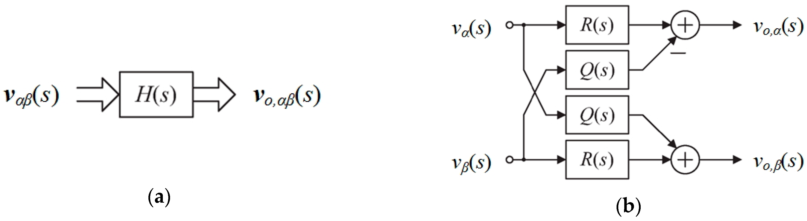
The Clark transformation is actually the process of converting three independent quantities of the three-phase grid voltage or current into one rotating vector. This rotating vector in the αβ frame system can be expressed as follow in the s domain.
where, vα(s) is the α-axis real domain expression which denotes the real part of the voltage vector and vβ(s) is the β-axis real domain expression which denotes the imaginary part of the voltage vector.
Referencing the complex domain vector representation of the grid voltage, the concept of a complex vector filter can be introduced. The complex vector filter is actually a double-input dual-output complex transfer function. The complex vector filter is shown in Figure 1, where H(s) is the transfer function of the complex vector filter with the following expression [26]
where R(s) is the real part of the transfer function and Q(s) is the imaginary part of the transfer function.
According to Figure 1, Equations (2) and (3), we can obtain the output of the complex vector filter vo,αβ(s)
where
The implementation of the complex vector filter based on the real domain transfer function is shown in Figure 1b.
It can be seen from Equation (4) that when a complex domain vector and complex filter multiplied, it can be understood as the multiplication of two vectors. The amplitude–frequency characteristic and phase–frequency characteristic of the complex vector filter can be obtained by substituting s = jω into H(s).
3.2. Design of MTOGI
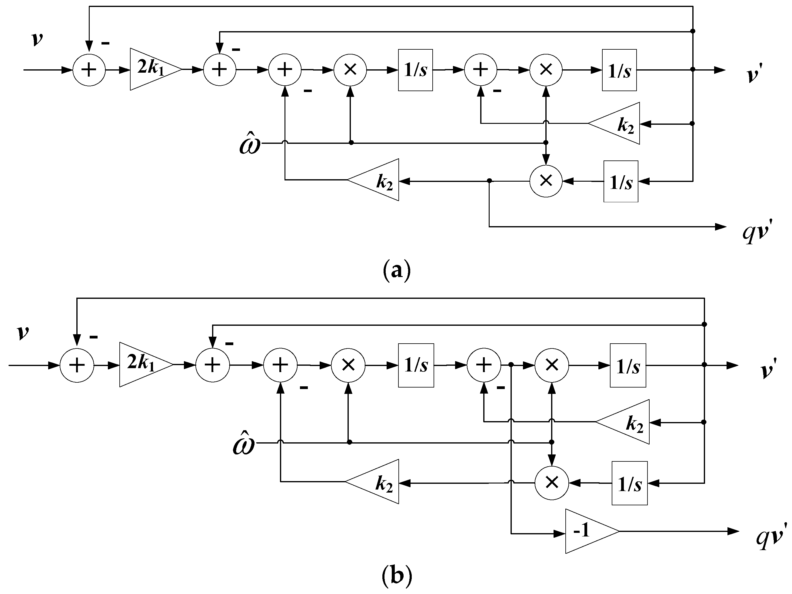
The conventional TOGI structure in reference [8] is shown in Figure 2a, which has one input and two outputs. The two outputs are the direct axis component and quadrature axis of the filtered signal. The transfer function of conventional TOGI is
where v is the input signal of TOGI, q is the phase shift factor with 90°, is the estimate value of the grid voltage frequency, v′ and qv′ are the direct and quadrature versions of the input signal v, respectively, k1 and k2 are dynamic coefficients. It can be observed that Rc(s) has a zero at s = 0, so the DC offset can be completely rejected. However, the output of v′ does not contain the DC offset component. From the structure Figure 2a, v′ eliminates the DC component by inverse feedback to the input signal. As shown in Figure 2a, since Qc(s) is a low-pass filter, once the input signal v contains any DC component, the output signal qv′ will be affected by DC offset, which causes the amplitude detection error of the input voltage signal and affects the following phase angle lock.
To reject the DC offset completely, as shown in Figure 2b, the same structure as the conventional TOGI is employed in this paper, but the quadrature signal qv′ is taken from different points to construct a modified TOGI(MTOGI). The modified TOGI transfer function is
The transfer function of Rm(s) is same as Rc(s), and the transfer function of Qm(s) is changed. There is zero at s = 0 in Qm(s), it means that there is zero at 0 Hz, and the DC component in the quadrature axis signal (qv′) can be rejected completely.
3.3. DMTOGI Filter Structure
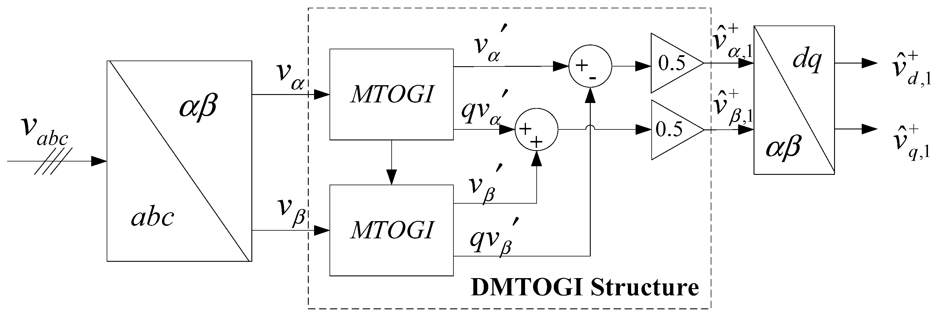
In this paper, two TOGIs in DTOGI filter stage are replaced with MTOGI in Figure 2b, and a dual modified TOGI (DMTOGI) filter is proposed. The modified filtering stage can reject grid voltage FFNS component and DC Offset without increasing calculation burden.
Figure 3 shows the DMTOGI structure, and the expression of Figure 3 is written as
where vα, vβ are the voltage signal in αβ-frame after Clark transformation to the three-phase voltage vabc. and , which only contain voltage positive sequence component, are the output after vα′ and vβ′ undergoing the interleaved positive sequence components calculation. According to the complex vector filter Equations (4) and (11), the DMTOGI filter in the αβ frame (called αβDMTOGI) can be written as a complex vector transfer function
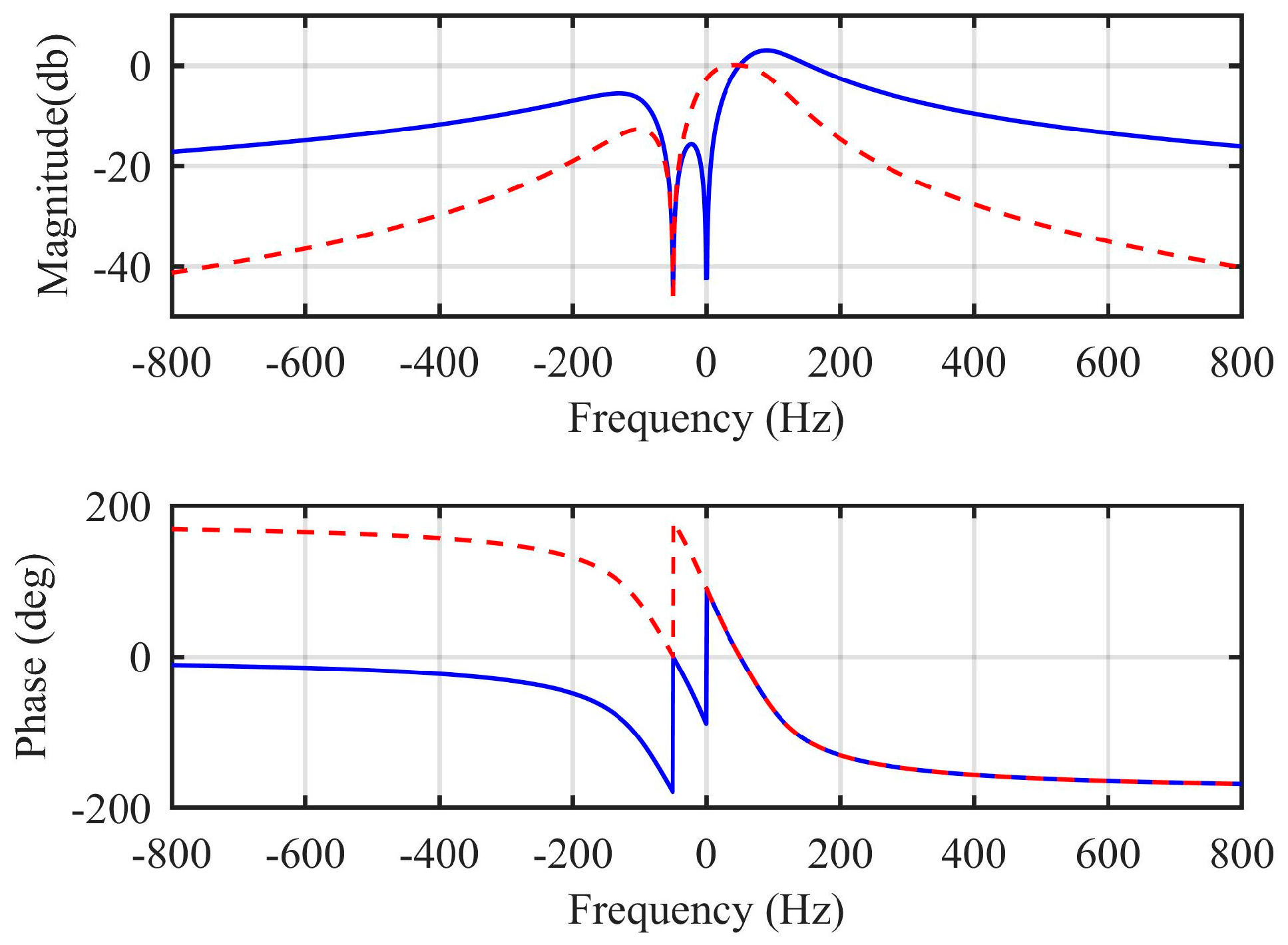
Figure 4 shows the bode plots for αβDMTOGI and DTOGI. The grid estimated frequency is 50 Hz. In the Figure 4, the red curve belongs to DTOGI(s), the blue curve is αβDMTOGI(s), and the values of k1 and k2 are 2.33 and 3.18, respectively [8]. According to Table 1 and Figure 4, it is found that the voltage disturbance component of −50 Hz in αβ-frame is eliminated using DTOGI, indicating that it can only reject the FFNS component of the grid voltage. While the voltage disturbance components at −50 Hz and 0 Hz in αβ-frame are completely eliminated by using αβDMTOGI. The gain of the FFPS component at 50 Hz is 0, and the phase is 0. This means that both the FFNS component and the DC offset of the grid voltage can be completely rejected by αβDMTOGI, and the amplitude and phase of the FFPS component are not affected at all.
αβDMTOGI eliminates the interference of FFNS component and DC offset component completely by using complex vector filter. However, αβDMTOGI can only restrain the high-frequency harmonics to some degree, but the harmonics components cannot be completely filtered, which can be seen in Figure 4.
4. Design of Enhanced DSC
The transfer function of the conventional DSC in s domain is
where n is the delay factor and T is the grid voltage fundamental period. n is the only adjustable parameter in conventional DSC [11].
In this paper, a new Modified DSC (MDSC) operator is employed [27], its transfer function is
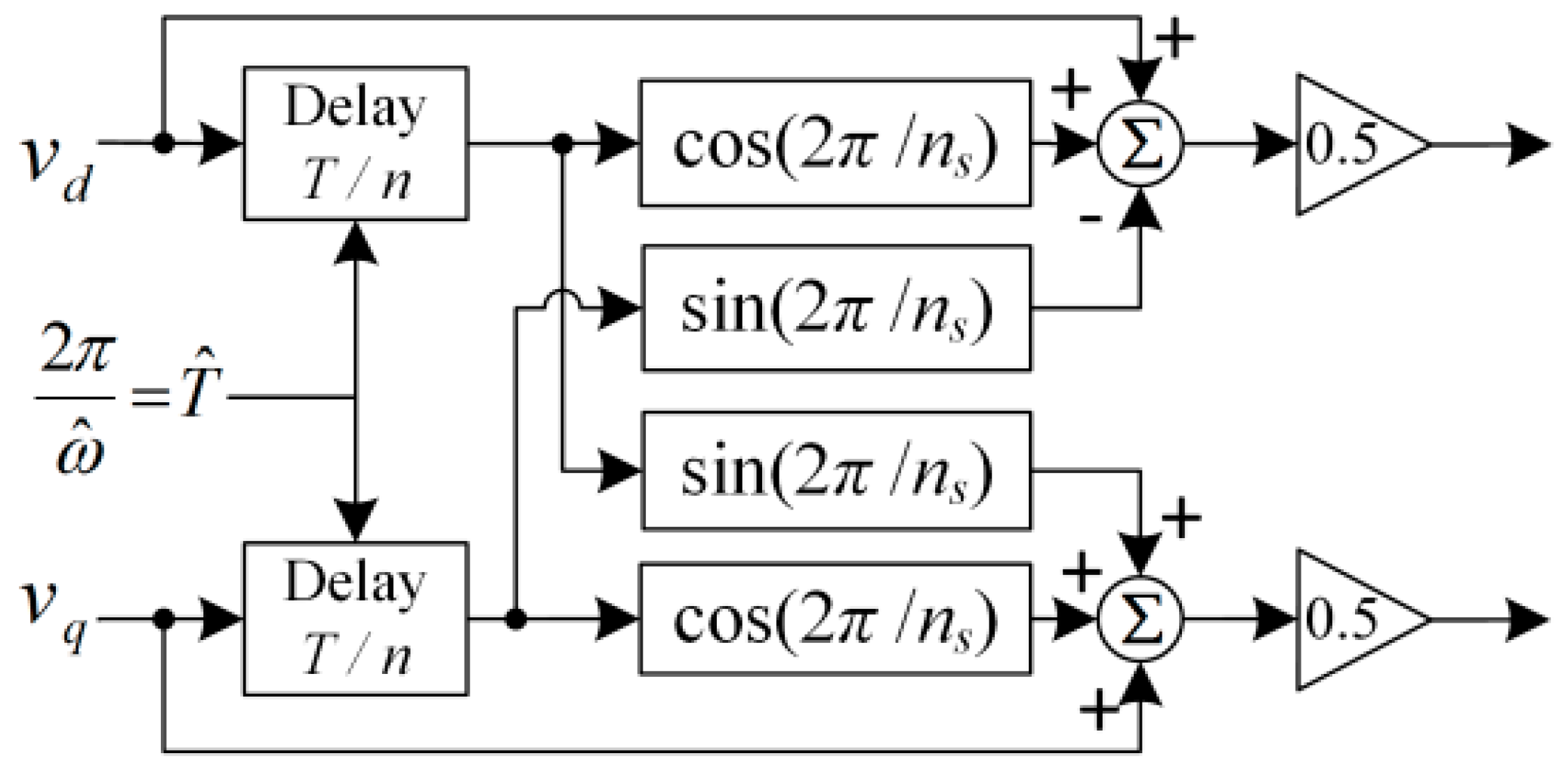
Unlike conventional DSC, MDSC has n, ns two parameters that can be adjusted to meet the requirements of the frequency characteristics. The role of ns is to shift the frequency characteristics of the conventional DSC on the frequency axis. The time domain implementation of MDCS is shown in Figure 5.
In this paper, the two parameters of MDSC, n and ns are set to be 6 and 2, respectively. The transfer function of the corresponding MDSC is
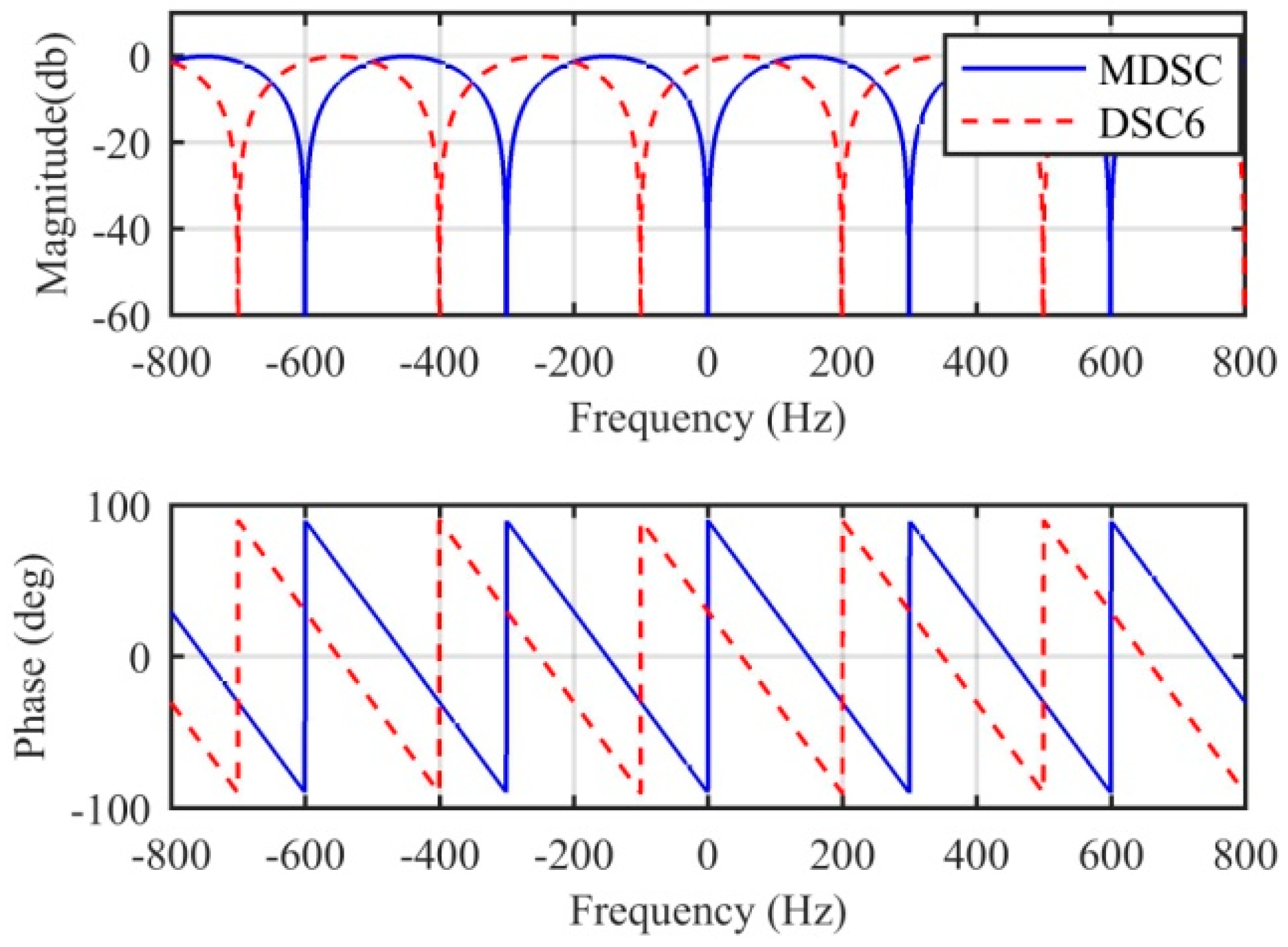
Figure 7 is the bode plot of the MDSC and DSC6. It can be observed that the frequency characteristic of the MDSC can be seen as the frequency characteristic of the DSC6 moving left 200 Hz on the frequency axis. As also can be seen in Figure 7, MDSC can completely block the harmonic components at ±300 Hz, ±600 Hz and other frequencies in the dq frame, but at the same time, the FFPS component at 0 Hz is also blocked.
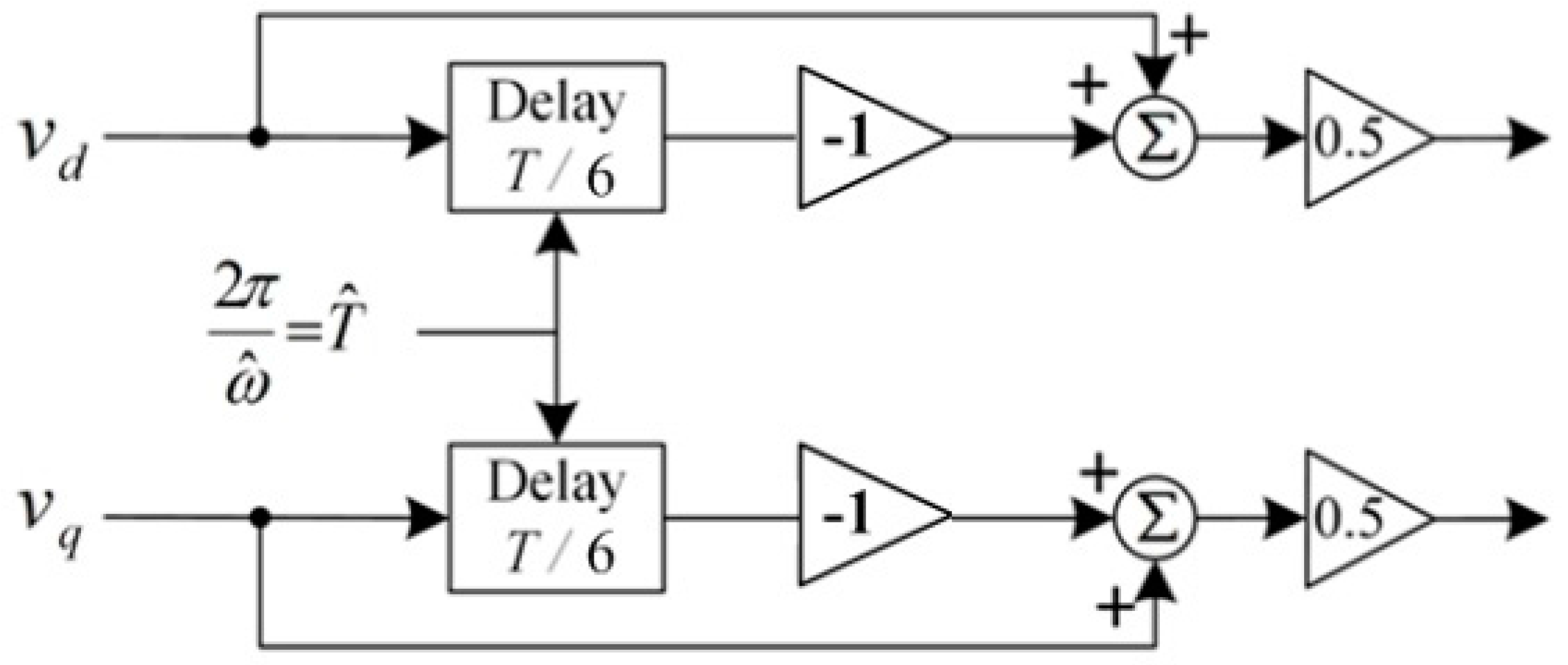
In order to retain the FFPS completely, this paper proposes an enhanced DSC (EDSC) by using the first-order low-pass filters (LPF) in parallel with the MDSC. The implementation form is shown in the Figure 8.
LPF expression is kc/s + kc, kc for the cutoff frequency, . Because LPF and MDSC are in parallel, the transfer function of EDSC is
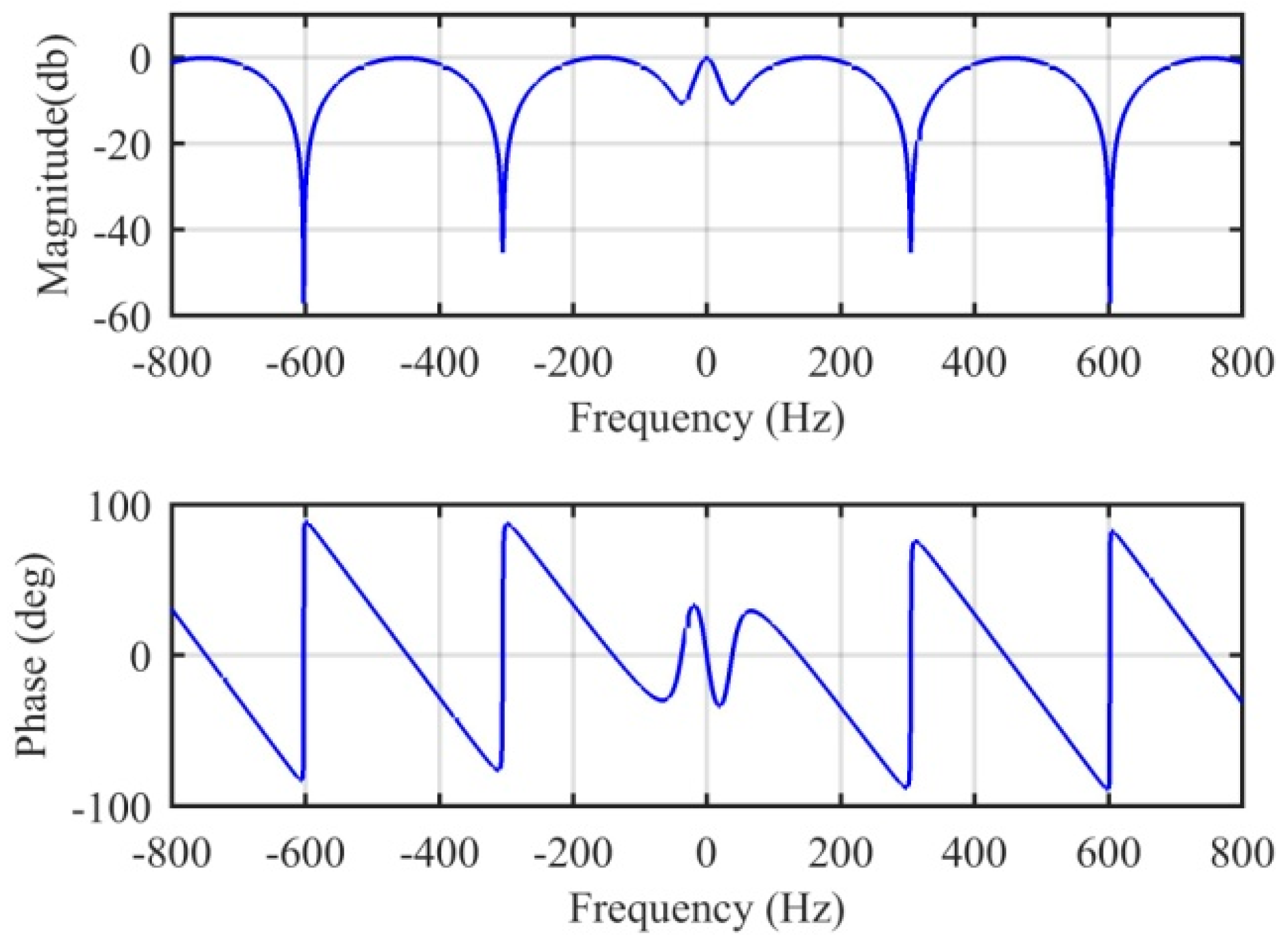
where is the estimated frequency of the grid and is 50 Hz. is the bandwidth adjustment coefficient, considering the low-pass filter response speed and bandwidth width, the value of is set to be 0.7. The bode plot of the EDSC is shown in Figure 9.
Conventional DSC-based PLLs usually adopt cascading multiple DSCs structure, but the EDSC has only one DSC operator, which can improve system response speed and significantly reduce the computational burden of the PLL. It can be seen from Figure 9, the FFPS magnification at 0 Hz is 1, and the phase is 0. In dq frame, it means that the magnitude and phase of the grid voltage FFPS are not affected.
5. Hybrid Filter in the Proposed PLL
5.1. Design of Hybrid Filter Based on DMTOGI and EDSC
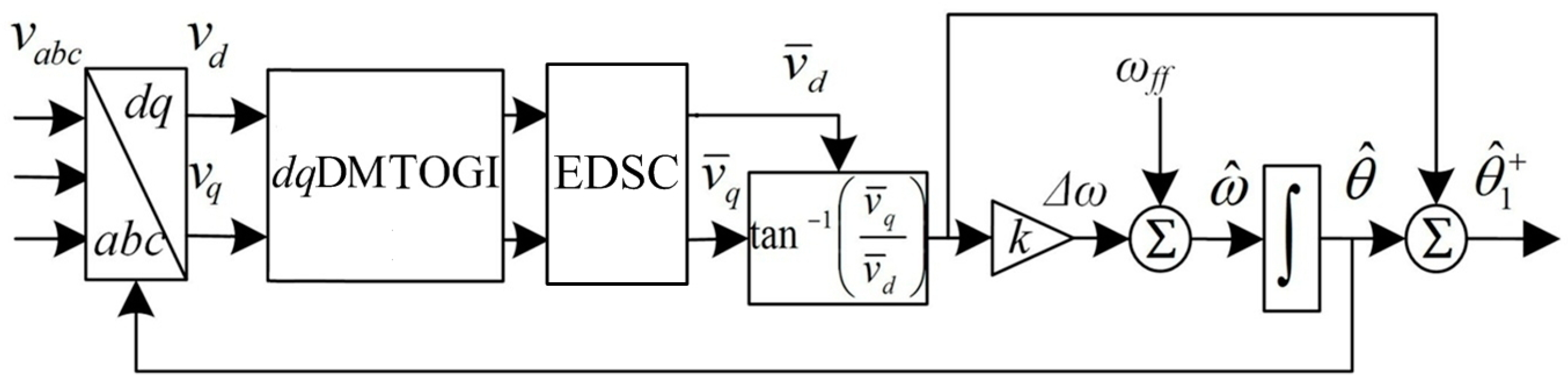
In order to eliminate the effects of high frequency harmonics to the SRF-PLL completely, αβDMTOGI is transformed into the dq-frame to achieve the dqDMTOGI, which is cascaded with the EDSC to form a hybrid filter. Then incorporate the hybrid filter into the SRF-PLL control inner loop to form a new three-phase PLL. Figure 10 shows the structure of the proposed PLL.
According to Table 1, dqDMTOGI is used to reject FFNS component at −100 Hz and the DC offset component at −50 Hz in dq-frame, and other harmonic components are rejected by EDSC.
The proposed approach of this paper transforms DMTOGI to the dq-frame and its transfer function in the dq-frame can be obtained by substituting s in αβDMTOGI (s) for [24].
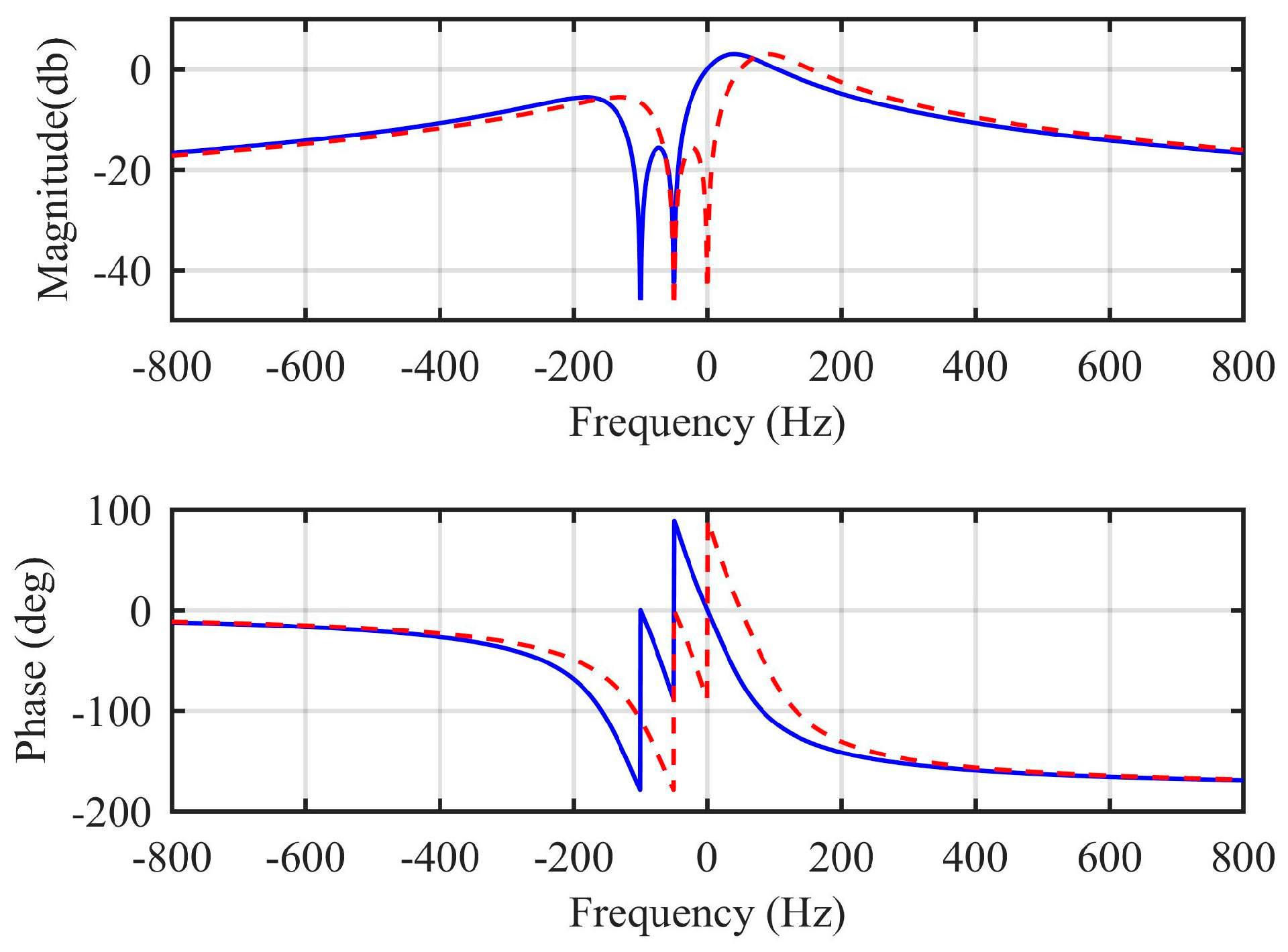
The frequency characteristics of αβDMTOGI(s) and the proposed dqDMTOGI(s) are shown in Figure 11. The red curve belongs to αβDMTOGI(s), whose notch frequencies are 0 Hz and −50 Hz. The blue curve belongs to dqDMTOGI(s), whose notch frequencies are −100 Hz z and −50 Hz. It can be observed that the characteristic curve of dqDMTOGI(s) is shifted left 50 Hz by corresponding to the characteristic curve of αβDMTOGI(s).
According to Figure 1 and Equation (4), the real part R(s) and the imaginary part Q(s) of complex transformation function can be achieved after mathematical manipulation to the dqDMTOGI(s) as
where , , k1 = 2.33, k2 = 3.18.
As the part cascaded with dqDMTOGI, the transfer function of EDSC has been given by Equation (16). Furthermore, the transfer function of the hybrid filter consisted with dqDMTOGI and EDSC can be written as
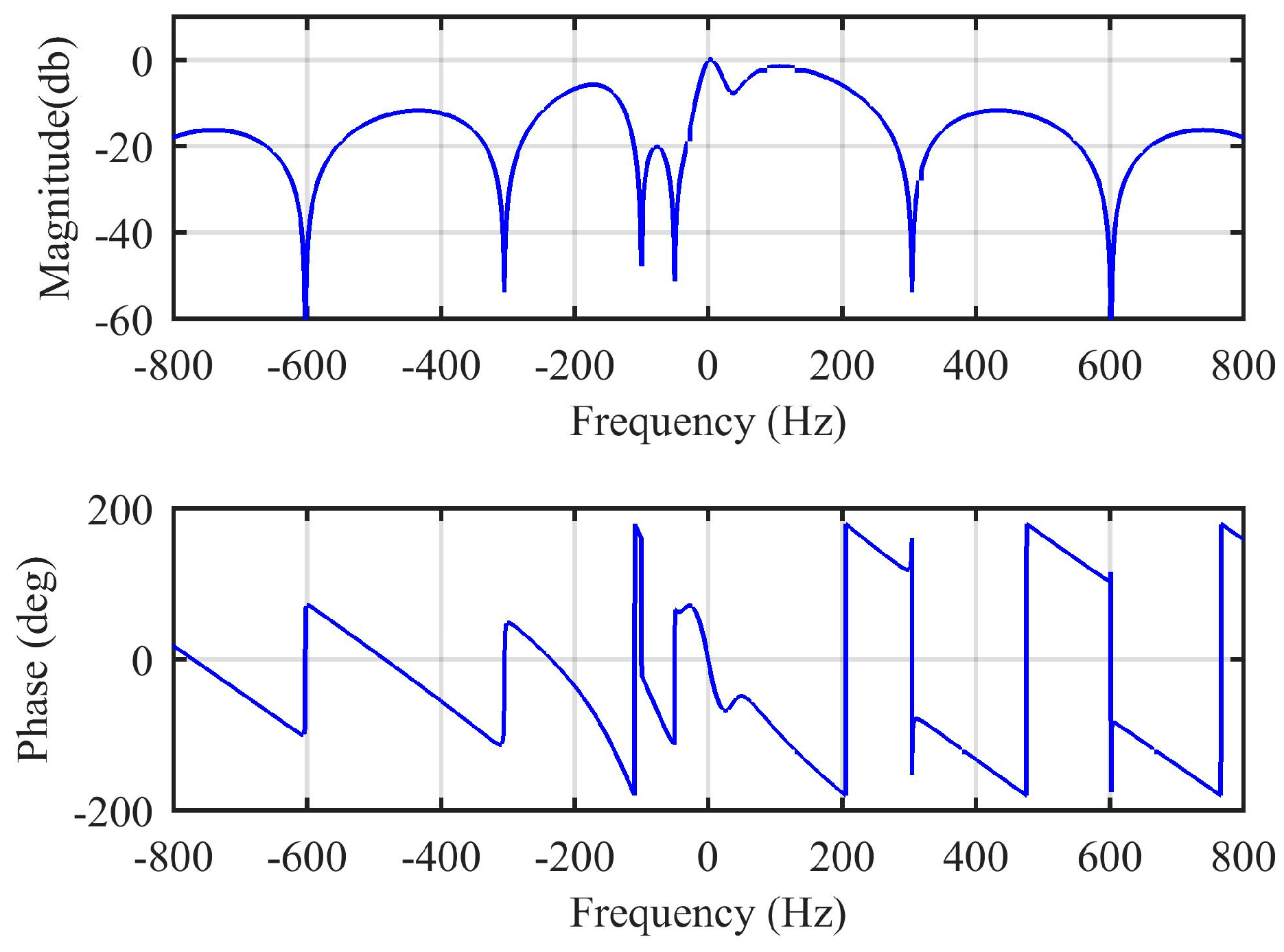
According to (20), Figure 12 shows the frequency response curve of the proposed hybrid filter. It can be found that the hybrid filter H(s) can block the FFNS component, DC offset component and other harmonic disturbance components of the grid voltage completely in Table 1. The FFPS component of the grid voltage in the dq-frame (the component at 0 Hz in the dq frame) without any frequency shifted, and the amplification factor is 1.
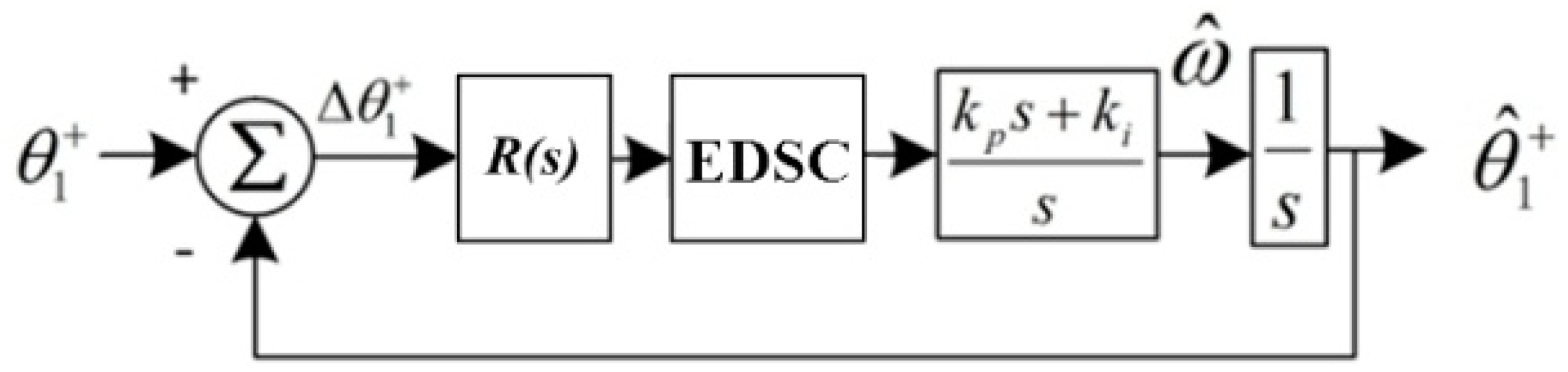
5.2. Small-Signal Model
The SRF-PLL based on DMTOGI and EDSC in this paper has been proposed in Figure 10. Figure 13 shows the small-signal model of the proposed PLL. According to the modeling method in reference [26], the real part R(s) of dqDMTOGI(s) is employed instead of dqDMTOGI for mathematical modeling. Its modeling accuracy will be verified later by simulation
5.3. Parameter Design Guidelines
The system open-loop transfer function in Figure 13 is
In Equation (21), EDSC(s) contains the delay link. This paper adopts the first-order Pade approximation approach to make the following equivalent of the Gol(s) delay link as
So
It is complicated to analyze and design PLL due to the high-order components in Equation (21). According to the reduction equivalent approach of higher-order PLL system in reference [28], this paper adopts the Pade approximation reduction approach in reference [29] to equivalent R(s) EDSC(s) as the first order transfer function.
The system open loop transfer function is
Applying the symmetric optimal design method in reference [16] to design the PI controller parameters for Equation (25), the two parameters of the PI controller are
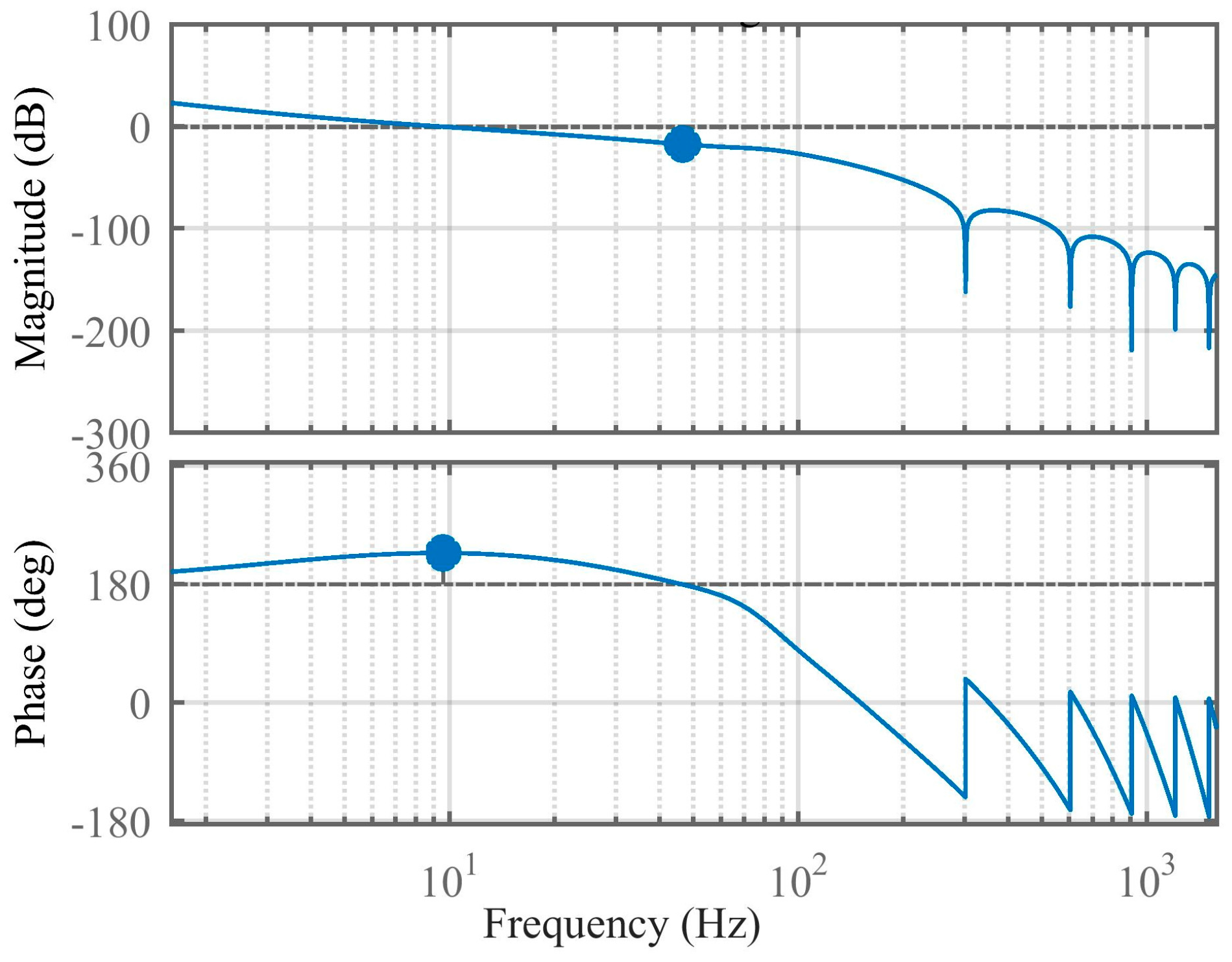
where C = 138.44, b is the parameter that affects the phase margin of the system. Usually, b is set to be 1 +, the corresponding controller parameters kp and ki are 57.3 and 1363.1, respectively. Figure 14 shows the system open-loop transfer function bode plot. The phase margin is 46.8° and the corresponding frequency is 9.58 Hz. The amplitude margin is 16.9 dB, the corresponding frequency is 46.5 Hz, so the system stability can be ensured.
5.4. Accuracy of Small-Signal Model
To verify the accuracy of the small-signal model, this section verifies the small-signal model and the actual proposed PLL waveform by establishing a simulation comparison under MATLAB/Simulink. In the simulation, the phase error under phase jump of 10° and frequency jump of +1 Hz are compared respectively, as shown in Figure 15. It can be seen that the small-signal can describe the proposed PLL in this paper precisely.
6. Experimental Results
To verify the tracking performance of the PLL under adverse grid conditions, phase jump, frequency step change, DC offset injection, unbalanced and distorted grid voltages experiments are carried out in this paper. The experiments are based on the DSP TMS320F28335. Arbitrary waveform generator manufactured by this DSP is used to generate three-phase voltage signals. The sampling frequency of the whole experiment is 10 kHz. The three-phase voltage nominal frequency is set to be 50 Hz, and the amplitude is normalized to 1 p.u. In the programming, the Adams–Bashforth method in [30] is used to ensure the accuracy of the discrete system model and avoid algebraic loop. The corresponding relation between the integral link of the continuous domain and the discrete domain is
Since the proposed PLL method is based on the DTOGI-PLL structure and EDSC approach, for the sake of comparison, DTOGI-PLL [8] and EGDSC-PLL [15] which is a new DSC approach with optimal dynamic performance in recent years are also implemented. The k1 and k2 in reference [8] were selected to obtain similar dynamic characteristics to DSOGI-PLL, but [8] did not specifically design them, so we select the parameters of DSOGI-PLL in reference [24] to design DTOGI-PLL specifically. The parameter design processes of the EGDSC-PLL is presented in [15]. The control parameters of the PLLs included in the experiments are summarized in Table 2.
6.1. Phase Jump
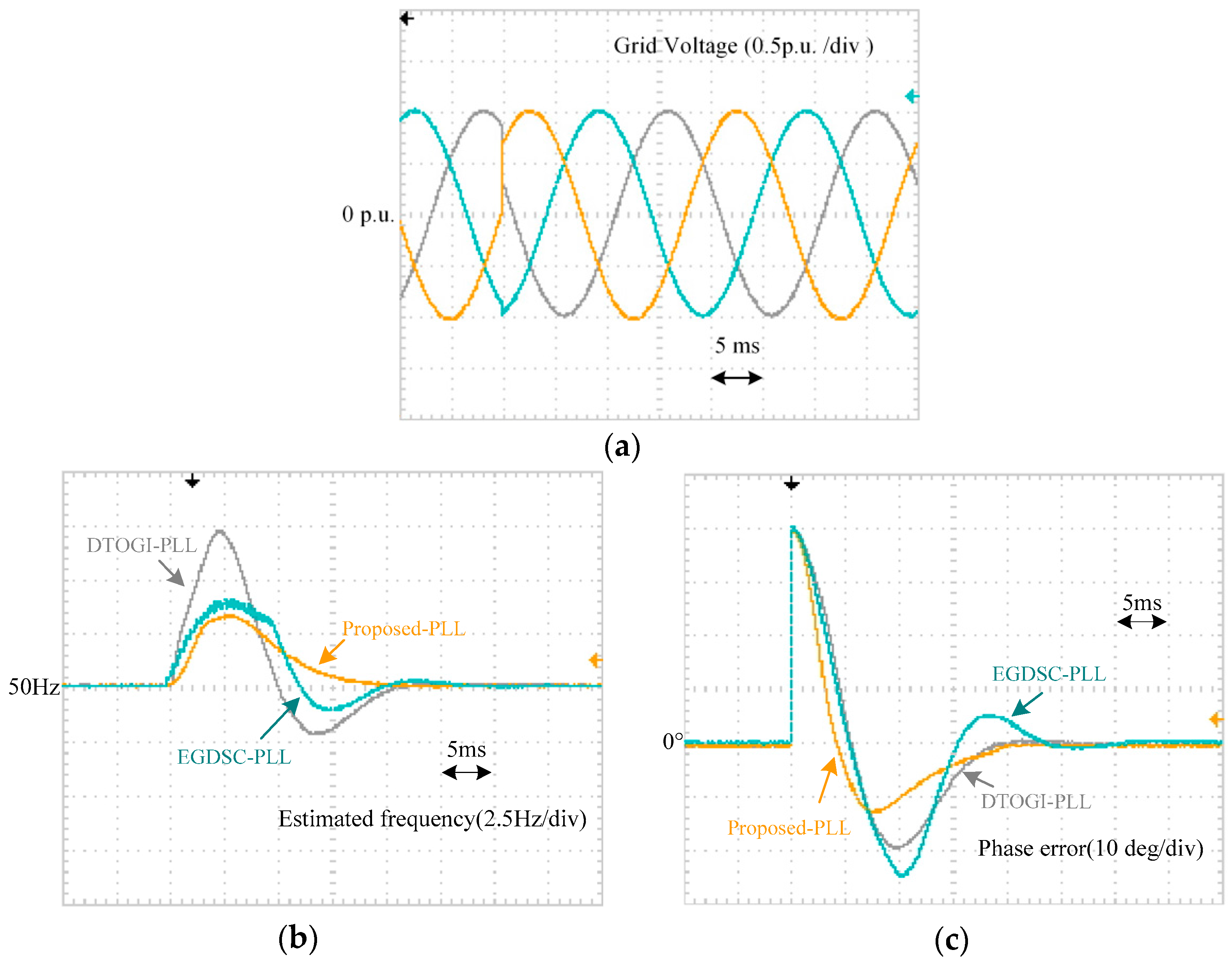
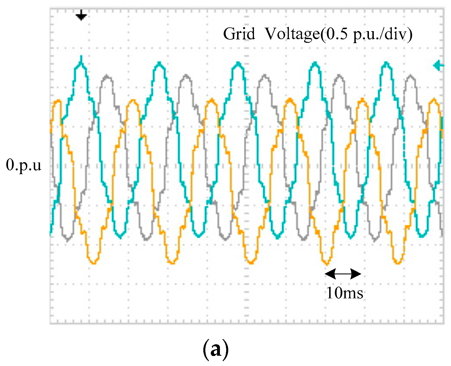
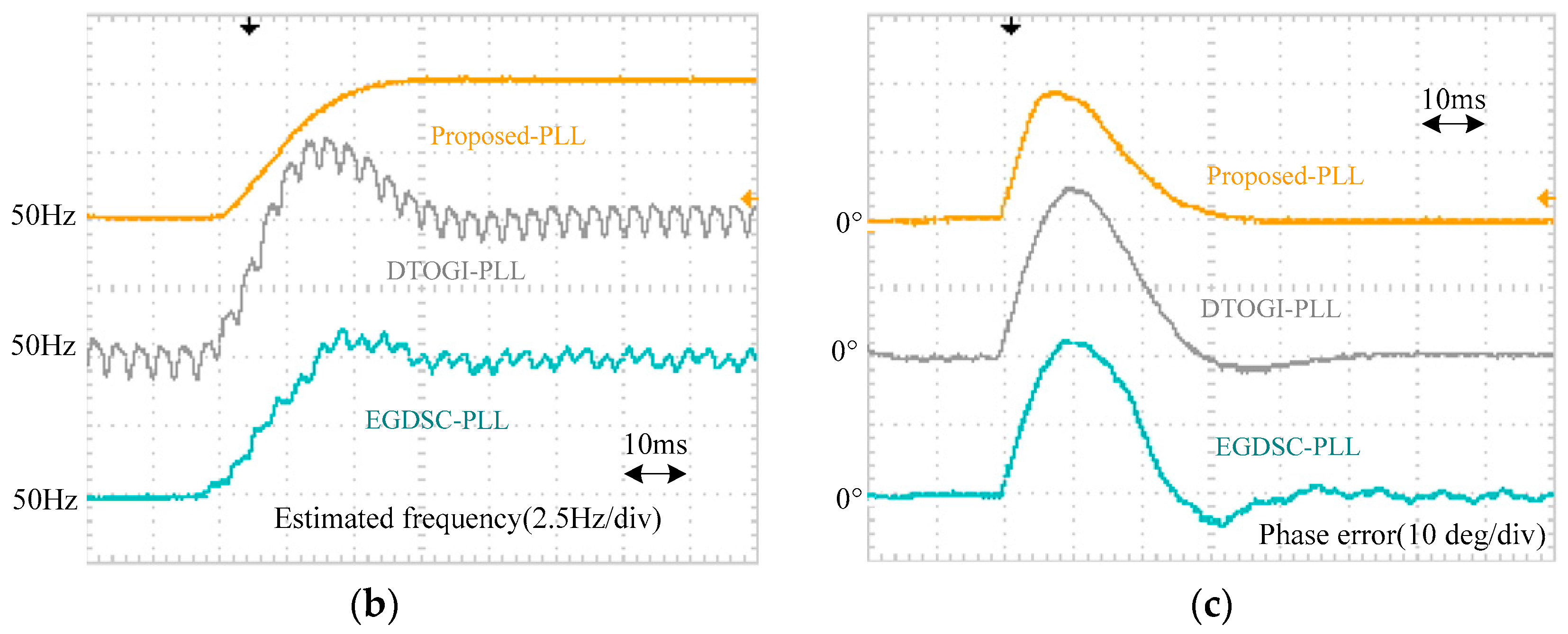
Figure 16 shows the experimental waveforms when the grid voltage undergoes a phase jump of +40°. It can be seen from Figure 16 that the proposed PLL in this paper has the shortest settling time, which is around 0.9 cycles. The other two PLLs settling time is about 20 ms. The settling time of the three PLLs meets the requirements of grid regulation for transient response of grid-connected devices. However, DTOGI-PLL has grid frequency estimation overshoot which will violate the grid frequency fluctuation restrict [31].
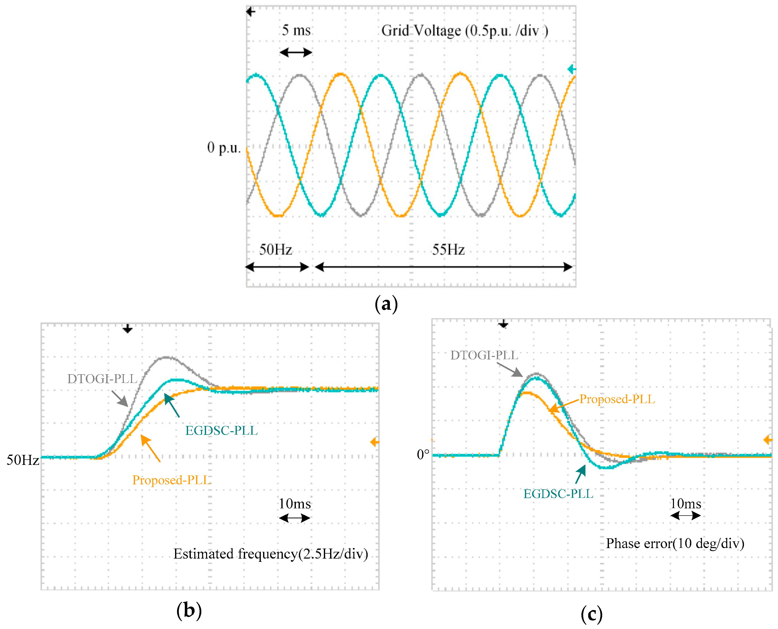
6.2. Frequency Step Change
Figure 17 shows the experimental waveforms when the grid voltage undergoes a frequency step change of +5 Hz. It can be observed from Figure 17b, the proposed PLL achieves the accurate estimate of the grid frequency after approximately 1.5 cycles, whereas DTOGI-PLL and EGDSC-PLL take a longer time. There is frequency overshoot of +2.5 Hz and +0.5 Hz for DTOGI-PLL and EGDSC-PLL, respectively. However, the proposed PLL has no overshoot problem in frequency estimation. As can be seen in Figure 17c, the proposed PLL recovers the phase tracking of the grid after approximately 1.5 cycles, the response speed is faster than the other two PLLs.
6.3. DC Offset Inject
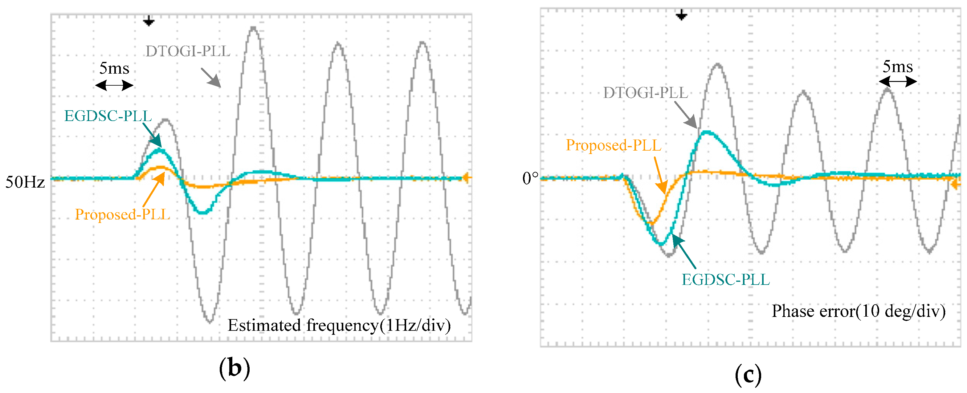
To evaluate the performance of the three PLLs when the grid voltage is mixed with DC components, the dc offset injection experiment is implemented. The injected value of phase A is 0.2 p.u., the injected value of phase B is 0.1 p.u., and the injected value of phase C is −0.2 p.u. Figure 18 shows the voltage waveform when the grid voltage is mixed with DC offset.
As shown in Figure 18, when the DC offset is injected into the three-phase voltages, both the phase estimation error and the frequency estimation of the three PLLs appear fluctuation. Taking the frequency shift less than 0.2 Hz as the standard, the proposed PLL recovers the accurate phase and frequency tracking in the shortest time, and the EGDSC-PLL is slightly slower. Since DTOGI-PLL does not have the ability to reject DC offset, its frequency estimation and phase error have a 50 Hz fundamental frequency oscillation.
6.4. Unbalanced and Distorted Grid Voltages
To evaluate the performance of the three PLLs when the grid voltage is distorted, the grid voltage distortion experiment is implemented. The injected harmonic voltage parameters are summarized in Table 3. In order to test the performance of the PLL when the grid frequency is changed, the frequency of the grid undergoes a +5 Hz frequency step change. Figure 19 shows the voltage waveform when the grid voltages are distorted.
It can be seen from Figure 19 that the proposed PLL can eliminate the effects of harmonic components completely. However, DTOGI-PLL filter stage is consisted of a low-pass filter, which can only suppress and not completely eliminate the harmonic interference. Therefore, both the frequency estimation and the phase estimation have an oscillation error caused by harmonics. In addition, EGDSC-PLL also has 2 Hz frequency estimation and 1° phase estimation oscillation errors because the filtering stage of EGDSC-PLL is composed of multiple DSCs, and they do not adopt frequency adaptive implementation.
6.5. Summary of Experimental Results
The dynamic performance of the proposed PLL is superior to the other two methods, and the reason is that the settling time of the proposed PLL is the shortest in the dynamic response process of all experiments. The proposed PLL can completely block the DC offset and harmonic caused by the non-ideal voltage and eliminate the oscillation error in phase and frequency estimation. Compared to the other two PLLs, the frequency estimation overshoot of the proposed PLL is the smallest when the grid voltage undergoes frequency step change.
The transient response of DTOGI-PLL is not as good as the other two PLLs, but it meets the requirement for grid connected equipment transient response. However, the biggest defect of DTOGI PLL is that it cannot block the harmonic under the non-ideal grid voltage condition completely. This is the reason that the filtering stage of DTOGI-PLL can be considered as a low pass filter. Another disadvantage is that DTOGI-PLL does not have DC offset rejection capability which cannot remove the influence of DC offset caused by grid voltage or signal acquisition stage.
The settling time of EGDSC-PLL is longer than the proposed PLL, but shorter than DTOGI-PLL. Owing to the EGDSC-PLL being composed of multiple DSCs which do not adopt frequency adaptive implementation, so the EGDSC-PLL has some frequency estimation and phase estimation oscillation errors.
7. Conclusions
In this paper, a MTOGI structure that can completely reject the DC offset component is proposed. In addition, an EDSC that can block the dominant harmonic components while reducing the number of DSC operators is also proposed. A new hybrid filter based-PLL is designed using the DMTOGI filter and the EDSC, the proposed PLL can block the FFNS component, the DC offset, and the dominant harmonics simultaneously. Compared with the conventional method, the proposed PLL has strong disturbance rejection ability, good filtering effect, and faster transient response. Simulation and experimental results verify the correctness and feasibility of the proposed PLL.
Acknowledgments
This work was supported in part by the national Natural Science Foundation of China (NSFC) under grant 61433004.
Author Contributions
Nanmu Hui and Dazhi Wang proposed the original idea; Nanmu Hui and Yunlu Li established the test bench and carried out the experiments. Nanmu Hui wrote the full manuscript and supervised the experiments.
Conflicts of Interest
The authors declare no conflict of interest.
References
- Ahmadzadeh, M.; Mortazavi, S.; Saniei, M. Applying the Taguchi Method for Investigating the Phase-Locked Loop Dynamics Affected by Hybrid Storage System Parameters. Energies 2018, 11, 226. [Google Scholar] [CrossRef]
- Cao, Y.; Yu, J.; Xu, Y.; Li, Y.; Yu, J. An Efficient Phase-Locked Loop for Distorted Three-Phase Systems. Energies 2017, 10, 280. [Google Scholar] [CrossRef]
- Luo, W.; Jiang, J.; Liu, H. Frequency-Adaptive Modified Comb-Filter-Based Phase-Locked Loop for a Doubly-Fed Adjustable-Speed Pumped-Storage Hydropower Plant under Distorted Grid Conditions. Energies 2017, 10, 737. [Google Scholar] [CrossRef]
- Xia, Y.; Douglas, S.; Mandic, D. Adaptive frequency estimation in smart grid applications: Exploiting noncircularity and widely linear adaptive estimators. IEEE Signal Proc. Mag. 2012, 29, 44–45. [Google Scholar] [CrossRef]
- Han, Y.; Xu, L.; Khan, M.; Yao, G.; Zhou, L.; Chen, C. A novel synchronization scheme for grid-connected converters by using adaptive linear optimal filter based PLL(ALOF-PLL). Simul. Model. Pract. Theory 2009, 17, 1299–1345. [Google Scholar] [CrossRef]
- Golestan, S.; Guerrero, J.; Vasquez, J. Three-Phase PLLs: A Review of Recent Advances. IEEE Trans. Power Electron. 2017, 32, 1894–1907. [Google Scholar] [CrossRef]
- Rodriguez, P.; Teodorescu, R.; Candela, I.; Timbus, A.; Liserre, M.; Blaabjerg, F. New positive-sequence voltage detector for grid synchronization of power converters under faulty grid conditions. In Proceedings of the 2006 37th IEEE Power Electronics Specialists Conference, Jeju, Korea, 18–22 June 2006; pp. 1–7. [Google Scholar]
- Li, W.; Ruan, X.; Bao, C.; Pan, D.; Wang, X. Grid synchronization systems of three-phase grid-connected power converters: A complex-vector-filter perspective. IEEE Trans. Ind. Electron. 2014, 61, 1855–1870. [Google Scholar] [CrossRef]
- Golestan, S.; Monfared, M.; Freijedo, F.; Guerrero, J. Performance Improvement of a Prefiltered Synchronous-Reference-Frame PLL by Using a PID-Type Loop Filter. IEEE Trans. Ind. Electron. 2014, 61, 3469–3479. [Google Scholar] [CrossRef]
- Wang, Y.; Li, Y. Grid synchronization PLL based on cascaded delay signal cancellation. IEEE Trans. Power Electron. 2011, 26, 1987–1997. [Google Scholar] [CrossRef]
- Golestan, S.; Ramezani, M.; Guerrero, J.; Monfared, M. dq-frame cascaded delayed signal cancellation-based PLL: Analysis, design, and comparison with moving average filter-based PLL. IEEE Trans. Power Electron. 2015, 30, 1618–1632. [Google Scholar] [CrossRef]
- Huang, Q.; Rajashekara, K. An improved delayed signal cancellation PLL for fast grid synchronization under distorted and unbalanced grid condition. IEEE Trans. Ind. Electron. 2017, 53, 4985–4997. [Google Scholar] [CrossRef]
- Wang, Y.; Li, Y. Three-phase cascaded delay signal cancellation PLL for fast selective harmonic detection. IEEE Trans. Ind. Electron. 2013, 60, 1452–1463. [Google Scholar] [CrossRef]
- Neves, F.; De Souza, H.; Cavalcanti, M.; Bradaschia, F.; Bueno, E. Digital filters for fast harmonic sequence component separation of unbalanced and distorted three-phase signals. IEEE Trans. Ind. Electron. 2012, 59, 3847–3859. [Google Scholar] [CrossRef]
- Golestan, S.; Freijedo, F.; Vidal, A.; Yepes, A.; Guerrero, J.; Doval-Gandoy, J. An efficient implementation of generalized delayed signal cancellation PLL. IEEE Trans. Power Electron. 2016, 31, 1085–1094. [Google Scholar] [CrossRef]
- Golestan, S.; Guerrero, J.; Gharehpetian, G. Five approaches to deal with problem of dc offset in phase-locked loop algorithm: Design considerations and performance evaluations. IEEE Trans. Power Electron. 2016, 31, 648–661. [Google Scholar] [CrossRef]
- Golestan, S.; Guerrero, J.; Vasquez, J. DC-Offset Rejection in Phase-Locked Loops: A Novel Approach. IEEE Trans. Ind. Electron. 2016, 63, 4942–4946. [Google Scholar] [CrossRef]
- Xie, M.; Wen, H.; Zhu, C.; Yang, Y. DC Offset Rejection Improvement in Single-Phase SOGI-PLL Algorithms: Methods Review and Experimental Evaluation. IEEE Access 2017, 5, 12810–12819. [Google Scholar] [CrossRef]
- Li, Y.; Wang, D.; Ning, Y.; Hui, N. DC-offset elimination method for grid synchronisation. Electron. Lett. 2017, 53, 335–337. [Google Scholar] [CrossRef]
- Luo, S.; Wu, F. Improved Two-Phase Stationary Frame EPLL to Eliminate Effect of Input Harmonics, Unbalance and DC offsets. IEEE Trans. Ind. Inform. 2017, 13, 2855–2863. [Google Scholar] [CrossRef]
- Xin, Z.; Wang, X.; Qin, Z.; Lu, M.; Loh, P.; Blaabjerg, F. An improved second-order generalized integrator based quadrature signal generator. IEEE Trans. Power Electron. 2016, 31, 8068–8073. [Google Scholar] [CrossRef]
- Wang, J.; Jun, L.; Feng, G.; Zhang, L.; Wang, Z. A Method to Improve the Dynamic Performance of Moving Average Filter-Based PLL. IEEE Trans. Power Electron. 2015, 30, 5978–5990. [Google Scholar] [CrossRef]
- Ma, C.; Gao, F.; He, G.; Li, G. Fast DC component suppression method for phase locked loop. In Proceedings of the 2014 IEEE Applied Power Electronics Conference and Exposition–APEC 2014, Fort Worth, TX, USA, 16–20 March 2014; pp. 2700–2705. [Google Scholar]
- Golestan, S.; Monfared, M.; Freijedo, F. Design-oriented study of advanced synchronous reference frame phase-locked loops. IEEE Trans. Power Electron. 2013, 28, 765–778. [Google Scholar] [CrossRef]
- Gonzalez-Espin, F.; Figueres, E.; Garcera, G. An adaptive synchronous-reference-frame phase-locked loop for power quality improvement in a polluted utility grid. IEEE Trans. Ind. Electron. 2012, 59, 2718–2731. [Google Scholar] [CrossRef]
- Li, Y.; Wang, D.; Han, W.; Tan, S.; Guo, X. Performance improvement of quasi-type-1 PLL by using a complex notch filter. IEEE Access 2016, 4, 6272–6282. [Google Scholar] [CrossRef]
- Li, Y.; Wang, D.; Han, W.; Sun, Z.; Yuan, T. A hybrid filtering stage based quasi-type-1 PLL under distorted grid conditions. J. Power Electron. 2017, 17, 704–715. [Google Scholar] [CrossRef]
- Golestan, S.; Freijedo, F.; Guerrero, J. A Systematic Approach to Design High-Order Phase-Locked Loops. IEEE Trans. Power Electron. 2015, 30, 2885–2890. [Google Scholar] [CrossRef]
- Golub, G.; Van Loan, C. Matrix Computations; Johns Hopkins University Press: Baltimore, MD, USA, 1989; pp. 557–558. [Google Scholar]
- Ciobotaru, M.; Teodorescu, R.; Blaabjerg, F. A new single-phase PLL structure based on second order generalized integrator. In Proceedings of the 2006 37th IEEE Power Electronics Specialists Conference, Jeju, Korea, 18–22 June 2006; pp. 1–6. [Google Scholar]
- Hadjidemetriou, L.; Kyriakides, E.; Blaabjerg, F. An adaptive tuning mechanism for phase-locked loop algorithm for faster time performance of interconnected renewable energy sources. IEEE Trans. Ind. Appl. 2015, 51, 1792–1804. [Google Scholar] [CrossRef]
Figure 1.
Complex vector filter. (a) Description of complex vector filter; (b) Implementation diagram of the complex vector filter.
Figure 1.
Complex vector filter. (a) Description of complex vector filter; (b) Implementation diagram of the complex vector filter.

Figure 2.
The implementation of TOGI and MTOGI. (a) TOGI; (b) MTOGI.

Figure 3.
Block diagram of DMTOGI.

Figure 4.
Bode diagram of αβDMTOGI and DTOGI.

Figure 5.
Time-domain implementation of the MDSC.

Figure 6.
Simplified time-domain implementation of the MDSC.

Figure 7.
Bode diagram of MDSC (solid lines) and DSC6 (dashed lines).

Figure 8.
Time-domain implementation of the EDSC.

Figure 9.
Bode diagram of EDSC.

Figure 10.
Block diagram of the proposed PLL in this paper.

Figure 11.
Bode diagram of αβDMTOGI(s) and dqDMTOGI(s).

Figure 12.
Bode diagram of the hybrid filter.

Figure 13.
Small-signal model of the proposed PLL.

Figure 14.
Open-loop bode plot of the proposed PLL.

Figure 15.
Performance comparison between proposed-PLL and its small-signal model under (a) a phase jump of +10°, and (b) a frequency jump of +1 Hz.
Figure 15.
Performance comparison between proposed-PLL and its small-signal model under (a) a phase jump of +10°, and (b) a frequency jump of +1 Hz.

Figure 16.
Experimental waveforms when the grid voltage undergoes a phase jump of +40. (a) is the grid voltage waveform, (b) is the estimated frequency waveform, and (c) is the phase error waveform.
Figure 16.
Experimental waveforms when the grid voltage undergoes a phase jump of +40. (a) is the grid voltage waveform, (b) is the estimated frequency waveform, and (c) is the phase error waveform.

Figure 17.
Experimental waveforms when the grid voltage undergoes a frequency step change of +5 Hz. (a) is the grid voltage waveform, (b) is the estimated frequency waveform, and (c) is the phase error waveform.
Figure 17.
Experimental waveforms when the grid voltage undergoes a frequency step change of +5 Hz. (a) is the grid voltage waveform, (b) is the estimated frequency waveform, and (c) is the phase error waveform.

Figure 18.
Experimental waveforms when the grid voltage is mixed with DC offset. (a) is the grid voltage waveform, (b) is the estimated frequency waveform, and (c) is the phase error waveform.
Figure 18.
Experimental waveforms when the grid voltage is mixed with DC offset. (a) is the grid voltage waveform, (b) is the estimated frequency waveform, and (c) is the phase error waveform.


Figure 19.
Experimental waveforms when the grid voltages are distorted with a frequency step change of +5 Hz. (a) is the grid voltage waveform, (b) is the estimated frequency waveform, and (c) is the phase error waveform.
Figure 19.
Experimental waveforms when the grid voltages are distorted with a frequency step change of +5 Hz. (a) is the grid voltage waveform, (b) is the estimated frequency waveform, and (c) is the phase error waveform.


Table 1.
Dominant components of the grid voltage.
| Harmonic order | … | −11 | −6 | −1 | 0 | +1 | +7 | +13 | … |
| αβ-frame (Hz) | … | −550 | −250 | −50 | 0 | 50 | 350 | 650 | … |
| Harmonic order | … | −12 | −6 | −2 | −1 | 0 | +6 | +12 | … |
| dq-frame (Hz) | … | −600 | −300 | −100 | −50 | 0 | 300 | 600 | … |
Table 2.
PLLs’ control parameters.
| Parameters | Proposed-PLL | DTOGI-PLL | EGDSC-PLL |
|---|---|---|---|
| Damping coefficient, ξ | - | 1 | 1 |
| Bandwidth adjustment coefficient, σ | 0.7 | - | - |
| Proportional coefficient, kp | 57.3 | 141.2 | 440 |
| Integral coefficient, ki | 1363.1 | 9928 | 48,361 |
Table 3.
Parameters of grid voltages.
| Voltage Component (in αβ-Frame) | Amplitude (p.u.) |
|---|---|
| Fundamental positive sequence | 1 |
| Fundamental negative sequence | 0.1 |
| 5th harmonic negative sequence | 0.1 |
| 7th harmonic positive sequence | 0.05 |
| 11th harmonic negative sequence | 0.05 |
| 13th harmonic positive sequence | 0.05 |
© 2018 by the authors. Licensee MDPI, Basel, Switzerland. This article is an open access article distributed under the terms and conditions of the Creative Commons Attribution (CC BY) license (http://creativecommons.org/licenses/by/4.0/).
Share and Cite
MDPI and ACS Style
Hui, N.; Wang, D.; Li, Y. An Efficient Hybrid Filter-Based Phase-Locked Loop under Adverse Grid Conditions. Energies 2018, 11, 703. https://0-doi-org.brum.beds.ac.uk/10.3390/en11040703
AMA Style
Hui N, Wang D, Li Y. An Efficient Hybrid Filter-Based Phase-Locked Loop under Adverse Grid Conditions. Energies. 2018; 11(4):703. https://0-doi-org.brum.beds.ac.uk/10.3390/en11040703
Chicago/Turabian StyleHui, Nanmu, Dazhi Wang, and Yunlu Li. 2018. "An Efficient Hybrid Filter-Based Phase-Locked Loop under Adverse Grid Conditions" Energies 11, no. 4: 703. https://0-doi-org.brum.beds.ac.uk/10.3390/en11040703
Note that from the first issue of 2016, this journal uses article numbers instead of page numbers. See further details here.