
Lithography Processable Ta2O5 Barrier-Layered Chitosan Electric Double Layer Synaptic Transistors


Department of Electronic Materials Engineering, Kwangwoon University, 447-1, Wolgye-dong, Nowon-gu, Seoul 139-701, Korea
*
Author to whom correspondence should be addressed.
Int. J. Mol. Sci. 2021, 22(3), 1344; https://0-doi-org.brum.beds.ac.uk/10.3390/ijms22031344
Submission received: 29 December 2020
/
Revised: 25 January 2021
/
Accepted: 27 January 2021
/
Published: 29 January 2021
(This article belongs to the Special Issue Chitosan Functionalizations, Formulations and Composites 2.0)
Abstract
:We proposed a synaptic transistor gated using a Ta2O5 barrier-layered organic chitosan electric double layer (EDL) applicable to a micro-neural architecture system. In most of the previous studies, a single layer of chitosan electrolyte was unable to perform lithography processes due to poor mechanical/chemical resistance. To overcome this limitation, we laminated a high-k Ta2O5 thin film on chitosan electrolyte to ensure high mechanical/chemical stability to perform a lithographic process for micropattern formation. Artificial synaptic behaviors were realized by protonic mobile ion polarization in chitosan electrolytes. In addition, neuroplasticity modulation in the amorphous In–Ga–Zn-oxide (a-IGZO) channel was implemented by presynaptic stimulation. We also demonstrated synaptic weight changes through proton polarization, excitatory postsynaptic current modulations, and paired-pulse facilitation. According to the presynaptic stimulations, the magnitude of mobile proton polarization and the amount of weight change were quantified. Subsequently, the stable conductance modulation through repetitive potential and depression pulse was confirmed. Finally, we consider that proposed synaptic transistor is suitable for advanced micro-neural architecture because it overcomes the instability caused when using a single organic chitosan layer.
1. Introduction
Neural systems are efficient information-processing systems. Moreover, the mammalian brain contains approximately 100 billion neurons with 100 trillion synapses. With this particular network structure, our brain performs massively parallel and distributed computations by combining memory and processing capacities with an ultra-low power consumption of 20 W [1,2]. Inspired by this mechanism, the neuromorphic chip technology implemented in semiconductors is receiving increasing attention. In particular, synaptic transistors mimicking the synaptic behavior of the human brain are core elements of a neuromorphic chip [3]. The characteristics of these synaptic transistors can be emulated using an electric double layer (EDL) as the gate dielectric layer. High-density charges in the EDL accumulate even at very low voltages, which can respond to synaptic spikes through strong capacitance coupling effects [4,5]. A candidate for this EDL is the proton-conductive chitosan electrolyte with obvious advantages. Chitosan is obtained from chitin, the second most abundant organic biopolymer on the earth. As a biodegradable and renewable bio-friendly material, chitosan has great potential for skin-attachable and implantable neuromorphic chips [6]. Moreover, owing to the EDL effect of proton-conductive chitosan electrolyte, high gate capacitance (>1.0 µF/cm2) can be easily obtained from high-density mobile protons, enabling synaptic behavior [7,8]. Nevertheless, chitosan electrolytes suffer from processing capability inconveniences such as low chemical/mechanical resistance and ambient instabilities, which are limitations of organics materials. These limitations are rigorous obstacles in the implementation of practical electronic devices using chitosan. The application of organic chitosan EDL to transistors, which are basic components of electronic circuits, represents a major challenge in (complementary metal–oxide–semiconductor) CMOS process compatibilities.
Therefore, in this study, we propose amorphous In–Ga–Zn-oxide (a-IGZO) channel synaptic transistors gated by a high-k Ta2O5 barrier-layered organic chitosan EDL for a micro-neural architecture. The synaptic behaviors are emulated using the organic chitosan electrolyte EDL for polarization reaction by mobile protonic ions. Moreover, the inorganic high-k Ta2O5 barrier layer improves the chemical resistance and mechanical strength, enabling CMOS process compatibility and stably transferring presynaptic spikes to the postsynaptic a-IGZO channel. Ta2O5 is widely known as a biocompatible material and enhances its advantages in implementing human-friendly neuromorphic chips with chitosan [9,10]. Consequently, this study shows the possibility of implementing micro-neural structures and synaptic functions by overcoming the limitations of organic EDLs, which are expected to be useful for developing advanced neural networks.
2. Results and Discussion
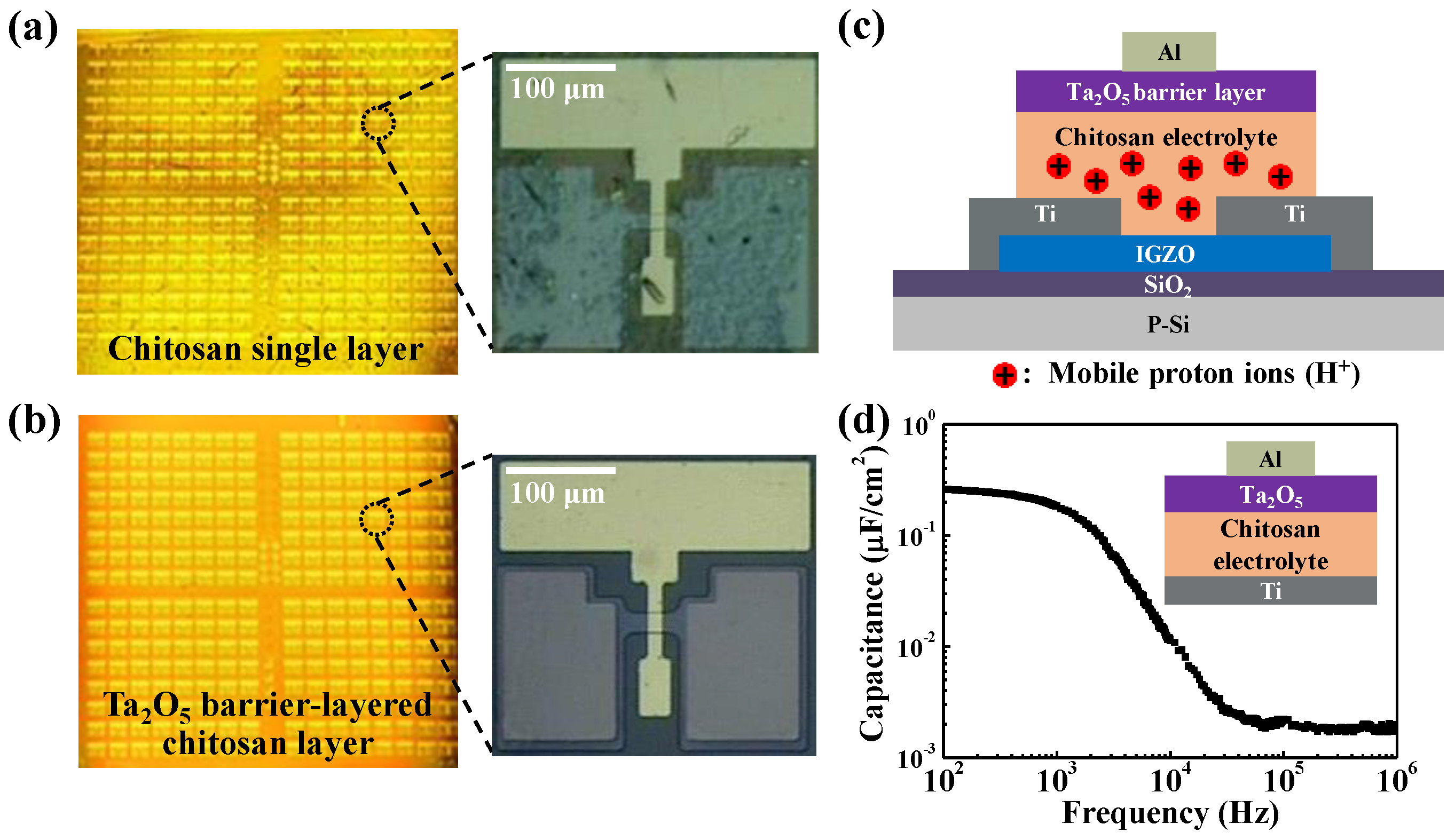
Figure 1a shows the optical microscopic images of the top-gate structure chitosan electrolyte synaptic transistor without the Ta2O5 barrier layer. In the pattern image, the swelling and outgassing appearing in the chitosan EDL and source/drain (S/D) contact hole etching are incomplete due to the damaged chitosan EDL. In contrast, Figure 1b shows that the Ta2O5 barrier layer laminated chitosan electrolyte synaptic transistor can withstand the process of (ultraviolet) UV exposure and baking during the photolithography due to the Ta2O5 barrier. This implies that the Ta2O5 high-k thin film is an essential barrier ensuring the advanced patterning process by preventing damage to the organic chitosan electrolyte layer. Figure 1c shows the cross-sectional schematic diagrams of the top-gate structure Ta2O5 barrier-layered chitosan EDL synaptic transistor. Most of the previously reported chitosan-electrolyte synaptic transistors were fabricated by a simple patterning process using a shadow mask [11,12,13,14,15]. Figure 1d shows the specific capacitance of Ta2O5 barrier-layered chitosan electrolyte film as a function of frequency. It is observed that there is a strong electric-double layer (EDL) effect by mobile ion at the chitosan electrolyte interface with a high EDL capacitance of ~0.26 µF cm−2 at 100 Hz. Table 1 reports on the latest studies of synaptic transistors that applied chitosan electrolyte as an EDL. As the device is fabricated through a precise photolithography patterning process, it has a relatively small channel size compared to previous studies that applied a shadow mask.
Figure 2a shows the double-sweep transfer characteristic (ID–VG) curves at a constant drain voltage (VD) of 1 V. The maximum gate bias (VG_max) increases positively (forward) from 0 to 10 V in increments of 0.5 V and sweeps back negatively (reverse). The counter-clockwise hysteresis in the double-bias ID–VG curve increases with increasing VG_max due to the slow polarization reaction by the mobile protons of the chitosan electrolyte [19]. The larger the VG_max, the larger the electric field, the stronger the dipole alignment, and the stronger the ion accumulation, resulting in a uniform increase in the hysteresis window. The inset in the figure shows the output characteristic (ID–VD) curves measured at VG–Vth from 0 to 10 V in increments of 1 V. As the VD increases, the drain current increases linearly and then gradually saturates, indicating ohmic contact and pinch-off characteristics. Figure 2b shows the threshold voltage and hysteresis window of the double-sweep ID–VG curve, according to VG_max. The threshold voltage remains almost constant as VG_max varies, while the hysteresis window shows a slope of 0.82 V/V and linearity (R2) of 99.05 when VG_max increases. Moreover, when VG_max decreases, a slope of −0.79 V/V and an R2 of 99.23 can be obtained. These results suggest that the polarization response of the mobile protons is uniform in the Ta2O5 laminated chitosan EDL.
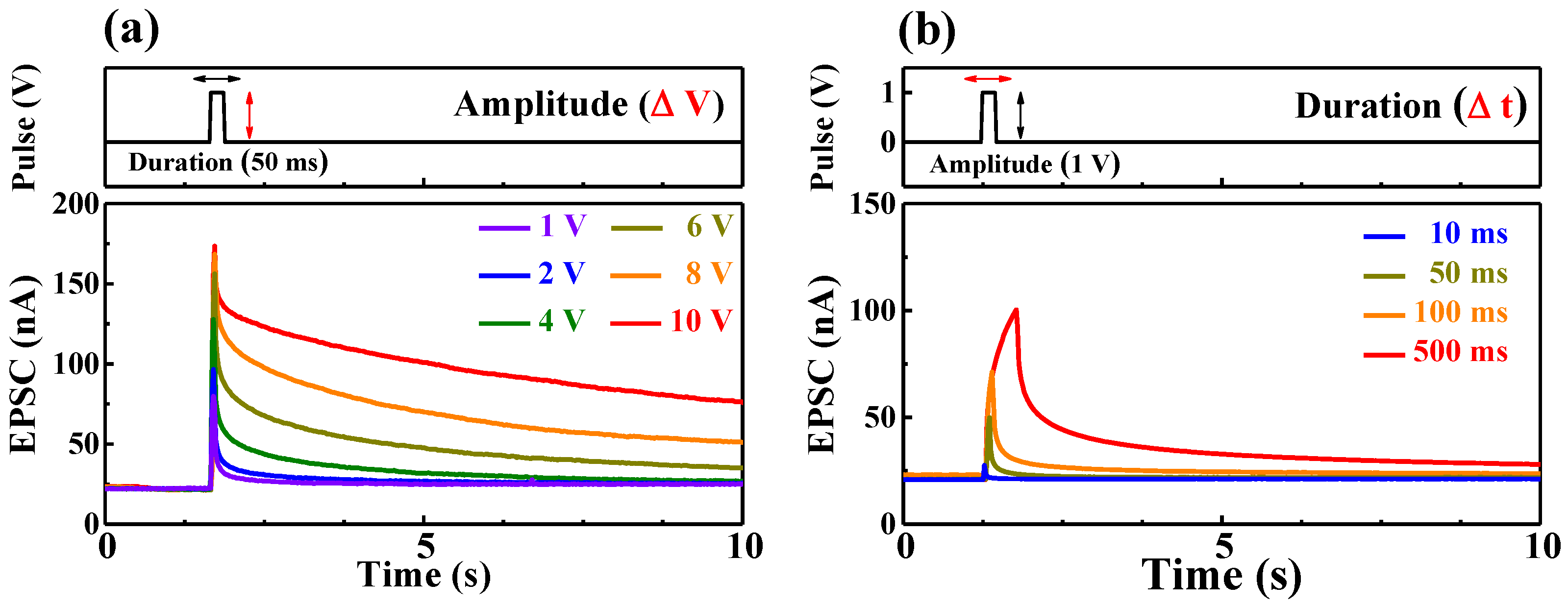
In synaptic transistors, the gate voltage and channel conductance are considered as presynaptic stimulus and synaptic weight, respectively. The excitatory postsynaptic current (EPSC) caused by a single synaptic spike represents a fundamental neuromorphic property of the synaptic transistors. Moreover, a single synaptic spike repetition affects the postsynaptic short-term plasticity (STP) and the long-term plasticity (LTP) and significantly affects long-term weight formation [20]. Figure 3a,b shows the EPSC retention characteristics for a single gate pulse with amplitude (under fixed duration) and duration (under fixed amplitude) as variables, respectively. After a single gate stimulation, the EPSC of the postsynaptic channel gradually decreases from a peak value corresponding to the intensity of each stimulation. Furthermore, the magnitude of the residual EPSC increases as the amplitude and duration of the gate pulse increase. When the presynaptic spike amplitude and duration are low, the EPSC is maintained by the slow polarization reaction of the mobile protons inside the chitosan EDL. In contrast, when the spike amplitude is high, protons partially penetrate the a-IGZO channel layer. The increased channel conductance and long resting time due to electrochemical doping of the a-IGZO channel indicate the controllability of the synaptic weight from STP to LTP [21]. Therefore, the higher the pulse stimulation, the larger the weight capacity to mimic the behavior of the human brain. Therefore, the modulation of EPSC due to two or multiple consecutive spikes plays an essential function in decoding temporal information in biological systems [22].
Figure 4a shows the EPSC triggered by two consecutive presynaptic spikes (1 V-amplitude, 50 ms-duration) with an interval of 60 ms. The paired-pulse facilitation (PPF) index corresponds to the amplification ratio between A1 and A2, the magnitude of the first and second EPSC peaks. Figure 4b shows the PPF index according to the interval time of two consecutive presynaptic spikes. At an interval of 50 ms, the PPF index is ~161%. However, above 1500 ms, the index decreases to ~100%. If the interval time is short, some mobile protons, accumulated at the interface between the electrolyte and the channel, do not have enough time to diffuse back before the arrival of the second spike. Therefore, the EPSC response of the second spike is stronger than that of the first spike [18]. The PPF index curve can be fitted considering the following double-phase exponential function [23,24]:
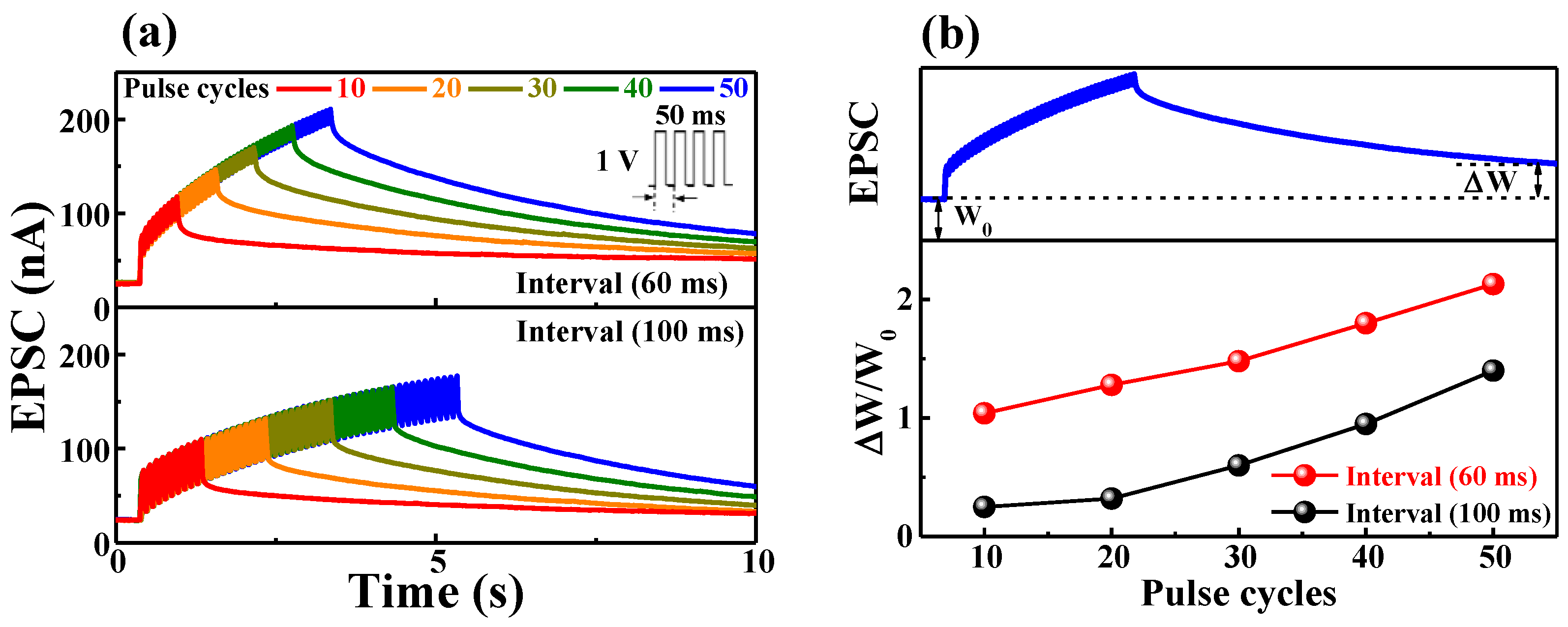
where Δt is the interval time between two consecutive presynaptic spikes. C1 and C2 are the initially facilitated magnitudes of the respective phases. τ1 and τ2 are the characteristic relaxation times, in this case, estimated as 13 ms and 402 ms, respectively. These results are similar to the time scale of biological synapses [25]. In a real synaptic operation, as the signals are transmitted and processed by multiple pulses [26], the identification of the postsynaptic response by multiple presynaptic pulses is essential. Figure 5a shows the EPSC response as a function of multiple presynaptic stimulation spikes at different pulse interval times. The EPSC value and resting time increase with the number of presynaptic spikes. In particular, multiple pulses with a short pulse interval of 60 ms have higher peak and residual EPSC values than those with a pulse longer than 100 ms. A practical method to identify a change in the synaptic response is by identifying the change in the synaptic weight. In artificial neural networks, the learning process is performed by adjusting synaptic weight values [27]. Figure 5b shows the change in the synaptic weight obtained by dividing the change occurring in the steady EPSC state after 10 s of the occurrence of stimulation (∆W) by that in the initial EPSC state before stimulation (W0) [28,29]. At the pulse interval of 100 ms, the change in the synaptic weight of 50 spikes is 1.4, while at the shorter interval of 60 ms, a significant change of 2.1 is observed. This result implies that a short pulse interval is insufficient for mobile protons to diffuse back before the next spike and successive pulses increase the synaptic weight. Thus, it is verified that the learning process of artificial neural networks could be controlled by adjusting the presynaptic spike interval.
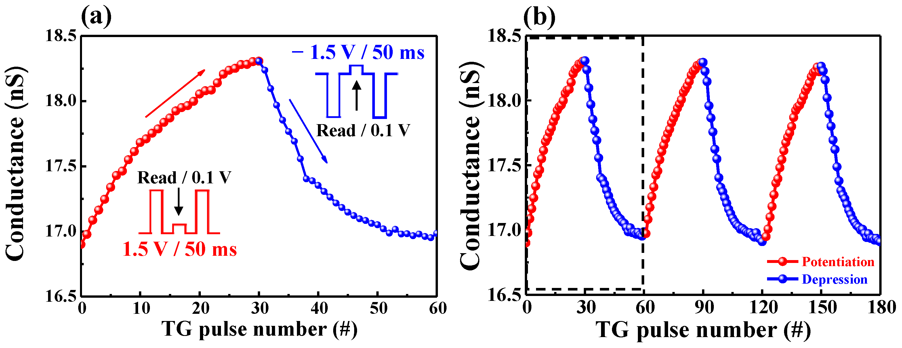
Until now, we focused on the time-dependent learning mechanism. When this mechanism prologues, updating the weights is critical for matrix multiplication in artificial neural networks. They remain constant until the next update [30]. Figure 6a shows the continuous conductance modulation as a variation of the presynaptic pulse number. The steady conductance increment and decrement (indicating biological synaptic potentiation and depression) were evaluated by applying a repetitive positive presynaptic pulse (1.5 V for 50 ms), and negative presynaptic pulse (−1.5 V for 50 ms) at 0.1 V read voltage, respectively. Through 30 pulses, the conductance in the channel was modulated in the dynamic range of ~1.5 nS. Figure 6b shows the conductance retention when this potentiation and depression cycles are repeated three times. When comparing the first cycle and the third cycle, the conductance peak value was 99.7%, indicating stable operation.
3. Materials and Methods
3.1. Materials
A (100)-oriented p-type silicon wafer (resistivity range between 1−10 Ω·cm, LG SILTRON Inc., Gumi, Korea). IGZO sputter target (In2O3:Ga2O3:ZnO = 4:2:4.1 mol%, THIFINE, Incheon, Korea). 30:1 buffered oxide etchant (J.T. Baker, Phillipsburg, USA). Ti fillet (purity >99.999%, THIFINE, Seoul, Korea). Chitosan powder (from shrimp shell, deacetylation degree >75%, Sigma Aldrich Inc, Seoul, Korea). Acetic acid solution (purity >99%, Sigma Aldrich). Ta2O5 sputter target (THIFINE). Al fillet (purity >99.999%, THIFINE)
3.2. Fabrication Methods of Ta2O5 Barrier-Layered Chitosan EDL Transistor
A (100)-oriented p-type silicon wafer with a 100-nm-thick thermally grown SiO2 layer was cleaned following the standard (radio corporation of America) RCA process. For the channel layer (postsynapse), a 50 nm thick a-IGZO layer was deposited using radio frequency (RF) magnetron sputtering with an IGZO target (In2O3:Ga2O3:ZnO = 4:2:4.1 mol%). The active channel region with width/length = 20/10 μm for the a-IGZO synaptic transistor was developed by photolithography and wet etching with 30:1 buffered oxide etchant (BOE). For source/drain (S/D) electrodes, a 150 nm thick Ti film was deposited by an e-beam evaporator and patterned using the lift-off method. The organic chitosan EDL, the core material of the proposed synaptic device, was formed by the following procedure. The organic layer was formed using a 2 wt% chitosan electrolyte solution dissolved in 2 wt% acetic acids; the layer was spin coated, dried in air ambient for 24 h, and oven-baked at 130 °C for 10 min. The thickness of the chitosan EDL was 130 nm (±5 nm in deviation). A high-k Ta2O5 dielectric layer 80 nm thick was deposited by RF magnetron sputtering as a chemical/mechanical barrier layer of the organic chitosan electrolyte film. The top-gate electrode, serving as a presynapse, was formed using an e-beam evaporator and lift-off of a 150 nm thick Al film over the chitosan–Ta2O5 laminated gate dielectric. Finally, the S/D contact holes were opened by a reactive ion etching (RIE) process. Note that every patterning process for the fabrication of the organic chitosan–EDL-based synaptic transistors was performed by lithography.
3.3. Characterization of Devices
The optical microscope image of the fabricated Ta2O5 barrier-layered chitosan EDL transistor was analyzed using an SV−55 Microscope System (SOMETECH, Seoul, Korea). The frequency-dependent specific capacitance of Ta2O5–chitosan electrolyte EDL capacitor was analyzed using an 4284A Precision LCR meter (Hewlett-Packard Co., Palo Alto, CA, USA). The Transfer and output characteristics and synaptic behavior of Ta2O5 barrier-layered chitosan EDL transistor were measured using an Agilent 4156B Precision Semiconductor Parameter Analyzer (Hewlett-Packard Co., USA). The device measurement was conducted on a probe station in a dark box to avoid any light and electrical noises. To apply a presynaptic spike, electrical pulses were applied by Agilent 8110A Pulse Generator (Hewlett-Packard Co., USA).
4. Conclusions
In summary, we fabricated a top-gate structure synaptic transistor in which an inorganic Ta2O5 high-k thin film was laminated on an organic chitosan electrolyte EDL using a lithography process. We also showed artificial synaptic behavior based on protonic mobile ion polarization in chitosan electrolytes. The laminated Ta2O5 barrier layer effectively transmits top-gate (presynaptic) spikes to the chitosan electrolyte and a-IGZO channels (postsynaptic), while improving chemical resistance and mechanical strength for CMOS process compatibility. The double-sweep transfer curves of the a-IGZO synaptic transistor showed counter-clockwise hysteresis due to the uniform and stable polarization reaction and the back diffusion of mobile proton ions in the chitosan electrolyte. Moreover, the excitatory behavior control characteristics of the a-IGZO channel for artificial neural networks were verified by adjusting the presynaptic pulse amplitude, duration, and interval. Therefore, the proposed synaptic transistor is expected to be useful for implementing advanced micro-neural structure systems by providing CMOS process compatibility.
Author Contributions
Conceptualization, S.-H.K. and W.-J.C.; investigation, S.-H.K. and W.-J.C.: writing—original draft preparation, S.-H.K. and W.-J.C.; writing—review and editing, S.-H.K. and W.-J.C.; supervision, W.-J.C.; project administration, W.-J.C.; funding acquisition, W.-J.C. All authors have read and agreed to the published version of the manuscript.
Funding
This work was supported by a National Research Foundation of Korea (NRF) grant funded in 2020 by the Korea government (MIST) (No. 2020R1A2C1007586). The work was also funded in 2020 and conducted under the Competency Development Program for Industry Specialists of the Korean Ministry of Trade, Industry and Energy (MOTIE), operated by Korea Institute for Advancement of Technology (KIAT) (No. P0002397, HRD program for Industrial Convergence of Wearable Smart Devices).
Institutional Review Board Statement
Not applicable.
Informed Consent Statement
Not applicable.
Data Availability Statement
The data presented in this study are available from the corresponding author upon reasonable request.
Conflicts of Interest
The authors declare no conflict of interest.
References
- Li, H.K.; Chen, T.P.; Liu, P.; Hu, S.G.; Liu, Y.; Zhang, Q.; Lee, P.S. A light-stimulated synaptic transistor with synaptic plasticity and memory functions based on InGaZnOx–Al2O3 thin film structure. J. Appl. Phys. 2006, 119, 244505. [Google Scholar] [CrossRef]
- Yang, R.; Terabe, K.; Yao, Y.; Tsuruoka, T.; Hasegawa, T.; Gimzewski, J.K.; Aono, M. Synaptic plasticity and memory functions achieved in a WO3−x- based nanoionics device by using the principle of atomic switch operation. Nanotechnology 2013, 24, 384003. [Google Scholar] [CrossRef] [PubMed]
- Guo, L.; Wen, J.; Cheng, G.; Yuan, N.; Ding, J. Synaptic behaviors mimicked in indium-zinc-oxide transistors gated by high-proton-conducting graphene oxide-based composite solid electrolytes. J. Mater. Chem. C 2014, 4, 9762–9770. [Google Scholar] [CrossRef]
- Yuan, H.; Shimotani, H.; Tsukazaki, A.; Ohtomo, A.; Kawasaki, M.; Iwasa, Y. High-density carrier accumulation in ZnO field-effect transistors gated by electric double layers of ionic liquids. Adv. Funct. Mater. 2009, 19, 1046–1053. [Google Scholar] [CrossRef]
- Zhou, B.; Sun, J.; Han, X.; Jiang, J.; Wan, Q. Low-voltage organic/inorganic hybrid transparent thin-film transistors gated by chitosan-based proton conductors. IEEE Electron Device Lett. 2011, 32, 1549–1551. [Google Scholar] [CrossRef]
- Liu, Y.H.; Zhu, L.Q.; Feng, P.; Shi, Y.; Wan, Q. Freestanding artificial synapses based on laterally proton-coupled transistors on chitosan membranes. Adv. Mater. 2015, 27, 5599–5604. [Google Scholar] [CrossRef]
- Dou, W.; Jiang, J.; Sun, J.; Zhou, B.; Wan, Q. Low-voltage oxide-based electric-double-layer TFTs gated by stacked electrolyte/chitosan hybrid dielectrics. IEEE Electron Device Lett. 2012, 33, 848–850. [Google Scholar] [CrossRef]
- Zhang, J.; Dai, J.; Zhu, L.; Chen, C.; Wan, Q. Laterally coupled IZO-based transistors on free-standing proton conducting chitosan membranes. IEEE Electron Device Lett. 2014, 35, 838–840. [Google Scholar] [CrossRef]
- Black, J. Biologic performance of tantalum. Clin. Mater. 1994, 16, 67–173. [Google Scholar] [CrossRef]
- Ding, Z.; Zhou, Q.; Wang, Y.; Ding, Z.; Tang, Y.; He, Q. Microstructure and properties of monolayer, bilayer and multilayer Ta2O5-based coatings on biomedical Ti-6Al-4V alloy by magnetron sputtering. Ceram. Int. 2020, 47, 1133–1144. [Google Scholar] [CrossRef]
- Zhou, J.; Liu, Y.; Shi, Y.; Wan, Q. Solution-processed chitosan-gated IZO-based transistors for mimicking synaptic plasticity. IEEE Electron Device Lett. 2014, 35, 280–282. [Google Scholar] [CrossRef]
- Yu, F.; Zhu, L.Q.; Gao, W.T.; Fu, Y.M.; Xiao, H.; Tao, J.; Zhou, J.M. Chitosan-based polysaccharide-gated flexible indium tin oxide synaptic transistor with learning abilities. ACS Appl. Mater. Interfaces 2018, 10, 16881–16886. [Google Scholar] [CrossRef] [PubMed]
- Wu, G.; Zhang, J.; Wan, X.; Yang, Y.; Jiang, S. Chitosan-based biopolysaccharide proton conductors for synaptic transistors on paper substrates. J. Mater. Chem. C 2014, 2, 6249–6255. [Google Scholar] [CrossRef]
- Feng, P.; Du, P.; Wan, C.; Shi, Y.; Wan, Q. Proton conducting graphene oxide/chitosan composite electrolytes as gate dielectrics for new-concept devices. Sci. Rep. 2016, 6, 34065. [Google Scholar] [CrossRef] [Green Version]
- Lu, G.; Liu, Y.; Lin, F.; Gen, K.; Wu, W.J.; Yao, R. Realization of artificial synapse and inverter based on oxide electric-double-layer transistor gated by a chitosan biopolymer electrolyte. Semicond. Sci. Technol. 2020, 35, 075014. [Google Scholar] [CrossRef]
- Ren, Z.Y.; Zhu, L.Q.; Yu, F.; Xiao, H.; Xiong, W.; Ge, Z.Y. Synaptic metaplasticity of protonic/electronic coupled oxide neuromorphic transistor. Org. Electron. 2019, 74, 304–308. [Google Scholar] [CrossRef]
- He, Y.; Nie, S.; Liu, R.; Shi, Y.; Wan, Q. Indium–gallium–zinc–oxide Schottky synaptic transistors for silent synapse conversion emulation. IEEE Electron Device Lett. 2018, 40, 139–142. [Google Scholar] [CrossRef]
- Yu, F.; Zhu, L.Q.; Xiao, H.; Gao, W.T.; Guo, Y.B. Restickable oxide neuromorphic transistors with spike-timing-dependent plasticity and pavlovian associative learning activities. Adv. Funct. Mater. 2018, 28, 1804025. [Google Scholar] [CrossRef]
- Zhu, L.Q.; Wan, C.J.; Guo, L.Q.; Shi, Y.; Wan, Q. Artificial synapse network on inorganic proton conductor for neuromorphic systems. Nat. Commun. 2014, 5, 1–7. [Google Scholar] [CrossRef] [Green Version]
- Ohno, T.; Hasegawa, T.; Tsuruoka, T.; Terabe, K.; Gimzewski, J.K.; Aono, M. Short-term plasticity and long-term potentiation mimicked in single inorganic synapses. Nat. Mater. 2011, 10, 591–595. [Google Scholar]
- Wen, J.; Zhu, L.Q.; Fu, Y.M.; Xiao, H.; Guo, L.Q.; Wan, Q. Activity dependent synaptic plasticity mimicked on indium–tin–oxide electric-double-layer transistor. ACS Appl. Mater. Interfaces 2017, 9, 37064–37069. [Google Scholar] [CrossRef] [PubMed]
- Buonomano, D.V.; Maass, W. State-dependent computations: Spatiotemporal processing in cortical networks. Nat. Rev. Neurosci. 2009, 10, 113–125. [Google Scholar] [CrossRef]
- Zucker, R.S.; Regehr, W.G. Short-Term Synaptic Plasticity. Annu. Rev. Physiol. 2002, 64, 355–405. [Google Scholar] [CrossRef] [PubMed] [Green Version]
- Zhao, S.; Ni, Z.; Tan, H.; Wang, Y.; Jin, H.; Nie, T.; Yang, D. Electroluminescent synaptic devices with logic functions. Nano Energy 2018, 54, 383–389. [Google Scholar] [CrossRef]
- Zhu, L.Q.; Wan, C.J.; Gao, P.Q.; Liu, Y.H.; Xiao, H.; Ye, J.C.; Wan, Q. Flexible proton-gated oxide synaptic transistors on Si membrane. ACS Appl. Mater. Interfaces 2016, 8, 21770–21775. [Google Scholar] [CrossRef] [PubMed]
- Byrne, J.H. Learning and Memory: A Comprehensive Reference; Academic Press: Cambridge, MA, USA, 2017. [Google Scholar]
- Kandel, E.R.; Schwartz, J.H.; Jessell, T.M. Principles of Neural Science; McGraw-Hill: New York, NY, USA, 2000; pp. 1227–1246. [Google Scholar]
- Yang, Y.; Wen, J.; Guo, L.; Wan, X.; Du, P.; Feng, P.; Wan, Q. Long-term synaptic plasticity emulated in modified graphene oxide electrolyte gated IZO-based thin-film transistors. ACS Appl. Mater. Interfaces 2016, 8, 30281–30286. [Google Scholar] [CrossRef] [PubMed]
- Shim, H.; Sim, K.; Ershad, F.; Yang, P.; Thukral, A.; Rao, Z.; Kim, H.J.; Liu, Y.; Wang, X.; Gu, G.; et al. Stretchable elastic synaptic transistors for neurologically integrated soft engineering systems. Sci. Adv. 2019, 5, eaax4961. [Google Scholar] [CrossRef] [Green Version]
- Zhong, G.; Zi, M.; Ren, C.; Xiao, Q.; Tang, M.; Wei, L.; An, F.; Xie, S.; Wang, J.; Zhong, X.; et al. Flexible electronic synapse enabled by ferroelectric field effect transistor for robust neuromorphic computing. Phys. Lett. A 2020, 117, 092903. [Google Scholar] [CrossRef]
Figure 1.
Optical microscope images of synaptic transistors fabricated by photolithography patterning process gated by (a) single chitosan layer and (b) high-k Ta2O5 barrier-layered chitosan layer; (c) cross-sectional schematics of Ta2O5–chitosan EDL transistor. (d) Frequency-dependent specific capacitance of the Ta2O5–chitosan electrolyte EDL capacitor.

Figure 2.
(a) Sequentially measured double-sweep ID−VG curves, according to maximum gate voltage increases (0 to 10 V in 0.5 V increments); the inset shows the ID−VD curves. (b) Threshold voltage and hysteresis window variation extracted from double sweep ID−VG curves, according to maximum gate voltage increased and then decreased.

Figure 3.
Excitatory postsynaptic current (EPSC) retention characteristics by a single gate pulse with (a) amplitude (1 to 10 V) variation for a fixed duration and (b) duration (10 to 500 ms) variation for a fixed amplitude.
Figure 3.
Excitatory postsynaptic current (EPSC) retention characteristics by a single gate pulse with (a) amplitude (1 to 10 V) variation for a fixed duration and (b) duration (10 to 500 ms) variation for a fixed amplitude.

Figure 4.
(a) EPSC triggered by a pair of pulses with a 60 ms interval; (b) paired-pulse facilitation (PPF) index (A2/A1) as a function of the pulse interval. The solid line corresponds to the fitting curve of the double-phase exponential function.
Figure 4.
(a) EPSC triggered by a pair of pulses with a 60 ms interval; (b) paired-pulse facilitation (PPF) index (A2/A1) as a function of the pulse interval. The solid line corresponds to the fitting curve of the double-phase exponential function.

Figure 5.
(a) EPSC recorded in response to presynaptic stimulation of multiple spikes (10–50 cycles); (b) change in synaptic weight according to the input pulse number. W0 is the initial EPSC before stimulation, and ∆W is the EPSC change after 10 s.
Figure 5.
(a) EPSC recorded in response to presynaptic stimulation of multiple spikes (10–50 cycles); (b) change in synaptic weight according to the input pulse number. W0 is the initial EPSC before stimulation, and ∆W is the EPSC change after 10 s.

Figure 6.
(a) Gradual conductance modulation by repeated synaptic potentiation (1.5 V for 50 ms) and depression (−1.5 V for 50 ms) pulses; (b) three cycles of repetitive conductance modulation.
Figure 6.
(a) Gradual conductance modulation by repeated synaptic potentiation (1.5 V for 50 ms) and depression (−1.5 V for 50 ms) pulses; (b) three cycles of repetitive conductance modulation.


Table 1.
Benchmark of synaptic transistors using chitosan electrolyte as an electric double layer.
| References | Gate Insulation Material | Structure Type | Channel Width/Length | Patterning Process |
|---|---|---|---|---|
| 2020 Ref. [15] | Chitosan | Bottom-gate type | 200 µm/200 µm | Shadow mask |
| 2019 Ref. [16] | Chitosan | Bottom-gate type | 1 mm/80 µm | Shadow mask |
| 2018 Ref. [17] | Chitosan | Bottom-gate type | 1 mm/80 µm | Shadow mask |
| 2018 Ref. [18] | Chitosan | Bottom-gate type | 1 mm/80 µm | Shadow mask |
| This study | Ta2O5 barrier Chitosan | Top-gate type | 20 µm/10 µm | Photolithography |
Publisher’s Note: MDPI stays neutral with regard to jurisdictional claims in published maps and institutional affiliations. |
© 2021 by the authors. Licensee MDPI, Basel, Switzerland. This article is an open access article distributed under the terms and conditions of the Creative Commons Attribution (CC BY) license (http://creativecommons.org/licenses/by/4.0/).
Share and Cite
MDPI and ACS Style
Kim, S.-H.; Cho, W.-J. Lithography Processable Ta2O5 Barrier-Layered Chitosan Electric Double Layer Synaptic Transistors. Int. J. Mol. Sci. 2021, 22, 1344. https://0-doi-org.brum.beds.ac.uk/10.3390/ijms22031344
AMA Style
Kim S-H, Cho W-J. Lithography Processable Ta2O5 Barrier-Layered Chitosan Electric Double Layer Synaptic Transistors. International Journal of Molecular Sciences. 2021; 22(3):1344. https://0-doi-org.brum.beds.ac.uk/10.3390/ijms22031344
Chicago/Turabian StyleKim, Sung-Hun, and Won-Ju Cho. 2021. "Lithography Processable Ta2O5 Barrier-Layered Chitosan Electric Double Layer Synaptic Transistors" International Journal of Molecular Sciences 22, no. 3: 1344. https://0-doi-org.brum.beds.ac.uk/10.3390/ijms22031344
Note that from the first issue of 2016, this journal uses article numbers instead of page numbers. See further details here.