Cross-Layer Reliability, Energy Efficiency, and Performance Optimization of Near-Threshold Data Paths


Abstract
:1. Introduction
2. Near-Threshold Computing
2.1. MOSFET Model in the Near-Threshold Voltage region
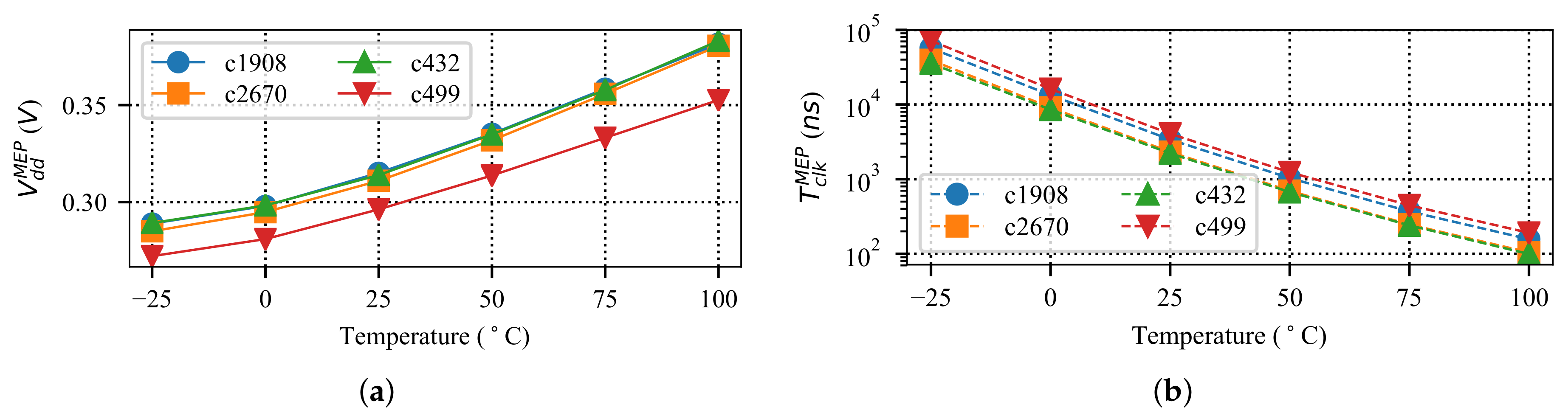
Process, Voltage, and Temperature Variation in NTC
2.2. NTC Challenges
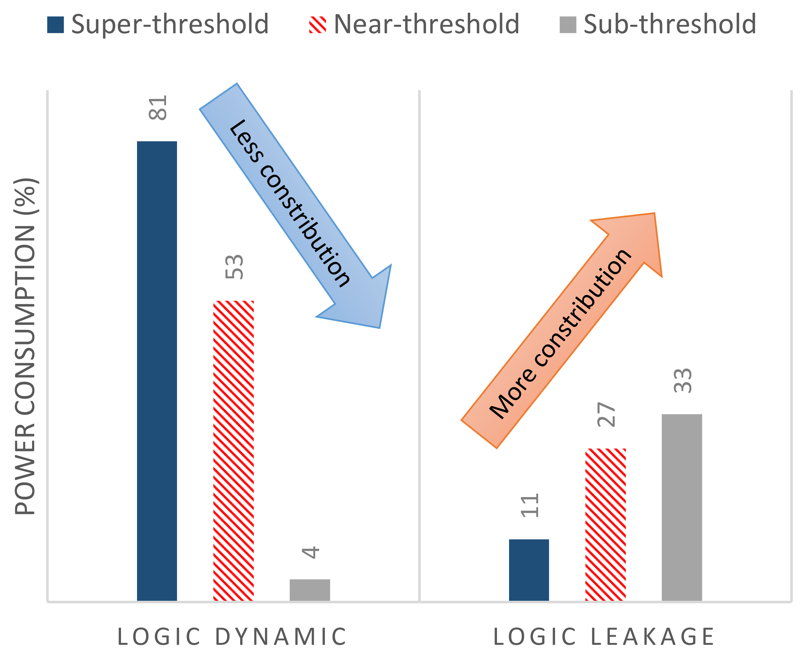
2.2.1. Reliability
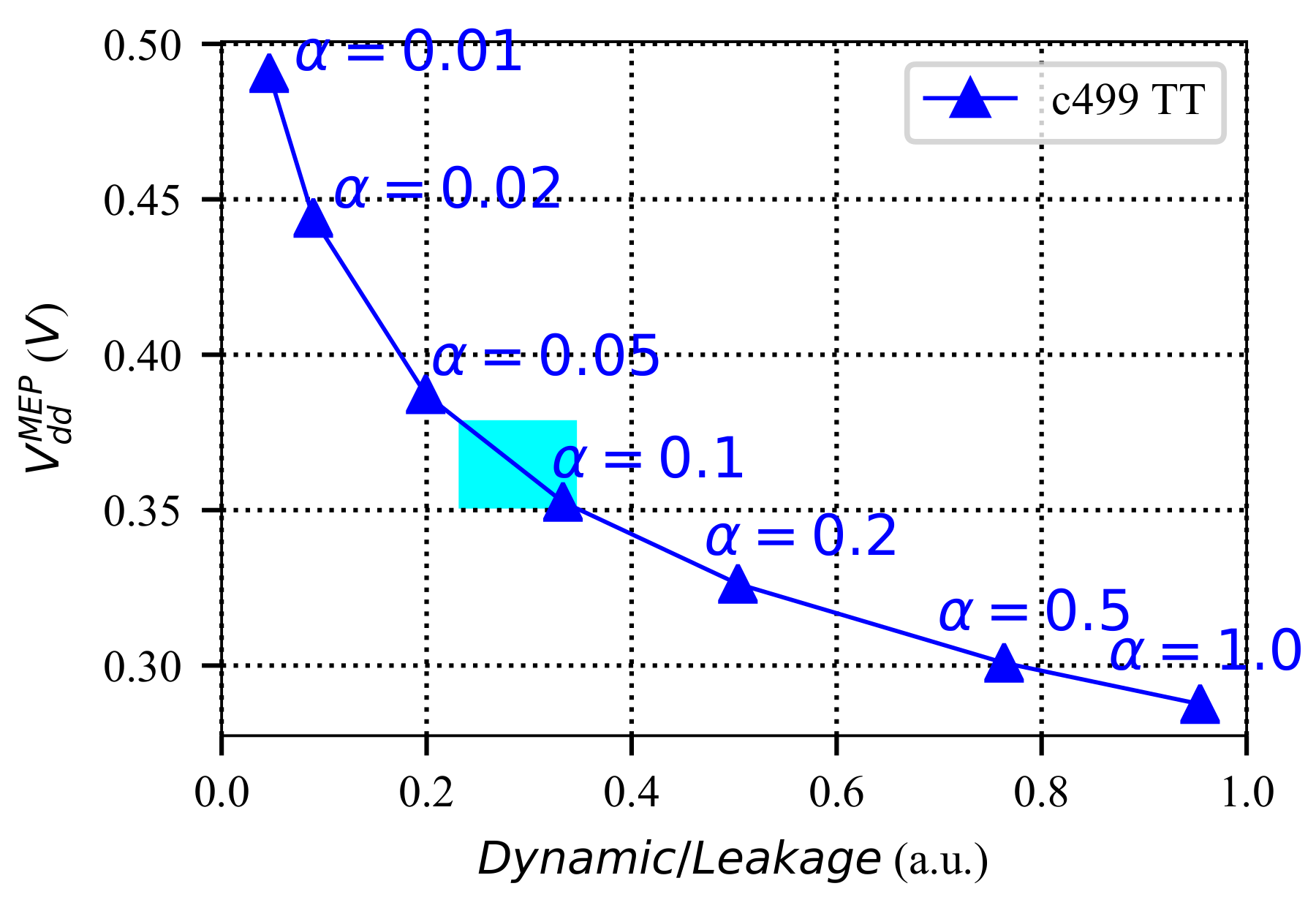
2.2.2. Energy Efficiency
2.2.3. Wide-Voltage Resiliency
2.2.4. Other Challenges
3. Related Work
- Design flow and methodology optimization: Due to high integration and the complexity associated with circuit design in modern technologies, Electronic Design Automation (EDA) tools are extensively used to enable circuit design and optimization. Hence, efforts have been focused on improving the EDA tools for NTC. Kaul et al. [33] provided a list of challenges for NTC circuit design, from device modeling to test, and desired design technologies. Recent works have addressed some of the NTC challenges in device modeling [43,72], variation modeling [40,73,74], synthesis [75], leakage power management [75,76], and system-level modeling [77]. There are still major shortcomings in variation-aware library characterization, verification, and testing.
- Design optimization for NTC: Various methods have been proposed to improve the design for NTC, from device-level to architecture-level. At circuit-level, robust standard cell libraries [26], memories [54,56,57,58] and flip-flops [27,33] are optimized for NTC. Level shifter designs have been vastly studied for interfacing between different voltage islands [60], and clock networks are redesigned for low-voltage operation [73]. Additionally, timing error correction methods such as [49,78,79] can be used to mitigate timing variations at runtime. At architecture-level, caches [80], processor pipeline [81,82,83,84] and ISA [85] can be optimized, and other leakage power reduction methods are also investigated [26]. However, there are still many opportunities for cross-layer design optimization.
- Runtime optimization and tuning: Since the MEP is dependent on process and runtime variations, runtime optimization and tuning could be required depending on the running application and the operating environment. Therefore, various runtime tuning methods have been studied, mostly based on a closed-loop hardware-implemented monitoring circuit. It is proposed by many researchers to measure the circuit power online and take actions to maximize the energy efficiency by adapting the supply voltage in a closed-loop feedback [86,87,88,89,90]. Supply voltage and threshold voltage tuning is also recommended to balance the speed of different cores [33,74,91]. However, closed-loop adaptation techniques are associated with additional circuitry for measuring the circuit power and applying the adaptation strategies, which may be too costly for NTC circuits. Therefore, low-cost adaptation methods are highly desirable for NTC.
- Wide-voltage reliability challenges: The impact of aging and supply voltage fluctuation (due to internal activity) is negligible in the NTV region due to low electric field, low current density, and low power consumption; however, operating over a wide-voltage range, from the near-threshold region to the super-threshold region may be required to satisfy performance constraints. In this case, aging phenomena affect the circuit in the super-threshold voltage region, which deteriorates the reliability. Therefore, it is necessary to address such aging challenges when applicable.
4. Cross-Layer Data Path Optimization
4.1. Overview
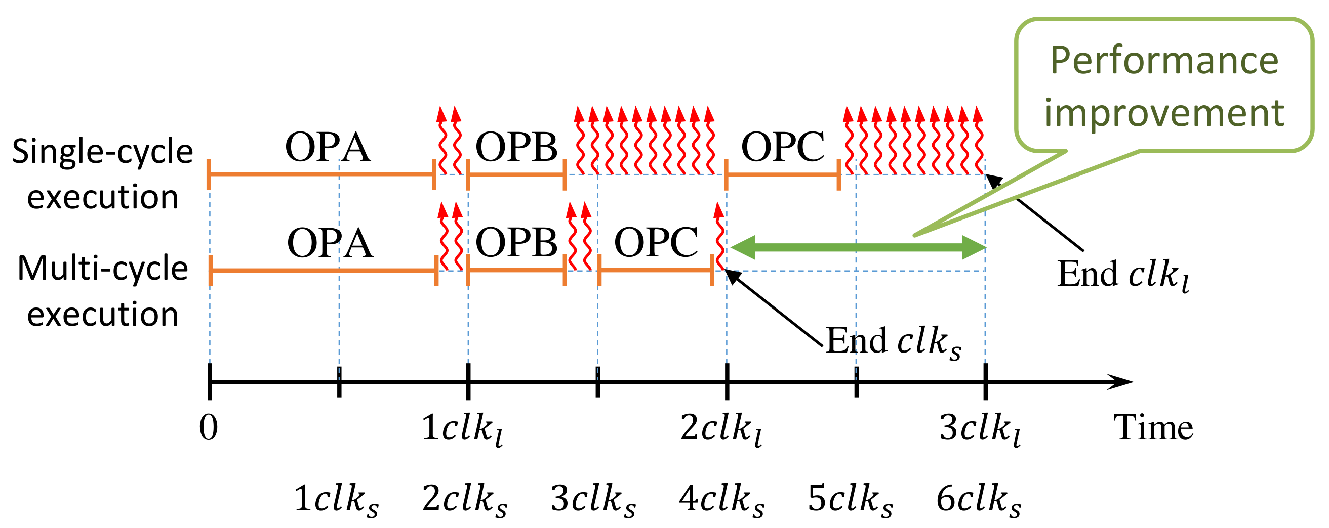
4.2. Instruction Multi-Cycling
- We classify the instructions into slow (with little timing slack) and fast (with large timing slack), based on the time required to execute the instructions. The slow instructions are executed in multiple clock cycles, to reduce the leakage power while executing fast instructions within one clock cycle.
- Contrary to the super-threshold regime, we use relaxed timing constraints for the synthesis of functional units in the NTV region. While this increases the delay of the most critical path, it avoids that all instructions have similar delays and belong to the same category. By that means, the scheme of point 1 is much more efficient.
- Finally, the clock period is not only set according to points 1 and 2 but also by considering the sensitivity of the functional unit to variations. As a result, it is possible to co-optimize energy, performance, and reliability.
- In order to reduce the number of “slow” multi-cycle operations, we propose to employ instruction- and compiler-level optimization approaches to replace some of these instructions in the code with fast single-cycle instructions, which further improves energy and performance.
4.2.1. Energy Improvement through Instruction Multi-Cycling
4.2.2. Logic Synthesis for NTV Region
4.2.3. High-Level Optimization Techniques
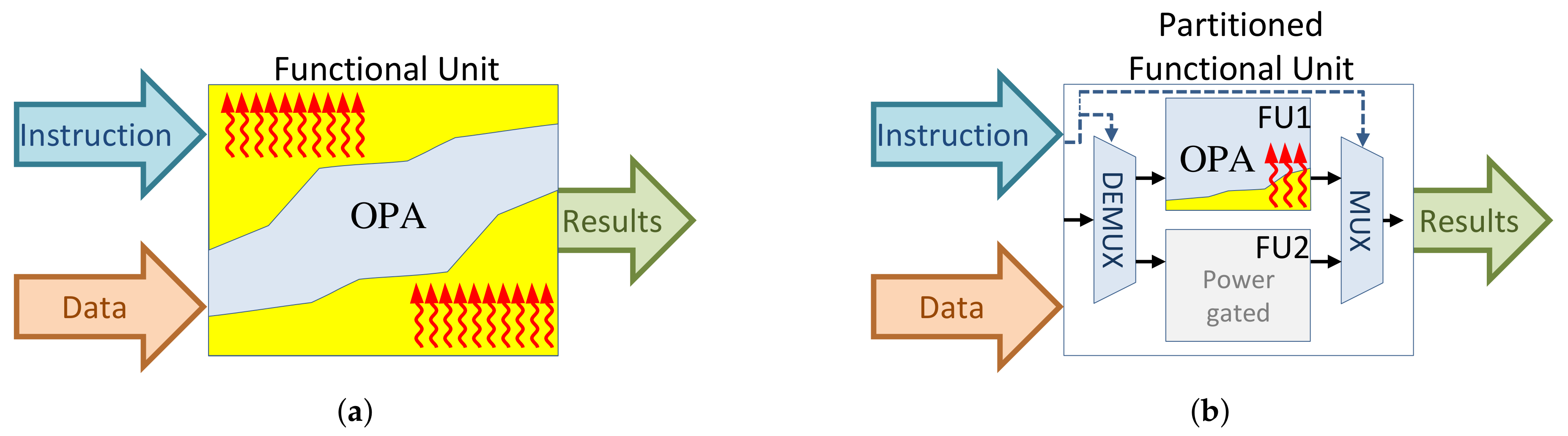
4.3. Functional Unit Partitioning
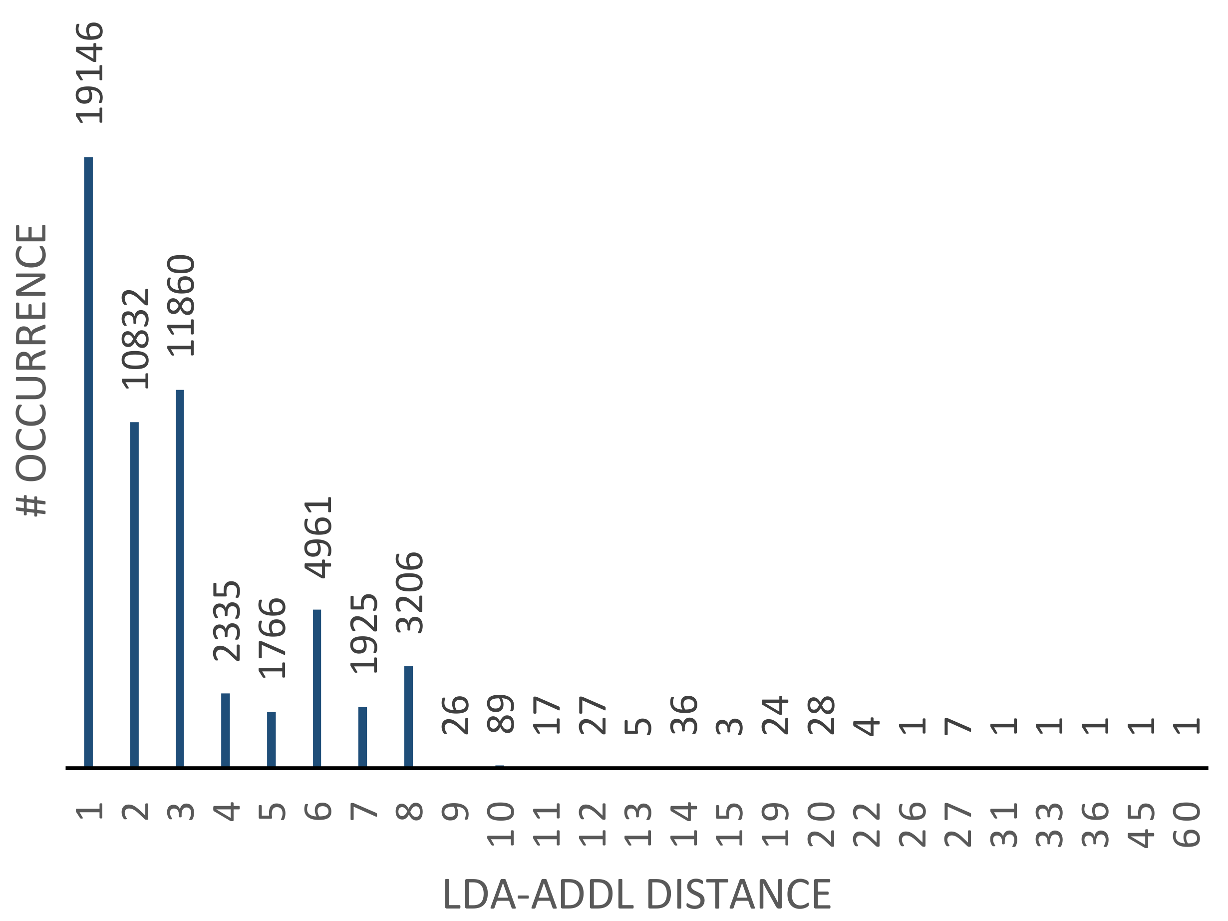
- We characterize the instruction flow of representative workloads and analyze the instruction stream in order to obtain instructions’ utilization frequency and temporal distance.
- The instructions are then partitioned into several groups according to the metrics extracted from the instruction stream analysis as well as the inherent similarity of the instruction.
- Each set of instructions residing in the same partition will be implemented by a dedicated functional unit, and they form a complete functional unit altogether.
- To reduce the leakage power, only the functional unit corresponding to the running instruction partition is activated while other units are power-gated.
4.3.1. Instruction Pattern Analysis
4.3.2. Instruction Clustering Problem Definition
4.3.3. Fine-Grained Power-Gating Prediction
5. Results and Discussion
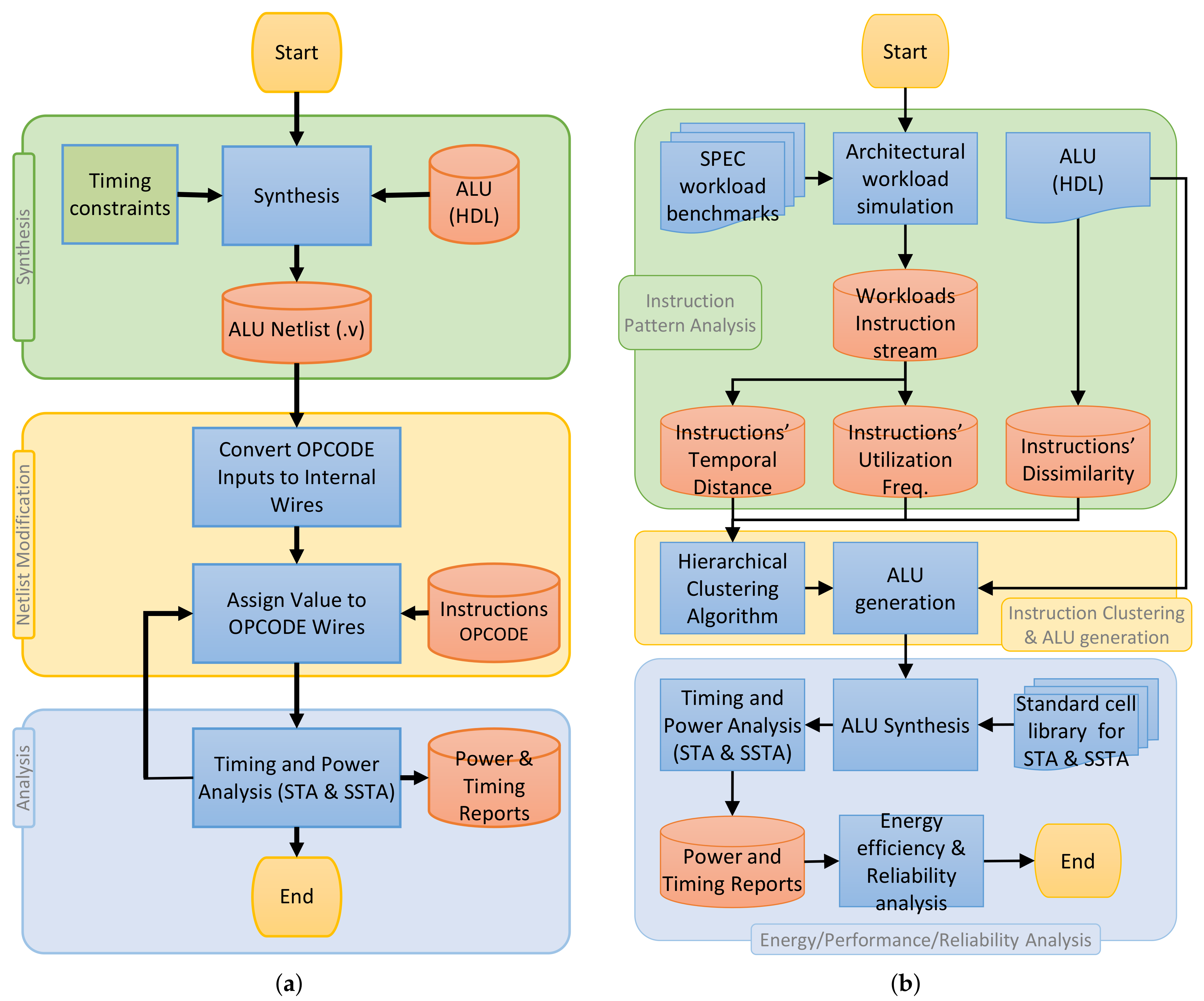
5.1. Implementation Flow
5.1.1. Input Vector Dependent Timing and Power Analysis
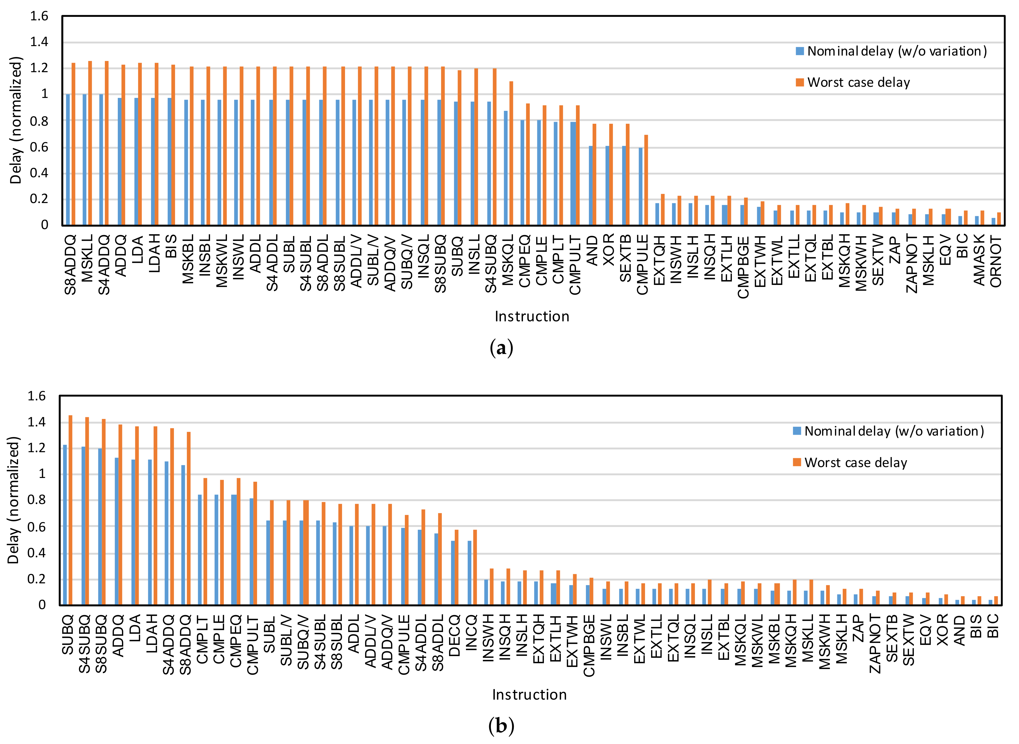
- Synthesis: The synthesis step of Figure 11a is executed with timing constraints to obtain the gate level netlist of the synthesized ALU.
- Netlist modification: The synthesized netlists of the ALUs are modified such that the OPCODE input signals that determine the instruction to be executed are changed to internal wires. For each instruction, the OPCODE signals are assigned to associated values inside the Verilog netlist. This will effectively deactivate the rest of the instruction paths in the ALU and force the STA tool to evaluate only the paths associated with the execution of the given instruction. This is because the rest of the paths (which belong to other instructions) are deactivated, and any change in the output pins of the ALU is only due to the paths belonging to the given instruction.
- Timing and power analysis: The timing and power analyses are performed on the modified netlists, and the delay of the instructions considering the variation as well as the dynamic power and the leakage power for each instruction are extracted.
5.1.2. Functional Unit Partitioning Flow
- Instruction Pattern Analysis: In this step, the instruction stream extracted from running representative workloads are analyzed to extract instruction temporal distance and utilization frequency. Instruction dissimilarity is also defined based on the field knowledge about the implementation of logic units.
- Instruction Clustering and ALU generation: With the help of the information collected from the previous step, instructions are grouped into n clusters, and each cluster is implemented as a new ALU. Moreover, all the partitioned ALUs are combined with a circuit for multiplexing their outputs to form a union ALU, as shown in Figure 7b.
- Energy, Performance and Reliability Analysis: The union ALU generated from the previous step is evaluated in terms of timing and performance, and finally, its reliability is evaluated when it is used instead of the original ALU.
5.2. Reliability Analysis
5.3. Simulation Setup
5.4. ALU Multi-Cycling Results
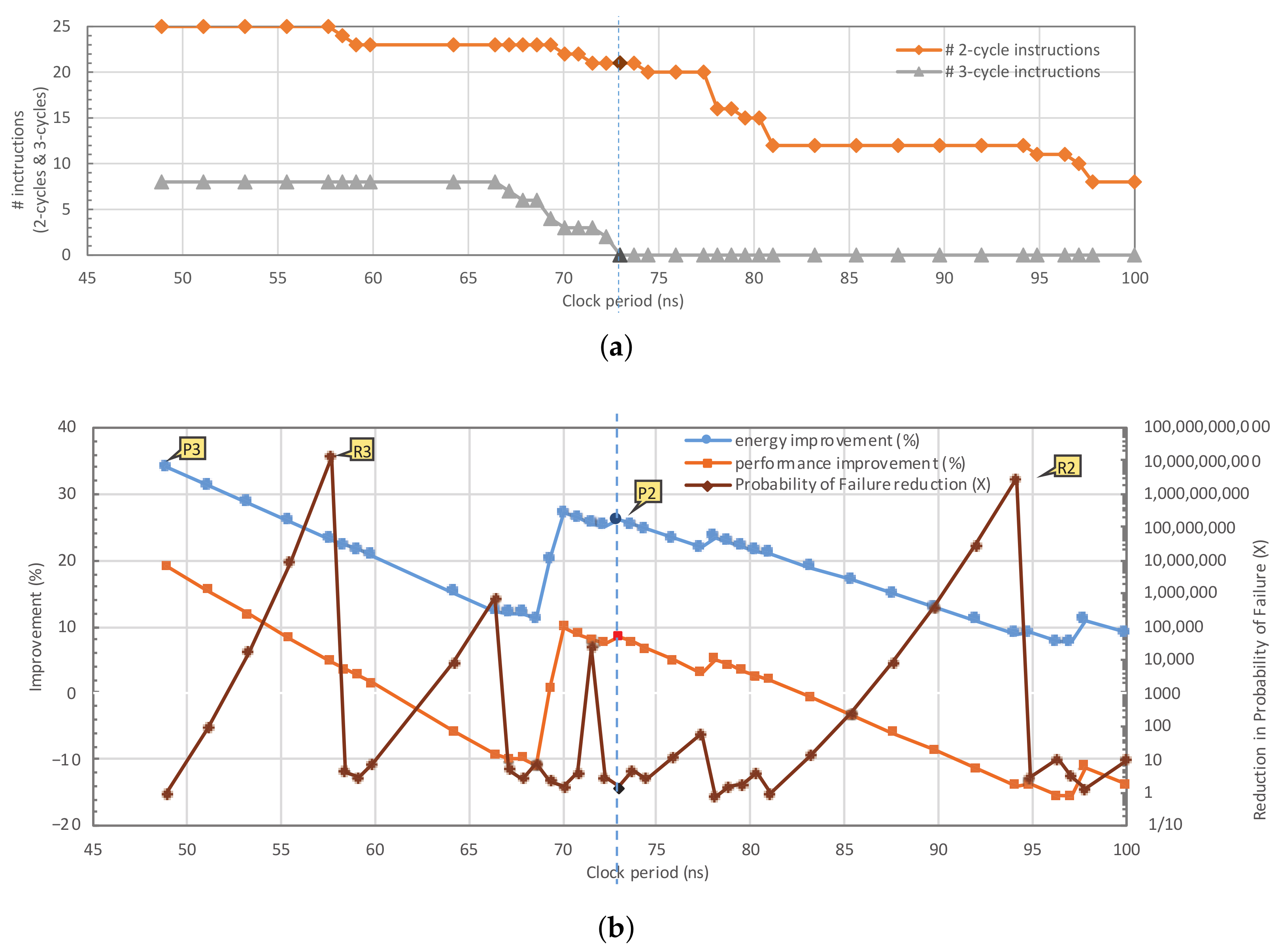
5.4.1. Multi-Cycling Improvement
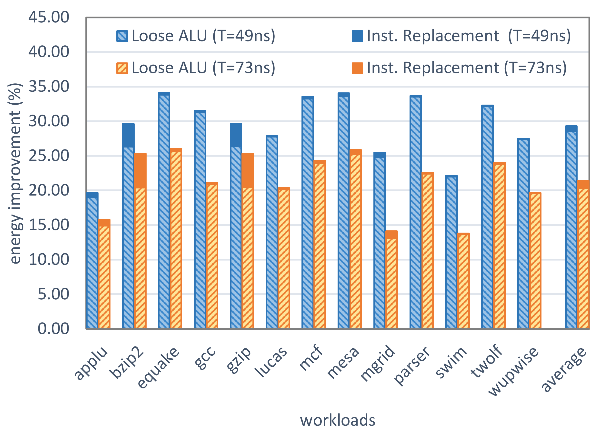
5.4.2. Impact of Workload on the Improvement Ratio
5.4.3. High-Level Optimization Improvements
5.4.4. Energy/Performance/Reliability Trade-Off
5.4.5. Discussion
5.5. Functional Unit Partitioning Results
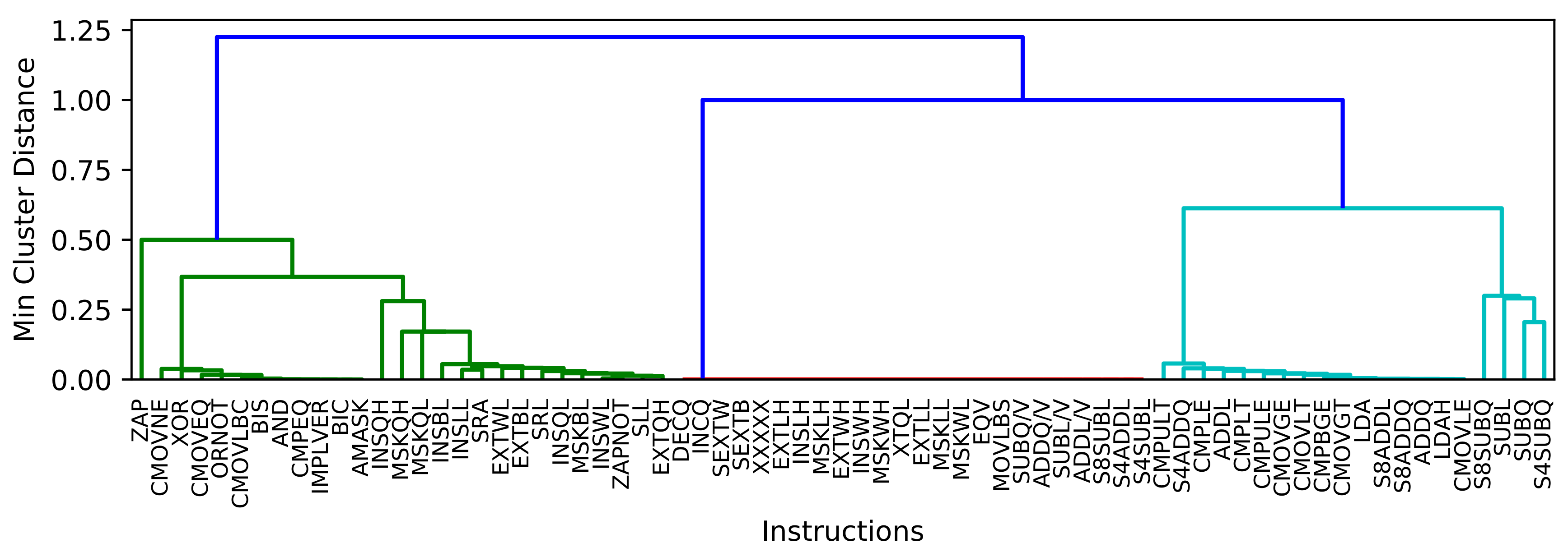
5.5.1. Clustering Results
5.5.2. Circuit-Level Results
5.5.3. Performance and Reliability Trade-Off
6. Summary
Author Contributions
Funding
Conflicts of Interest
References
- Moore, G. Cramming more components onto integrated circuits. Electronics 1965, 38, 114–117. [Google Scholar] [CrossRef]
- Moore, G.E. Progress in digital integrated electronics. In Proceedings of the International Electron Devices Meeting (IEDM), Washington, DC, USA, 1–3 December 1975; Volume 21, pp. 11–13. [Google Scholar]
- Brock, D.C.; Moore, G.E. Understanding Moore’s Law: Four Decades of Innovation; Chemical Heritage Foundation: Philadelphia, PA, USA, 2006. [Google Scholar]
- Borkar, S. Design challenges of technology scaling. IEEE Micro 1999, 19, 23–29. [Google Scholar] [CrossRef]
- Bohr, M. The new era of scaling in an SoC world. In Proceedings of the International Solid-State Circuits Conference (ISSCC), San Francisco, CA, USA, 8–12 February 2009; pp. 23–28. [Google Scholar]
- International Technology Roadmap for Semiconductors (ITRS). Available online: http://www.itrs2.net (accessed on 17 August 2020).
- International Roadmap for Devices and Systems (IRDS). Available online: https://irds.ieee.org (accessed on 17 August 2020).
- Dennard, R.H.; Gaensslen, F.H.; Rideout, V.L.; Bassous, E.; LeBlanc, A.R. Design of ion-implanted MOSFET’s with very small physical dimensions. IEEE J. Solid State Circuits 1974, 9, 256–268. [Google Scholar] [CrossRef] [Green Version]
- Bohr, M. A 30 year retrospective on Dennard’s MOSFET scaling paper. IEEE Solid State Circuits Soc. Newsl. 2007, 12, 11–13. [Google Scholar] [CrossRef]
- Borkar, S.; Chien, A.A. The Future of Microprocessors. Commun. ACM 2011, 54, 67–77. [Google Scholar] [CrossRef]
- Esmaeilzadeh, H.; Blem, E.; Amant, R.S.; Sankaralingam, K.; Burger, D. Dark silicon and the end of multicore scaling. In Proceedings of the International Symposium on Computer Architecture (ISCA), San Jose, CA, USA, 4–8 June 2011; pp. 365–376. [Google Scholar]
- Chang, L.; Frank, D.J.; Montoye, R.K.; Koester, S.J.; Ji, B.L.; Coteus, P.W.; Dennard, R.H.; Haensch, W. Practical Strategies for Power-Efficient Computing Technologies. Proc. IEEE 2010, 98, 215–236. [Google Scholar] [CrossRef]
- Esmaeilzadeh, H.; Blem, E.; St. Amant, R.; Sankaralingam, K.; Burger, D. Power Limitations and Dark Silicon Challenge the Future of Multicore. ACM Trans. Comput. Syst. (TOCS) 2012, 30, 1–27. [Google Scholar] [CrossRef]
- Evans, D. The Internet of Things: How the Next Evolution of the Internet Is Changing Everything. In CISCO White Paper; Cisco IBSG: San Jose, CA, USA, 2011; pp. 1–11. [Google Scholar]
- Ericsson, A. Enabling the internet of things. In Ericsson Mobility Report: On the Pulse of the Networked Society; Ericsson AB: Stockholm, Sweden, 2015; p. 10. [Google Scholar]
- Middleton, P. Forecast Analysis: Internet of Things—Endpoints, Worldwide, 2016 Update. 2017. Available online: https://www.gartner.com/en/documents/3841268/forecast-analysis-internet-of-things-endpoints-worldwide (accessed on 2 November 2020).
- Avgerinou, M.; Bertoldi, P.; Castellazzi, L. Trends in data centre energy consumption under the European code of conduct for data centre energy efficiency. Energies 2017, 10, 1470. [Google Scholar] [CrossRef]
- Pedram, M. Power minimization in IC design: Principles and applications. ACM TRansactions Des. Autom. Electron. Syst. (TODAES) 1996, 1, 3–56. [Google Scholar] [CrossRef]
- Pedram, M. Low power design methodologies and techniques: An overview. Microprocess. Rep. 1999, 486, 66. [Google Scholar]
- Tiwari, V.; Singh, D.; Rajgopal, S.; Mehta, G.; Patel, R.; Baez, F. Reducing Power in High-performance Microprocessors. In Proceedings of the Design Automation Conference (DAC), San Francisco, CA, USA, 15–19 June 1998; pp. 732–737. [Google Scholar]
- Semeraro, G.; Magklis, G.; Balasubramonian, R.; Albonesi, D.H.; Dwarkadas, S.; Scott, M.L. Energy-efficient processor design using multiple clock domains with dynamic voltage and frequency scaling. In Proceedings of the International Symposium on High-Performance Computer Architecture (HPCA), Cambridge, MA, USA, 2–6 February 2002; pp. 29–40. [Google Scholar]
- Burd, T.D.; Pering, T.A.; Stratakos, A.J.; Brodersen, R.W. A dynamic voltage scaled microprocessor system. IEEE J. Solid State Circuits 2000, 35, 1571–1580. [Google Scholar] [CrossRef]
- Chandrakasan, A.P.; Sheng, S.; Brodersen, R.W. Low-power CMOS digital design. IEEE J. Solid State Circuits 1992, 27, 473–484. [Google Scholar] [CrossRef] [Green Version]
- Soeleman, H.; Roy, K.; Paul, B.C. Robust subthreshold logic for ultra-low power operation. IEEE Trans. Very Large Scale Integr. (VLSI) Syst. 2001, 9, 90–99. [Google Scholar] [CrossRef]
- Gonzalez, R.; Gordon, B.M.; Horowitz, M.A. Supply and threshold voltage scaling for low power CMOS. IEEE J. Solid State Circuits 1997, 32, 1210–1216. [Google Scholar] [CrossRef] [Green Version]
- Jain, S.; Khare, S.; Yada, S.; Ambili, V.; Salihundam, P.; Ramani, S.; Muthukumar, S.; Srinivasan, M.; Kumar, A.; Gb, S.K.; et al. A 280 mV-to-1.2 V wide-operating-range IA-32 processor in 32 nm CMOS. In Proceedings of the International Solid-State Circuits Conference (ISSCC), San Francisco, CA, USA, 19–23 February 2012; pp. 66–68. [Google Scholar]
- Dreslinski, R.G.; Wieckowski, M.; Blaauw, D.; Sylvester, D.; Mudge, T. Near-threshold computing: Reclaiming moore’s law through energy efficient integrated circuits. Proc. IEEE 2010, 98, 253–266. [Google Scholar] [CrossRef]
- Kaul, H.; Anders, M.A.; Mathew, S.K.; Hsu, S.K.; Agarwal, A.; Krishnamurthy, R.K.; Borkar, S. A 320 mv 56 μw 411 gops/watt ultra-low voltage motion estimation accelerator in 65 nm cmos. IEEE J. Solid State Circuits 2009, 44, 107–114. [Google Scholar] [CrossRef]
- Pahlevan, A.; Picorel, J.; Zarandi, A.P.; Rossi, D.; Zapater, M.; Bartolini, A.; Del Valle, P.G.; Atienza, D.; Benini, L.; Falsafi, B. Towards near-threshold server processors. In Proceedings of the Design, Automation & Test in Europe Conference (DATE), Dresden, Germany, 14–18 March 2016; pp. 7–12. [Google Scholar]
- Dreslinski, R., Jr. Near Threshold Computing: From Single Core to Many-Core Energy Efficient Architectures. Ph.D. Thesis, University of Michigan, Ann Arbor, MI, USA, 2011. [Google Scholar]
- De, V. Fine-grain power management in manycore processor and System-on-Chip (SoC) designs. In Proceedings of the International Conference on Computer-Aided Design (ICCAD), Austin, TX, USA, 2–6 November 2015; pp. 159–164. [Google Scholar]
- Zhai, B.; Dreslinski, R.G.; Blaauw, D.; Mudge, T.; Sylvester, D. Energy Efficient Near-threshold Chip Multi-processing. In Proceedings of the International Symposium on Low Power Electronics and Design (ISLPED), Portland, OR, USA, 27–29 August 2007; pp. 32–37. [Google Scholar]
- Kaul, H.; Anders, M.; Hsu, S.; Agarwal, A.; Krishnamurthy, R.; Borkar, S. Near-threshold voltage (NTV) design: Opportunities and challenges. In Proceedings of the Design Automation Conference (DAC), San Francisco, CA, USA, 3–7 June 2012; pp. 1153–1158. [Google Scholar]
- Alidina, M.; Monteiro, J.; Devadas, S.; Ghosh, A.; Papaefthymiou, M. Precomputation-based sequential logic optimization for low power. IEEE Trans. Very Large Scale Integr. (VLSI) Syst. 1994, 2, 426–436. [Google Scholar] [CrossRef] [Green Version]
- Benini, L.; De Micheli, G.; Macii, E. Designing low-power circuits: Practical recipes. IEEE Circuits Syst. Mag. 2001, 1, 6–25. [Google Scholar] [CrossRef]
- Wei, L.; Chen, Z.; Johnson, M.; Roy, K.; De, V. Design and optimization of low voltage high performance dual threshold CMOS circuits. In Proceedings of the Design Automation Conference (DAC), San Francisco, CA, USA, 15–19 June 1998; pp. 489–494. [Google Scholar]
- Fujiwara, F.B. A Neutral Netlist of 10 Combinational Benchmark Circuits. In Proceedings of the International Symposium on Circuits and Systems (ISCAS), Kyoto, Japan, 5–7 June 1985; pp. 695–698. [Google Scholar]
- Brglez, F.; Pownall, P.; Hum, R. Accelerated ATPG and fault grading via testability analysis. In Proceedings of the International Symposium on Circuits and Systems (ISCAS), Kyoto, Japan, 5–7 June 1985; pp. 695–698. [Google Scholar]
- Sakurai, T.; Newton, A.R. Alpha-power law MOSFET model and its applications to CMOS inverter delay and other formulas. IEEE J. Solid State Circuits 1990, 25, 584–594. [Google Scholar] [CrossRef] [Green Version]
- Markovic, D.; Wang, C.C.; Alarcon, L.P.; Liu, T.; Rabaey, J.M. Ultralow-Power Design in Near-Threshold Region. Proc. IEEE 2010, 98, 237–252. [Google Scholar] [CrossRef]
- Enz, C.C.; Krummenacher, F.; Vittoz, E.A. An analytical MOS transistor model valid in all regions of operation and dedicated to low-voltage and low-current applications. Analog. Integr. Circuits Signal Process. 1995, 8, 83–114. [Google Scholar] [CrossRef]
- Bucher, M.; Bazigos, A.; Krummenacher, F.; Sallese, J.M.; Enz, C. EKV3. 0: An advanced charge based MOS transistor model. A design-oriented MOS transistor compact model. In Transistor Level Modeling for Analog/RF IC Design; Springer: Berlin/Heidelberg, Germany, 2006; pp. 67–95. [Google Scholar]
- Keller, S.; Harris, D.M.; Martin, A.J. A compact transregional model for digital CMOS circuits operating near threshold. IEEE Trans. Very Large Scale Integr. (VLSI) Syst. 2014, 22, 2041–2053. [Google Scholar] [CrossRef]
- Drego, N.; Chandrakasan, A.; Boning, D. Lack of spatial correlation in MOSFET threshold voltage variation and implications for voltage scaling. IEEE Trans. Semicond. Manuf. 2009, 22, 245–255. [Google Scholar] [CrossRef]
- Hanson, S.; Zhai, B.; Bernstein, K.; Blaauw, D.; Bryant, A.; Chang, L.; Das, K.K.; Haensch, W.; Nowak, E.J.; Sylvester, D.M. Ultralow-voltage, minimum-energy CMOS. IBM J. Res. Dev. 2006, 50, 469–490. [Google Scholar] [CrossRef] [Green Version]
- Kiamehr, S.; Ebrahimi, M.; Golanbari, M.S.; Tahoori, M.B. Temperature-aware dynamic voltage scaling to improve energy efficiency of near-threshold computing. IEEE Trans. Very Large Scale Integr. (VLSI) Syst. 2017, 25, 2017–2026. [Google Scholar] [CrossRef]
- Krishnamurthy, R.K.; Himanshu, K. Ultra-low voltage technologies for energy-efficient special-purpose hardware accelerators. Intel Technol. J. 2009, 13, 102–117. [Google Scholar]
- Bowman, K.; Tschanz, J.; Wilkerson, C.; Lu, S.L.; Karnik, T.; De, V.; Borkar, S. Circuit techniques for dynamic variation tolerance. In Proceedings of the Design Automation Conference (DAC), San Francisco, CA, USA, 26–31 July 2009; pp. 4–7. [Google Scholar]
- Ernst, D.; Das, S.; Lee, S.; Blaauw, D.; Austin, T.; Mudge, T.; Kim, N.S.; Flautner, K. Razor: Circuit-level correction of timing errors for low-power operation. IEEE Micro 2004, 24, 10–20. [Google Scholar] [CrossRef]
- Greskamp, B.; Torrellas, J. Paceline: Improving single-thread performance in nanoscale CMPs through core overclocking. In Proceedings of the International Conference on Parallel Architecture and Compilation Techniques (IEEE Computer Society), Brasov, Romania, 15–19 September 2007; pp. 213–224. [Google Scholar]
- Ramasubramanian, S.G.; Venkataramani, S.; Parandhaman, A.; Raghunathan, A. Relax-and-retime: A methodology for energy-efficient recovery based design. In Proceedings of the Design Automation Conference (DAC), Austin, TX, USA, 2–6 June 2013; p. 111. [Google Scholar]
- Liu, Y.; Ye, R.; Yuan, F.; Kumar, R.; Xu, Q. On logic synthesis for timing speculation. In Proceedings of the International Conference on Computer-Aided Design (ICCAD), San Jose, CA, USA, 5–8 November 2012; pp. 591–596. [Google Scholar]
- Golanbari, M.S.; Kiamehr, S.; Tahoori, M.B. Hold-time Violation Analysis and Fixing in Near-Threshold Region. In Proceedings of the International Workshop on Power and Timing Modeling, Optimization and Simulation (PATMOS), Bremen, Germany, 21–23 September 2016. [Google Scholar]
- Zhai, B.; Hanson, S.; Blaauw, D.; Sylvester, D. A variation-tolerant sub-200 mV 6-T subthreshold SRAM. IEEE J. Solid State Circuits 2008, 43, 2338. [Google Scholar] [CrossRef]
- Chang, L.; Montoye, R.K.; Nakamura, Y.; Batson, K.A.; Eickemeyer, R.J.; Dennard, R.H.; Haensch, W.; Jamsek, D. An 8T-SRAM for variability tolerance and low-voltage operation in high-performance caches. IEEE J. Solid State Circuits 2008, 43, 956–963. [Google Scholar] [CrossRef]
- Chang, L.; Fried, D.M.; Hergenrother, J.; Sleight, J.W.; Dennard, R.H.; Montoye, R.K.; Sekaric, L.; McNab, S.J.; Topol, A.W.; Adams, C.D.; et al. Stable SRAM cell design for the 32 nm node and beyond. In Symposium on VLSI Technology; IEEE: Piscataway, NJ, USA, 2005; pp. 128–129. [Google Scholar]
- Kulkarni, J.P.; Kim, K.; Roy, K. A 160 mV, fully differential, robust schmitt trigger based sub-threshold SRAM. In Proceedings of the International Symposium on Low Power Electronics and Design (ISLPED), Portland, OR, USA, 27–29 August 2007; pp. 171–176. [Google Scholar]
- Calhoun, B.H.; Chandrakasan, A. A 256kb sub-threshold SRAM in 65nm CMOS. In Proceedings of the International Solid-State Circuits Conference (ISSCC), San Francisco, CA, USA, 6–9 February 2006; pp. 2592–2601. [Google Scholar]
- Hu, J.; Yu, X. Low voltage and low power pulse flip-flops in nanometer CMOS processes. Curr. Nanosci. 2012, 8, 102–107. [Google Scholar] [CrossRef]
- Pinckney, N.; Blaauw, D.; Sylvester, D. Low-power near-threshold design: Techniques to improve energy efficiency. IEEE Solid State Circuits Mag. 2015, 7, 49–57. [Google Scholar] [CrossRef]
- Fuketa, H.; Hirairi, K.; Yasufuku, T.; Takamiya, M.; Nomura, M.; Shinohara, H.; Sakurai, T. 12.7-times energy efficiency increase of 16-bit integer unit by power supply voltage (V DD) scaling from 1.2 V to 310 mV enabled by contention-less flip-flops (CLFF) and separated V DD between flip-flops and combinational logics. In Proceedings of the International Symposium on Low Power Electronics and Design (ISLPED), Fukuoka, Japan, 1–3 August 2011; pp. 163–168. [Google Scholar]
- Chandra, V.; Aitken, R. Impact of technology and voltage scaling on the soft error susceptibility in nanoscale CMOS. In Proceedings of the IEEE International Symposium on Defect and Fault Tolerance of VLSI Systems, Boston, MA, USA, 1–3 October 2008; pp. 114–122. [Google Scholar]
- Cannon, E.H.; Reinhardt, D.D.; Gordon, M.S.; Makowenskyj, P.S. SRAM SER in 90, 130 and 180 nm bulk and SOI technologies. In Proceedings of the IEEE International Reliability Physics Symposium Proceedings (IRPS), Phoenix, AZ, USA, 25–29 April 2004; pp. 300–304. [Google Scholar]
- Hazucha, P.; Karnik, T.; Walstra, S.; Bloechel, B.A.; Tschanz, J.W.; Maiz, J.; Soumyanath, K.; Dermer, G.E.; Narendra, S.; De, V.; et al. Measurements and analysis of SER-tolerant latch in a 90-nm dual-V/sub T/CMOS process. IEEE J. Solid State Circuits 2004, 39, 1536–1543. [Google Scholar] [CrossRef]
- Naseer, R.; Draper, J. DF-DICE: A scalable solution for soft error tolerant circuit design. In Proceedings of the International Symposium on Circuits and System (ISCAS), Island of Kos, Greece, 21–24 May 2006; pp. 3890–3893. [Google Scholar]
- Zhang, M.; Mitra, S.; Mak, T.; Seifert, N.; Wang, N.J.; Shi, Q.; Kim, K.S.; Shanbhag, N.R.; Patel, S.J. Sequential element design with built-in soft error resilience. IEEE Trans. Very Large Scale Integr. (VLSI) Syst. 2006, 14, 1368–1378. [Google Scholar] [CrossRef]
- Zhou, Q.; Mohanram, K. Transistor sizing for radiation hardening. In Proceedings of the International Reliability Physics Symposium (IRPS), Phoenix, AZ, USA, 25–29 April 2004; pp. 310–315. [Google Scholar]
- Ebrahimi, M.; Rao, P.M.B.; Seyyedi, R.; Tahoori, M.B. Low-cost multiple bit upset correction in SRAM-based FPGA configuration frames. IEEE Trans. Very Large Scale Integr. (VLSI) Syst. 2016, 24, 932–943. [Google Scholar] [CrossRef]
- Chang, I.J.; Kim, J.J.; Park, S.P.; Roy, K. A 32 kb 10T sub-threshold SRAM array with bit-interleaving and differential read scheme in 90 nm CMOS. IEEE J. Solid State Circuits 2009, 44, 650–658. [Google Scholar] [CrossRef] [Green Version]
- Fu, X.; Li, T.; Fortes, J.A.B. Soft error vulnerability aware process variation mitigation. In Proceedings of the International Symposium on High Performance Computer Architecture (HPCA), Raleigh, NC, USA, 14–18 February 2009; pp. 93–104. [Google Scholar]
- Golanbari, M.S. Design and Optimization for Resilient Energy Efficient Computing. Ph.D. Thesis, Karlsruher Institut für Technologie (KIT), Karlsruhe, Germany, 2019. [CrossRef]
- Markov, S.; Zain, A.S.M.; Cheng, B.; Asenov, A. Statistical variability in scaled generations of n-channel UTB-FD-SOI MOSFETs under the influence of RDF, LER, OTF and MGG. In Proceedings of the IEEE International SOI Conference (SOI), Napa, CA, USA, 1–4 October 2012; pp. 1–2. [Google Scholar]
- Seok, M.; Chen, G.; Hanson, S.; Wieckowski, M.; Blaauw, D.; Sylvester, D. CAS-FEST 2010: Mitigating variability in near-threshold computing. IEEE J. Emerg. Sel. Top. Circuits Syst. 2011, 1, 42–49. [Google Scholar] [CrossRef] [Green Version]
- Hanson, S.; Zhai, B.; Seok, M.; Cline, B.; Zhou, K.; Singhal, M.; Minuth, M.; Olson, J.; Nazhandali, L.; Austin, T.; et al. Performance and variability optimization strategies in a sub-200 mV, 3.5 pJ/inst, 11nW subthreshold processor. In IEEE Symposium on VLSI Circuits; IEEE: Piscataway, NJ, USA, 2007; pp. 152–153. [Google Scholar]
- Kakoee, M.R.; Sathanur, A.; Pullini, A.; Huisken, J.; Benini, L. Automatic synthesis of near-threshold circuits with fine-grained performance tunability. In Proceedings of the International Symposium on Low Power Electronics and Design (ISLPED), Austin, TX, USA, 18–20 August 2010; pp. 401–406. [Google Scholar]
- Myers, J.; Savanth, A.; Gaddh, R.; Howard, D.; Prabhat, P.; Flynn, D. A subthreshold ARM cortex-M0+ subsystem in 65 nm CMOS for WSN applications with 14 power domains, 10T SRAM, and integrated voltage regulator. IEEE J. Solid State Circuits 2016, 51, 31–44. [Google Scholar]
- Karpuzcu, U.R.; Kim, N.S.; Torrellas, J. Coping with parametric variation at near-threshold voltages. IEEE Micro 2013, 33, 6–14. [Google Scholar] [CrossRef]
- Kim, S.; Kwon, I.; Fick, D.; Kim, M.; Chen, Y.P.; Sylvester, D. Razor-lite: A side-channel error-detection register for timing-margin recovery in 45nm SOI CMOS. In Proceedings of the International Solid-State Circuits Conference (ISSCC), San Francisco, CA, USA, 17–21 February 2013; pp. 264–265. [Google Scholar]
- Austin, T.; Bertacco, V.; Blaauw, D.; Mudge, T. Opportunities and challenges for better than worst-case design. In Proceedings of the Asia and South Pacific Design Automation Conference (ASP-DAC), Shanghai, China, 18–21 January 2005; pp. 2–7. [Google Scholar]
- Gebregiorgis, A.; Bishnoi, R.; Tahoori, M.B. A Comprehensive Reliability Analysis Framework for NTC Caches: A System to Device Approach. IEEE Trans. Comput. Aided Des. Integr. Circuits Syst. 2018, 38, 439–452. [Google Scholar] [CrossRef]
- Zhai, B.; Pant, S.; Nazhandali, L.; Hanson, S.; Olson, J.; Reeves, A.; Minuth, M.; Helfand, R.; Austin, T.; Sylvester, D.; et al. Energy-efficient subthreshold processor design. IEEE Trans. Very Large Scale Integr. (VLSI) Syst. 2009, 17, 1127–1137. [Google Scholar] [CrossRef]
- Gebregiorgis, A.; Golanbari, M.S.; Kiamehr, S.; Oboril, F.; Tahoori, M.B. Maximizing Energy Efficiency in NTC by Variation-Aware Microprocessor Pipeline Optimization. In Proceedings of the International Symposium on Low Power Electronics and Design (ISLPED), San Francisco, CA, USA, 8–10 August 2016; pp. 272–277. [Google Scholar]
- Zhai, B.; Hanson, S.; Blaauw, D.; Sylvester, D. Analysis and mitigation of variability in subthreshold design. In Proceedings of the International Symposium on Low Power Electronics and Design (ISLPED), San Diego, CA, USA, 8–10 August 2005; pp. 20–25. [Google Scholar]
- Gebregiorgis, A.; Tahoori, M.B. Fine-Grained Energy-Constrained Microprocessor Pipeline Design. IEEE Trans. Very Large Scale Integr. (VLSI) Syst. 2018, 26, 457–469. [Google Scholar] [CrossRef]
- Nazhandali, L.; Zhai, B.; Olson, J.; Reeves, A.; Minuth, M.; Helfand, R.; Pant, S.; Austin, T.; Blaauw, D. Energy optimization of subthreshold-voltage sensor network processors. ACM Sigarch Comput. Archit. News 2005, 33, 197–207. [Google Scholar] [CrossRef]
- Ramadass, Y.K.; Chandrakasan, A.P. Minimum energy tracking loop with embedded DC–DC converter enabling ultra-low-voltage operation down to 250 mV in 65 nm CMOS. IEEE J. Solid State Circuits 2008, 43, 256–265. [Google Scholar] [CrossRef]
- Ikenaga, Y.; Nomura, M.; Nakazawa, Y.; Hagihara, Y. A circuit for determining the optimal supply voltage to minimize energy consumption in LSI circuit operations. IEEE J. Solid State Circuits 2008, 43, 911–918. [Google Scholar] [CrossRef]
- Koskinen, L.; Hiienkari, M.; Mäkipää, J.; Turnquist, M.J. Implementing minimum-energy-point systems with adaptive logic. IEEE Trans. Very Large Scale Integr. (VLSI) Syst. 2016, 24, 1247–1256. [Google Scholar] [CrossRef] [Green Version]
- Mehta, N.; Makinwa, K.A. Minimum energy point tracking for sub-threshold digital CMOS circuits using an in-situ energy sensor. In Proceedings of the International Symposium on Circuits and Systems (ISCAS), Beijing, China, 19–23 May 2013; pp. 570–573. [Google Scholar]
- Mehta, N.; Amrutur, B. Dynamic supply and threshold voltage scaling for CMOS digital circuits using in-situ power monitor. IEEE Trans. Very Large Scale Integr. (VLSI) Syst. 2012, 20, 892–901. [Google Scholar] [CrossRef]
- Wang, A.; Chandrakasan, A.P.; Kosonocky, S.V. Optimal supply and threshold scaling for subthreshold CMOS circuits. In Proceedings of the IEEE Computer Society Annual Symposium on VLSI, Pittsburgh, PA, USA, 25–26 April 2002; pp. 7–11. [Google Scholar]
- Calhoun, B.H.; Wang, A.; Chandrakasan, A. Modeling and sizing for minimum energy operation in subthreshold circuits. IEEE J. Solid State Circuits 2005, 40, 1778–1786. [Google Scholar] [CrossRef]
- Karpuzcu, U.R.; Sinkar, A.; Kim, N.S.; Torrellas, J. EnergySmart: Toward energy-efficient manycores for near-threshold computing. In Proceedings of the International Symposium on High-Performance Computer Architecture (HPCA), Shenzhen, China, 23–27 February 2013; pp. 542–553. [Google Scholar]
- Seo, S.; Dreslinski, R.G.; Woh, M.; Park, Y.; Charkrabari, C.; Mahlke, S.; Blaauw, D.; Mudge, T. Process variation in near-threshold wide SIMD architectures. In Proceedings of the Design Automation Conference (DAC), San Francisco, CA, USA 3–7 June 2012; pp. 980–987. [Google Scholar]
- Wieckowski, M.; Park, Y.M.; Tokunaga, C.; Kim, D.W.; Foo, Z.; Sylvester, D.; Blaauw, D. Timing yield enhancement through soft edge flip-flop based design. In Proceedings of the Custom Integrated Circuits Conference (CICC), San Jose, CA, USA, 21–24 September 2008; pp. 543–546. [Google Scholar]
- Joshi, V.; Blaauw, D.; Sylvester, D. Soft-edge flip-flops for improved timing yield: Design and optimization. In Proceedings of the International Conference on Computer-Aided Design (ICCAD), San Jose, CA, USA, 5–8 November 2007; pp. 667–673. [Google Scholar]
- Gammie, G.; Wang, A.; Chau, M.; Gururajarao, S.; Pitts, R.; Jumel, F.; Engel, S.; Royannez, P.; Lagerquist, R.; Mair, H.; et al. A 45 nm 3.5 g baseband-and-multimedia application processor using adaptive body-bias and ultra-low-power techniques. In Proceedings of the International Solid-State Circuits Conference (ISSCC), San Francisco, CA, USA, 3–7 February 2008; pp. 258–611. [Google Scholar]
- Golanbari, M.S.; Kiamehr, S.; Ebrahimi, M.; Tahoori, M.B. Variation-aware near threshold circuit synthesis. In Proceedings of the Design, Automation & Test in Europe Conference (DATE), Dresden, Germany, 14–18 March 2016. [Google Scholar]
- Krimer, E.; Pawlowski, R.; Erez, M.; Chiang, P. Synctium: A near-threshold stream processor for energy-constrained parallel applications. IEEE Comput. Archit. Lett. 2010, 9, 21–24. [Google Scholar] [CrossRef] [Green Version]
- Oboril, F.; Firouzi, F.; Kiamehr, S.; Tahoori, M.B. Negative bias temperature instability-aware instruction scheduling: A cross-layer approach. J. Low Power Electron. 2013, 9, 389–402. [Google Scholar] [CrossRef]
- Oboril, F.; Firouzi, F.; Kiamehr, S.; Tahoori, M. Reducing NBTI-induced processor wearout by exploiting the timing slack of instructions. In Proceedings of the Eighth IEEE/ACM/IFIP International Conference on Hardware/Software Codesign and System Synthesis, Tampere, Finland, 7–12 October 2012; pp. 443–452. [Google Scholar]
- Annavaram, M. A case for guarded power gating for multi-core processors. In Proceedings of the International Symposium on High-Performance Computer Architecture (HPCA), San Antonio, TX, USA, 12–16 February 2011. [Google Scholar]
- Leverich, J.; Monchiero, M.; Talwar, V.; Ranganathan, P.; Kozyrakis, C. Power management of datacenter workloads using per-core power gating. Comput. Archit. Lett. 2009, 8, 48–51. [Google Scholar] [CrossRef] [Green Version]
- Bose, P.; Buyuktosunoglu, A.; Darringer, J.A.; Gupta, M.S.; Healy, M.B.; Jacobson, H.; Nair, I.; Rivers, J.A.; Shin, J.; Vega, A.; et al. Power management of multi-core chips: Challenges and pitfalls. In Proceedings of the Design, Automation & Test in Europe Conference (DATE), Dresden, Germany, 12–16 March 2012. [Google Scholar]
- Hu, Z.; Buyuktosunoglu, A.; Srinivasan, V.; Zyuban, V.; Jacobson, H.; Bose, P. Microarchitectural techniques for power gating of execution units. In Proceedings of the International Symposium on Low Power Electronics and Design (ISLPED), Newport Beach, CA, USA, 9–11 August 2004; pp. 32–37. [Google Scholar]
- Golanbari, M.S.; Gebregiorgis, A.; Oboril, F.; Kiamehr, S.; Tahoori, M.B. A Cross-Layer Approach for Resiliency and Energy Efficiency in Near Threshold Computing. In Proceedings of the International Conference on Computer-Aided Design (ICCAD), Austin, TX, USA, 7–10 November 2016. [Google Scholar]
- Golanbari, M.S.; Gebregiorgis, A.; Moradi, E.; Kiamehr, S.; Tahoori, M.B. Balancing resiliency and energy efficiency of functional units in ultra-low power systems. In Proceedings of the Asia and South Pacific Design Automation Conference (ASP-DAC), Jeju Island, Korea, 22–25 January 2018. [Google Scholar]
- Kaufman, L.; Rousseeuw, P.J. Finding Groups in Data: An Introduction to Cluster Analysis; John Wiley & Sons: Hoboken, NJ, USA, 2009; Volune 344. [Google Scholar]
- Wang, N.; Wang, H.; Jin, Y.; Ye, J. Integrating operation scheduling and binding for functional unit power-gating in high-level synthesis. In Proceedings of the 2017 IEEE 12th International Conference on ASIC (ASICON), Guiyang, China, 25–28 October 2017; pp. 1129–1132. [Google Scholar]
- Jeon, D.; Seok, M.; Chakrabarti, C.; Blaauw, D.; Sylvester, D. A super-pipelined energy efficient subthreshold 240 MS/s FFT core in 65 nm CMOS. IEEE J. Solid State Circuits 2012, 47, 23–34. [Google Scholar] [CrossRef]
- DeGroot, M.H.; Schervish, M.J. Probability and Statistics; Pearson Education: London, UK, 2012. [Google Scholar]
- Kuhn, K.J.; Giles, M.D.; Becher, D.; Kolar, P.; Kornfeld, A.; Kotlyar, R.; Ma, S.T.; Maheshwari, A.; Mudanai, S. Process technology variation. IEEE Trans. Electron Devices 2011, 58, 2197–2208. [Google Scholar] [CrossRef]
- Wang, N.J.; Quek, J.; Rafacz, T.M.; Patel, S.J. Characterizing the effects of transient faults on a high-performance processor pipeline. In Proceedings of the International Conference on Dependable Systems and Networks, Florence, Italy, 28 June–1 July 2004; pp. 61–70. [Google Scholar]
- Synopsys Design Compiler. Available online: https://www.synopsys.com (accessed on 2 November 2020).
- Cadence Encounter Timing System. Available online: http://www.cadence.com (accessed on 2 November 2020).
- ECSM Specification. Available online: https://www.si2.org (accessed on 2 November 2020).
- Sinha, S.; Yeric, G.; Chandra, V.; Cline, B.; Cao, Y. Exploring sub-20nm FinFET design with predictive technology models. In Proceedings of the Design Automation Conference (DAC), San Francisco, CA, USA, 3–7 June 2012; pp. 283–288. [Google Scholar]
- Synopsys 32/28 nm PDK. Available online: https://www.synopsys.com/community/university-program/teaching-resources.html (accessed on 2 November 2020).
- Cadence Virtuoso Variety Statistical Characterization Solution. Available online: http://www.cadence.com (accessed on 2 November 2020).
- Binkert, N.; Beckmann, B.; Black, G.; Reinhardt, S.K.; Saidi, A.; Basu, A.; Hestness, J.; Hower, D.R.; Krishna, T.; Sardashti, S.; et al. The gem5 simulator. ACM Sigarch Comput. Archit. News 2011, 39, 1–7. [Google Scholar] [CrossRef]
- Hinton, G.; Sager, D.; Upton, M.; Boggs, D.; Group, D.P.; Corp, I. The Microarchitecture of the Pentium 4 Processor. Intel Technol. J. 2001, 1, 2001. [Google Scholar]
- Tan, P.N.; Steinbach, M.; Kumar, V. Introduction to Data Mining; Pearson Education: Delhi, India, 2007. [Google Scholar]
- Karunaratne, M.; Oomann, B. An optimal memory BISR implementation. J. Comput. 2013, 8. [Google Scholar] [CrossRef]


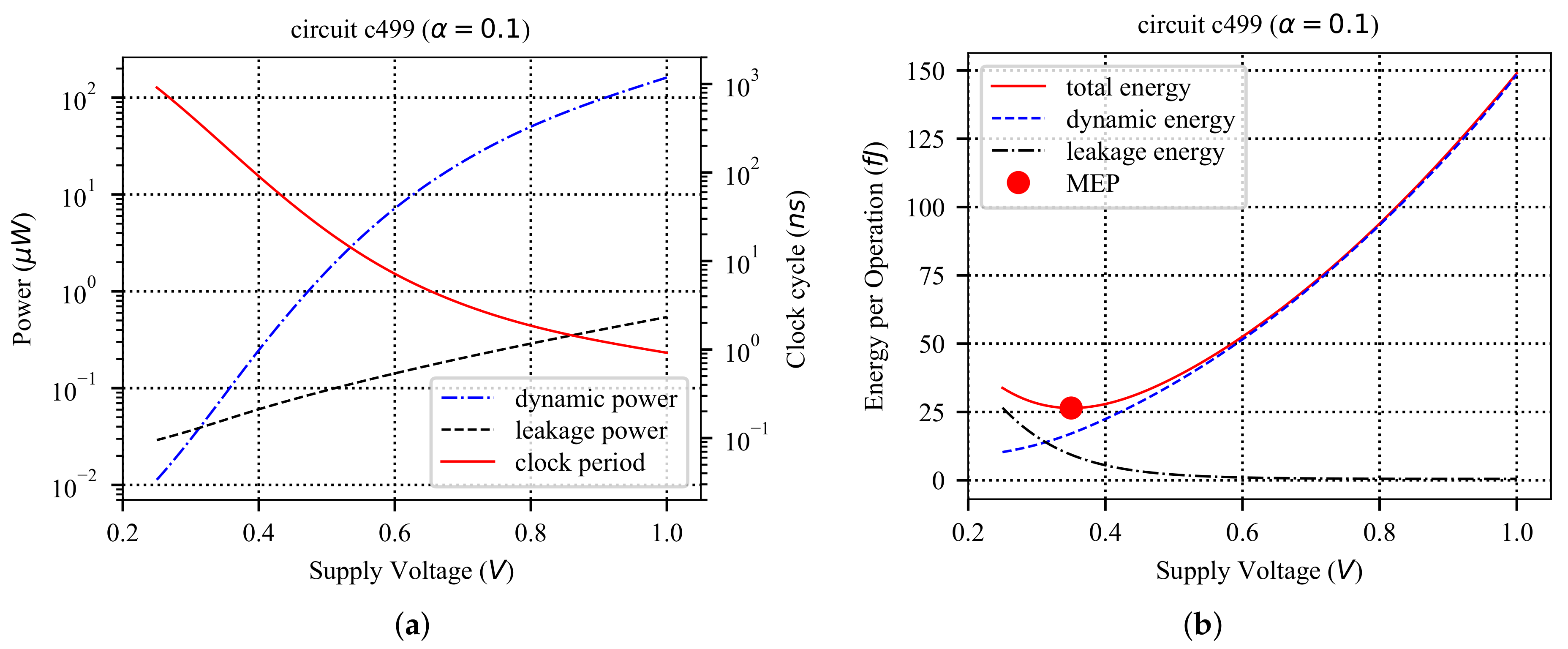
 .
.
.
.
 . (a) Executing instruction OPA on original functional unit and the associated leakage dissipation by unexercised components. (b) Executing instruction OPA on the partitioned functional unit and power-gating of smaller units.
. (a) Executing instruction OPA on original functional unit and the associated leakage dissipation by unexercised components. (b) Executing instruction OPA on the partitioned functional unit and power-gating of smaller units.
. (a) Executing instruction OPA on original functional unit and the associated leakage dissipation by unexercised components. (b) Executing instruction OPA on the partitioned functional unit and power-gating of smaller units.


| Baseline | Proposed Multi-Cycling Approach | ||||||
|---|---|---|---|---|---|---|---|
| Clock Period | Data Type | Energy () | Time (s) | Energy () | Time (s) | Energy Improvement | Performance Improvement |
| 73 ns | short (2-bytes) | 27.9 | 502 | 22.2 | 502 | 20.3% | 0.1% |
| char (1-byte) | 22.5 | 404 | 17.6 | 396 | 21.5% | 2% | |
| Overall improvement (baseline-short → multi-cycling-char) | 36.9% | 21.1% | |||||
| 49 ns | short (2-bytes) | 27.9 | 502 | 20.5 | 459 | 26.5% | 8.6% |
| char (1-byte) | 22.5 | 404 | 15.9 | 356 | 29.0% | 12% | |
| Overall improvement (baseline-short → multi-cycling-char) | 42.9% | 29.2% | |||||
| Area Overhead (%) | Performance Improvement (%) | Energy Saving for Power-Gating Threshold () in % | ||||||
|---|---|---|---|---|---|---|---|---|
| 10 Cycles | 20 Cycles | 50 Cycles | 100 Cycles | 500 Cycles | ||||
| 3-ALU | 17 | 11 | 0.80 (super-) | 22.8 | 19.7 | 19.5 | 19.4 | 17.7 |
| 7.0 | 0.35 (near- *) | 24.6 | 21.4 | 21.2 | 21.1 | 19.2 | ||
| 5.5 | 0.25 (sub-) | 27.7 | 24.4 | 24.1 | 24.0 | 21.8 | ||
| 4-ALU | 19 | 11 | 0.80 (super-) | 43.1 | 38.6 | 32.1 | 27.6 | 15.1 |
| 7.0 | 0.35 (near-) | 43.4 | 38.9 | 33.0 | 28.9 | 17.3 | ||
| 5.5 | 0.25 (sub-) | 44.1 | 39.6 | 34.5 | 31.1 | 20.6 | ||
Publisher’s Note: MDPI stays neutral with regard to jurisdictional claims in published maps and institutional affiliations. |
© 2020 by the authors. Licensee MDPI, Basel, Switzerland. This article is an open access article distributed under the terms and conditions of the Creative Commons Attribution (CC BY) license (http://creativecommons.org/licenses/by/4.0/).
Share and Cite
Tahoori, M.; Golanbari, M.S. Cross-Layer Reliability, Energy Efficiency, and Performance Optimization of Near-Threshold Data Paths. J. Low Power Electron. Appl. 2020, 10, 42. https://0-doi-org.brum.beds.ac.uk/10.3390/jlpea10040042
Tahoori M, Golanbari MS. Cross-Layer Reliability, Energy Efficiency, and Performance Optimization of Near-Threshold Data Paths. Journal of Low Power Electronics and Applications. 2020; 10(4):42. https://0-doi-org.brum.beds.ac.uk/10.3390/jlpea10040042
Chicago/Turabian StyleTahoori, Mehdi, and Mohammad Saber Golanbari. 2020. "Cross-Layer Reliability, Energy Efficiency, and Performance Optimization of Near-Threshold Data Paths" Journal of Low Power Electronics and Applications 10, no. 4: 42. https://0-doi-org.brum.beds.ac.uk/10.3390/jlpea10040042