Article

Energy Efficiency in Slew-Rate Enhanced Single-Stage OTAs for Switched-Capacitor Applications

Dipartimento di Ingegneria dell’Informazione, University of Pisa, Via Girolamo Caruso, 16, 56122 Pisa, Italy
*
Authors to whom correspondence should be addressed.
These authors contributed equally to this work.
J. Low Power Electron. Appl. 2021, 11(1), 1; https://0-doi-org.brum.beds.ac.uk/10.3390/jlpea11010001
Submission received: 15 November 2020 / Revised: 8 December 2020 / Accepted: 21 December 2020 / Published: 24 December 2020
(This article belongs to the Special Issue Low-Power CMOS Analog and Digital Circuits and Filters)

Abstract

:
Slew-rate enhancement (SRE) techniques assist the charge transfer process in OTA-based switched-capacitor circuits. Parallel-type slew-rate enhancement circuits, i.e., circuits that provide a feed-forward path external to the main OTA, are attractive solutions, since they introduce a further degree of freedom in the speed/power consumption design space without affecting other specifications regarding the main OTA. This technique lends itself to be employed jointly with advanced OTA topologies in order to compose a highly energy efficient OTA/SRE system. However, insights in design choices such as power optimization are still missing for such systems. Here we discuss system level choices with the help of a simple model. Using precise electrical simulations, we demonstrate energy savings greater than 30% for different OTA/SRE systems implemented in a standard 180-nm CMOS technology.

1. Introduction

The settling behaviour of Switched-Capacitor (SC) stages, as the one depicted in Figure 1a, has been conveniently described by a simplified model [1,2,3,4,5,6,7,8]. This model breaks down the charge-transfer operation in a SC stage, whether a SC amplifier or a SC integrator, into two phases, corresponding to the idealized operating regions of the OTA: slew rate and linear regions. Hence, the total settling time, t S , is then given by two contributions t 1 (slew-rate time) and t 2 (linear time) as:
t S = t 1 + t 2 , and t 1 = Δ V i ( 0 + ) V d m a x C S I o m a x ; t 2 = τ · ln V d m a x V i n ϵ ,
where: Δ V i ( 0 + ) is the initial step seen at the OTA’s input due to the charge redistribution at t = 0 , proportional to Δ V S through the attenuation factor C S / [ C S + C P + C F C L / ( C F + C L ) ] ; I o m a x is the OTA’s maximum output current; C S = ( C S + C P ) ( 1 + C L / C F ) + C L ; V d m a x discriminates the OTA’s operation region (slew rate for | V i | V d m a x , linear for | V i | < V d m a x ), V i n ϵ = ϵ R Δ V S C S / ( C S + C P + C F ) ; where ϵ R is the relative error on the output voltage step and finally τ = C S / G m is the time constant in the linear transient of a single-pole OTA, being G m the OTA’s transconductance.
As shown in Figure 1a, we are interested in the case of large voltage steps which trigger the OTA to operate initially in its slewing region. This leads us to point out that both t 1 and t 2 depends on Δ V S respectively through Δ V i ( 0 + ) and V i n ϵ . On the other hand, Equation (1) explicitly shows how V d m a x , which is a design parameter, influences the settling time, both in the t 1 and the t 2 terms also. For a Class-A OTA, like the common folded-cascode (FC) OTA, V d m a x can be identified with the range of operation of the input differential pair. When sized to operate in weak inversion to achieve the maximum current efficiency [9], V d m a x = 2 n U T , being n the sub-threshold slope and U T the thermal voltage ( 25.7 mV at 25 ° C).
Figure 1b shows the relative impact of t 1 on the overall settling as a function of the input voltage step assuming the conventional FC OTA modeled from (1). For this OTA, a simple linear relationship between its G m (weak inversion operation of input devices) and I o m a x exists, which can be easily shown to be: τ I o m a x = 2 n U T C S . This fact allows us to eliminate all the transistor-level design parameters from t 1 / t S . The design space, for this particular case, can be represented as a family of curves parameterized for a given capacitive network ( C S , C F , C L , C P ) and the relative error ϵ R . In Figure 1b two design cases, named “high-resolution” and “low-resolution”, are shown. They correspond to the respective parameters sets in the inset table. These are typical values, mainly derived from k T / C -noise specifications, that can be found in high-resolution (≥16 bits) and low-resolution (12 bits or less) systems. Marginally, specific transistor-level design choices (sizing of input devices) affect C P , but as long as C P is sufficiently smaller than C S , the model accuracy is not compromised. The main OTA, depending on the specific application case, follows design optimization taking into account many other aspects, such as offset, low-frequency noise. Using a parallel-type SRE, the speed/power-consumption trade-off can be targeted without affecting other design parameters.
In order to achieve the best signal-to-noise ratio, Δ V S is set equal to the maximum magnitude of the input step voltage that we assume to be the supply voltage V d d . Moving from one technological node to another, distinct supply voltage domains are given. In Figure 1b, the V d d regions for 1.2 V, 1.8 V, 3.3 V can be associated to the 65-nm, 180-nm and 350-nm CMOS processes, respectively. As expected, the lower V d d the lower is the impact of t 1 on t S . However, even for the 1.2-V/low-resolution case t 1 is approximately the 75% of t S , justifying the need for power-efficient circuit techniques to reduce t 1 . For example, by reducing t 1 to one third of its original value, t S would be halved. Intuitively this t S reduction can be translated to a design situation where t S is maintained, but the total power consumption is scaled down. We recently proposed a capacitive-boosted slew-rate enhancer (SRE) technique fit to this purpose [10] based on Nagaraj’s SRE [11,12]. Nevertheless, a systematic study of this technique to provide clear system-level design insight is still missing.
Here we want to address this issue by analyzing the performances of the SRE technique when combined with more advanced OTA configurations, such as the recycling folded cascode (RFC) [13]. The remainder of this paper is organized as follows: Section 2 develops the settling-time model for power-aware system-level choices; Section 3 introduces energy metrics to evaluate the performances of different OTA/SRE systems by the means of accurate electrical simulations; Section 4 concludes this work by stating the major findings.

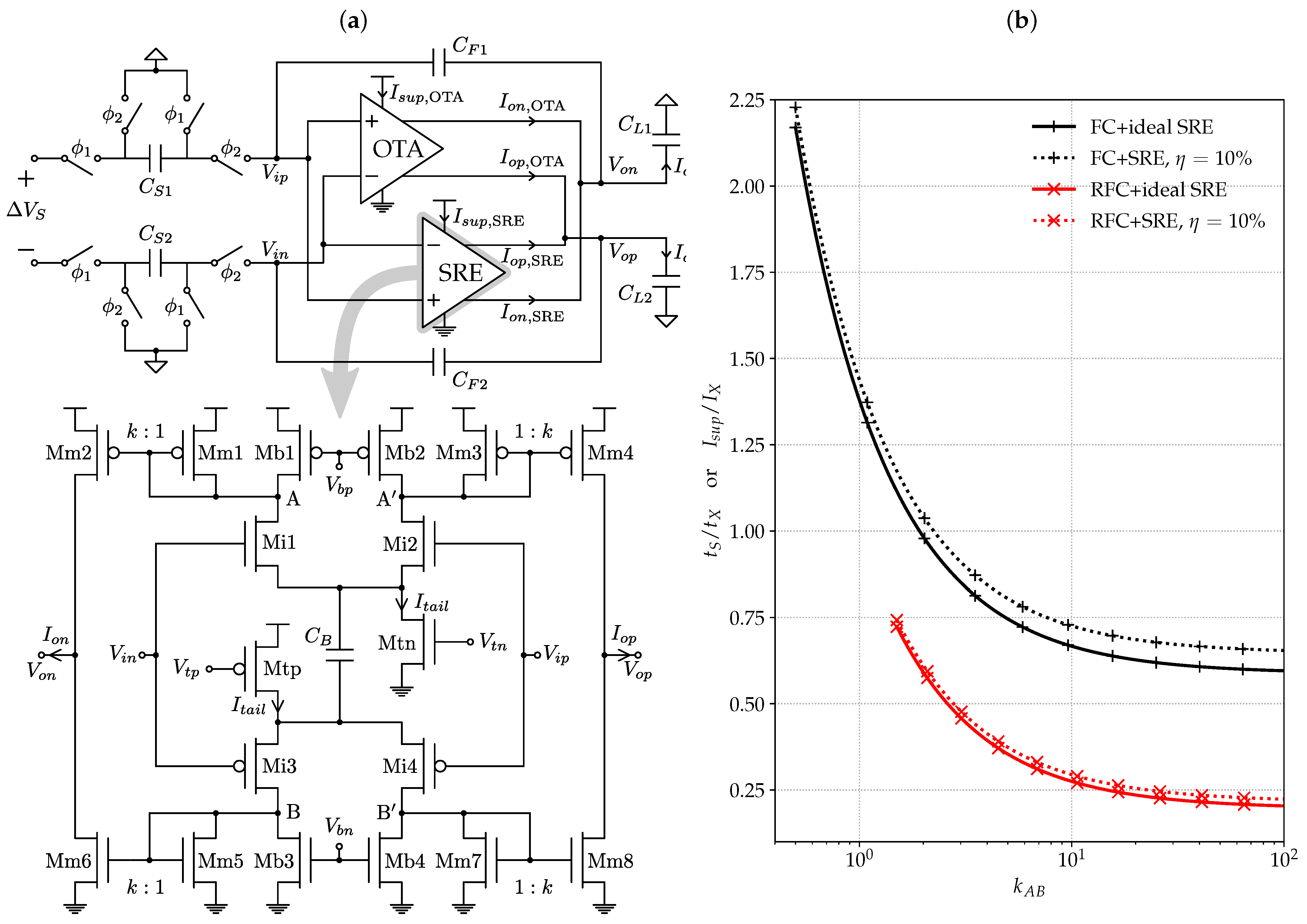
2. Extened Settling-Time Model

2.1. System-Level Settling Model

We recently introduced an extension of model in (1) concerning system-level parameters [10]. This model is useful to describe the settling behaviour of the SC stage in Figure 1a whether it employs a single-stage OTA, or a OTA/SRE system:
t S t X = 1 k A B c 1 V d m a x Δ V S + 1 k G V d m a x Δ V S ln c 2 ϵ R V d m a x Δ V S .
The two addends in the right hand side of (2) correspond to t 1 and t 2 of (1) respectively, normalized by the time t X . Indeed, Equation (2) descends from Equation (1), once the following identities are defined:
t X = C S Δ V S I s u p ; c 1 = C S C S + C P 1 C L C S ; c 2 = 1 + C F + C P C S ; k A B = I o m a x I s u p ; k G = G m V d m a x I s u p .
As evident from (3), the model of (2) emphasizes the role of the quiescent current I s u p drawn by the circuit from the supply rail. The parameters in (2) have the following meaning:
  • t X acts as a normalizing unit for t S taking into account system-level specifications regarding the capacitive load C S , the input step amplitude Δ V S , and the current consumption I s u p .
  • c 1 and c 2 : both parameters mainly depend on the capacitive feedback network C S , C F , C L and the OTA’s input parasitic capacitance C P .
  • k A B expresses the efficiency by which the OTA uses the given I s u p to produce its output current when operating in slew-rate region.
  • k G expresses the efficiency by which the OTA uses the given I s u p to produce large transconductance when operating in linear region.
By applying the following transformation:
t S t X = t S I s u p C S Δ V S = I s u p I X , where I X = C S Δ V S t S .
We observe that the same expression in (2) can be used to estimate the static current consumption I s u p needed for a given t S , while maintaining the rest of the constraints. The normalizing current I X , similarly to t X , takes into account only system-level specifications.

2.2. Model Extension to OTA/SRE Systems

Figure 2a shows a typical Fully-Differential SC integrator configuration. It is possible to demonstrate its equivalence in terms of settling time with the single-ended circuit in Figure 1a, considering voltages and currents of the single-ended model representing the total differential-mode components of the fully-differential circuit in Figure 2a. It can be easily shown that the only transformation that has to be applied regards the input capacitance of the OTA in the equivalent circuit, C P in Figure 1a, that should be set to twice the input capacitance of the fully-differential OTA. Considering Figure 2a, the other capacitances of the circuit are simply replicated in the single-ended equivalent, i.e., C S = C S 1 = C S 2 , C F = C F 1 = C F 2 , C L = C L 1 = C L 2 .
The SRE of [10] provides a parallel signal path in order to assist the OTA during the charge transfer process; its transistor-level schematic is also shown in Figure 2a. The SRE delivers non-zero output currents only during the slew rate time t 1 , while mirrors Mm1-Mm8 are ideally turned off afterwards. This behaviour is achieved thanks to the current comparison occurring at nodes A-A’ and B-B’ under the action of Mb1-Mb2 and Mb3-Mb4 transistors which are set to subtract a fixed amount of current I t h , determining the turn-on/off threshold of the SRE. For large input differential voltage ( > V d m a x ), the SRE provides an amount of current equal in magnitude to I o m a x , SRE .
The introduction of the SRE adds a static current consumption indicated with I s u p , SRE = 2 I t a i l . Its maximum output current capability is then measured by:
k A B , SRE = I o m a x , SRE I s u p , SRE = k 1 I t h I t a i l ,
since the SRE is statically biased by 2 I t a i l (bias chain not included) and, by considering a robust sizing with I t h = 3 I t a i l / 4 , it is capable to deliver k I t a i l / 4 at the output under maximum unbalanced condition. Actually, SREs with large values of k together with low I t a i l , which would represent an optimum design choice for the SRE, show a degradation of their effectiveness. The capacitive-boosting proposed in [10] and implemented by the capacitor C B shown in Figure 2a solves this issue and has been adopted in this work.
From the design point of view, the SRE input commutation threshold is designed to coincide with voltage V d m a x , that defines the boundary between the input regions where the OTA behaves in a linear and non-linear (saturated) fashion. The threshold-conditioned behaviour of the SRE is similar to that of comparator-based SC circuits introduced in [14]. Ideally, comparator-based SC circuits has a null linear settling time ( t 2 = 0 corresponding to V d m a x = 0 ) making t S = t 1 . This condition is extremely beneficial from the power-efficiency point of view since the current drawn from the supply rail is almost entirely used to charge directly the load. In practice, the absence of virtual ground prevents comparator-based SC solutions to be used in medium/high resolution applications. In our case the SRE always operates in parallel with an OTA in order to ensure precise virtual ground settling and thus circumventing the linearity limitations typical of comparator-based SC circuits.
From the system point of view, the overall static current consumption is now composed by the OTA’s contribution I s u p , OTA and the SRE’s contribution I s u p , SRE ; this can be accounted for by defining the η parameter such that:
η = I s u p , SRE I s u p , OTA and I s u p = I s u p , OTA + I s u p , SRE = ( 1 + η ) I s u p , OTA .
As already stated, the settling time model in (2) is valid also for OTA/SRE system, with due attention to the expressions of k A B and k G . The former, being related to the maximum output current, is given by the combined action of the OTA and SRE, while the latter is strictly related to the G m of the OTA alone which is now biased by a portion of the total supply current, namely I s u p / ( 1 + η ) :
k A B = I o m a x , OTA + I o m a x , SRE I s u p = k A B , OTA + η k A B , SRE 1 + η ; k G = k G , OTA 1 + η .
Figure 2b shows the settling time t S and I s u p while increasing the k A B of the OTA/SRE system for both the FC and RFC OTA topologies. Solid traces show the possible reduction in t S / t X or I s u p / I X when using an ideal SRE (no static power) to increase the k A B . A more realistic prediction is shown by the dotted traces, which account for a η = 10 % budget. In any case, substantial benefit of the SRE action is predicted by the model. Detailed discussion on RFC vs. FC parameters ( k A B , k G and V d m a x ) is presented in the following section.

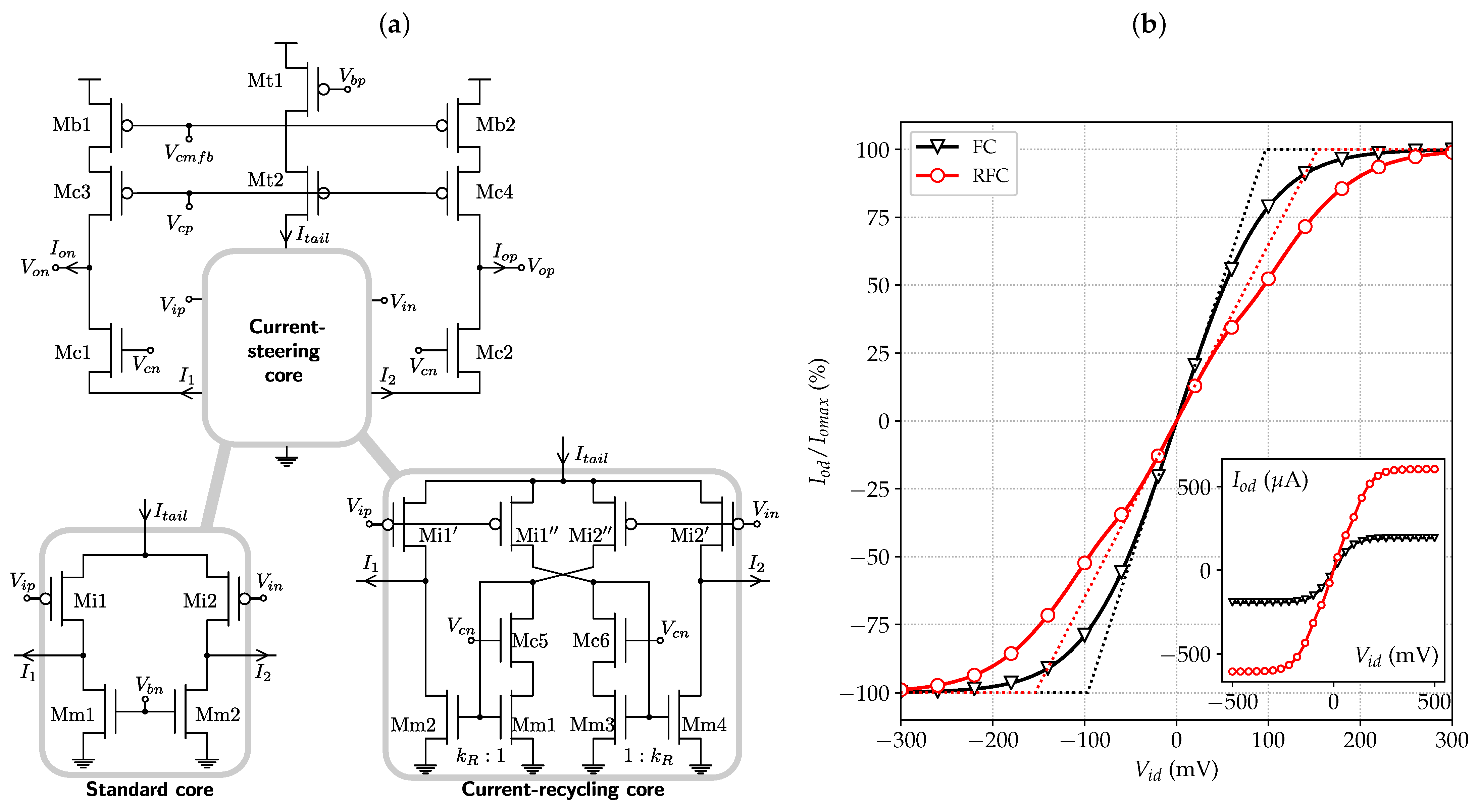
2.3. Model Extension to Advanced OTA Topologies

The validity of the model in (2) for advanced single-stage OTA architectures, such as RFC [13], Super-Class AB [15], VMA [16] has not been yet demonstrated. The model in (1) and hence (2) hinges on a piece-wise linear approximation of OTA’s characteristic of the output differential current as function of input differential voltage, i.e., I o d ( V i d ) . A hard threshold, V d m a x , is set between large-signal and small-signal regions. Within the V d m a x range, i.e., | V i d | < V d m a x , the model considers the linear small-signal circuit approximation. Outside the V m a x range, i.e., | V i d | V d m a x , the model considers perfect saturation of currents to the I o m a x value. This highly simplified model is intrinsically prone to inaccuracy [2,3] and cannot be used to fine tune any final design, for which accurate electrical simulations are still needed [17]. Nevertheless it provides a uniform and simple analytic tool useful to compare different OTAs and OTA/SRE architectures, as will be shown in the following discussion.
Here we will discuss the RFC topology [13] as exemplary case study for mapping advanced single-stage OTAs to the model in (2). Although the methodology is of general applicability, exhaustive mapping of other advanced OTA families, as those stemming from [15,16], are beyond the scope of this paper.
Figure 3a shows a conceptual schematic of folded cascode architectures formed by a current-steering core and an output section. The current-steering core is in charge to provide the differential voltage to differential current conversion and to properly bias the rest of the circuit. The output section provides low-impendance inputs for the differential current (through Mc1-Mc2) and high-impedance output of the whole OTA.
The FC and the RFC OTAs are obtained when the current-steering core is implemented as the standard and the current-recycling core, respectively, as shown in Figure 3a. The RFC core is obtained by equally splitting the input devices to create an auxiliary current path. Thanks to the action of mirrors Mm1-Mm2 and Mm3-Mm4, both the G m and the I o m a x are enhanced with respect to the FC. Theoretically, in the case of k R = 3 , G m is multiplied by 2 and I o m a x is multiplied by 3. This enhancement comes without any static power penalty [13].
Considering now the piecewise approximation, since no discontinuities are present, the relationship I o m a x = G m V d m a x is set for both the FC and the RFC OTA. Since in the RFC architecture I o m a x and G m scale differently, the V d m a x parameter needs to scale accordingly, i.e., V d m a x , RFC = 3 2 V d m a x , FC . From the circuit point of view, the wider V d m a x is due to the mirrors Mm1-Mm2 and Mm3-Mm4 which provide both biasing and signal propagation, differently from what happens in the standard core where the NMOS section only provides biasing currents.
Electrical simulations confirm the theoretical behaviour as shown in Figure 3b where the I o d ( V i d ) characteristics are shown for both the FC and RFC. The inset shows the actual FC and RFC characteristics, resulting in I o m a x , RFC / I o m a x , FC = 3.13 and G m , RFC / G m , FC = 1.97 . The main plot is normalized to the maximum output current for each topology. The relative piecewise asymptotes are also reported for comparison. The extracted V d m a x parameters are found to be 97.0 mV and 154.0 mV for the FC and the RFC, respectively, which are in good agreement with the expected scaling factor. The normalized I o d values for V i d = V d m a x are 77.6% (FC) and 77.2% (RFC) indicating that the impact of non-linearities on the model prediction accuracy is very close, and that, in both cases, the analytical techniques proposed in [2,3] would be equally effective to mitigate inaccuracy.

3. Energy Efficiency of OTA/SRE Systems

The transient of the SC circuit in Figure 1a implies a quantity of charge delivered to the effective load capacitance C L seen at OTA’s output:
C L = C L + C F ( C S + C P ) C S + C P + C F .
The magnitude of the total charge delivered from the OTA to C L depends on the total voltage swing at the output node, Δ V o L :
Δ V o L = | Δ V o ( 0 + ) | + ( 1 ϵ R ) | Δ V o ( ) | | Δ V o ( 0 + ) | + | Δ V o ( ) | ,
where the Δ V o ( 0 + ) and the Δ V o ( ) are easily calculated from the initial charge redistribution and the asymptotic value for an ideally infinite open-loop gain OTA:
Δ V o ( 0 + ) = C S ( C F + C L ) ( C S + C P ) ( C F + C L ) + C F C L Δ V S ; Δ V o ( ) = C S C F Δ V S .
Under the action of the fully-differential OTA (or OTA/SRE system), the power supply delivers the charge Q L , given by:
Q L = 1 2 C L Δ V o L .
Note that in differential-circuits the Δ V o L variation is equally distributed between the output nodes ( V o p and V o n in Figure 2a) around the common mode of the OTA. For the sake of clarity, let us assume that V o p and V o n undergo a variation of + 1 2 Δ V o L and 1 2 Δ V o L , respectively. Discharge at V o n node occurs due to charge flow to the ground rail, so Q L is only given by the charge variation at V o p node. This fact accounts for the 1/2 factor in (11). Finally, the energy E L needed for the charge transfer is calculated considering (8)–(11):
E L = Q L · V d d = 1 2 C L Δ V o L · V d d .
It is important to observe that E L is proportional to Δ V S (see (10)) through a rather complex function of the capacitor network. While C S , C F and C L values derive directly from system-level specifications, C P is the result of a specific OTA design. First-hand estimation of E L , prior any OTA design, can be done neglecting C P in (8), (10) and asserting the condition C P C S in the aftermath.
In a system where the stochastic or pseudo-stochastic characteristics Δ V S are known, like in a SC Δ Σ modulator [18], E L can be used to estimate the energy needed for signal processing purposes, regardless of the overheads due to the employment of actual circuits. A simple electrical testbench can be employed to numerically calculate the actual energy, E s u p , drawn from the supply rail by the OTA or OTA/SRE for a single transition step ( Δ V S ). The normalized E s u p / E L quantity may be employed as a useful indicator to optimize the OTA or OTA/SRE system tailored to its final application. In such testbench different OTA(/SRE) topologies can be tested for efficiency comparison aiding the search for power optimization among different topological solutions.
As exemplary design cases, specifications in Table 1 are assumed. We will discuss the application of the SRE technique in both a FC and RFC topologies in comparison with the FC and RFC alone aiming to fulfill the same settling speed and precision ( t S = 15 ns, ϵ R = 100 ppm). Regular NMOS and PMOS devices from the UMC 180-nm CMOS process under 1.8-V supply condition are assumed. The comparison methodology starts by designing a FC OTA (FC1) compliant with the specifications in Table 1. The next step is to consider the FC/SRE system, for η = 10 % , C B = 500 fF and k = 30 which are a valid set of parameters for nearly optimum behaviour of the SRE [10]. For this configuration the FC biasing currents and its input devices are scaled to maintain the same current density in the input devices and to attain to the same settling time (FC2). A further step is to consider the RFC topology (RFC1) which embeds power-efficient class-AB behaviour. Finally, the RFC/SRE system is considered, with the correspondent current and input devices scaling (RFC2). Since the SRE is completely turned off in the last part of the settling, the noise, offset and gain properties of the original OTA are left unchanged.
Actual transistor parameters and biasing currents are also reported in Table 1. The I t a i l current predicted by the model Equations (2), (4) and (7), together with the mirror ratios k = 30 for the SRE, k R = 3 for the RFC and η = 10 % are: 375 μ A for FC1, 195 μ A for FC2, 152 μ A for RFC1 and 96 μ A for RFC2. The FC-OTA parameters are k A B , FC = k G , FC = 0.5 , while the RFC-OTA parameters are k A B , FC = k G , FC = 1.5 , calculated applying the definitions in (3). The input devices are biased in weak inversion operation in all cases, so that V d m a x , FC = 98.8 mV and V d m a x , RFC = 148.2 mV. Note that the SRE commutation threshold has been kept around V d m a x , FC in both cases for the sake of simplicity; further optimization can be achieved in the SRE/RFC2 design. k A B , SRE has been estimated from the electrical simulations, due to the lack of a proper description of the capacitive-boosting technique effects in the modeling approach. As discussed in [10], the relation (5) is valid only neglecting the turn-on and turn-off transients of the SRE circuit. The actual k A B , SRE , calculated through electrical simulations, is found to be 41.5.
The I t a i l estimation is quite accurate for FC1 and FC2, while the evident underestimation for RFC1 and RFC2 can be ascribed to the simplistic modeling. More specifically, it derives from the phase-margin degradation of the RFC topology due to the non-dominant pole determined by the current mirrors Mm1-Mm2 and Mm3-Mm4 (see Figure 3a). In such condition the single-pole OTA approximation used in Equation (1) is not accurate, reinforcing the need for more refined models to abstract circuit behaviour including the presence of non-dominant singularities in the OTA frequency response [8].
Table 2 lists the results from electrical simulation using Spectre/Cadence. As expected, the use of the SRE greatly enhances the E s u p / E L figure of merit in both cases, i.e., FC1 vs. FC2 + SRE and RFC1 vs. RFC2 + SRE, which in the second case showed to be even more beneficial than in the first case. Interestingly, the use of the SRE coupled to the standard FC showed to surpass the efficiency performances of the RFC alone, proving to be a quite effective and versatile technique. In absolute terms, the energy reduction enabled by the SRE is 34% for both the FC and the RFC topology. The t 1 / t S has been also estimated using the model with the k G corrected values. In the first case, a reduction of almost 1/5 is obtained, while in the second case the slew-rate time is approximately divided by three. As already mentioned, offset and noise performances are not affected by the action of the SRE, with respect to the OTAs considered individually. For this reason we do not report comparative figures in Table 2.

4. Conclusions

This work discuss energy efficiency optimization by using parallel-type SRE circuits to assist single-stage OTAs in the charge transfer process. Detailed electrical simulations demonstrated that power savings greater of 30% are achieved both when using standard Class-A OTAs and more advanced OTA topologies like the recycling folded cascode topology. The optimization process is aided by a simple model useful to fairly compare different OTA topologies. Model accuracy limitations, when used to predict absolute power figures, are also discussed.

Author Contributions

All authors participated to the conceptualization and methodology of this work. Data curation, A.C., M.C., M.D.; writing–original draft preparation, A.C., M.C., M.D.; writing–review and editing: M.P., P.B. All authors have read and agreed to the published version of the manuscript.

Funding

This project has received funding from the European Union’s Horizon 2020 research and innovation programme under the Marie Skłodowska-Curie grant agreement No. 893544.

Data Availability Statement

Data is contained within the article.

Conflicts of Interest

The authors declare no conflict of interest. The funders had no role in the design of the study; in the collection, analyses, or interpretation of data; in the writing of the manuscript, or in the decision to publish the results.

References

  1. Sansen, W.M.C.; Qiuting, H.; Halonen, K.A.I. Transient analysis of charge-transfer in SC filters-gain error and distortion. IEEE J. Solid-State Circuits 1987, 22, 268–276. [Google Scholar] [CrossRef]
  2. Robertini, A.; Goette, J.; Guggenbuhl, W. Nonlinear distortions in SC-integrators due to nonideal switches and amplifiers. IEEE Int. Sympos. Circuits Syst. 1989, 3, 1692–1695. [Google Scholar] [CrossRef]
  3. Robertini, A.; Guggenbuhl, W. Errors in SC circuits derived from linearly modeled amplifiers and switches. IEEE Trans. Circuits Syst. I Fund. Theory Appl. 1992, 39, 93–101. [Google Scholar] [CrossRef]
  4. Wang, F.; Harjani, R. Power analysis and optimal design of op amps for oversampled converters. IEEE Trans. Circuits Syst. II Analog Digit. Signal Process. 1999, 46, 359–369. [Google Scholar] [CrossRef]
  5. del Rio, R.; Medeiro, F.; Perez-Verdu, B.; Rodriguez-Vazquez, A. Reliable analysis of settling errors in SC integrators-application to the design of high-speed ΣΔ modulators. In Proceedings of the 2000 IEEE International Symposium on Circuits and Systems (ISCAS), Geneva, Switzerland, 28–31 May 2000; Volume 4, pp. 417–420. [Google Scholar] [CrossRef] [Green Version]
  6. Suarez, G.; Jimenez, M.; Fernandez, F.O. Behavioral Modeling Methods for Switched-Capacitor ΣΔ Modulators. IEEE Trans. Circuits Syst. I Regul. Pap. 2007, 54, 1236–1244. [Google Scholar] [CrossRef]
  7. Karnstedt, C. Optimizing Power of Switched Capacitor Integrators in Sigma-Delta Modulators. IEEE Circuits Syst. Mag. 2010, 10, 64–71. [Google Scholar] [CrossRef]
  8. Boni, A.; Giuffredi, L.; Pietrini, G.; Magnanini, A.; Tonelli, M. Design-oriented model for power-driven design optimization of SC-ΔΣ modulators. Int. J. Circ. Theor. Appl. 2018, 46, 707–728. [Google Scholar] [CrossRef]
  9. Hollis, T.M.; Comer, D.J.; Comer, D.T. Optimization of MOS amplifier performance through channel length and inversion level selection. In Proceedings of the IEEE Transactions on Circuits and Systems II: Express Briefs, Taormina, Italy, 2–3 September 2005; Volume 52, pp. 545–549. [Google Scholar] [CrossRef]
  10. Catania, A.; Cicalini, M.; Dei, M.; Piotto, M.; Bruschi, P. Performance Analysis and Design Optimization of Parallel-Type Slew-Rate Enhancers for Switched-Capacitor Applications. Electronics 2020, 9, 1949. [Google Scholar] [CrossRef]
  11. Nagaraj, K. Slew rate enhancement method for folded-cascode amplifiers. Electr. Lett. 1989, 25, 19. [Google Scholar] [CrossRef]
  12. Nagaraj, K. CMOS amplifiers incorporating a novel slew rate enhancement technique. In Proceedings of the IEEE Custom Integrated Circuits Conference, Boston, MA, USA, 13–16 May 1990; pp. 11.6/1–11.6/5. [Google Scholar] [CrossRef]
  13. Assaad, R.S.; Silva-Martinez, J. The Recycling Folded Cascode: A General Enhancement of the Folded Cascode Amplifier. IEEE J. Solid-State Circuits 2009, 44, 2535–2542. [Google Scholar] [CrossRef]
  14. Fiorenza, J.K.; Sepke, T.; Holloway, P.; Sodini, C.G.; Lee, H. Comparator-Based Switched-Capacitor Circuits for Scaled CMOS Technologies. IEEE J. Solid-State Circuits 2006, 41, 2658–2668. [Google Scholar] [CrossRef]
  15. Lopez-Martin, A.J.; Baswa, S.; Ramirez-Angulo, J.; Carvajal, R.G. Low-Voltage Super class AB CMOS OTA cells with very high slew rate and power efficiency. IEEE J. Solid-State Circuits 2005, 40, 1068–1077. [Google Scholar] [CrossRef]
  16. Sutula, S.; Dei, M.; Terés, L.; Serra-Graells, F. Variable-Mirror Amplifier: A New Family of Process-Independent Class-AB Single-Stage OTAs for Low-Power SC Circuits. IEEE Trans. Circuits Syst. I Regular Pap. 2016, 63, 1101–1110. [Google Scholar] [CrossRef] [Green Version]
  17. Cisneros-Fernández, J.; Terés, L.; Dei, M.; Serra-Graells, F. Design methodology for power-efficient SC delta-sigma modulators based on switched-VMAs. In Proceedings of the 2017 32nd Conference on Design of Circuits and Integrated Systems (DCIS), Barcelona, Spain, 22–24 November 2017; pp. 1–6. [Google Scholar] [CrossRef]
  18. Cisneros-Fernández, J.; Serra-Graells, F.; Terés, L.; Dei, M. A Compact Switched-Capacitor Multi-Bit Quantizer for Low-Power High-Resolution Delta-Sigma ADCs. In Proceedings of the 2018 IEEE International Symposium on Circuits and Systems (ISCAS), Florence, Italy, 27–30 May 2018; pp. 1–5. [Google Scholar] [CrossRef]
Figure 1. SC circuit and its relevant waveforms under the charge transfer process for a stimulus of Δ V S (a); Slew-rate time over total settling time as function input voltage step Δ V S considering a folded-cascode OTA with input pair working in weak inversion ( V d m a x = 2 n U T ) (b). Colored bands correspond to voltage supply ( V d d ) regions considering n ranging from 1.5 and 2.0, room temperature conditions. The numerical values of the circuit parameters for high-resolution and low-resolution cases are indicated in table.
Jlpea 11 00001 g001
Figure 2. SC integrator with OTA/SRE combination: (a) topology of the parallel-type SRE employing capacitive boosting. (b) Plot of t S / t X as a function of k A B for two different OTA topologies combined with an ideal (no power consumption) and real ( η = 10 % ) SRE. Note that different k A B values correspond to different design choices for the SRE. The relative settling time t S / t X can be converted to a relative supply current consumption I s u p / I X through (4).
Jlpea 11 00001 g002
Figure 3. Fully-differential folded cascode architectures: (a) standard and current-recycling steering cores; (b) input/output characteristics.
Jlpea 11 00001 g003
Table 1. Specifications and OTAs design parameters used in the testbech.
Specifications
t S 15ns
Δ V S 1.8V
C S 1.5pF
C F 6.0pF
C L 1.0pF
ϵ R 100ppm
SRE, I t a i l = 20 μ A,
C B = 500 fF.
L (nm)W ( μ m)
Mi1-21801.50
Mi3-41804.50
Mm1, Mm31801.62
Mm2, Mm418048.60
Mm5, Mm71800.54
Mm6, Mm818016.20
Mtn10002.88
Mtp10000.96
Mb1-210002.16
Mb3-410000.72
L (nm)W ( μ m)
Mi1-2180480
Mm1-240032
Mc1-218072
Mc3-4180288
Mb1-240073
Mt1400146
Mt2180576
L (nm)W ( μ m)
Mi1-2180240
Mm1-240032
Mc1-218072
Mc3-4180288
Mb1-240073
Mt1400146
Mt2180576
L (nm)W ( μ m)
Mi1 -1″-2 -2″180156
Mm1-340016
Mm2-440048
Mc5-618036
Mc1-218072
Mc3-418028
Mb1-240073
Mt1400146
Mt218072
L (nm)W ( μ m)
Mi1 -1″-2 -2″18078
Mm1-340016
Mm2-440048
Mc5-618036
Mc1-218072
Mc3-418028
Mb1-240073
Mt1400146
Mt218072
Table 2. Electrical simulation results and impact of slew-rate time on the overall settling time ( t 1 / t S ) estimated by means of the proposed model.
FC1FC2 + SRERFC1RFC2 + SRE
t S  (ns)14.9814.6914.6414.61
E s u p  (pJ)21.9314.4915.5210.3
C P  (fF)701358528270
E L  (pJ)3.133.143.133.15
E s u p / E L 7.004.614.953.27
( t 1 / t S ) (%)49.810.538.811.9
Publisher’s Note: MDPI stays neutral with regard to jurisdictional claims in published maps and institutional affiliations.

