A Morphable Physically Unclonable Function and True Random Number Generator Using a Commercial Magnetic Memory

 , and
, and
Abstract
:1. Introduction
- We characterize the MRAM bit-to-bit write latency under voltage and temperature variations.
- We characterize the MRAM response under multiple write disturbs which can be useful for TRNG.
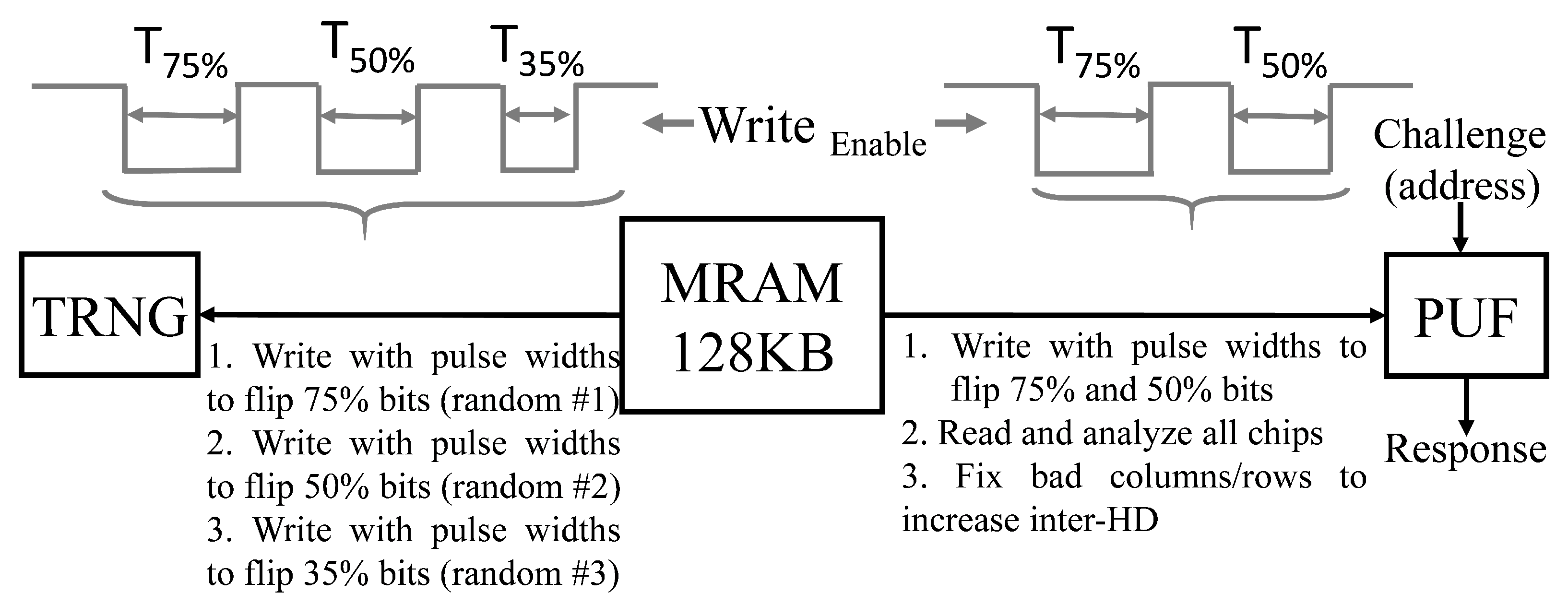
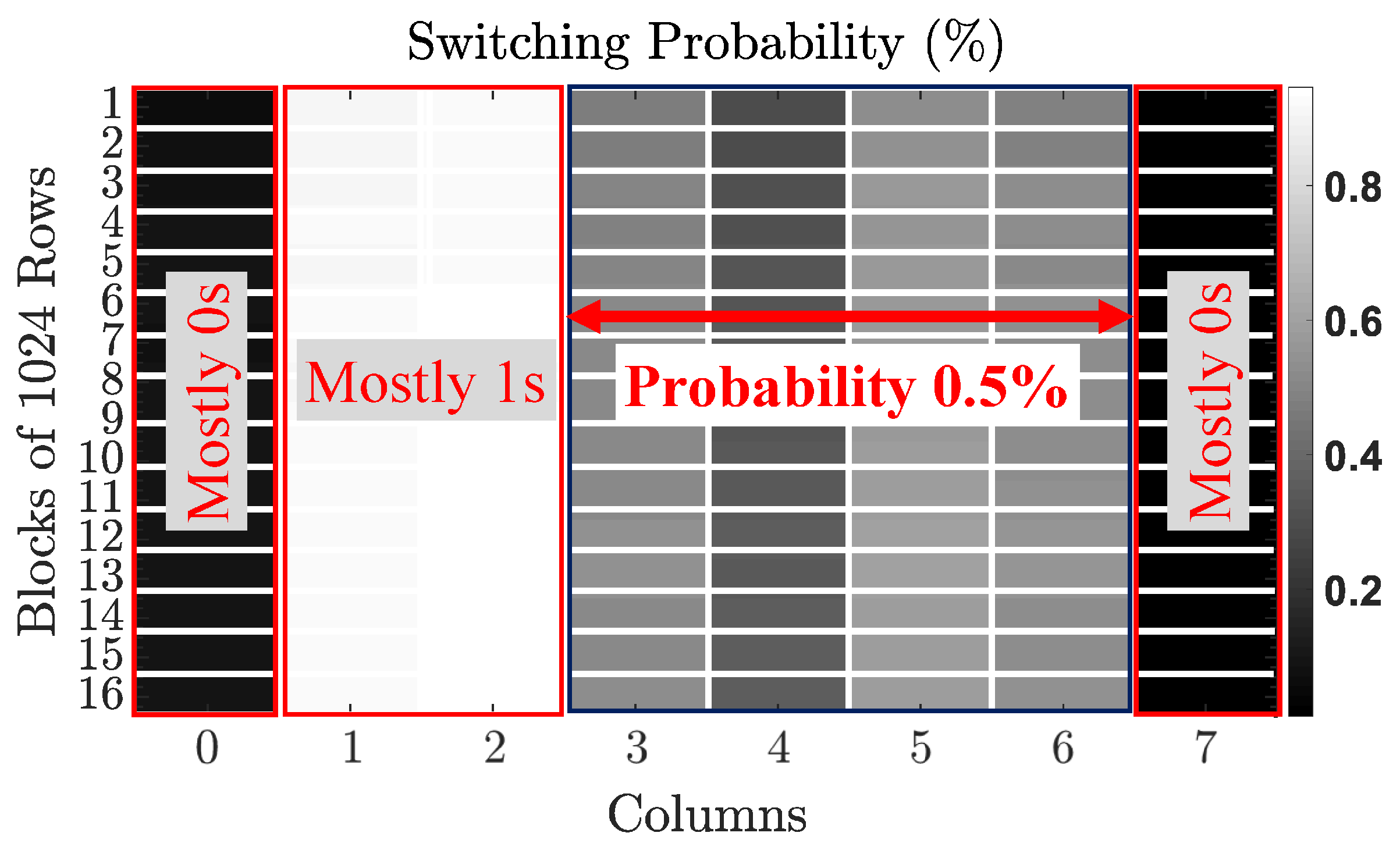
- We propose a write PUF (wPUF) by biasing the MRAM with a write latency with 50% switching probability. The proposed PUF exhibits excellent stability and uniqueness.
- We show that 75% of the bits could be unresponsive to a challenge and propose techniques to convert them into useful bits avoiding expensive row and columns masking.
- We propose a TRNG by exploiting random MRAM responses under multiple write disturbs.
- We benchmark the proposed PUF and TRNG with existing designs.
2. Background on MRAM and Its Variation
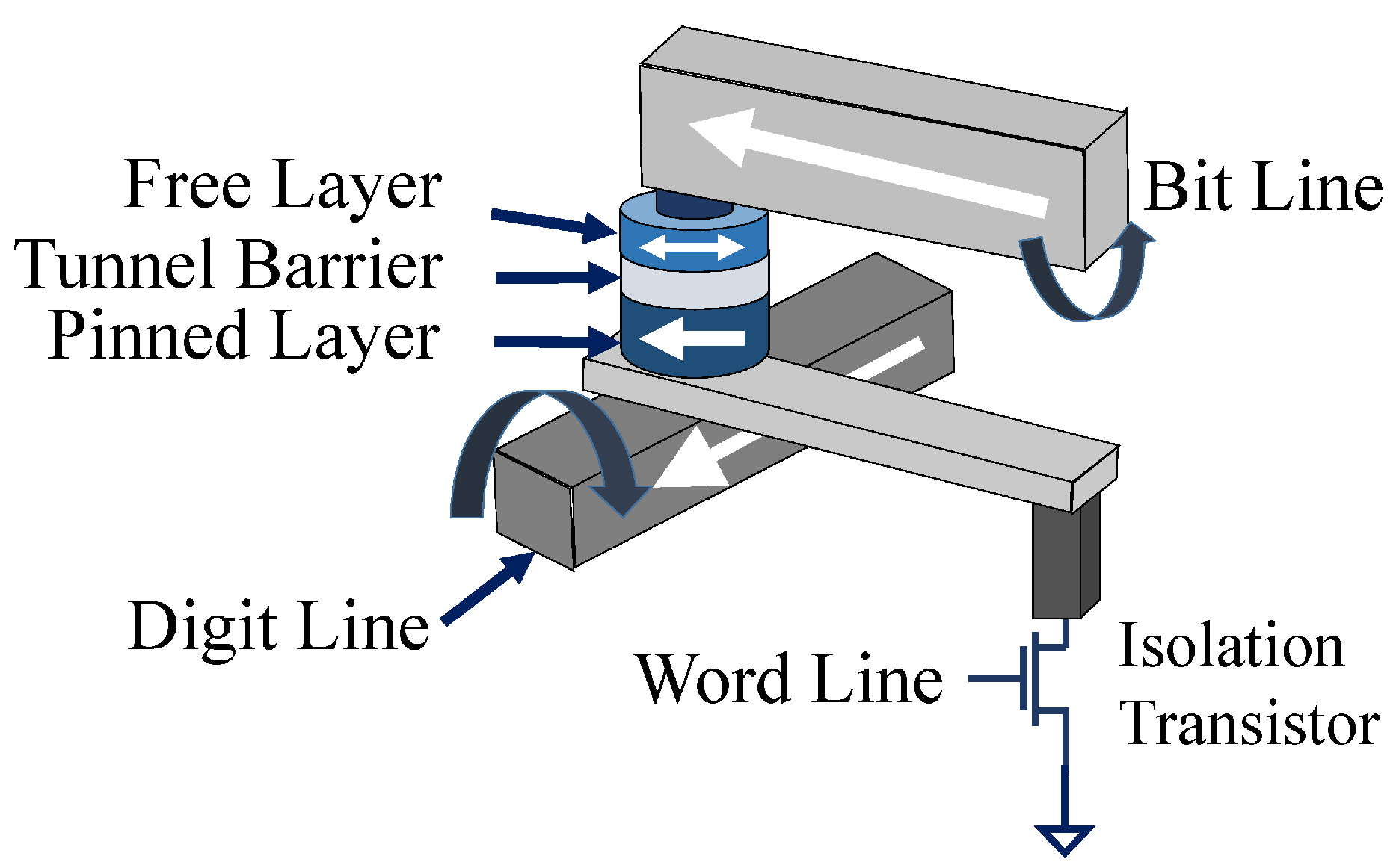
2.1. Basics of MRAM
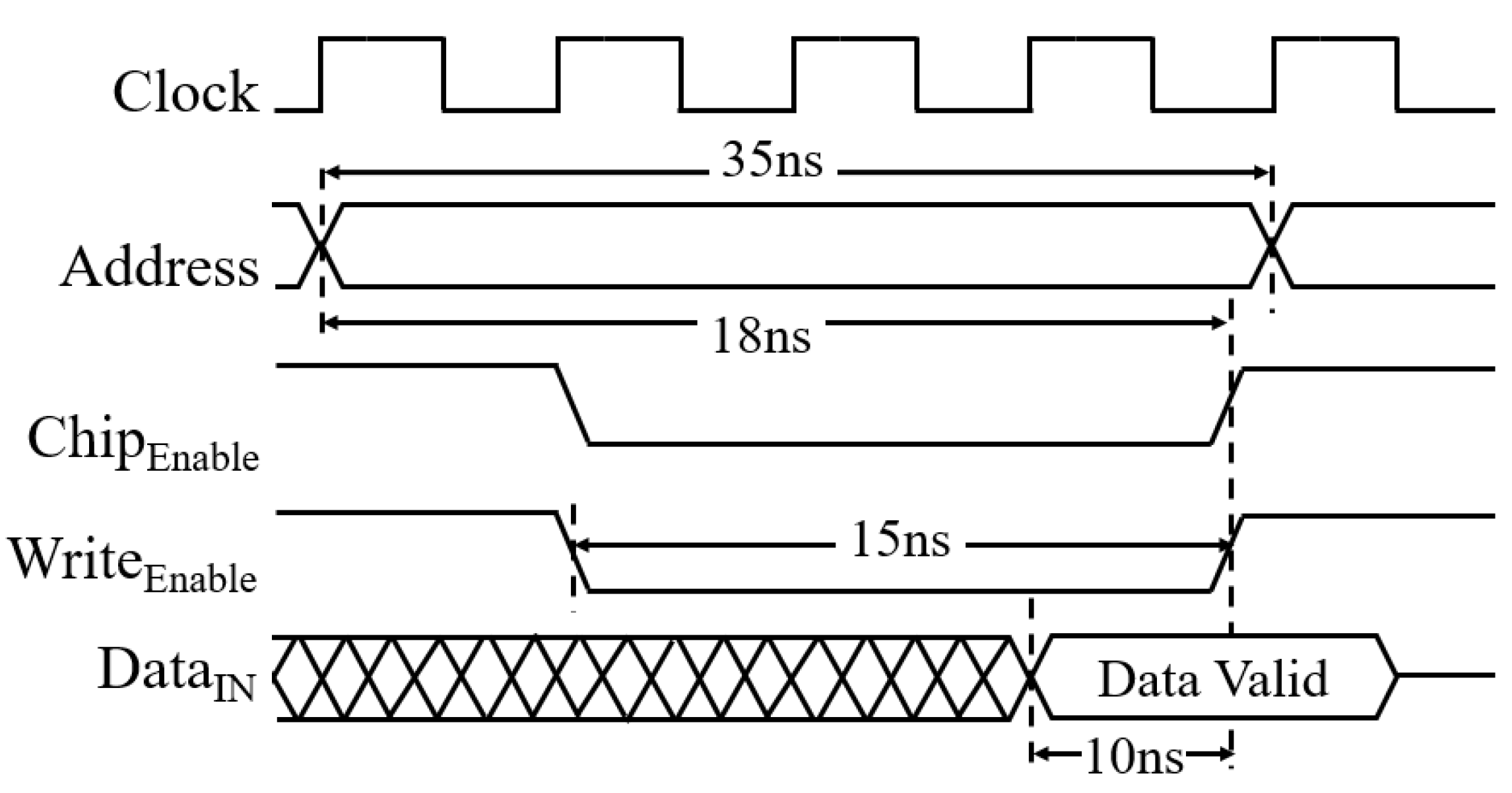
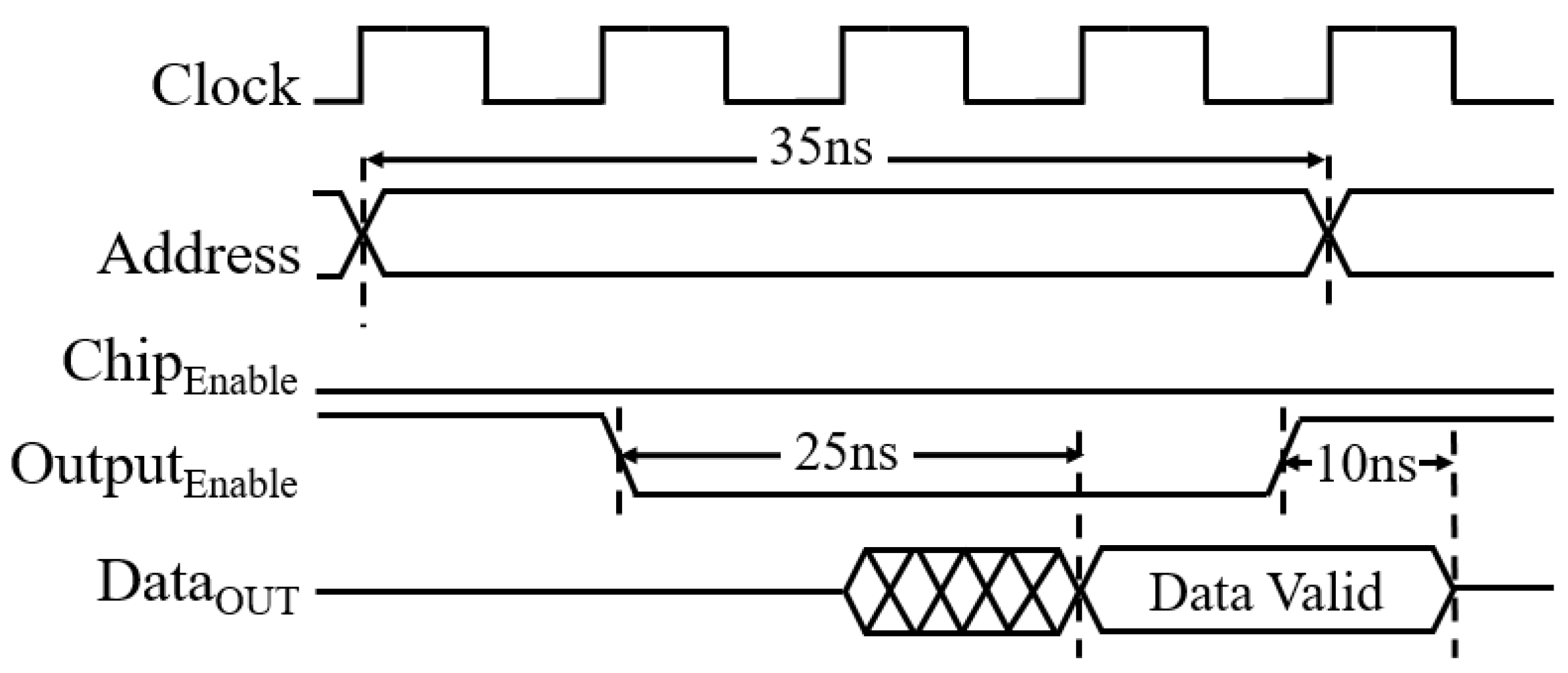
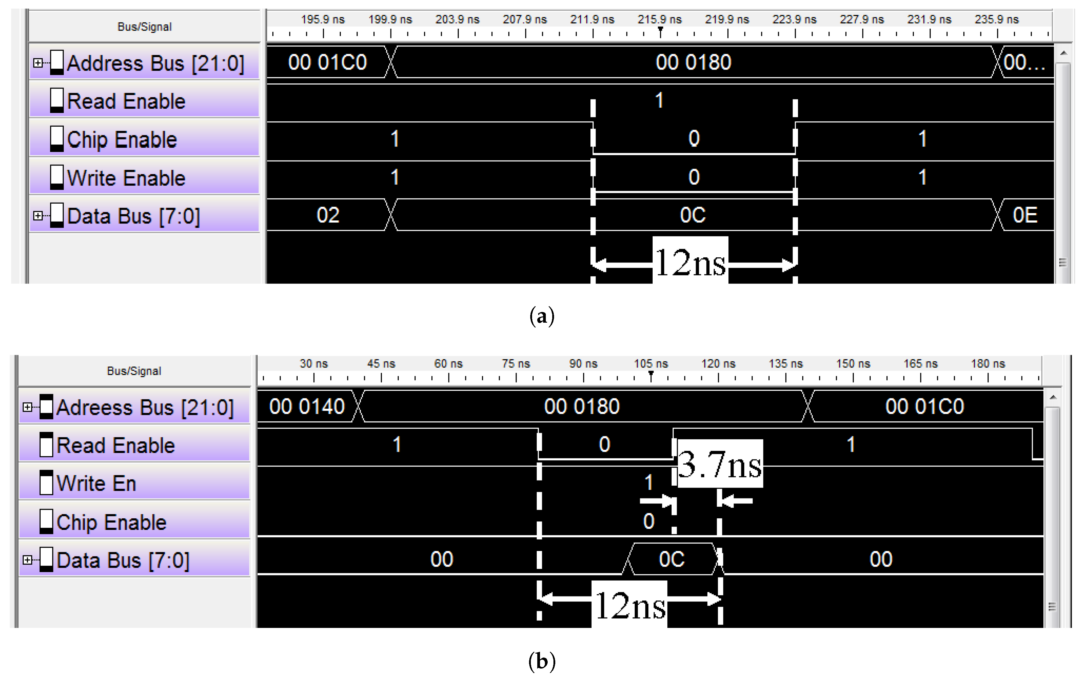
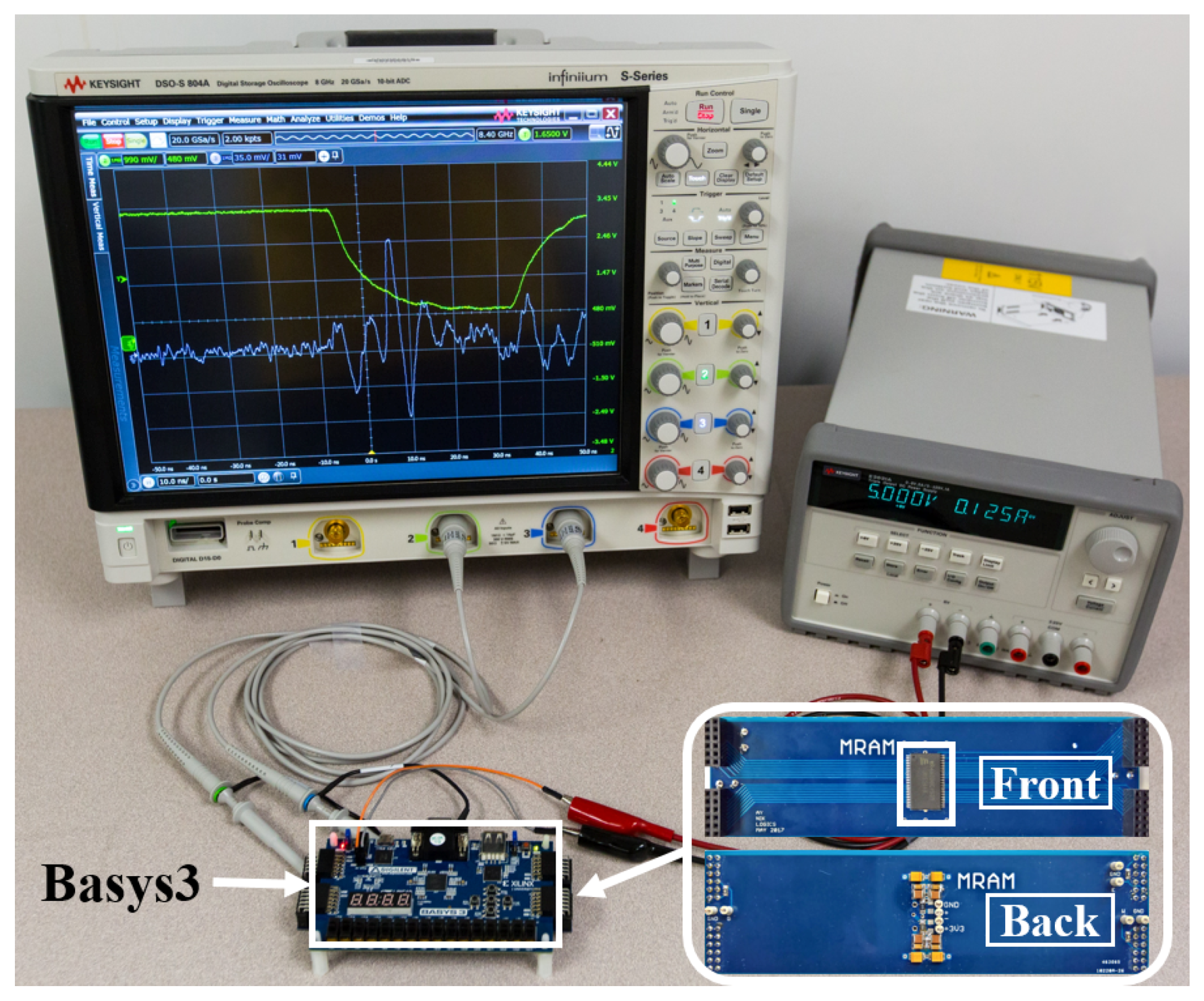
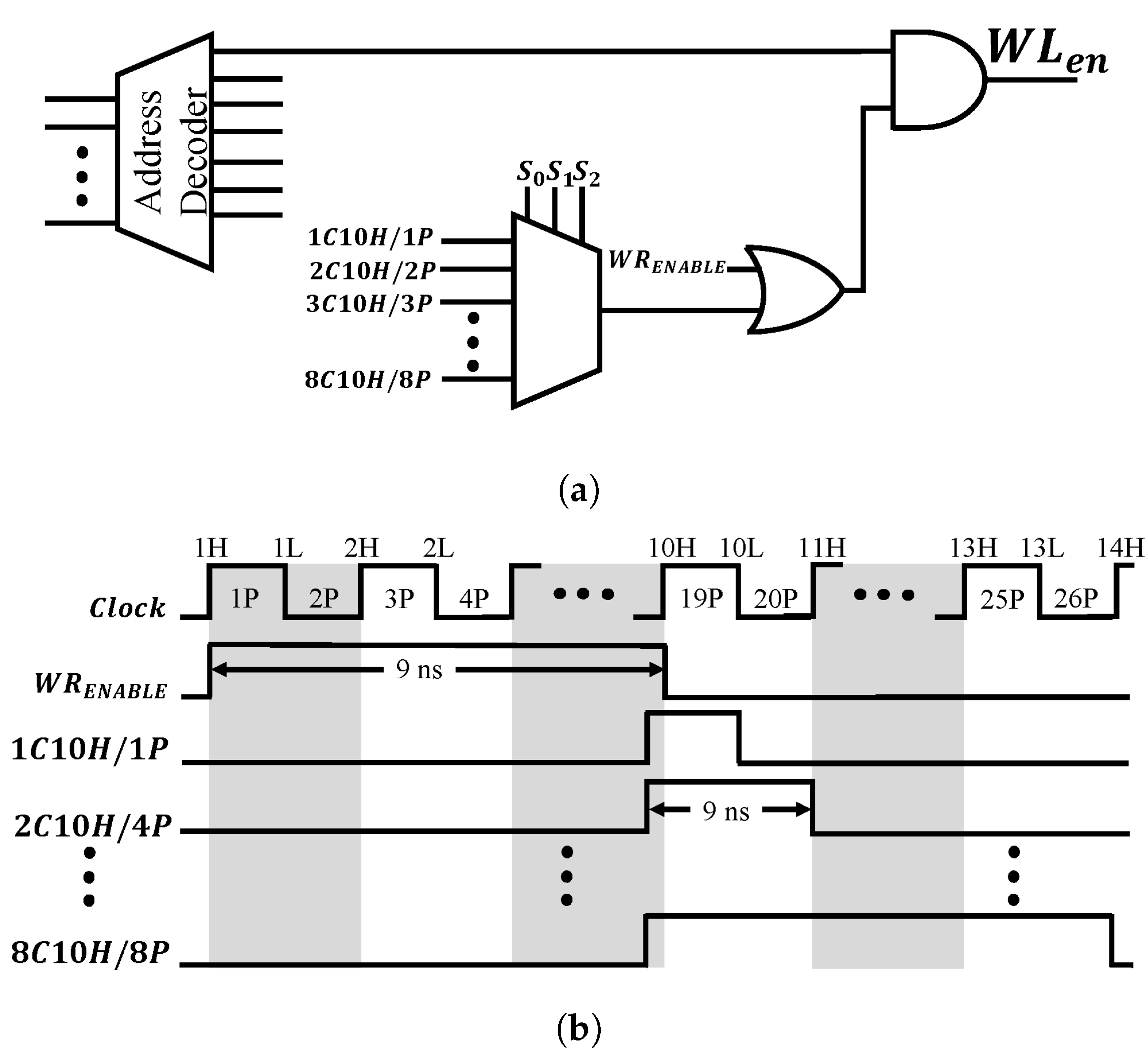
2.2. Experimental Setup
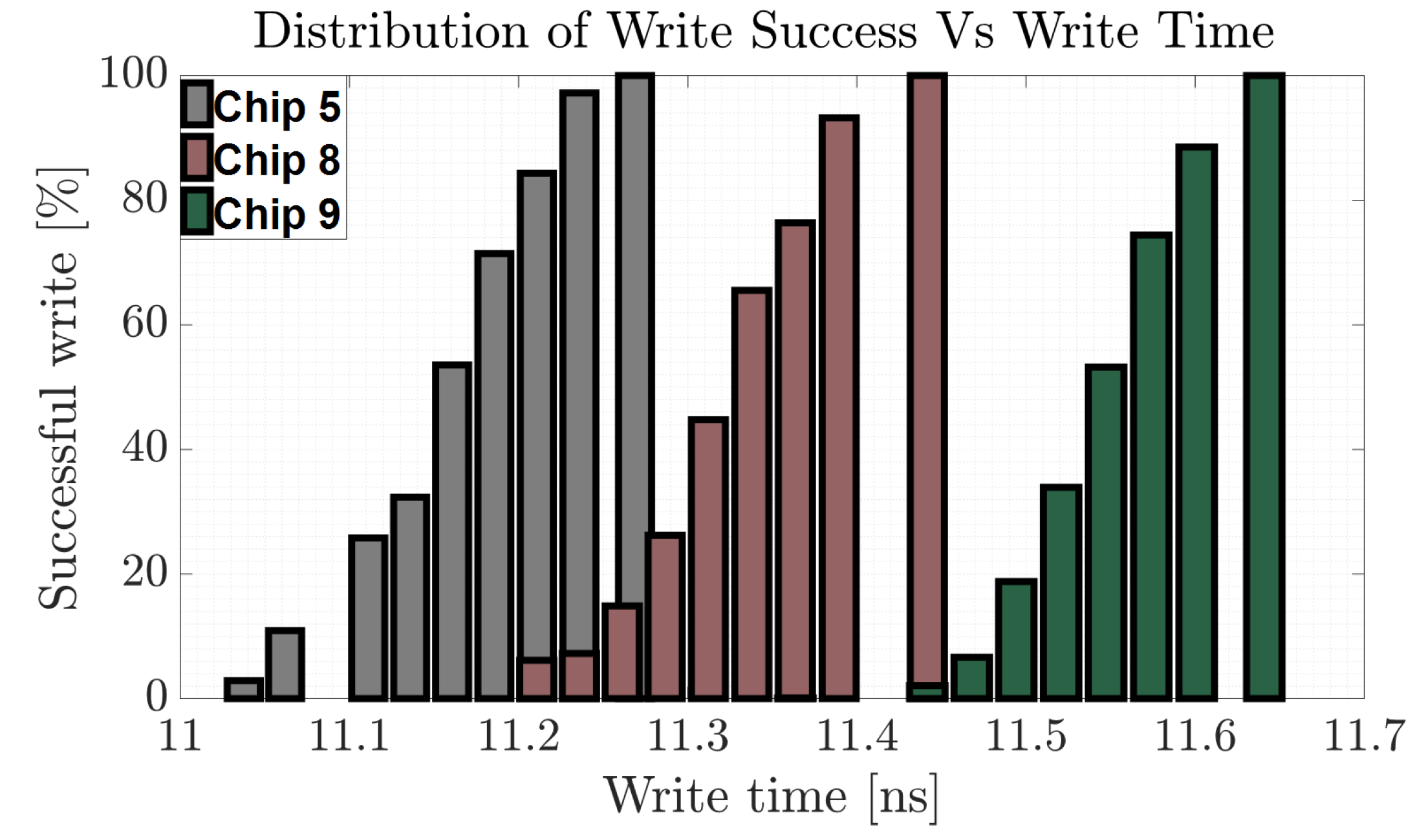
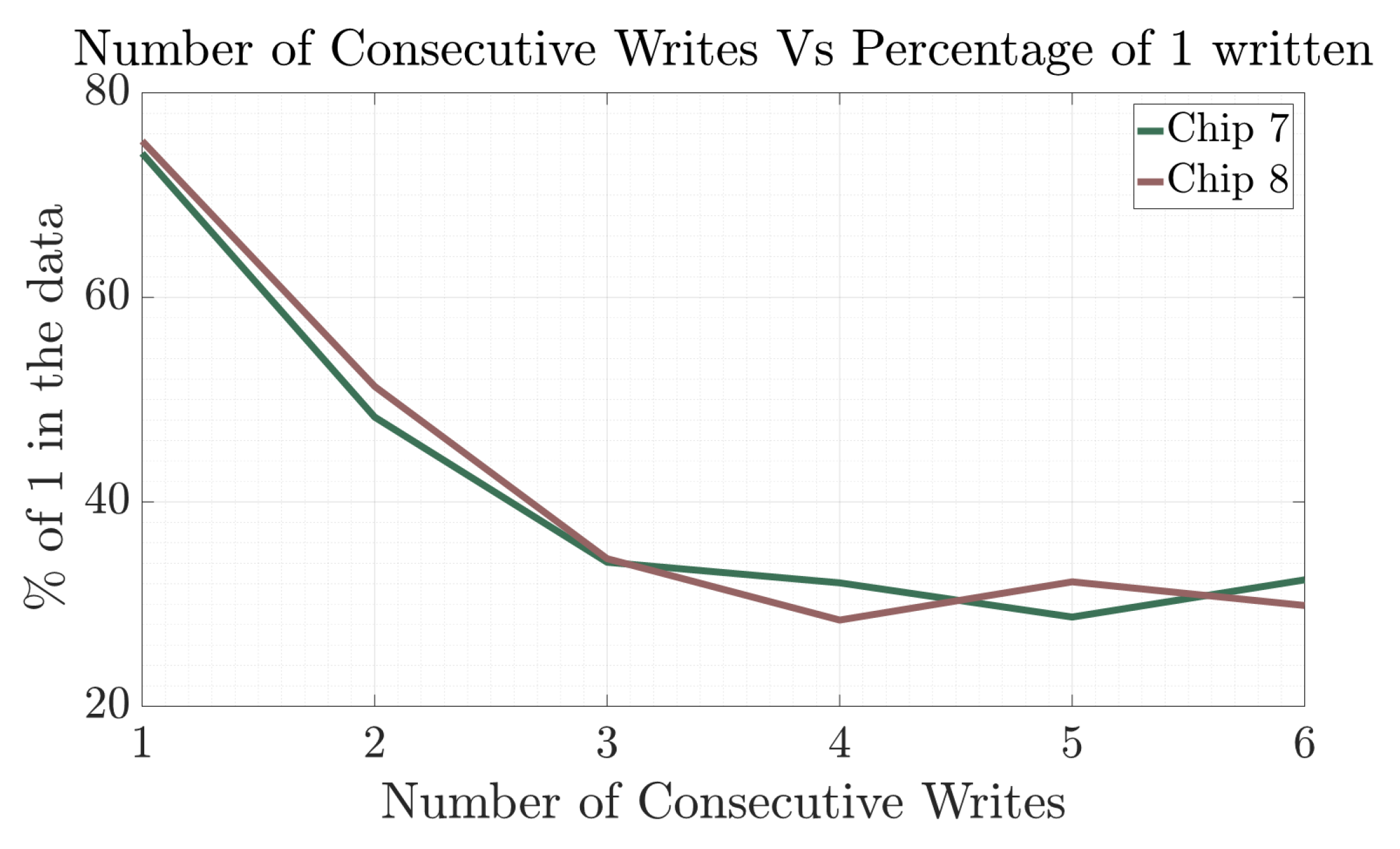
2.3. Switching Variation of MRAM
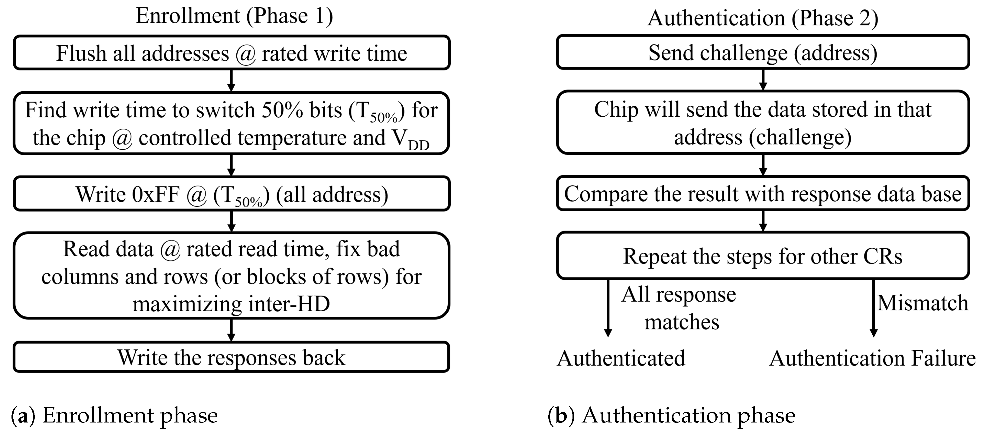
3. PUF
3.1. Proposed wPUF
3.2. Performance Analysis
3.2.1. Uniqueness (Inter-Die HD)
3.2.2. Reliability (Intra-Die HD)
3.2.3. Uniformity
3.3. Improving Inter-HD
3.3.1. Improving Column Performance
3.3.2. Improving Row Performance
4. TRNG
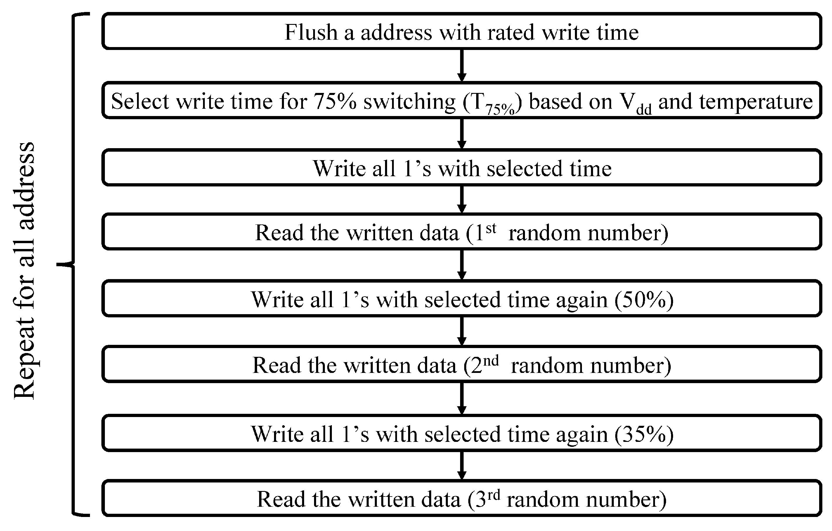
4.1. Proposed TRNG
4.2. Performance Analysis
5. Discussions
6. Conclusions
Author Contributions
Funding
Conflicts of Interest
References
- Khan, M.N.I.; Bhasin, S.; Yuan, A.; Chattopadhyay, A.; Ghosh, S. Side-Channel Attack on STTRAM Based Cache for Cryptographic Application. In Proceedings of the 2017 IEEE International Conference on Computer Design (ICCD), Boston, MA, USA, 5–8 November 2017; pp. 33–40. [Google Scholar]
- Lin, C.W.; Ghosh, S. Novel self-calibrating recycling sensor using Schmitt-Trigger and voltage boosting for fine-grained detection. In Proceedings of the Sixteenth International Symposium on Quality Electronic Design, Santa Clara, CA, USA, 2–4 March 2015; pp. 465–469. [Google Scholar]
- Herder, C.; Yu, M.; Koushanfar, F.; Devadas, S. Physical Unclonable Functions and Applications: A Tutorial. Proc. IEEE 2014, 102, 1126–1141. [Google Scholar] [CrossRef]
- Suh, G.E.; Devadas, S. Physical Unclonable Functions for Device Authentication and Secret Key Generation. In Proceedings of the 2007 44th ACM/IEEE Design Automation Conference, San Diego, CA, USA, 4–8 June 2007; pp. 9–14. [Google Scholar]
- Tsoi, K.H.; Leung, K.H.; Leong, P.H.W. Compact FPGA-based true and pseudo random number generators. In Proceedings of the 11th Annual IEEE Symposium on Field-Programmable Custom Computing Machines, FCCM 2003, Napa, CA, USA, 9–11 April 2003; pp. 51–61. [Google Scholar]
- Magnetic Tamper Detection Using Low-PowerHall Effect Sensors. Available online: http://www.ti.com/lit/ug/tidub69/tidub69.pdf (accessed on 12 January 2021).
- Miura, N.; Fujimoto, D.; Tanaka, D.; Hayashi, Y.-I.; Homma, N.; Aoki, T.; Nagata, M. A local EM-analysis attack resistant cryptographic engine with fully-digital oscillator-based tamper-access sensor. In Proceedings of the 2014 Symposium on VLSI Circuits Digest of Technical Papers, Honolulu, HI, USA, 10–13 June 2014; pp. 1–2. [Google Scholar]
- Ghosh, S.; Basak, A.; Bhunia, S. How Secure Are Printed Circuit Boards Against Trojan Attacks? IEEE Design Test 2015, 32, 7–16. [Google Scholar] [CrossRef]
- Khan, M.N.I.; Nagarajan, K.; Ghosh, S. Hardware Trojans in Emerging Non-Volatile Memories. In Proceedings of the 2019 Design, Automation & Test in Europe Conference & Exhibition (DATE), Florence, Italy, 25–29 March 2019; pp. 396–401. [Google Scholar]
- Khan, M.N.I.; De, A.; Ghosh, S. Cache-Out: Leaking Cache Memory Using Hardware Trojan. IEEE Trans. Very Large Scale Integr. (VLSI) Syst. 2020, 28, 1461–1470. [Google Scholar] [CrossRef]
- Mazady, A.; Rahman, M.T.; Forte, D.; Anwar, M. Memristor PUF—A Security Primitive: Theory and Experiment. IEEE J. Emerg. Sel. Top. Circuits Syst. 2015, 5, 222–229. [Google Scholar] [CrossRef]
- Iyengar, A.; Ghosh, S.; Ramclam, K.; Jang, J.-W.; Lin, C.-W. Spintronic PUFs for Security, Trust, and Authentication. J. Emerg. Technol. Comput. Syst. 2016, 13, 1–5. [Google Scholar] [CrossRef]
- Ghosh, S.; Govindaraj, R. Spintronics for associative computation and hardware security. In Proceedings of the 2015 IEEE 58th International Midwest Symposium on Circuits and Systems (MWSCAS), Fort Collins, CO, USA, 2–5 August 2015; pp. 1–4. [Google Scholar]
- Chen, A. Utilizing the Variability of Resistive Random Access Memory to Implement Reconfigurable Physical Unclonable Functions. IEEE Electron Device Lett. 2015, 36, 138–140. [Google Scholar] [CrossRef]
- Zhang, L.; Fong, X.; Chang, C.; Kong, Z.H.; Roy, K. Highly reliable memory-based Physical Unclonable Function using Spin-Transfer Torque MRAM. In Proceedings of the 2014 IEEE International Symposium on Circuits and Systems (ISCAS), Melbourne, VIC, Australia, 1–5 June 2014; pp. 2169–2172. [Google Scholar]
- Chen, A.; Hu, X.S.; Jin, Y.; Niemier, M.; Yin, X. Using emerging technologies for hardware security beyond PUFs. In Proceedings of the 2016 Design, Automation & Test in Europe Conference & Exhibition (DATE), Dresden, Germany, 14–18 March 2016; pp. 1544–1549. [Google Scholar]
- Das, J.; Scott, K.; Rajaram, S.; Burgett, D.; Bhanja, S. MRAM PUF: A Novel Geometry Based Magnetic PUF With Integrated CMOS. IEEE Trans. Nanotechnol. 2015, 14, 436–443. [Google Scholar] [CrossRef]
- Vatajelu, E.I.; Natale, G.D.; Prinetto, P. Zero bit-error-rate weak PUF based on Spin-Transfer-Torque MRAM memories. In Proceedings of the 2017 IEEE 2nd International Verification and Security Workshop (IVSW), Thessaloniki, Greece, 3–5 July 2017; pp. 128–133. [Google Scholar]
- Khaleghi, S.; Vinella, P.; Banerjee, S.; Rao, W. An STT-MRAM based strong PUF. In Proceedings of the 2016 IEEE/ACM International Symposium on Nanoscale Architectures (NANOARCH), Beijing, China, 18–20 July 2016; pp. 129–134. [Google Scholar]
- Seki, A.F.T.; Kubota, K.Y.H.; Imamura, H.; Yuasa, S.; Ando, K. Spin dice: A scalable truly random number generator based on spintronics. Appl. Phys. Express 2014, 7, 083001. [Google Scholar]
- Oosawa, S.; Konishi, T.; Onizawa, N.; Hanyu, T. Design of an STT-MTJ based true random number generator using digitally controlled probability-locked loop. In Proceedings of the 2015 IEEE 13th International New Circuits and Systems Conference (NEWCAS), Grenoble, France, 7–10 June 2015; pp. 1–4. [Google Scholar]
- Fong, X.; Chen, M.; Roy, K. Generating true random numbers using on-chip complementary polarizer spin-transfer torque magnetic tunnel junctions. In Proceedings of the 72nd Device Research Conference, Santa Barbara, CA, USA, 22–25 June 2014; pp. 103–104. [Google Scholar]
- Vatajelu, E.I.; Natale, G.D.; Prinetto, P. Security primitives (PUF and TRNG) with STT-MRAM. In Proceedings of the 2016 IEEE 34th VLSI Test Symposium (VTS), Las Vegas, NV, USA, 25–27 April 2016; pp. 1–4. [Google Scholar]
- Khan, M.N.I.; Cheng, C.Y.; Lin, S.H.; Ash-Saki, A.; Ghosh, S. A Morphable Physically Unclonable Function and True Random Number Generator using a Commercial Magnetic Memory. In Proceedings of the 2020 21st International Symposium on Quality Electronic Design (ISQED), Santa Clara, CA, USA, 25–26 March 2020; p. 197. [Google Scholar]
- Basys3TM FPGA Board Reference Manual. Available online: reference.digilentinc.com/_media/basys3:basys3_rm.pdf (accessed on 12 January 2021).
- The Standard for Superior Measurements. Available online: https://www.keysight.com/us/en/assets/7018-04261/data-sheets/5991-3904.pdf (accessed on 12 January 2021).
- Zhang, X.; Sun, G.; Zhang, Y.; Chen, Y.; Li, H.; Wen, W.; Di, J. A novel PUF based on cell error rate distribution of STT-RAM. In Proceedings of the 2016 21st Asia and South Pacific Design Automation Conference (ASP-DAC), Macau, China, 25–28 January 2016; pp. 342–347. [Google Scholar]
- Zhang, L.; Fong, X.; Chang, C.; Kong, Z.H.; Roy, K. Optimizating Emerging Nonvolatile Memories for Dual-Mode Applications: Data Storage and Key Generator. IEEE Trans. Comput. Aided Des. Integr. Circuits Syst. 2015, 34, 1176–1187. [Google Scholar] [CrossRef]
- Shannon, C.E. A mathematical theory of communication. Bell Syst. Tech. J. 1948, 27, 379–423. [Google Scholar] [CrossRef] [Green Version]
- Kim, J.; Nili, H.; Truong, N.D.; Ahmed, T.; Yang, J.; Jeong, D.S.; Sriram, S.; Ranasinghe, D.C.; Ippolito, S.; Chun, H.; et al. Nano-Intrinsic True Random Number Generation: A Device to Data Study. IEEE Trans. Circuits Syst. Regul. Pap. 2019, 66, 2615–2626. [Google Scholar]


| Parameter | Value |
|---|---|
| Capacity | 16 Mbit |
| Read/Write Cycle | 35 ns |
| Address/Data Bus Length | 21/8 |
| Retention Time | >20 years |
| AC stand by Current | 9–14 mA |
| AC Active Current (Read/Write) | 60–68 mA/152–180 mA |
| PUFs | Inter-Die HD (%) | Inter-Die HD (%) | Entropy | Area (MTJ) (μm2) | Bandwidth (Gbit/s) | Energy/bit (pJ) | Experimental |
|---|---|---|---|---|---|---|---|
| [15] | - | 50.1 | 0.985 | 0.046 | 6.4 | - | No |
| [17] | 0.02 | 47 | 0.99 | 6.74 (64 bit) | 12.8 | - | Yes |
| [27] | 7.76 | 60.6 | - | 0.065 | 6.4 | 2.42 | No |
| [28] | - | 49.89 | 0.95 | 0.005 | 6.4 | 0.001 | No |
| wPUF (This Work) | 0 | 22.5 (before) 46.26 (after) | 0.95 | 0.385 1 | 0.34 | 0.14 1 | Yes |
| NIST Statistical Test | p-Value | Proportion | Result |
|---|---|---|---|
| Frequency | 0.349865 | 199/200 | Pass |
| Block Frequency | 0.257217 | 199/200 | Pass |
| Cumulative Sums | 0.393322 | 199/200 | Pass |
| Discrete Fourier Transform | 0.476393 | 199/200 | Pass |
| Approximate Entropy | 0.844361 | 200/200 | Pass |
| TRNG | Correlation | Entropy | Area (MTJ) (μm2) | Bandwidth (Gbit/s) | Energy/bit (pJ) | Experimental |
|---|---|---|---|---|---|---|
| [20] | 0.003 | - | 0.014 | 0.0005 | 14.97 | Yes |
| [21] | - | - | 0.0085 1 | 0.0833 1 | 0.3386 1 | Yes |
| This Work | 0.05 | 0.95 | 0.769 2 | 0.12 | 0.41 2 | Yes |
Publisher’s Note: MDPI stays neutral with regard to jurisdictional claims in published maps and institutional affiliations. |
© 2021 by the authors. Licensee MDPI, Basel, Switzerland. This article is an open access article distributed under the terms and conditions of the Creative Commons Attribution (CC BY) license (http://creativecommons.org/licenses/by/4.0/).
Share and Cite
Khan, M.N.I.; Cheng, C.Y.; Lin, S.H.; Ash-Saki, A.; Ghosh, S. A Morphable Physically Unclonable Function and True Random Number Generator Using a Commercial Magnetic Memory. J. Low Power Electron. Appl. 2021, 11, 5. https://0-doi-org.brum.beds.ac.uk/10.3390/jlpea11010005
Khan MNI, Cheng CY, Lin SH, Ash-Saki A, Ghosh S. A Morphable Physically Unclonable Function and True Random Number Generator Using a Commercial Magnetic Memory. Journal of Low Power Electronics and Applications. 2021; 11(1):5. https://0-doi-org.brum.beds.ac.uk/10.3390/jlpea11010005
Chicago/Turabian StyleKhan, Mohammad Nasim Imtiaz, Chak Yuen Cheng, Sung Hao Lin, Abdullah Ash-Saki, and Swaroop Ghosh. 2021. "A Morphable Physically Unclonable Function and True Random Number Generator Using a Commercial Magnetic Memory" Journal of Low Power Electronics and Applications 11, no. 1: 5. https://0-doi-org.brum.beds.ac.uk/10.3390/jlpea11010005