Article

An Automatic Offset Calibration Method for Differential Charge-Based Capacitance Measurement

1
Department of Electrical, Electronics and Computer Engineering, University of Catania, Viale Andrea Doria 6, 95125 Catania, Italy
2
STMicroelectronics, Str. Primosole 50, 95121 Catania, Italy
*
Author to whom correspondence should be addressed.
J. Low Power Electron. Appl. 2021, 11(2), 22; https://0-doi-org.brum.beds.ac.uk/10.3390/jlpea11020022
Submission received: 21 April 2021 / Revised: 13 May 2021 / Accepted: 19 May 2021 / Published: 20 May 2021

Abstract

:
Charge-Based Capacitance Measurement (CBCM) technique is a simple but effective technique for measuring capacitance values down to the attofarad level. However, when adopted for fully on-chip implementation, this technique suffers output offset caused by mismatches and process variations. This paper introduces a novel method that compensates the offset of a fully integrated differential CBCM electronic front-end. After a detailed theoretical analysis of the differential CBCM topology, we present and discuss a modified architecture that compensates mismatches and increases robustness against mismatches and process variations. The proposed circuit has been simulated using a standard 130-nm technology and shows a sensitivity of 1.3 mV/aF and a 20× reduction of the standard deviation of the differential output voltage as compared to the traditional solution.

1. Introduction

In the field of the integrated sensors, the capacitive sensing represents one of the most adopted transduction methods thanks to its relative simplicity of implementation, high sensitivity, high resolution, low temperature sensitivity and low noise performances [1]. Capacitive sensors are adopted in many fields, such as biological [2,3,4,5,6] (for example to detect the growth rate of a bacteria), gyroscopes [7,8], accelerometers, humidity sensors, and quality air for the detection of airborne particulate matter [9,10,11,12].
Among the different solutions that can be adopted to convert a capacitance variation into a voltage [1], a simple but effective solution is represented by Charge-Based Capacitance Measurement (CBCM), which was originally introduced in [13,14] to measure the cross-talk capacitance between metal interconnections in integrated circuits. The method has been subsequently extended and improved [15] and, thanks to its simple topology, also adopted in other applications, like lab-on-chip cells monitoring [5,16,17,18,19,20] or particle detectors [11,21].
CBCM offers several advantages like low silicon area, static power consumption close to zero and a resolution that can be reduced by properly choosing the integration capacitance [1]. In particular, low-area occupation enables the adoption of this topology when several capacitive electrodes must be processed at the same time [16,17,21]. However, the main limit of CBCM technique is represented by high sensitivity to mismatch and process variations that can cause an output offset voltage higher than that associated with the maximum capacitance variation to be detected. In the state of the art, some methods that allow to overcome this drawback for differential CBCM have been reported. In particular, in [17,20], adjustable current mirrors are exploited, while in [19], a floating-gate trimming circuit is adopted. These methods, however, require cumbersome off-line trimming by an additional calibration step, executed cyclically before each measurement, implemented through additional digital circuitry and human intervention. This calibration step can be very long and tedious, especially for large arrays of capacitive electrodes, since it must be executed for each sensing capacitance.
To overcome these limitations, in this paper we present a novel topology of differential CBCM that allows to compensate offset automatically and continuously. The solution exploits, for the first time in the literature, scramblers and dynamical element matching (DEM) to allow working without human intervention.

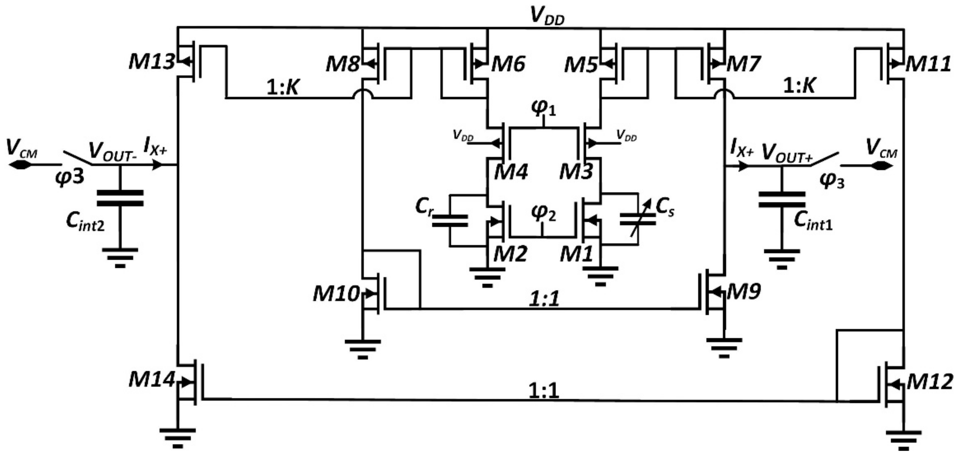
2. Analysis of the Differential CBCM

2.1. Working Principle

The schematic of fully differential CBCM amenable for fully integrated implementation, which was first proposed in [18,19], is reported in Figure 1. A couple of pseudo-inverters (M1, M3 and M2, M4) charge/discharge the sensing capacitor, Cs, and the reference capacitor, Cr. The pseudo-inverters are driven by clock phases φ1 and φ2, which are set to avoid short-circuit currents from VDD to ground, i.e., concurrent activation of transistors M1–M3 and M2–M4.
When clock phases φ1 and φ2 are low, Cs and Cr are charged through transistors M3 and M4. Current mirrors M5–M7, M6–M8 and M9–M10 enable subtraction of the instantaneous currents flowing in Cs, yielding
I X + ( t ) = I M 7 ( t ) I M 9 ( t ) = K C s d V C s d t C r d V C r d t
where K is the gain of current mirrors M5–M7 and M6–M8.
The current IX+ is averaged by capacitor C i n t 1 , yielding over one clock period, TS
I X + ¯ = 1 T s 0 T s I X + ( t ) d t = K T s 0 V D D V T P C s d V C s d t C r d V C r d t d t K Δ C V D D V T P T s
where VTP is the threshold voltage of transistors M5 and M6 and ΔC = CsCr. The rightmost approximation in Equation (2) holds considering that CS and Cr are charged to nearly VDD − |VTP| in one clock period.
The common mode voltage at the output of the CBCM circuit in Figure 1 is set to VCM by two auxiliary switches driven by the clock phase φ3 whose period, T3, should be sufficiently higher than Ts. Using Equation (2), the output voltage is expressed by
V o u t + = K Δ C V D D V T P T s T 3 C int 1
From Equation (3), it is apparent that by increasing the switching frequency or the supply voltage, the output voltage can be increased.
Due to circuit symmetry in Figure 1, we get IX+ = −IX and, consequently, Vout+ = −Vout (i.e., the differential output voltage is twice the value predicted by Equation (3)). When φ2 is high, the sensing and reference capacitors are discharged by M1 and M2. In this phase, PMOS of the pseudo-inverters are turned off, therefore the rest of the circuit is decoupled from the core and, neglecting leakage currents, the integration capacitors would maintain the charge gained during the previous clock cycle.

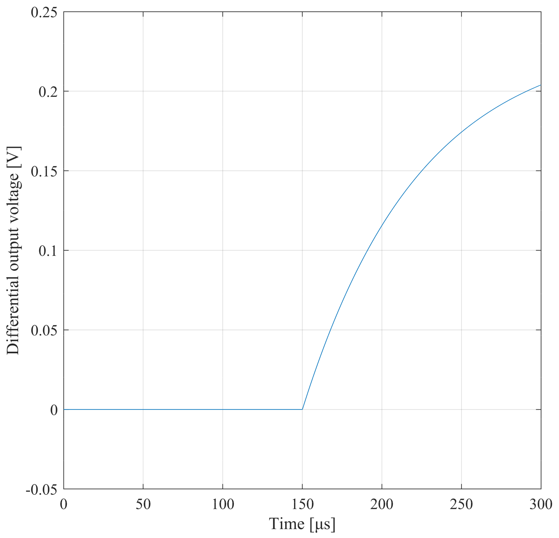
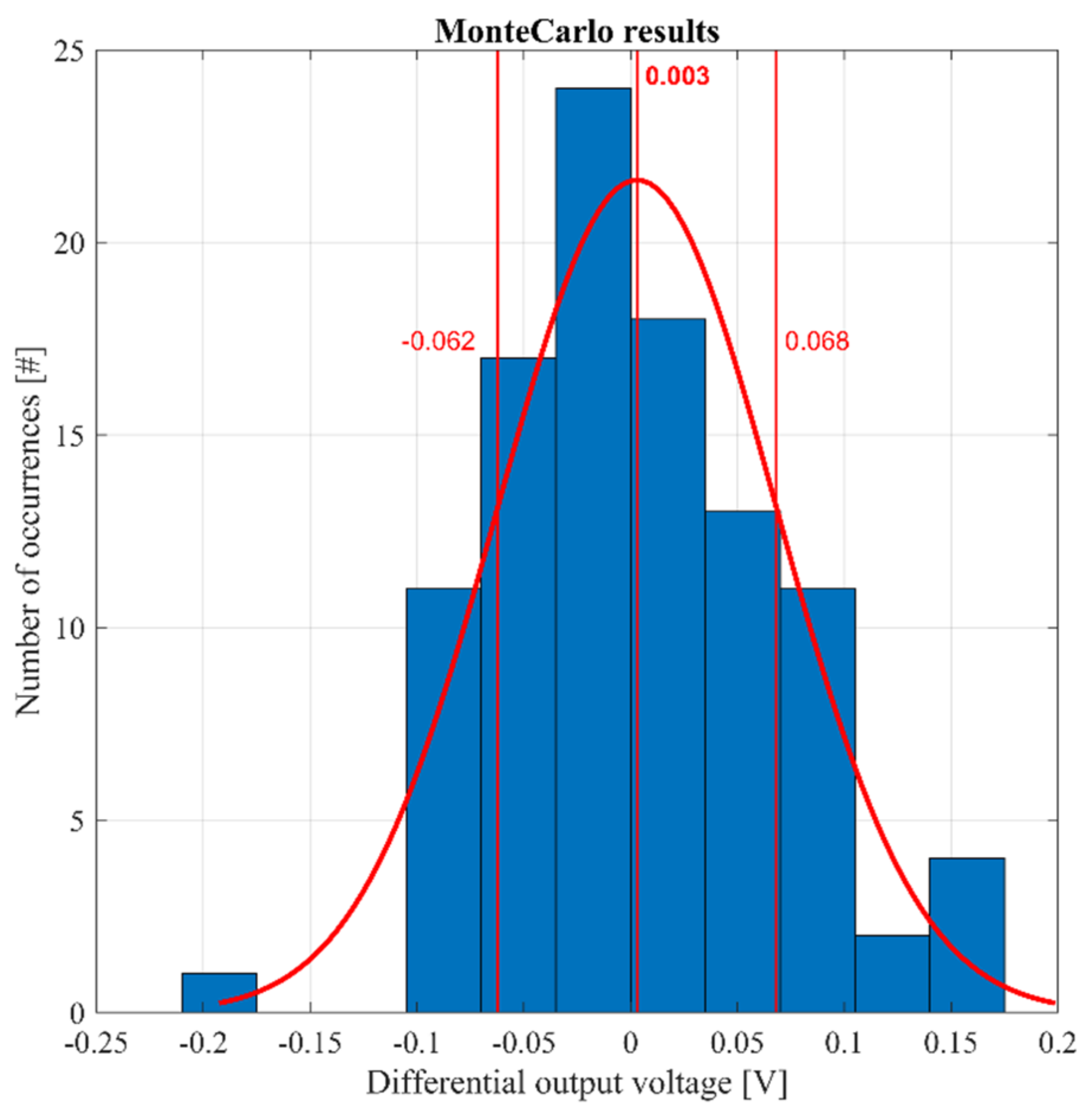
2.2. Simulation Results

The circuit in Figure 1 is designed and simulated using a standard 130-nm CMOS technology provided by STMicroelectronics. The supply voltage, switching period and common mode voltage is set equal to 3.3 V, 30 ns and 0.9 V, respectively. Although the nominal supply voltage of the adopted technology is 1.8 V, the high thickness field oxide devices are adopted for the circuit in order to increase the supply voltage to 3.3 V, which in turn allows increasing the output voltage level, as predicted by Equation (3). The common-mode voltage is fixed to 0.9 V, which is equal to half the supply voltage (equal to 1.8 V) of the comparator connected at the output of the circuit, which is not reported in this paper. The adopted main parameters for the circuit in Figure 1 are reported in Table 1. The absolute value of the reference and sensing capacitor plays a fundamental role in the circuit performance, but it cannot be freely set by the designer since it is related to the specific application. In our case, the circuit in Figure 1 is designed for a particulate matter detector where the value of Cs and Cr depends on the physical dimension of the capacitive electrode while the capacitance variation is in the order of tens of attofarads [21,22].
Figure 2 shows the differential output voltage, Vout+Vout, when a capacitance difference ∆C equal to 10 aF is applied at 150 μs. The figure confirms the behavior predicted by the analysis reported in Section 2.1.
Figure 3 compares the simulated transcharacteristic of the circuit in Figure 1 assuming T3 equal to 300 μs, with the theoretical values predicted through Equation (3). The simulated sensitivity is equal to 22 mV/aF.
The error between the two curves in Figure 3 is lower than 10% for ∆C ≤ 60 aF and increases up to 20% for higher capacitance difference values due to the nonlinearity of the simulated transcharacteristic. The nonlinear behavior of the circuit can be justified considering that the actual mirror current gain, K, is not constant but, due to the channel length modulation effect, is also a function of the output voltage Vout+ and Vout. Note that this effect regards all the current mirrors connected to the output nodes (i.e., M5–M7, M6–M13, M9–M10). The variation of the current mirror gain is therefore more pronounced for high values of ∆C, thus justifying the simulated behavior in Figure 3.
Note, however, that the non-linearity of the transcharacteristic in Figure 3 does not represent an issue in applications requiring the “activation” of a capacitive electrodes, like, as an example, airborne particle counters [10,11,12,21,22]. Nonetheless, the linearity of the circuit can be increased by adopting cascode current mirrors.
The critical issue of the CBCM system is the output offset caused by mismatch and process variations. Random mismatch variations can be evaluated by using the mismatch model in [23]:
σ Δ I D I D = σ Δ k k + g m I D σ Δ V t h
where σ Δ k k and σ Δ V t h are inversely proportional to the active area, while the ratio of gm and drain current is related to the transistor working region.
Regarding the mirrors, due to the very low charging currents, they are expected to work in the weak inversion saturated region. While the standard deviation of the variation of threshold can be minimized increasing the transistor area, the ratio between transconductance and drain current is the maximum, that is, a fundamental condition of the transistor operating in weak inversion. This condition leads to the conclusion that a residual mismatch is still caused by the subthreshold operating point even if the area is very high.
To better understand the effect of mismatches, let us consider, as an example, a mismatch between transistors M3 and M4 in Figure 1. In nominal condition (i.e., ∆C = 0), this mismatch will cause a charge difference, Q, during each switching cycle. If the charge flowing in M3 is bigger than that of M4, the integrating capacitor Cint1 accumulates more charge than Cint2, thus generating a differential output voltage offset expressed by
V d i f f , o f f s e t = 2 N Δ Q C int 1 , 2
where N is the number of clock cycles. According to the value of ∆Q and N, mismatch can cause an output voltage as high as the power supply. Of course, the same reasoning can be extended to any other couple of matched transistors.
As a confirmation of the analysis reported above, Figure 4 reports the Monte Carlo simulations over 100 runs of the differential output voltage of the traditional CBCM in Figure 1 assuming ∆C = 0 aF. It is apparent that the circuit shows standard deviation of the differential output voltage equal to about 1.35 V. Such a huge variation prevents the use of this simple topology unless a proper compensation strategy is adopted [17,19,20].

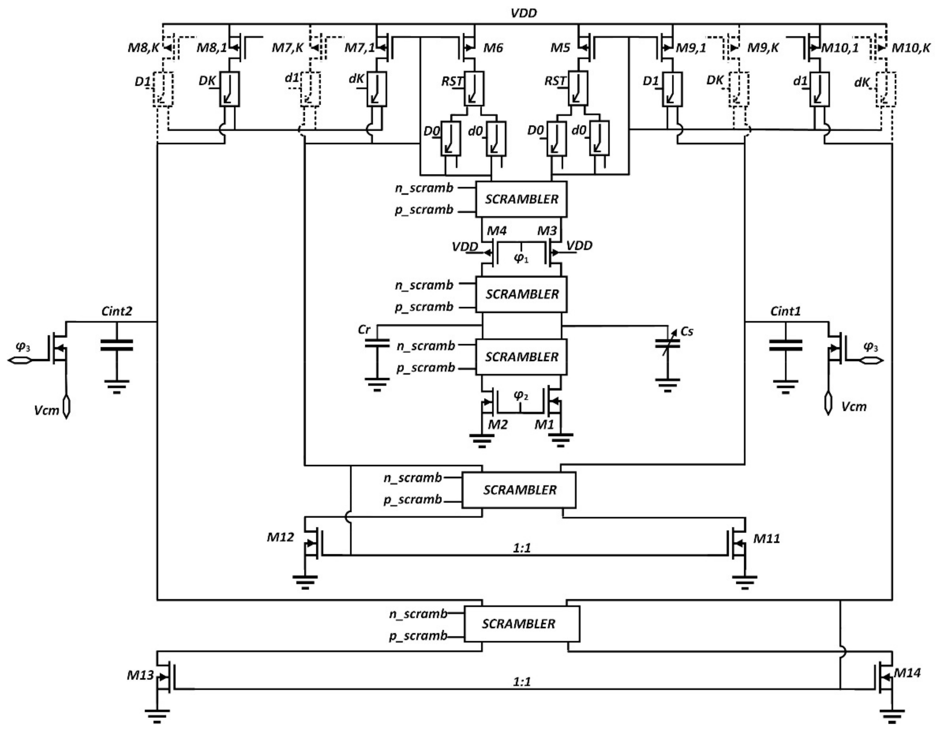
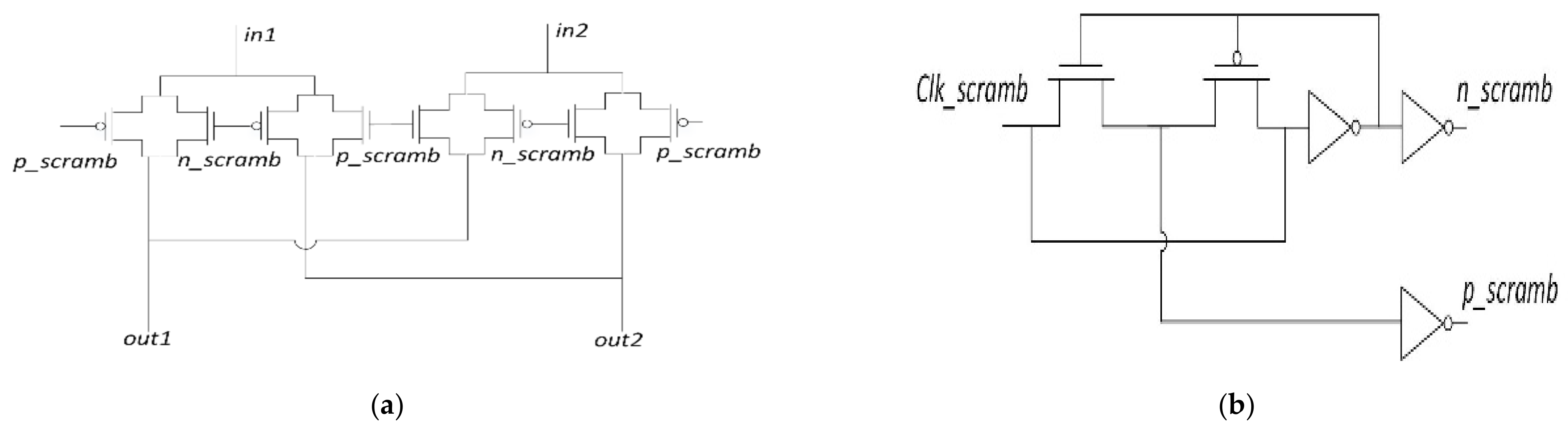
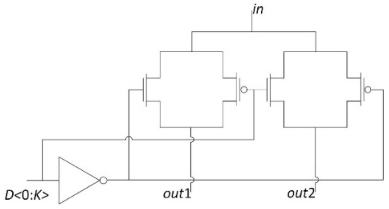
3. The Proposed Auto-Compensated CBCM Circuit

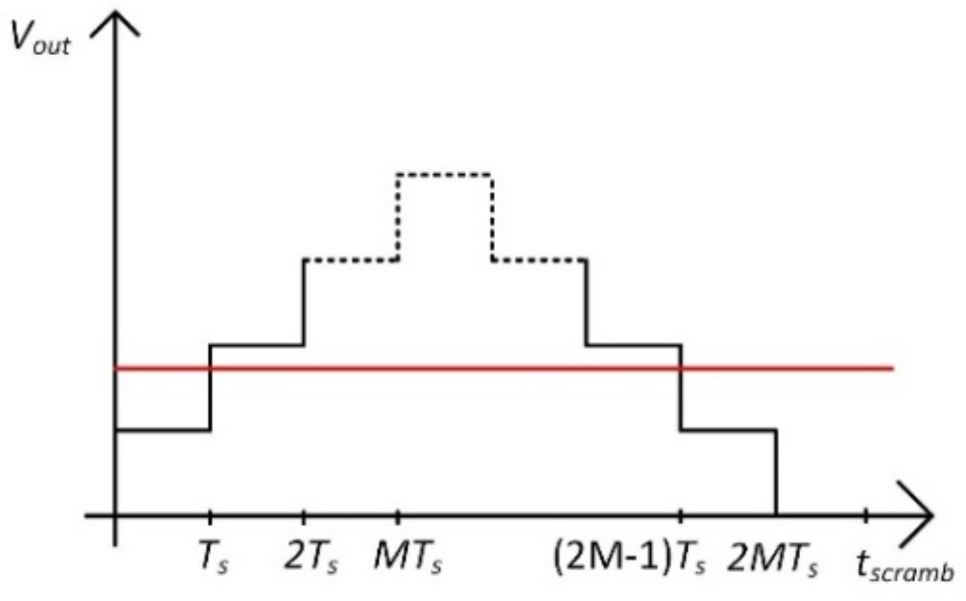
3.1. Working Principle

In order to decrease the standard deviation of the differential output voltage, an auto-compensated topology is proposed as shown in Figure 5. First of all, three ancillary blocks, called “scramblers”, have been added to the central core, to the reference and sensing capacitors and to the 1:1 mirrors. The scramblers are driven by two non-overlapping clock phases and periodically swap the drains of transistors, or the sensing and reference capacitors. In this way, in one semi period, the connection is the direct one (looking at the central core M1-Cs-M3), while in the second semi period, the connection is through M1-Cr-M3. Consequently, the mismatch current is averaged, thus reducing the equivalent offset.
Let us consider again, as an example, a mismatch between transistors M3 and M4 in nominal condition (i.e., ∆C = 0). By periodically swapping the drains of M3 and M4, the charge mismatch will be averaged over time. Assuming that the clock period of the scrambler, tscramb, is lower than the clock period, Ts, of the main phases φ1 and φ2, a simplified diagram of the differential output voltage is shown in Figure 6. It is worth noting that the principle of operation is like that of the chopping technique [24].
If the ratio tscramb/Ts is an integer number, M, it is apparent that if M3 and M4 are exchanged at the Mth main clock cycle, at the 2Mth clock cycle, the differential voltage is averaged and the offset to due mismatch is eliminated. In general, the differential voltage function is a growing and decreasing series of steps with an average value that increases as M increases, as shown in the following equation:
V o u t ¯ = a = 1 M / 2 2 a Δ Q C int 1 , 2 T s b = 1 M / 2 ( M 2 b ) Δ Q C int 1 , 2 T s t s c r a m b = a = 1 M / 2 2 a Δ Q b = 1 M / 2 M 2 b Δ Q M C int 1 , 2
Obviously, this reasoning can be applied to every pair of symmetrical transistors, thus reducing the total average error. Note, however, that the offset between the nominal values of Cs, Cr and Cint1, Cint2 must be compensated by an additional trimming circuit, like that proposed in [25].
The schematic of the scrambler is represented in Figure 7a, where the aspect ratios are 1 μm/0.5 μm and 3 μm/0.5 μm for NMOS and PMOS transistors, respectively. The scrambling circuit is basically a passive mixer driven by two 180° phase-shifted waves generated by the circuit in Figure 7b. When phase n_scramb is high, the central pair of transmission gates is open while the rightmost and leftmost part are a low impedance path, thus the classic connection of the CBCM. When phase p_scramb is high, the condition is the opposite, therefore the connections are swapped. The aspect ratios is 0.8 μm/0.5 μm for all transistors in Figure 7b.
To reduce the offset due to the mismatch of the 1:K current mirrors, an approach similar to the dynamical element matching (DEM) technique is adopted [26]. Each diode-connected transistor is periodically swapped with the other transistors of the current mirror. The schematic of the switch connected to the drains of the transistors of the 1:K current mirrors is shown in Figure 8, where the aspect ratios are 2.4 μm/0.5 μm and 0.8 μm/0.5 μm for NMOS and PMOS transistors, respectively. The 10-bit binary word D < 0:K > is made up by a series of zeroes with only a “1” that moves cyclically from the right to the left and is generated by a finite state machine (FSM). When the signal D1 is high, the rightmost transmission gate is a low impedance path therefore, taking in account the M5-M9 mirror, the M9,1 PMOS exchanges with the diode connected. In the third period, the diode connected MOS is exchanged with the second PMOS M9,2, etc. In the first state, when D0 is high, the situation is the classical one. In this way, the mismatch of a mirror is reduced, producing an average offset much smaller than the uncompensated version.
The diode connected PMOS overhangs a combination of three scramblers, because the diode connected PMOS in a first phase is exchanged with the PMOSs that overhang the output node, then with the PMOSs that overhang the diode connected NMOS (therefor, two different FSM that are set and reset by two signal in phase opposition). The parallel of the two scramblers under the principal one are unable/enabled by the reset signal of the memory part of the FSM.

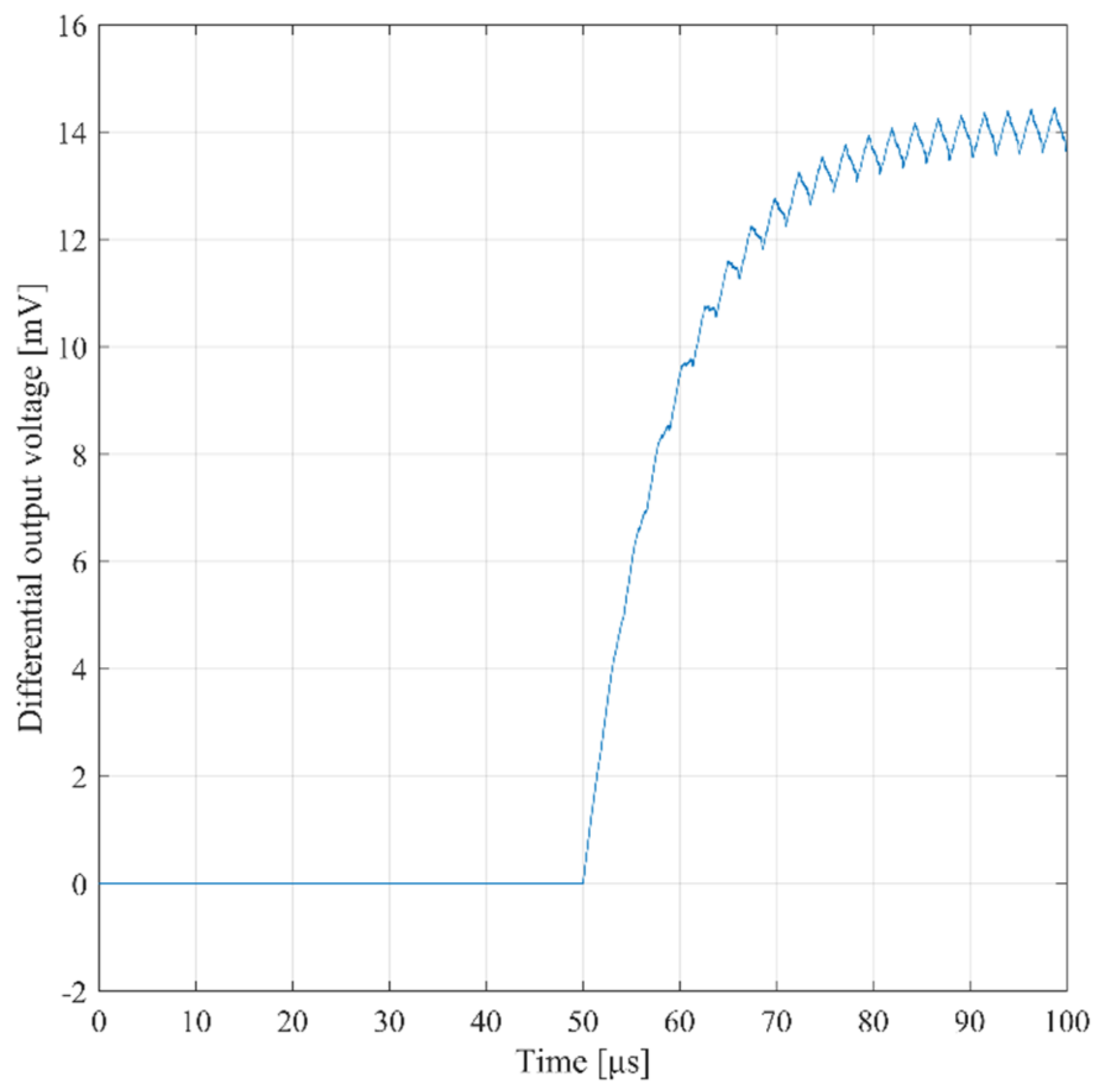
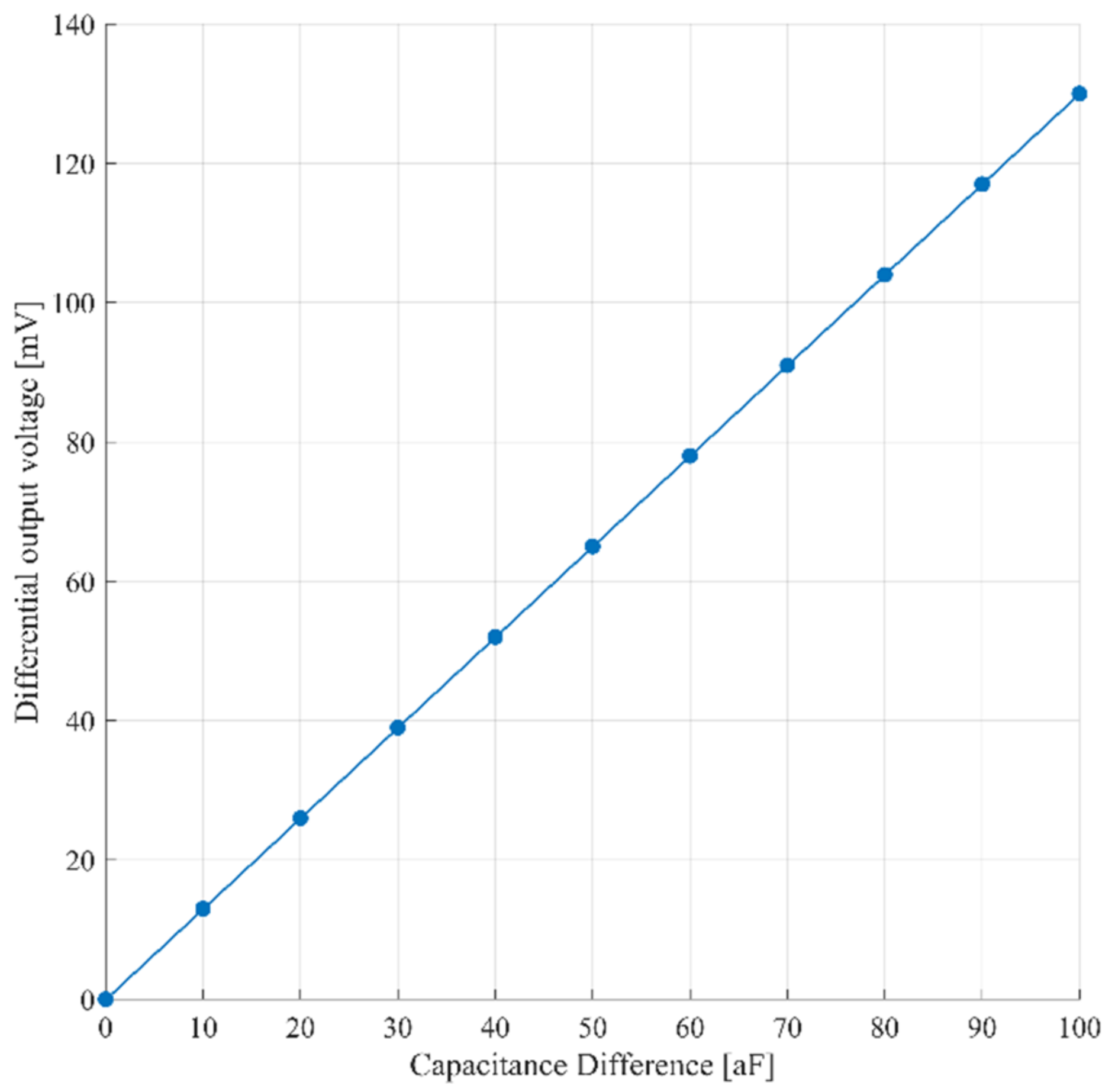
3.2. Simulation Results

The proposed circuit in Figure 5 has been simulated using the same parameters reported in Figure 1. The switching period of the scramblers is set equal to 600 ns (i.e., M = 20 in Equation (6)). The FSM clock period is set equal to 60 ns.
Figure 9 shows the differential output voltage, Vout+Vout−, when a capacitance difference ∆C equal to 10 aF is applied at 50 μs. As compared to the traditional solution, the output voltage variation is reduced. This is due to the effect of the transistors implementing the switches of the scramblers and the DEM circuit that cause a reduction of the charging current into the integrating capacitors. The magnitude of the ripple in Figure 9 is due to the scramblers and, in particular, to the DEM applied to the current mirrors. This ripple can either be reduced by degenerating the mirror devices or trimming it before doing DEM. Alternatively, DEM ripple can also be suppressed by an additional low pass filter.
Figure 10 reports the transcharacteristic of the circuit in Figure 5 assuming T3 is equal to 100 μs. The sensitivity is equal to 1.3 mV/aF, therefore it is 17 times lower than that of the traditional solution.
Finally, Figure 11 reports the Monte Carlo simulations over 100 runs of the differential output voltage of the proposed circuit assuming ∆C = 0 aF. It can be noted that now the standard deviation has been reduced to about 65 mV, which is about 20 times lower than that of the traditional solution.

4. Conclusions

In this paper an automatic offset cancellation topology is proposed to improve the performance of the differential CBCM. The proposed circuit allows reducing the offset of the output voltage due to mismatches in an automatic way by exploiting scramblers and DEM technique. Simulation results shows the effectiveness of the proposed strategy, which allows a 20× reduction of the standard deviation, but with a 14× reduction of the sensitivity. The performance increase, moreover, is paid by additional area occupation and circuit complexity, but it is worth noting that the offset is automatically and continuously reduced without human intervention, thus enabling the adoption of the CBCM topology in those applications where hundreds of capacitive electrodes must be processed in parallel.

Author Contributions

Conceptualization, A.D.G., U.F., M.V.; formal analysis, A.D.G., U.F., M.V., G.B.; data curation, U.F.; formal analysis, A.D.G., U.F., M.V.; writing—original draft preparation, A.D.G. and U.F.; writing—review and editing, A.D.G., U.F., M.V., G.B.; visualization, A.D.G. and U.F.; supervision, A.D.G. and G.B. All authors have read and agreed to the published version of the manuscript.

Funding

This research received no external funding.

Institutional Review Board Statement

Not applicable.

Conflicts of Interest

The authors declare no conflict of interest.

References

  1. Ferlito, U.; Grasso, A.D.; Pennisi, S.; Vaiana, M.; Bruno, G. Sub-Femto-Farad Resolution Electronic Interfaces for Integrated Capacitive Sensors: A Review. IEEE Access 2020, 8, 153969–153980. [Google Scholar] [CrossRef]
  2. Valente, V.; Demosthenous, A. A 32-by-32 CMOS microelectrode array for capacitive biosensing and impedance spectroscopy. In Proceedings of the 2017 IEEE International Symposium on Circuits and Systems (ISCAS), Baltimore, MD, USA, 28–31 May 2017; pp. 1–4. [Google Scholar] [CrossRef] [Green Version]
  3. Couniot, N.; Francis, L.A.; Flandre, D. A 16 x 16 CMOS Capacitive Biosensor Array Towards Detection of Single Bacterial Cell. IEEE Trans. Biomed. Circuits Syst. 2016, 10, 364–374. [Google Scholar] [CrossRef] [PubMed]
  4. Carminati, M.; Ferrari, G.; Vahey, M.D.; Voldman, J.; Sampietro, M. Miniaturized Impedance Flow Cytometer: Design Rules and Integrated Readout. IEEE Trans. Biomed. Circuits Syst. 2017, 11, 1438–1449. [Google Scholar] [CrossRef] [PubMed]
  5. Senevirathna, B.P.; Lu, S.; Dandin, M.P.; Basile, J.; Smela, E.; Abshire, P.A. Real-Time Measurements of Cell Proliferation Using a Lab-on-CMOS Capacitance Sensor Array. IEEE Trans. Biomed. Circuits Syst. 2018, 12, 510–520. [Google Scholar] [CrossRef] [PubMed]
  6. Laborde, C.; Pittino, F.; Verhoeven, H.A.; Lemay, S.J.G.; Selmi, L.; Jongsma, M.A.; Widdershoven, F.P. Real-time imaging of microparticles and living cells with CMOS nanocapacitor arrays. Nat. Nanotechnol. 2015, 10, 791–795. [Google Scholar] [CrossRef] [PubMed] [Green Version]
  7. Wang, Y.; Fu, Q.; Zhang, Y.; Zhang, W.; Chen, D.; Yin, L.; Liu, X. A Digital Closed-Loop Sense MEMS Disk Resonator Gyroscope Circuit Design Based on Integrated Analog Front-end. Sensors 2020, 20, 687. [Google Scholar] [CrossRef] [PubMed] [Green Version]
  8. Aaltonen, L.; Kalanti, A.; Pulkkinen, M.; Paavola, M.; Kamarainen, M.; Halonen, K.A.I. A 2.2 mA 4.3 mm2 ASIC for a 1000°/s 2-Axis Capacitive Micro-Gyroscope. IEEE J. Solid State Circuits 2011, 46, 1682–1692. [Google Scholar] [CrossRef]
  9. Ferlito, U.; Grasso, A.D.; Vaiana, M.; Bruno, G. Sub-fF Resolution Capacitive Amplifier for Particulate Matter Airborne Detection. In Proceedings of the 2020 International Conference on Electrical, Communication, and Computer Engineering (ICECCE), Istanbul, Turkey, 13 June 2020; pp. 1–4. [Google Scholar] [CrossRef]
  10. Ciccarella, P.; Carminati, M.; Sampietro, M.; Ferrari, G. Multichannel 65 zF rms Resolution CMOS Monolithic Capacitive Sensor for Counting Single Micrometer-Sized Airborne Particles on Chip. IEEE J. Solid State Circuits 2016, 51, 2545–2553. [Google Scholar] [CrossRef]
  11. Evans, I.; York, T. Microelectronic Capacitance Transducer for Particle Detection. IEEE Sens. J. 2004, 4, 364–372. [Google Scholar] [CrossRef]
  12. Ferlito, U.; Grasso, A.D.; Vaiana, M. Bruno, Integrated Airborne Particle Matter Detector. In Proceedings of the 2019 26th IEEE International Conference on Electronics, Circuits and Systems (ICECS), Genoa, Italy, 27 November 2019; pp. 95–96. [Google Scholar] [CrossRef]
  13. Chen, J.C.; McGaughy, B.W.; Sylvester, D.; Hu, C. An on-chip, attofarad interconnect charge-based capacitance measurement (CBCM) technique. In Proceedings of the International Electron Devices Meeting, Technical Digest, San Francisco, CA, USA, 8–11 December 1996; pp. 69–72. [Google Scholar] [CrossRef]
  14. Sylvester, D.; Chen, J.C.; Hu, C. Investigation of interconnect capacitance characterization using charge-based capacitance measurement (CBCM) technique and three-dimensional simulation. IEEE J. Solid State Circuits 1998, 33, 449–453. [Google Scholar] [CrossRef]
  15. Vendrame, L.; Bortesi, L.; Cattane, F.; Bogliolo, A. Crosstalk-Based Capacitance Measurements: Theory and Applications. IEEE Trans. Semicond. Manufact. 2006, 19, 67–77. [Google Scholar] [CrossRef]
  16. Forouhi, S.; Dehghani, R.; Ghafar-Zadeh, E. Toward High Throughput Core-CBCM CMOS Capacitive Sensors for Life Science Applications: A Novel Current-Mode for High Dynamic Range Circuitry. Sensors 2018, 18, 3370. [Google Scholar] [CrossRef] [PubMed] [Green Version]
  17. Ghafar-Zadeh, E.; Sawan, M. A Hybrid Microfluidic/CMOS Capacitive Sensor Dedicated to Lab-on-Chip Applications. IEEE Trans. Biomed. Circuits Syst. 2007, 1, 270–277. [Google Scholar] [CrossRef] [PubMed]
  18. Prakash, S.B.; Abshire, P. A Fully Differential Rail-to-Rail Capacitance Measurement Circuit for Integrated Cell Sensing. In Proceedings of the 2007 IEEE Sensors, Atlanta, GA, USA, 28–31 October 2007; pp. 1444–1447. [Google Scholar] [CrossRef]
  19. Prakash, S.B.; Abshire, P. A Fully Differential Rail-to-Rail CMOS Capacitance Sensor with Floating-Gate Trimming for Mismatch Compensation. IEEE Trans. Circuits Syst. I 2009, 56, 975–986. [Google Scholar] [CrossRef]
  20. Ghafar-Zadeh, E.; Sawan, M.; Chodavarapu, V.P.; Hosseini-Nia, T. Bacteria Growth Monitoring Through a Differential CMOS Capacitive Sensor. IEEE Trans. Biomed. Circuits Syst. 2010, 4, 232–238. [Google Scholar] [CrossRef] [PubMed]
  21. York, T.A.; Evans, I.G.; Pokusevski, Z.; Dyakowski, T. Particle detection using an integrated capacitance sensor. Sens. Actuators A Phys. 2001, 92, 74–79. [Google Scholar] [CrossRef]
  22. Ferlito, U.; Grasso, A.D.; Vaiana, M.; Bruno, G. A Time-Based Electronic Front-End for a Capacitive Particle Matter Detector. Sensors 2021, 21, 1840. [Google Scholar] [CrossRef] [PubMed]
  23. Croon, J.A.; Rosmeulen, M.; Decoutere, S.; Sansen, W.; Maes, H.E. An easy-to-use mismatch model for the MOS transistor. IEEE J. Solid State Circuits 2002, 37, 1056–1064. [Google Scholar] [CrossRef]
  24. Enz, C.C.; Temes, G.C. Circuit techniques for reducing the effects of op-amp imperfections: Autozeroing, corelated double sampling and chopper stabilization. Proc. IEEE 1996, 84, 1584–1614. [Google Scholar] [CrossRef] [Green Version]
  25. Grasso, A.D.; Vaiana, M.G.G.; Bruno, G. Area-optimized sub-fF offset trimming circuit for capacitive MEMS interfaces. In Proceedings of the ECCTD 2017, Catania, Italy, 4–6 September 2017; pp. 1–4. [Google Scholar] [CrossRef]
  26. Van de Plassche, R.J. Dynamic element matching for high-accuracy monolithic D/A converters. IEEE J. Solid State Circuits 1976, 11, 795–800. [Google Scholar] [CrossRef]
Figure 1. Schematic of the differential CBCM structure.
Jlpea 11 00022 g001
Figure 2. Simulated differential output voltage of the traditional CBCM in Figure 1 with ∆C = 10 aF at 150 μs.
Jlpea 11 00022 g002
Figure 3. Transcharacteristic of the traditional CBCM in Figure 1.
Jlpea 11 00022 g003
Figure 4. Monte Carlo simulation results for the circuit in Figure 1.
Jlpea 11 00022 g004
Figure 5. Schematic of the proposed auto-compensated CBCM circuit.
Jlpea 11 00022 g005
Figure 6. Output voltage over one period of the clock of the scrambler.
Jlpea 11 00022 g006
Figure 7. (a) Schematic of the scrambler circuit; (b) schematic of the scrambler phase generator.
Jlpea 11 00022 g007
Figure 8. Schematic of the switch connected to the drains of the transistors of the 1:K current mirrors.
Jlpea 11 00022 g008
Figure 9. Simulated differential output voltage of the proposed circuit in Figure 5 with ∆C = 10 aF at 50 μs.
Jlpea 11 00022 g009
Figure 10. Transcharacteristic of the proposed CBCM in Figure 5.
Jlpea 11 00022 g010
Figure 11. Monte Carlo simulation results for the circuit in Figure 5.
Jlpea 11 00022 g011
Table 1. Main parameters of the circuit in Figure 1.
ParameterValue
M1, M21 µm/0.5 µm
M3, M43 µm/0.5 µm
M5, M6, M7, M8, M11, M132 µm/2 µm
M9, M10, M12, M145 µm/10 µm
K2
Cint1,25 pF
Cs,r1 fF
Publisher’s Note: MDPI stays neutral with regard to jurisdictional claims in published maps and institutional affiliations.

