Article

Energy-Efficient Non-Von Neumann Computing Architecture Supporting Multiple Computing Paradigms for Logic and Binarized Neural Networks

Dipartimento di Ingegneria “Enzo Ferrari”, Università di Modena e Reggio Emilia, Via P. Vivarelli 10/1, 41125 Modena, Italy
*
Author to whom correspondence should be addressed.
J. Low Power Electron. Appl. 2021, 11(3), 29; https://0-doi-org.brum.beds.ac.uk/10.3390/jlpea11030029
Submission received: 31 May 2021 / Revised: 23 June 2021 / Accepted: 30 June 2021 / Published: 6 July 2021
(This article belongs to the Special Issue Low Power Memory/Memristor Devices and Systems)

Abstract

:
Different in-memory computing paradigms enabled by emerging non-volatile memory technologies are promising solutions for the development of ultra-low-power hardware for edge computing. Among these, SIMPLY, a smart logic-in-memory architecture, provides high reconfigurability and enables the in-memory computation of both logic operations and binarized neural networks (BNNs) inference. However, operation-specific hardware accelerators can result in better performance for a particular task, such as the analog computation of the multiply and accumulate operation for BNN inference, but lack reconfigurability. Nonetheless, a solution providing the flexibility of SIMPLY while also achieving the high performance of BNN-specific analog hardware accelerators is missing. In this work, we propose a novel in-memory architecture based on 1T1R crossbar arrays, which enables the coexistence on the same crossbar array of both SIMPLY computing paradigm and the analog acceleration of the multiply and accumulate operation for BNN inference. We also highlight the main design tradeoffs and opportunities enabled by different emerging non-volatile memory technologies. Finally, by using a physics-based Resistive Random Access Memory (RRAM) compact model calibrated on data from the literature, we show that the proposed architecture improves the energy delay product by >103 times when performing a BNN inference task with respect to a SIMPLY implementation.

1. Introduction

The demand for more ubiquitous edge computing promoted by the rapidly growing volume of data exchanged over the communication network by devices for the Internet of Things (IoT) requires the development of more energy-efficient computing architectures [1,2]. Accordingly, several new computing paradigms [3,4,5,6,7,8,9,10] have been proposed, encouraging a departure from the traditional von Neumann architecture. All these new computing approaches aim at performing computation directly inside the memory by exploiting novel emerging non-volatile memory (ENVM) technologies, therefore bypassing the main performance bottleneck of traditional von Neumann architectures, i.e., the communication between the memory and the processing unit over a slow bus. While operation specific hardware accelerators can achieve very high performance when executing a specific task, the possibility to reconfigure the type of operations computed in-memory may benefit resource-constrained devices for edge computing applications [11]. Among in-memory computing paradigms providing reconfigurability [4,12,13,14,15,16], architectures based on resistive memory devices and the material implication (IMPLY) logic are a promising solution [13]. Also, a smart IMPLY (SIMPLY) [17] architecture was proposed for solving the reliability issues of conventional IMPLY-based architectures demonstrating high reliability and high energy efficiency when implementing logic operations. Recently, a binarized neural network (BNN) [18] implementation based on the SIMPLY architecture was proposed [19,20] and shown to improve energy efficiency with respect to conventional embedded system implementations. Nevertheless, specific BNN hardware accelerators based on resistive memory technologies [21,22,23,24,25] which accelerate in analog the multiply and accumulate (MAC) operation can achieve higher performance if properly designed, lacking, however, reconfigurability options. Thus, a solution enabling the coexistence of both computing approaches on the same resources would enable the development of reconfigurable ultra-low-power edge computing hardware, but such a solution is still missing.
In this work, we design a new in-memory computing architecture enabling the coexistence on the same 1T1R crossbar array of both the SIMPLY logic-in-memory paradigm and the analog acceleration of the multiply and accumulate operation for BNN inference applications. We analyze the design tradeoffs of the proposed architecture and indicate the opportunities and limitations introduced using different emerging non-volatile memory technologies. Finally, exploiting a physics-based Resistive Random Access Memory (RRAM) compact model calibrated on a TiN/HfOx/AlOx/Pt RRAM technology from the literature [26], we benchmark with respect to a SIMPLY implementation the performance improvements for an inference task on a BNN provided by the novel architecture.

2. Results

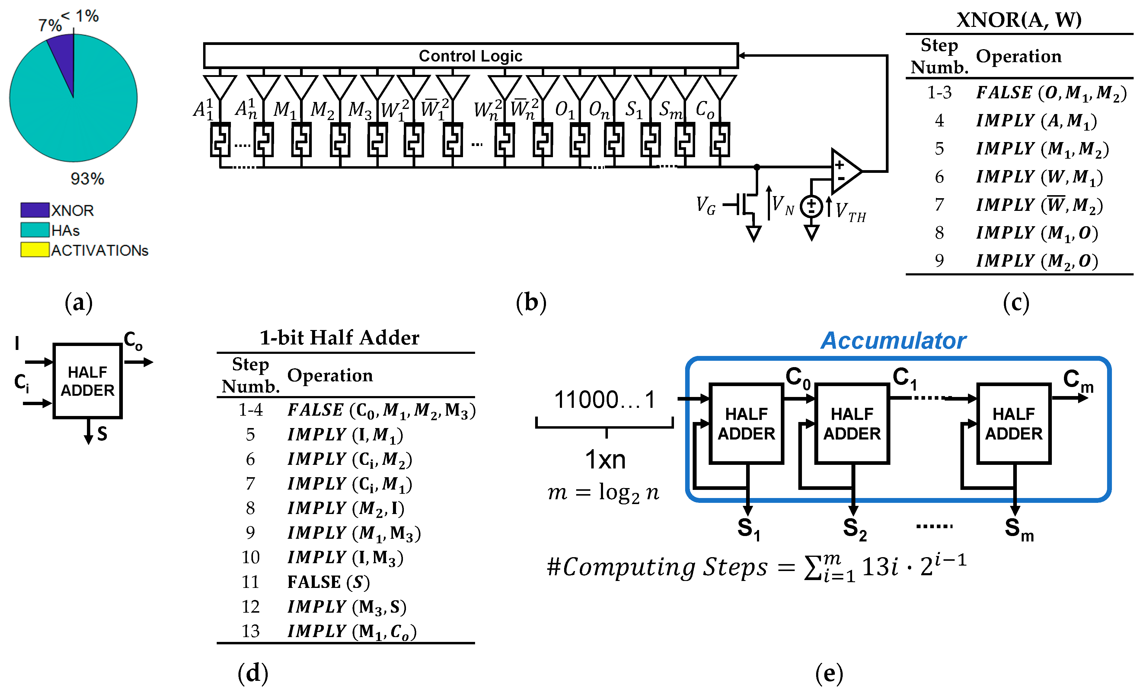
2.1. Logic-in-Memory and the SIMPLY Architecture

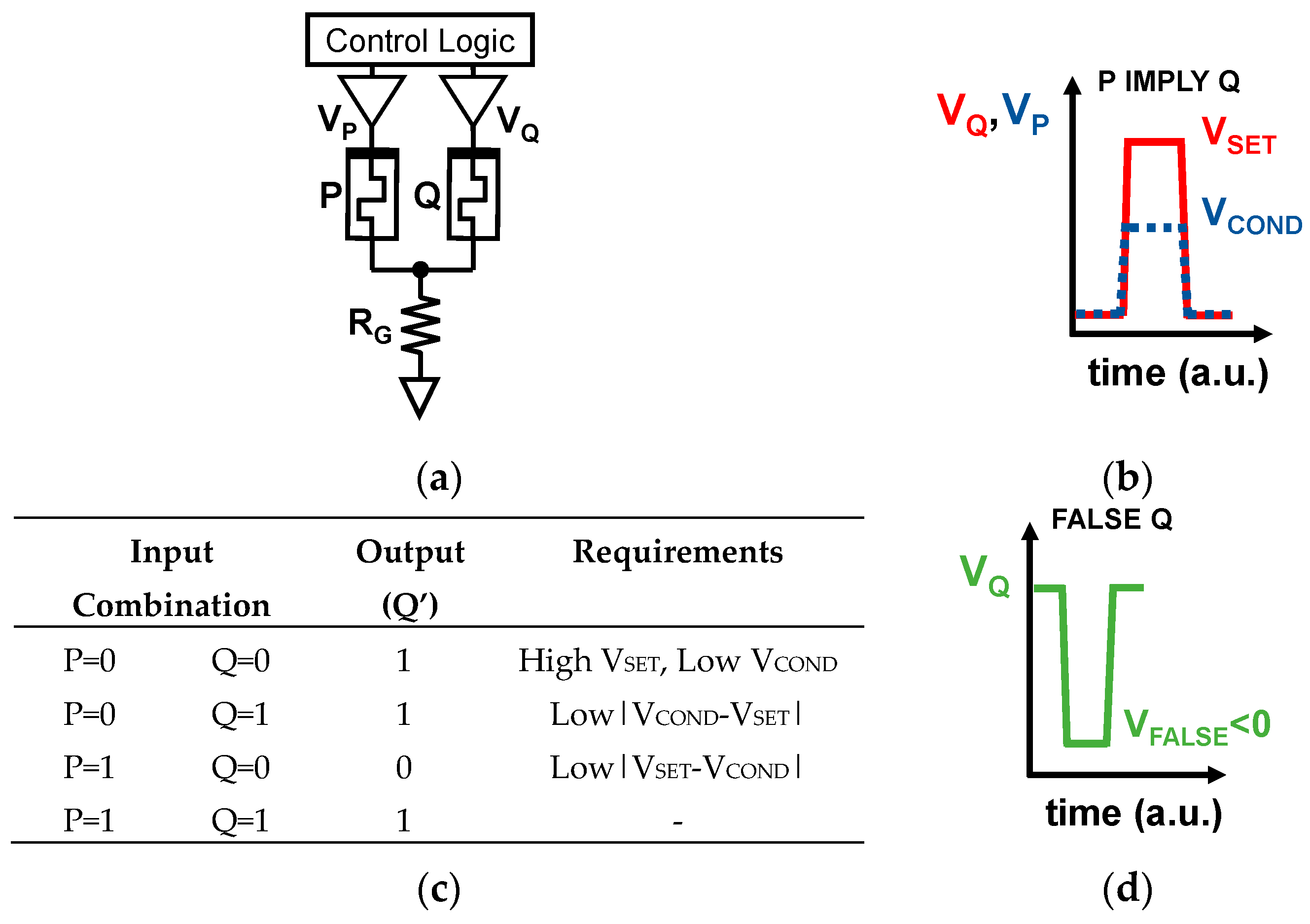
2.1.1. Material Implication Logic
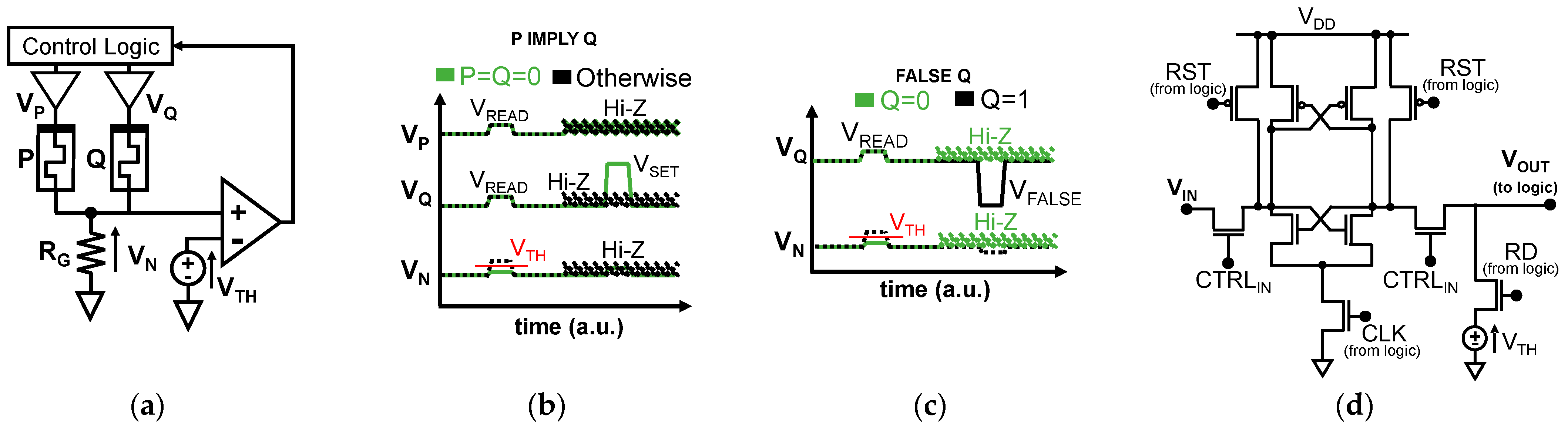
The IMPLY logic is based on two logic operations, i.e., the IMPLY, the truth table of which is shown in Figure 1c, and the FALSE which always results in a logic zero. These two operations can be implemented with RRAM devices and the circuit shown in Figure 1a, which comprises a resistor (i.e., RG in Figure 1a), a control logic and analog tri-state buffers to deliver appropriate voltages to RRAM devices. Since the IMPLY and the FALSE form a complete logic group, all logic operations can be implemented with a sequence of these two operations [27]. In this framework, logic bits are mapped to RRAM devices resistances, and a logic 0 and a logic 1 are encoded into a high-resistive state (HRS) or low-resistive state (LRS), respectively. When performing computations RRAMs act at the same time both as the inputs and the outputs of computation. In particular, to perform an IMPLY operation between two bits (i.e., P and Q in Figure 1b,c), the control logic simultaneously drives the top electrodes of the two input RRAM devices with two voltage pulses with amplitudes VCOND and VSET (see Figure 1b) on the two devices, respectively. By determining an appropriate value for VSET and VCOND voltages, which must satisfy all the different requirements for each input combinations reported in Figure 1c, the state of the device receiving VCOND (i.e., P in Figure 1b,c) never changes while the state of the other device (i.e., Q in Figure 1b,c) changes according to the IMPLY truth table (see Figure 1c, where Q’ is the state of Q after the IMPLY operation execution). The FALSE operation is executed by applying a negative voltage pulse with amplitude VFALSE to a single device to reset it into a HRS (see Figure 1d). However, this IMPLY scheme is affected by several reliability challenges, such as logic state degradation and small tolerance to voltage variations, which hinder its implementation [28,29].

2.1.2. SIMPLY

A solution to the reliability issues affecting the conventional IMPLY architecture is the SIMPLY architecture [17]. In SIMPLY, the computation of the IMPLY operation is split into two steps, i.e., a read step and a conditional write step. As shown in the IMPLY truth table (see Figure 1c), the state of Q, which is the device storing the result of the IMPLY operation, changes only when both P and Q (i.e., the inputs of the IMPLY operation) are in HRS. This condition can be detected by applying two simultaneous small read voltage pulses with amplitude VREAD to P and Q and comparing the voltage across RG (VN) with a threshold (VTH) using a comparator, as shown in Figure 2a. In fact, VN is lower when both inputs are zero than in all the other cases (see Figure 2b), providing a sufficient read margin (RM) for the comparator. The output of the comparator is fed to a control logic which then pulses VSET on Q only when necessary. By using a sufficiently low VREAD voltage the problem of logic state degradation is effectively solved [17]. Also, the drivers in the peripheral circuitry of the array can be simplified, as VCOND is no longer required. In addition, the high VSET voltage pulse is applied only in the first case of the truth table, while in the other three cases the main energy consumption is due to the small VREAD pulses and the comparator. As described in previous works [19,20], the latter can be implemented with the voltage sense amplifier (VSA) in Figure 2d, which is fast and energy efficient (i.e., the VSA implemented with a 45 nm technology from [30], and a VDD of 2V dissipated just 8 fJ per comparison on average). Therefore, SIMPLY considerably improves the energy per IMPLY operation in three out of four cases of the truth table compared to the conventional IMPLY architecture [17,19].
To further improve the energy efficiency, the same approach can be used for the FALSE operation [19,20]. When a device is in HRS the high VFALSE voltage results in unnecessary energy dissipation. This can be prevented by first reading the state of the device and then applying the VFALSE only when the device is in LRS (see Figure 2c). The effectiveness in reducing the energy per operation depends on the employed RRAM technology [19]. In fact, the achieved energy reduction with RRAM technology characterized by very high HRS is limited, while it is relevant for technologies with relatively low HRS.
The RM is the most important reliability metric, and enough RM must be ensured even in presence of resistive state variability and random telegraph noise (RTN). While a higher RM can be achieved by slightly increasing VREAD (see Figure 3a), a higher RM is also obtained by using the optimal value for RG (see Figure 3b) that is determined using equation (1) from [31], where RHRS,MAX and RHRS,MIN are the ±3σ values of the RHRS distribution, while RLRS,MAX is the +3σ value of the RLRS distribution.
R G = 1 1 R H R S M A X + 1 R L R S M A X R H R S M I N 2 ,
The SIMPLY framework can be implemented also on crossbar arrays [19]. Specifically, to implement SIMPLY on the 1T1R crossbar array the architecture shown in Figure 4 is needed. Additional field effect transistor (FET) devices in the array periphery are used to connect adjacent rows of the crossbar to perform IMPLY operations between devices on the same column but different rows, and to select specific rows. Also, the degree of parallelism in the SIMPLY architecture can be increased by adding more VSAs in the array periphery, as shown in Figure 4. Using multiple VSAs enables the realization of single instruction multiple data (SIMD) architectures, in which the IMPLY and FALSE operations can be performed in parallel on data stored in different rows but aligned on the same columns. For instance, to perform IMPLY operations in parallel, two columns are driven with the read voltage, then only the FETs implementing RG and those enabling the selected rows are enabled, therefore routing each active row to the specific VSA. The control logic receives in input the results of all the comparisons and activates only the rows where an RRAM device should be switched during the device SET step. As shown in previous works [19,31], the use of SIMPLY-based SIMD architectures results in high computing efficiency and throughput.

2.2. Binarized Neural Networks (BNNs) Hardware Accelerator Architectures

2.2.1. Binarized Neural Networks with SIMPLY

BNNs are an effective solution that enables the implementation of neural networks at a lower computational cost, while retaining sufficiently high accuracies [18], as compared to full-precision neural networks. In fact, by using 1-bit weights and activations only logic operations are required to perform an inference task. Thanks to this simplification, previous works [19,20] showed how BNN inference can be implemented in the SIMPLY computing framework. The network parameters are trained offline using for example the DoReFa-Net algorithm [32] (see Section 4.2) and directly mapped to the resistance of RRAM devices in the crossbar array, as shown in Figure 5b where a single crossbar row is reported. In BNNs, the multiply and accumulate (MAC) can be implemented with bitwise XNOR operations between each neuron weights and input activations, the accumulation with the popcount operation, and each neuron activation by performing a comparison with a trained threshold. Finally, the output class is predicted by using the hardmax function, which selects the class corresponding to the neuron with the highest output activation. By enabling the realization of SIMD architectures, the resulting SIMPLY implementation exploits the intrinsic parallelism in BNN computations, to efficiently compute in parallel the operations in each neural network layer. Also, thanks to its reconfigurability, SIMPLY enables the possibility to easily implement different neural networks topologies. However, the high degree of reconfigurability comes at the price of a high number of computing steps, which limits the latency performance. Specifically, among the different operations, the computation of MAC operations is the main limitation in SIMPLY-based BNN implementations, and accounts for almost all the computing steps of a network layer when considering a layer with 1000 input activations, as shown in Figure 5a. While each bitwise XNOR requires nine computing steps (see Figure 5c), the number per accumulation operations for the implemented accumulator rapidly rises as the number of inputs to a network layer increases. In fact, to implement the accumulator, a chain of half-adders (HAs) is used where the first HA is fed its current output and the bit to be accumulated, while the following HAs are fed their current output and the carry-out from the previous HA in the chain [19,20], as shown in Figure 5e. Each HA requires 13 computing steps to accumulate a single bit (see Figure 5d). Thus, the whole accumulation operation is computed in m i = 1 13 i · 2 ( i 1 ) . This is because each HA is activated only after a number of input bits equal to two to the power of their respective bit position has been accumulated, since the carry-out bits from the preceding HA stage is necessarily zero when fewer bits have been accumulated. Therefore, the latency for computing the accumulation operation rises exponentially when the size of a neural network layer increases, thus suggesting that BNN SIMPLY implementations are more suitable for small neural network implementations, while the implementation of larger networks would require more efficient MAC execution.

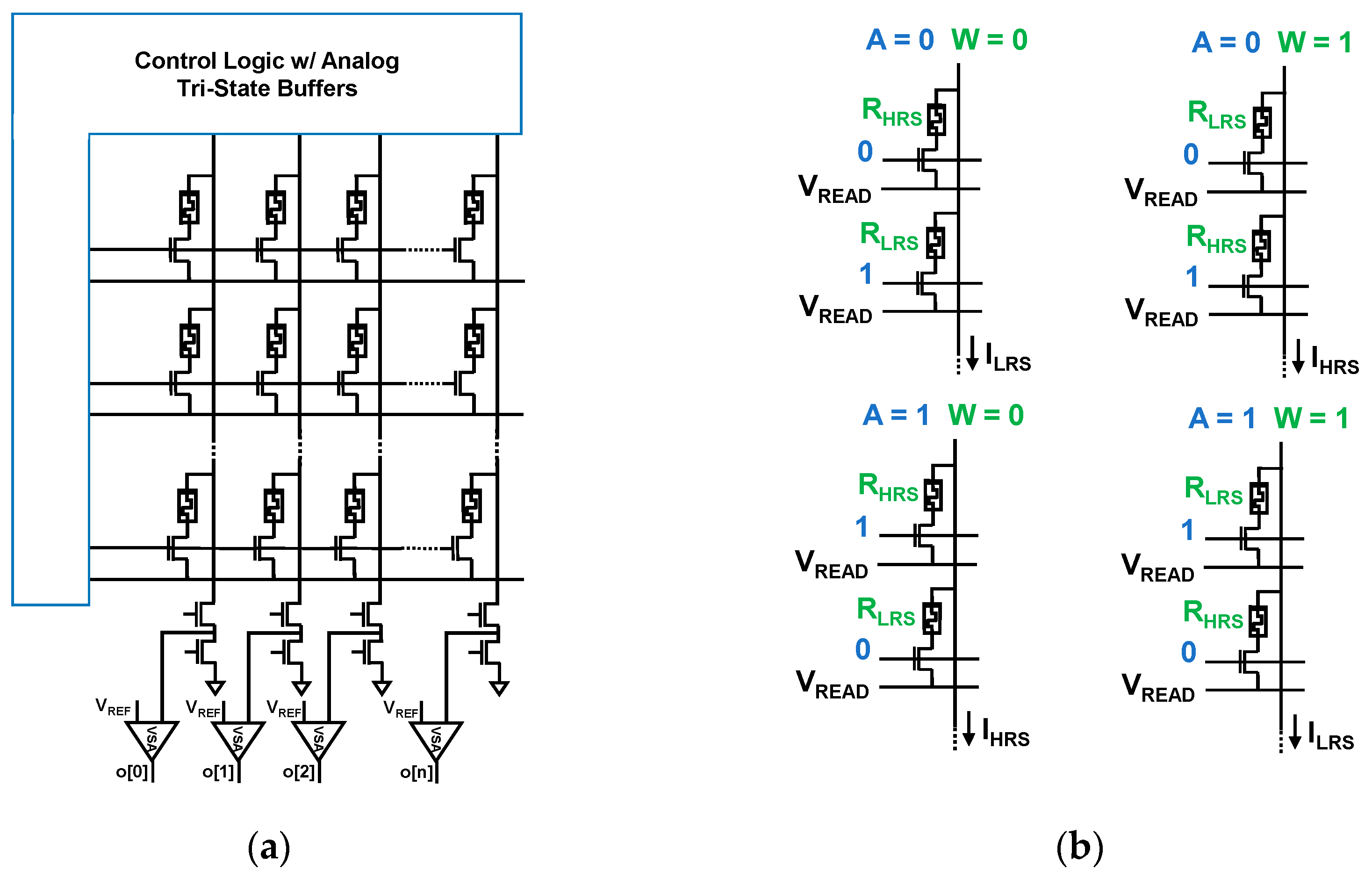
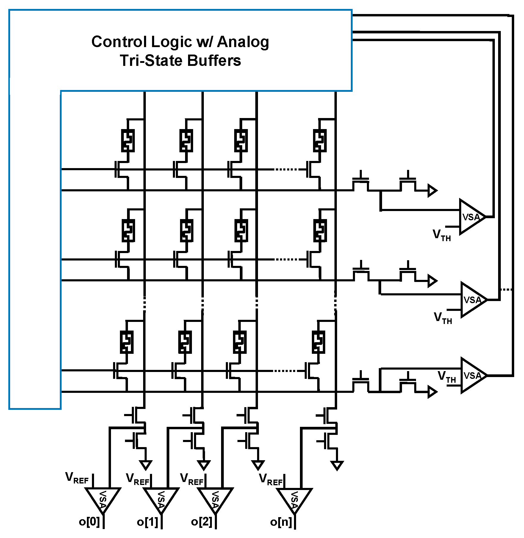
2.2.2. Binarized Neural Networks with Analog Vector Matrix Multiplication

The computation in the analog domain of the vector matrix multiplication with resistive memory devices has been shown to be a promising solution for accelerating in hardware the execution of deep neural networks. In this framework, the weights of the neural network are mapped into the analog non-volatile resistance of RRAM devices of a crossbar array [3], while the input activations to a neuron are mapped to voltage pulses with amplitude or duration proportional to the input value. By applying such input activations to the rows of the crossbar and by providing a virtual ground to the end of each crossbar column, the current flowing in each crossbar column is linearly proportional to the result of the vector matrix multiplication, that is computed in a single step thanks to Ohm’s and Kirchhoff’s current laws. However, such architecture presents some challenges due to resistive memory devices non-idealities such as the resistive state variability, which limits the number of bits that can be reliably encoded into a single RRAM device. Furthermore, providing a virtual ground at each crossbar column comes at the expense of a large chip area occupied by the peripheral circuitry due to the need of operational amplifiers [33] and analog to digital converters (ADCs) which limit the area efficiency especially when many rows are read in parallel. Thus, the need for the virtual ground becomes the main bottleneck for such architecture, introducing a tradeoff between crossbar density and latency (i.e., the same operational amplifier and ADC pair can be shared among multiple crossbar columns; however, reducing the maximum throughput). A more robust solution to RRAM variability, which is also more efficient in terms of chip area occupancy, are BNNs. In fact, binary weights can be reliably stored in a crossbar array using a pair of RRAM devices in the same column, as shown in Figure 6b. To store a +1 weight, the two RRAM devices are programmed into an LRS/HRS configuration, while to store a −1 the opposite configuration is used (see Figure 6b). When computing the binary vector matrix multiplication, which is equivalent to the combined bitwise XNOR and popcount operations, the two FETs in series with the RRAMs representing a single weight are driven with complementary signals that encode the +1/-1 input activations so that only one FET is active at time. As a result, the current flowing through each crossbar column is proportional to the sum of all the positive results of the products between the input activations and each neuron’s weights. Using this approach, the operational amplifier and ADC can be replaced by a much more compact voltage sense amplifiers (VSAs) circuit [21,22], implementing the architecture shown in Figure 6a, thus reducing the required chip area and improving the throughput and the energy efficiency. Instead of voltage sensing, the same approach could also be implemented by using current mode sense amplifiers [34], however resulting in lower energy efficiency [35]. Nevertheless, when using a sense amplifier, no virtual ground is available at the end of the crossbar columns. Thus, a FET implementing a pull-up or pull-down resistor must be used, thereby realizing a voltage divider between the equivalent parallel resistance of the active 1T1R devices in a column and the pull-up or pull-down resistor. Due to the use of a voltage divider, the linear relation between the number of active devices and the input to the VSA is lost. Nevertheless, He et al. [21] showed that the method is robust and that the output activation can be reliably determined by comparing the voltage from the voltage divider with an appropriate threshold using the VSA, retaining high inference accuracy also when process variations are considered. However, the number of devices that can be reliably read in parallel to compute the MAC operation is limited and strictly dependent on RHRS, RLRS, the pull-down resistance (RPD) and the VSA threshold voltage. As shown in Figure 7a, considering the case with 15 devices read in parallel during each MAC, increasing RPD changes the required VSA threshold voltage. Ideally, a linear relation between VN and the number of positive products is desirable. However, to achieve such linearity very low RPD values should be used, resulting in a considerable reduction of the dynamic range at the input of the comparator thus increasing the probability of errors due to the effect of resistive state variability. On the other hand, a too high RPD value causes the input voltage (i.e., VN) to the VSA to rapidly saturate to VREAD. While, considering a fixed VTH and lowering RPD increases the number of devices that can be read in parallel during each MAC operation, as shown in Figure 7b. However, too low RPD values would require large FET devices and the effect of line parasitic resistances may affect the circuit reliability making the circuit more susceptible to noise. Thus, in this framework, MAC operations are split into multiple computing steps using the input split method [21,36], so that partial MAC operations are computed using the maximum parallelism enabled by the designed architecture. These partial results need to be accumulated and the result of the accumulation is compared to a trained threshold to produce the neuron output activation.
Compared to the SIMPLY implementation of the BNN MAC operation, this approach is considerably faster, as it requires fewer computing steps, and more energy efficient since no RRAM device is switched during computations. However efficient, this approach is specialized for BNNs and do not provide the reconfigurability of the kind of operations computed in-memory enabled by SIMPLY. Thus, the crossbar array can only be used for BNN inferencing and storage applications.

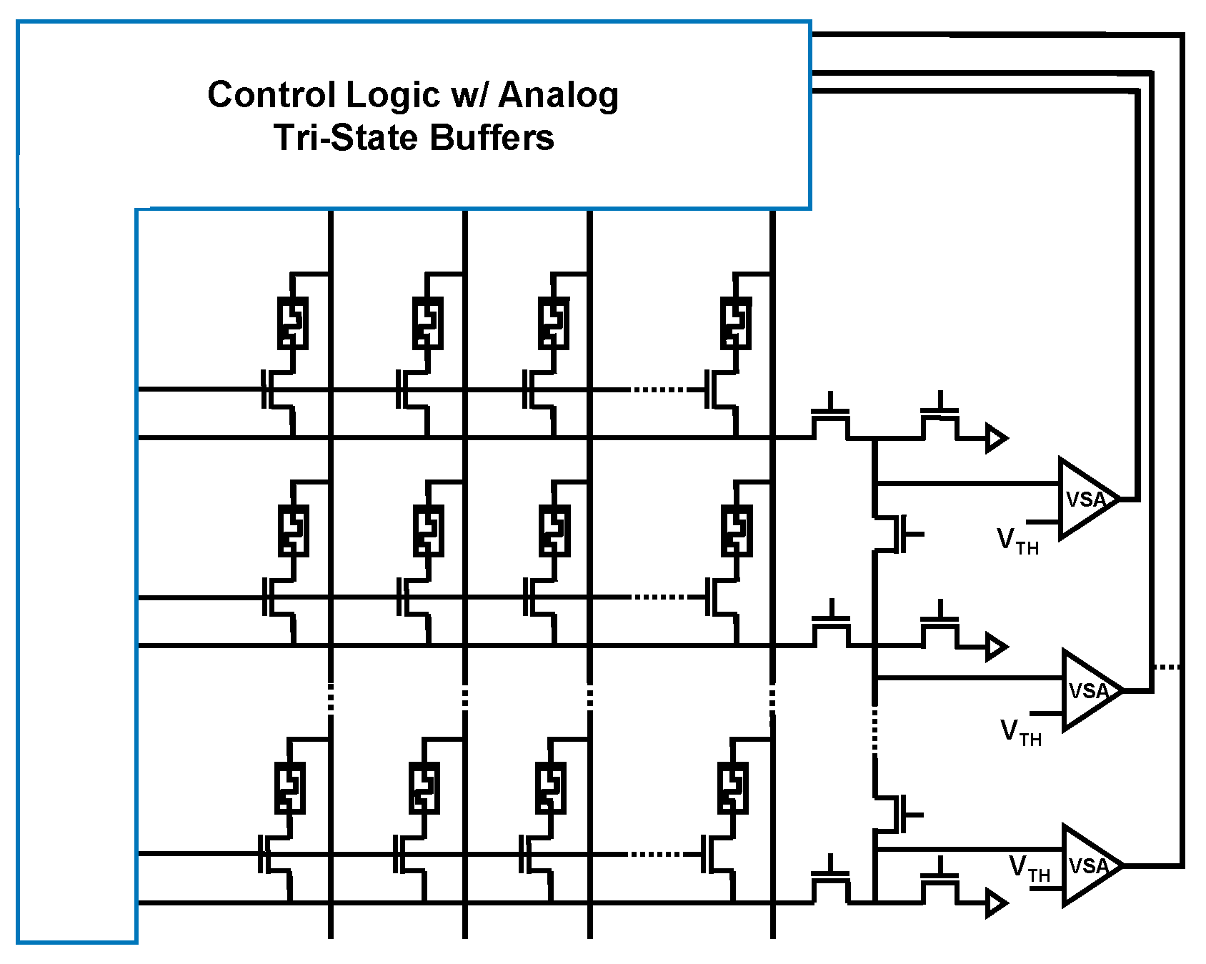
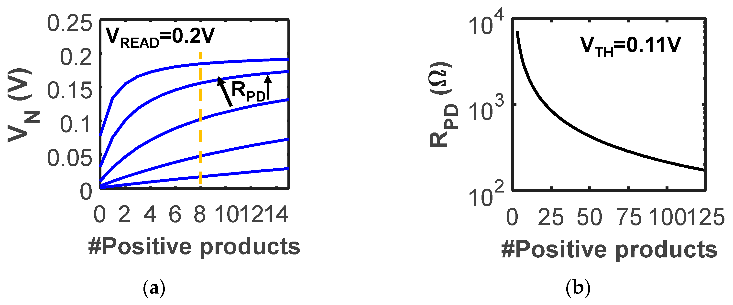
2.3. Merging SIMPLY and BNN Analog Vector Matrix Multiplication Accelerator

As discussed in the previous sections, both the SIMPLY computing paradigm and the BNN analog vector matrix multiplication (AVMM) accelerator are promising solution for IoT and edge computing devices and applications, as they provide considerable energy savings when computing different kinds of operations. While using multiple crossbar arrays specialized for different applications would be a solution to implement both computing paradigms on the same chip, it would result in an inefficient exploitation of the already scarce resources available to low-power devices. A better solution would be introducing the possibility to reconfigure the available resources to implement both computing paradigms on the same crossbar, provided that the additional flexibility must not determine the need for a much more complex, large, and inefficient peripheral circuitry. As it can be noted from Figure 4 and Figure 6a, the circuit architecture used to implement both computing paradigms are indeed similar, relying on some FET devices used to implement RG in the SIMPLY paradigm and RPD in the BNN AVMM acceleration, VSAs and corresponding voltage thresholds. However, when considering the same 1T1R crossbar array, there are some differences between the two architectures and in their respective control signals management. Specifically, when performing a read step in the SIMPLY computing paradigm the select line corresponding to the row where the devices are located is activated, the read voltages are applied to the crossbar columns and the output is read from the appropriate crossbar row by means of the VSA and of a threshold. This holds true both when performing an IMPLY between devices located in the same row and when the devices are located in the same column.
On the other hand, to execute a MAC operation in the analog BNN AVMM accelerator the select lines encode the neurons input activations, and each select line must be shared among the neuron in the same neural network layer. Thus, read voltages need to be applied to the crossbar rows while the voltages encoding the result of the MAC operations are read out from the crossbar columns using VSAs with appropriate thresholds.
Therefore, to merge the two approaches the peripheral circuitry comprising the VSAs and pull-down resistance needs to be repeated both at the columns and the rows of the crossbar with limited additional complexity, resulting in the architecture shown in Figure 8. While the need of additional VSAs increases the chip area, it enables the coexistence of the two in-memory computing paradigms on the same crossbar. In addition, it improves the SIMPLY architecture by increasing achievable parallelism when performing operations on devices on the same columns but different rows, thus accelerating the copy of data between the rows of the crossbar array. In fact, only one IMPLY operation between devices on the same column using the SIMPLY architecture in Figure 4 can be executed in one computing step due to the lack of SA at the crossbar columns. Instead, the addition of SAs at each crossbar column enables the parallel execution of IMPLY operation on multiple columns, by applying VREAD to the crossbar rows and comparing the VN voltage with the appropriate threshold at each column. Since IMPLY operations can be performed both on devices on the same row or column by applying VREAD at the crossbar columns and rows, respectively, the selector transistor in series with each RRAM device is subject to different source-bulk voltages. Nevertheless, since VREAD is small, the influence of the body effect can be minimized by driving these transistors with sufficiently high gate voltages. Also, using the same VSA threshold voltage for the two computing paradigms translates to different optimal RG and RPD values, requiring appropriate control of the gate voltage of the FET devices implementing such resistances. In fact, RPD is much lower than RG since more devices are read in parallel compared to SIMPLY. A too high RPD would let the input of the VSA saturate at VREAD with only a few active devices in LRS, thus hindering the correct circuit operation.
A specific advantage of the proposed architecture is the possibility to exploit both the SIMPLY and BNN AVMM computing paradigms on the same crossbar array, which is particularly useful for some applications. For instance, when implementing a complete BNN exploiting the AVMM in-memory acceleration the MAC operations are computed in multiple steps, using the input split strategy [21]. Thus, the computation of logic operations is required to determine each neuron output activation, and consist in the accumulation of the intermediate MAC results and a comparison with a trained threshold. While as discussed in Section 2.2.1 the cost for performing accumulations with SIMPLY rapidly increases with the number of bits to be added, the use of the BNN AVMM for computing intermediate MAC results drastically reduces the number of bits that needs to be accumulated with SIMPLY. Thus, while intermediate computations could also be executed on task-specific CMOS digital circuits, merging the two computing approaches enables achieving high performance by exploiting the intrinsic high degree of parallelism in the computation, without requiring additional circuits complexity. Also, this approach is particularly advantageous for large neural network implementations that require storing the network parameters over multiple chips thus incurring in the inter-chip communication penalty that can exceed the RRAM programming time and energy. Overall, the proposed architecture is an extremely flexible solution for ultra low-power applications.

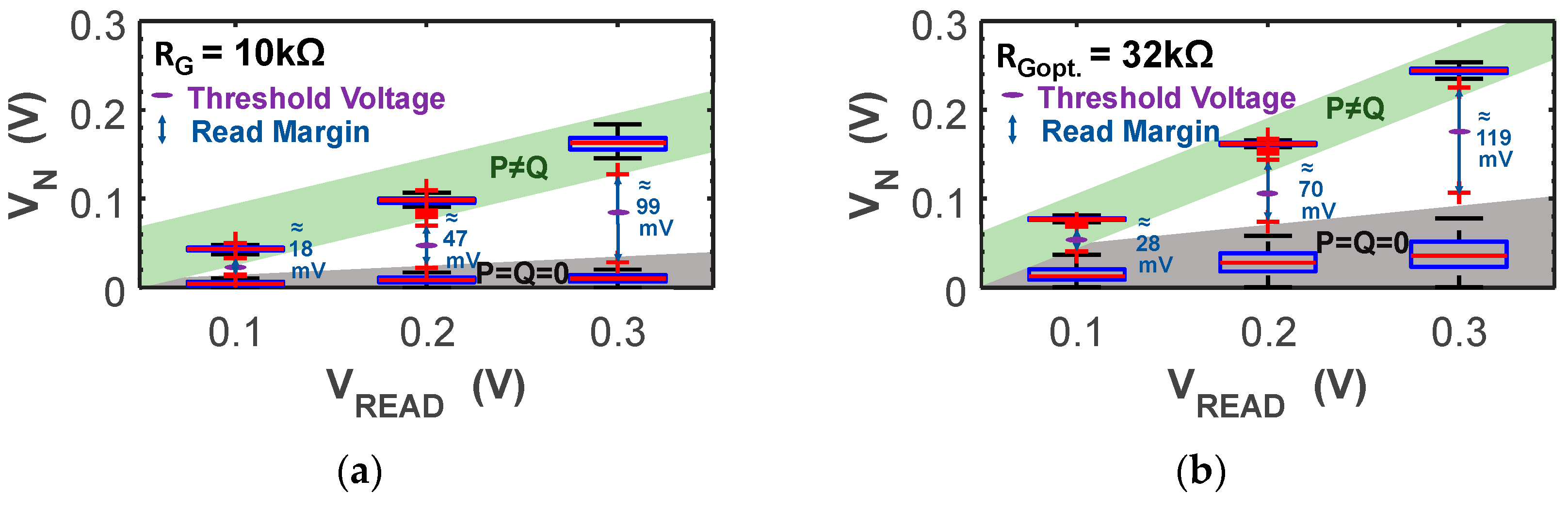
2.4. Circuit Design Tradeoffs for Performance and Reliability

The circuit design of the proposed architecture is directly connected to the specific requirements of possible use case applications [3,10], which may require the use of different resistive memory technologies to meet specific requirements. Thus, the correct selection of the most appropriate resistive memory technology becomes very important and is governed by the existing design tradeoffs that are aimed at providing low operation energy, fast speed, high integration density, and high reliability, as discussed in this section.
Specifically, to minimize the energy consumption different approaches are possible. The most effective solution is to employ resistive memory technologies with low current compliance (IC), and therefore higher RLRS. Firstly, the use of lower IC leads to lower energy dissipation when programming a device, thus tackling the main energy limitation associated to the SIMPLY paradigm, largely improving the energy efficiency. Secondly, higher RLRS values also lower the energy required for each parallel read both when computing an IMPLY in the SIMPLY paradigm and when implementing the BNN AVMM. Furthermore, this strategy results in additional advantages on the overall area consumption and speed. By lowering IC, the required size of the FET devices used as selector devices and in the array periphery is reduced, thus reducing the chip area. Also, using higher RLRS increases the parallelism of the BNN AVMM implementation, since more rows can be read in parallel when using the same RPD resistance. However, cycle-to-cycle (C2C) and device-to-device (D2D) variability is inversely proportional to IC [31,37], thus too low IC values may affect the circuit reliability depending on the memory technology employed. The energy efficiency is also improved by reducing VREAD, which in turns reduces the energy consumption during the read operations performed both in the SIMPLY and in the BNN AVMM computing paradigms. Also, in this case the reliability issue may arise, since too low read voltages would reduce the RM and the SNR at the input of the VSAs.
Limiting the overall chip area is indeed very important to reduce the fabrication costs. Thus, higher crossbar array densities are beneficial. To this end, two main technology features are prominently relevant, namely the memory cell feature size and the possibility to implement dense 3D structures. While the use of a selector transistor effectively solves the sneak-path problem, it increases the chip area, due to the larger feature size of the 1T1R device (i.e., 8F2) with respect to a passive 1R device [38] (i.e., 4F2), and requires a higher number of control signals and interconnections. Other passive selector devices could introduce the required high non-linearity to solve the sneak-path issue while retaining the 4F2 [39] device feature size and could be also used with the proposed architecture by changing the driving voltage scheme. Also, the equivalent number of memory devices per chip area can be increased by fabricating 3D array structures. These can be implemented by stacking horizontal crossbars arrays, and even more efficiently by realizing a 3D vertical structure that would lead to the highest densities and costs reduction [40].
Also, crossbar line parasitic effects, such as line resistance and coupling capacitance, influence the maximum attainable computing speed. In fact, these effects together with the resistance of RRAM devices introduce propagation delays that grow as the size of the crossbar arrays is increased [41], therefore introducing a tradeoff between computing speed and maximum array size.
Finally, to ensure high circuit reliability, in addition to providing a sufficient RM at the input of the VSA, memory technologies with high endurance and retention should be preferred. In particular, endurance is a key parameter for the SIMPLY paradigm. In fact, while the analog BNN VMM only requires reading the state of RRAM devices, the SIMPLY principle of operations relies on the conditional programming of RRAM devices to perform computation. Long retention, on the other hand, is required to prevent periodic memory refresh cycles that would degrade the architecture’s efficiency.

3. Discussion

While SIMPLY was shown in previous works to be an effective solution for the in-memory computation of logic operations (e.g., XNOR [19], full adders [31]), its effectiveness for the computation of the set of logic operations required to implement a BNN inference task was limited due to the large number of computing steps required to implement the multiply and accumulate (MAC) operation. In fact, as previously mentioned, the number of computing steps needed for a MAC operation grows exponentially with the number of inputs to a BNN layer [19] making SIMPLY suitable only for smaller networks. As shown in Table 1, the energy reduction (i.e., ≈400 times lower) with respect to a conventional embedded system implementation reported in a previous work [19] is much larger than the latency improvement (i.e., ≈26 times lower), which would further reduce as the network size increases. By enabling the coexistence on the same crossbar array of both the SIMPLY and AVMM computing paradigms at the cost of a limited complexity increase, the proposed in-memory computing architecture achieves substantial performance improvements when considering a BNN inference task, while retaining the hardware reconfigurability feature that is required by edge computing devices and applications. This is clearly reported in Table 1, where we show, considering the ideal case both for SIMPLY and the proposed architectures where all the network parameters and computing devices are stored in a single crossbar, that also in the worst-case the proposed architecture drastically reduces the latency and energy consumption compared to the SIMPLY architecture when computing the same inference task, achieving an energy delay product (EDP) improvement larger than 103.
As discussed in Section 2.4, the performance, reliability, and target application for the proposed computing architecture strongly depend on the resistive memory technology employed. While the device endurance does not impact on the AVMM implementation, it is a very important discriminant for SIMPLY. Applications performing intensive computations require very high endurance (i.e., >1014). Thus, for this application spin-transfer torque magnetic RAM (STT-MRAM) devices are more suitable candidate, thanks to their high retention (>10 years), endurance (>1014) and switching speed (~ns) [43]. However, STT-MRAM devices have usually small tunnel magneto resistance (TMR) which leads to a very small memory window that can affect the circuit reliability if not address properly, especially when implementing the AVMM. For instance, Gao et al. [44] showed that STT-MRAM can indeed be used to accelerate the AVMM for BNNs, however at the cost of additional in-hardware calibration steps and more complex peripheral circuitry, which include operational amplifiers to implement the virtual ground, thus limiting the throughput, energy efficiency, and chip density. Conversely, devices characterized by lower endurance are better suited for applications requiring less frequent burst operations, such as smart sensors. For instance, to provide a reliable device operation over a 10-year period with a memory technology providing a 108 endurance would limit the computing speed to 20 inferences per minute without introducing mitigation strategies, such as periodically changing devices used for computations. Currently, several emerging non-volatile memory (NVM) technologies were shown to achieve endurance >108. Among these technologies, phase change memory (PCM) devices are the most mature and offer long retention, high endurance (>1012) [45,46,47], but require higher switching currents compared to other ENVMs, therefore limiting the integration density. Also, ferroelectric tunnel junction (FTJ) devices are a promising candidate for the development of ultra-low-power in-memory computing architectures thanks to low programming energy and fast speed. However, high endurance, retention, and scalability still need to be fully demonstrated [45,47]. At the state of the art, RRAM technologies provide the best overall characteristics. Depending on the used stack of materials, RRAMs can achieve endurance up to 1010 [48], long retention, large memory window (≈10), and can be used to realize vertical 3D structures similar to flash memory technology, leading to ultra-dense arrays. However, two main technology-related challenges remain to be solved. Specifically, C2C and D2D variability lead to random resistance distributions which spread when lowering IC [31,37] thus introducing a tradeoff between energy efficiency, reliability, and throughput when performing the AVMM. Also, to achieve ultra-dense vertical 3D arrays while preventing the sneak path issue, a particular research focus must be directed to the development of compatible selector devices with a strongly non-linear conduction behavior [39,49].

4. Materials and Methods

4.1. Circuit Simulations

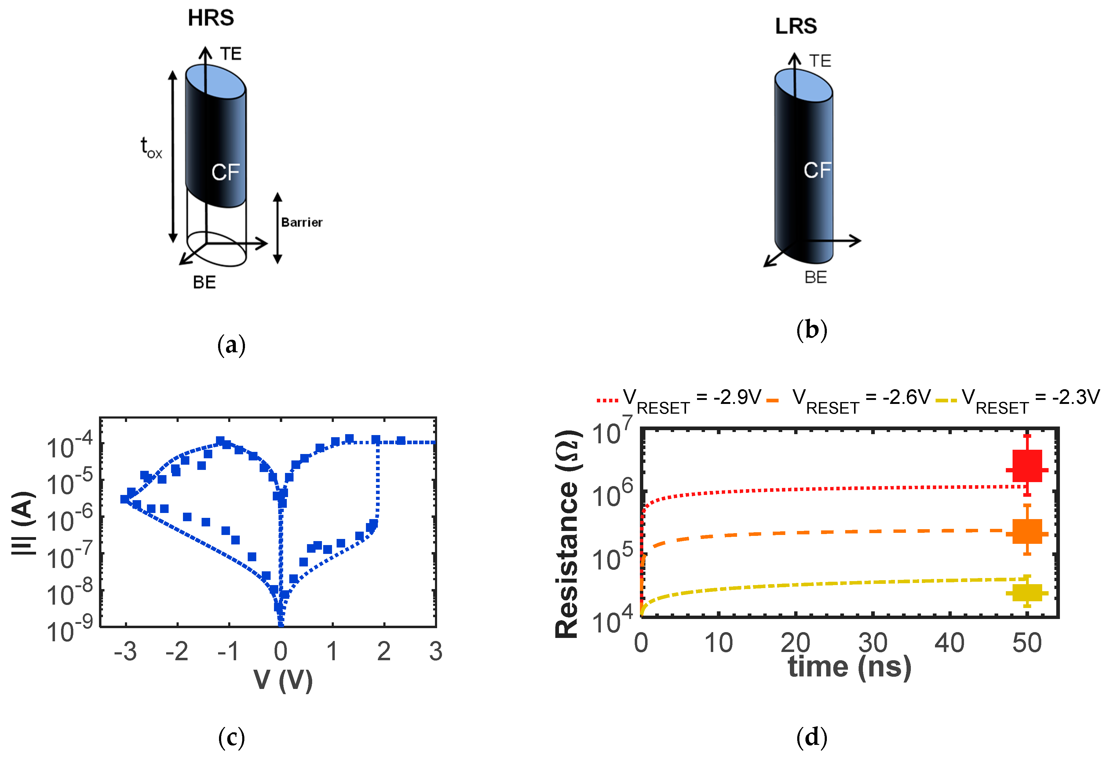
4.1.1. RRAM Physics-Based Compact Model

The performance of the proposed architecture was estimated by means of circuit simulation performed on Cadence Virtuoso® software, using the RRAM physics-based compact model from [50] available on nanoHub, that was calibrated on a TiN/HfOx/AlOx/Pt RRAM technology from [26] that is programmed with an IC of 100 µA. A sketch of the compact model is reported in Figure 9a,b. While other general-purpose memristors [51,52,53,54] and physics-based RRAM compact models [55,56,57,58,59,60] exist in the literature, the used RRAM physics-based compact model is particularly suited for estimating the circuit performance and reliability, as it includes all the relevant RRAM devices’ characteristics and non-idealities (e.g., dynamic temperature modelling, resistive state variability, and RTN) which only a few other physics-based compact models [56,57] consider, as discussed in [28]. Specifically, the compact model approximates the device resistance as the sum of a conductive filament (CF) and a dielectric barrier component (see Figure 9a,b). Differential equations model the field-activated and temperature-accelerated bond breaking during set, and the field-driven oxygen ions’ drift and recombination during reset, thus reproducing the dielectric barrier thickness dynamics. Thermal effects are also modeled with differential equation, leading to accurate results also when ultra-fast pulses are considered. As shown in Figure 9c,d, the compact model well reproduces with a single set of parameters both the DC IV and the response to fast reset pulses. Additionally, the compact model includes all the RRAM non-idealities that are relevant to accurately estimate circuit performance and reliability, specifically RTN and variability [28,50]. The complete list of calibrated parameters is available in [20].

4.1.2. SIMPLY Simulations

The performance of the proposed architecture when operating as SIMPLY were estimated considering 1ns read and write pulses which result in a 4 ns execution time of a single IMPLY or FALSE operation. The RG resistors were simulated using planar NMOS devices in a 45 nm technology [30] with a channel width of 250 nm and a channel length of 50 nm. Also, the energy contribution of the SA is considered by simulating the circuit shown in Figure 4 in the same 45 nm technology, which results in an average energy consumption of 8 fJ when operated with a 2 V VDD over a temperature range from 0 °C to 85 °C, as reported in [20]. The device SET and RESET operations are achieved using 1 ns voltage pulses with amplitudes 3 V and –2.9 V, respectively. The SET and RESET amplitudes were determined using the physics-based compact model to ensure that a memory window larger than 10 is achieved also for very short voltage pulses, as discussed in [19]. The read margin (RM) and performance for both IMPLY and FALSE operations reported in Table 2 and Table 3 were estimated including the effect of variability and RTN during the read operation by repeating the simulations (i.e., 50 trials) and reseeding the random sources. Additional information regarding SIMPLY circuit simulations and the list of variability and RTN model parameters are available in [20,50], respectively.

4.2. Implemented Neural Network

To benchmark the performance of the proposed architecture against the SIMPLY implementation, the same BNN from [19,42] was implemented. The network consists of a single hidden layer with 1000 neurons, and classify the digits 0−9 from the MNIST handwritten digits dataset [61]. The 20 × 20 pixels images are binarized to black and white images before training. The training was performed on 9500 images using the DoReFa-Net algorithm [32] considering one bit for weights and activations and 32 bits for the gradients. 2500 and 2000 images were used for validation and testing, respectively. The trained network achieves an accuracy of 91.4% [19].

4.3. BNN Performance Estimates

The trained network parameters were mapped to RRAM devices’ resistance values including the effect of resistive state variability. The performance of the proposed architecture was estimated on an inference task by means of circuit simulation, where the AVMM is used to compute intermediate results of the MAC operations while SIMPLY is used to accumulate intermediate results and to compute each layer output activations. Intermediate MAC operations are needed to preserve the same NMOS size for implementing both RPD and RG by just adjusting VGS (i.e., VGS is 1.48 V and 2.9 V when operating the crossbar array as SIMPLY or BNN AVMM accelerator, respectively). With the considered RRAM technology, a maximum of 15 crossbar rows can be reliably read in parallel during the AVMM. Thus, as an example, 27 (i.e., 400/15) computing steps are needed to compute all the intermediate MAC operations in the first layer. After each parallel read operation, the intermediate MAC results are stored in RRAM devices in the crossbar array and accumulated using the SIMPLY accumulator implementation shown in Figure 5e [20]. The results of the accumulations are compared with a threshold to produce each layer output activations using the SIMPLY comparator implementation from [19], which requires 9 m + m ( m + 1 ) 2 where m is the number of compared bits. Finally, the output layer computes the predicted class using the hardmax SIMPLY implementation reported in [19] which accounts for 1457 computing steps on the proposed architecture and determines the predicted class as the class with the highest activation value. Thus, a total of 7902 computing steps are required for each inference, resulting in a 31.6 µs inference latency when 1 ns voltage pulses are used, as reported in Table 1. The worst-case energy for an inference task reported in Table 1 is estimated by running the neural network on the complete test set and considering only the worst-case energy for each IMPLY, SET, and FALSE operations for each specific input combination. The VSA energy contribution is included when performing both SIMPLY and BNN MAC operations. By considering the worst-case energy for each SIMPLY operation, which is the main contribution to the overall energy consumption, the energy assessments are indeed slightly overestimated, and roughly account for additional energy contributions possibly introduced by the peripheral circuitry. Nevertheless, even when increasing by 20% the energy consumption to account for the decoders and drivers considering the power breakdown reported by He at al. [21], the results (see Table 1) underline the remarkable energy efficiency in comparison with conventional embedded system implementations.

5. Conclusions

In this work, we proposed a novel in-memory computing architecture that enables the coexistence on the same crossbar array of the SIMPLY logic-in-memory computing approach and of the BNN AVMM. Design tradeoffs and requirements for circuit performance and reliability were analyzed in depth. The performance of the proposed architecture on an inference task were benchmarked against a pure SIMPLY implementation by means of circuit simulations enabled by a calibrated RRAM physics-based compact model. The results show that the proposed approach drastically improves the EDP by a factor >103, indicating that the proposed architecture is a viable solution for the realization of reconfigurable ultra-low-power hardware accelerators for edge computing applications.

Author Contributions

Conceptualization, T.Z. and F.M.P.; methodology, T.Z.; software, T.Z., F.M.P. and P.P.; validation, T.Z.; writing—original draft preparation, T.Z.; writing—review and editing, T.Z., F.M.P. and P.P.; supervision, F.M.P. and P.P. All authors have read and agreed to the published version of the manuscript.

Funding

This research received no external funding.

Data Availability Statement

The data presented in this study are available within the article.

Conflicts of Interest

The authors declare no conflict of interests.

References

  1. Zhang, W.; Gao, B.; Tang, J.; Yao, P.; Yu, S.; Chang, M.-F.; Yoo, H.-J.; Qian, H.; Wu, H. Neuro-Inspired Computing Chips. Nat. Electron. 2020, 3, 371–382. [Google Scholar] [CrossRef]
  2. Deng, S.; Zhao, H.; Fang, W.; Yin, J.; Dustdar, S.; Zomaya, A.Y. Edge Intelligence: The Confluence of Edge Computing and Artificial Intelligence. IEEE Internet Things J. 2020, 7, 7457–7469. [Google Scholar] [CrossRef] [Green Version]
  3. Pedretti, G.; Ielmini, D. In-Memory Computing with Resistive Memory Circuits: Status and Outlook. Electronics 2021, 10, 1063. [Google Scholar] [CrossRef]
  4. Kvatinsky, S.; Belousov, D.; Liman, S.; Satat, G.; Wald, N.; Friedman, E.G.; Kolodny, A.; Weiser, U.C. MAGIC—Memristor-Aided Logic. IEEE Trans. Circuits Syst. II: Express Briefs 2014, 61, 895–899. [Google Scholar] [CrossRef]
  5. Ziegler, T.; Waser, R.; Wouters, D.J.; Menzel, S. In-Memory Binary Vector–Matrix Multiplication Based on Complementary Resistive Switches. Adv. Intell. Syst. 2020, 2, 2000134. [Google Scholar] [CrossRef]
  6. Kingra, S.K.; Parmar, V.; Chang, C.-C.; Hudec, B.; Hou, T.-H.; Suri, M. SLIM: Simultaneous Logic-in-Memory Computing Exploiting Bilayer Analog OxRAM Devices. Sci. Rep. 2020, 10. [Google Scholar] [CrossRef] [Green Version]
  7. Pei, J.; Deng, L.; Song, S.; Zhao, M.; Zhang, Y.; Wu, S.; Wang, G.; Zou, Z.; Wu, Z.; He, W.; et al. Towards Artificial General Intelligence with Hybrid Tianjic Chip Architecture. Nature 2019, 572, 106–111. [Google Scholar] [CrossRef] [PubMed]
  8. Xiao, T.P.; Bennett, C.H.; Feinberg, B.; Agarwal, S.; Marinella, M.J. Analog Architectures for Neural Network Acceleration Based on Non-Volatile Memory. Appl. Phys. Rev. 2020, 7, 031301. [Google Scholar] [CrossRef]
  9. Saxena, V. Neuromorphic Computing: From Devices to Integrated Circuits. J. Vac. Sci. Technol. B 2021, 39, 010801. [Google Scholar] [CrossRef]
  10. Berggren, K.; Xia, Q.; Likharev, K.K.; Strukov, D.B.; Jiang, H.; Mikolajick, T.; Querlioz, D.; Salinga, M.; Erickson, J.R.; Pi, S.; et al. Roadmap on Emerging Hardware and Technology for Machine Learning. Nanotechnology 2020, 32, 012002. [Google Scholar] [CrossRef]
  11. Benoit, P.; Dalmasso, L.; Patrigeon, G.; Gil, T.; Bruguier, F.; Torres, L. Edge-Computing Perspectives with Reconfigurable Hardware. In Proceedings of the 2019 14th International Symposium on Reconfigurable Communication-centric Systems-on-Chip (ReCoSoC); York, UK, 1–3 July 2019; pp. 51–58. [Google Scholar]
  12. Yu, J.; Du Nguyen, H.A.; Abu Lebdeh, M.; Taouil, M.; Hamdioui, S. Enhanced Scouting Logic: A Robust Memristive Logic Design Scheme. In Proceedings of the 2019 IEEE/ACM International Symposium on Nanoscale Architectures (NANOARCH), Qingdao, China, 17−19 July 2019; pp. 1–6. [Google Scholar]
  13. Borghetti, J.; Snider, G.S.; Kuekes, P.J.; Yang, J.J.; Stewart, D.R.; Williams, R.S. ‘Memristive’ Switches Enable ‘Stateful’ Logic Operations via Material Implication. Nature 2010, 464, 873–876. [Google Scholar] [CrossRef]
  14. Siemon, A.; Menzel, S.; Waser, R.; Linn, E. A Complementary Resistive Switch-Based Crossbar Array Adder. IEEE J. Emerg. Sel. Top. Circuits Syst. 2015, 5, 64–74. [Google Scholar] [CrossRef] [Green Version]
  15. Siemon, A.; Drabinski, R.; Schultis, M.J.; Hu, X.; Linn, E.; Heittmann, A.; Waser, R.; Querlioz, D.; Menzel, S.; Friedman, J.S. Stateful Three-Input Logic with Memristive Switches. Sci. Rep. 2019, 9, 1–13. [Google Scholar] [CrossRef] [PubMed] [Green Version]
  16. Hu, S.-Y.; Li, Y.; Cheng, L.; Wang, Z.-R.; Chang, T.-C.; Sze, S.M.; Miao, X. Reconfigurable Boolean Logic in Memristive Crossbar: The Principle and Implementation. IEEE Electron Device Lett. 2019, 40, 200–203. [Google Scholar] [CrossRef]
  17. Puglisi, F.M.; Zanotti, T.; Pavan, P. SIMPLY: Design of a RRAM-Based Smart Logic-in-Memory Architecture Using RRAM Compact Model. In Proceedings of the ESSDERC 2019—49th European Solid-State Device Research Conference (ESSDERC), Krakow, Poland, 23−26 September 2019; pp. 130–133. [Google Scholar]
  18. Courbariaux, M.; Hubara, I.; Soudry, D.; El-Yaniv, R.; Bengio, Y. Binarized Neural Networks: Training Deep Neural Networks with Weights and Activations Constrained To+ 1 or-1. arXiv 2016, arXiv:1602.02830. [Google Scholar]
  19. Zanotti, T.; Puglisi, F.M.; Pavan, P. Reliability and Performance Analysis of Logic-in-Memory Based Binarized Neural Networks. IEEE Trans. Device Mater. Reliab. 2021, 1. [Google Scholar] [CrossRef]
  20. Zanotti, T.; Puglisi, F.M.; Pavan, P. Reconfigurable Smart In-Memory Computing Platform Supporting Logic and Binarized Neural Networks for Low-Power Edge Devices. IEEE J. Emerg. Sel. Top. Circuits Syst. 2020, 1. [Google Scholar] [CrossRef]
  21. He, W.; Yin, S.; Kim, Y.; Sun, X.; Kim, J.-J.; Yu, S.; Seo, J.-S. 2-Bit-Per-Cell RRAM-Based In-Memory Computing for Area-/Energy-Efficient Deep Learning. IEEE Solid State Circuits Lett. 2020, 3, 194–197. [Google Scholar] [CrossRef]
  22. Sun, X.; Peng, X.; Chen, P.; Liu, R.; Seo, J.; Yu, S. Fully Parallel RRAM Synaptic Array for Implementing Binary Neural Network with (+1, −1) Weights and (+1, 0) Neurons. In Proceedings of the 2018 23rd Asia and South Pacific Design Automation Conference (ASP-DAC), Jeju, Korea, 22−25 January 2018; pp. 574–579. [Google Scholar]
  23. Vieira, J.; Giacomin, E.; Qureshi, Y.; Zapater, M.; Tang, X.; Kvatinsky, S.; Atienza, D.; Gaillardon, P.-E. A Product Engine for Energy-Efficient Execution of Binary Neural Networks Using Resistive Memories. In Proceedings of the 2019 IFIP/IEEE 27th International Conference on Very Large Scale Integration (VLSI-SoC), Cuzco, Peru, 6−9 October 2019; pp. 160–165. [Google Scholar]
  24. Yi, W.; Kim, Y.; Kim, J.-J. Effect of Device Variation on Mapping Binary Neural Network to Memristor Crossbar Array. In Proceedings of the 2019 Design, Automation Test in Europe Conference Exhibition (DATE), Florence, Italy, 25−29 March 2019; pp. 320–323. [Google Scholar]
  25. Qin, Y.-F.; Kuang, R.; Huang, X.-D.; Li, Y.; Chen, J.; Miao, X.-S. Design of High Robustness BNN Inference Accelerator Based on Binary Memristors. IEEE Trans. Electron Devices 2020, 67, 3435–3441. [Google Scholar] [CrossRef]
  26. Yu, S.; Wu, Y.; Chai, Y.; Provine, J.; Wong, H.-S.P. Characterization of Switching Parameters and Multilevel Capability in HfOx/AlOx Bi-Layer RRAM Devices. In Proceedings of the 2011 International Symposium on VLSI Technology, Systems and Applications, Hsinchu, Taiwan, 25−27 April 2011; pp. 1–2. [Google Scholar]
  27. Lehtonen, E.; Poikonen, J.H.; Laiho, M. Two Memristors Suffice to Compute All Boolean Functions. Electron. Lett. 2010, 46, 239–240. [Google Scholar] [CrossRef]
  28. Zanotti, T.; Puglisi, F.M.; Pavan, P. Reliability-Aware Design Strategies for Stateful Logic-in-Memory Architectures. IEEE Trans. Device Mater. Reliab. 2020, 20, 278–285. [Google Scholar] [CrossRef]
  29. Kvatinsky, S.; Satat, G.; Wald, N.; Friedman, E.G.; Kolodny, A.; Weiser, U.C. Memristor-Based Material Implication (IMPLY) Logic: Design Principles and Methodologies. IEEE Trans. Very Large Scale Integr. (VLSI) Syst. 2014, 22, 2054–2066. [Google Scholar] [CrossRef]
  30. Stine, J.E.; Castellanos, I.; Wood, M.; Henson, J.; Love, F.; Davis, W.R.; Franzon, P.D.; Bucher, M.; Basavarajaiah, S.; Oh, J.; et al. FreePDK: An Open-Source Variation-Aware Design Kit. In Proceedings of the 2007 IEEE International Conference on Microelectronic Systems Education (MSE’07), San Diego, CA, USA, 3−4 June 2007; pp. 173–174. [Google Scholar]
  31. Zanotti, T.; Zambelli, C.; Puglisi, F.M.; Milo, V.; Pérez, E.; Mahadevaiah, M.K.; Ossorio, O.G.; Wenger, C.; Pavan, P.; Olivo, P.; et al. Reliability of Logic-in-Memory Circuits in Resistive Memory Arrays. IEEE Trans. Electron Devices 2020, 67, 4611–4615. [Google Scholar] [CrossRef]
  32. Zhou, S.; Wu, Y.; Ni, Z.; Zhou, X.; Wen, H.; Zou, Y. DoReFa-Net: Training Low Bitwidth Convolutional Neural Networks with Low Bitwidth Gradients. arXiv 2018, arXiv:1606.06160. [Google Scholar]
  33. Krestinskaya, O.; Otaniyozov, O.; James, A.P. Binarized Neural Network with Stochastic Memristors. In Proceedings of the 2019 IEEE International Conference on Artificial Intelligence Circuits and Systems (AICAS), Hsinchu, Taiwan, 18−20 March 2019; pp. 274–275. [Google Scholar]
  34. Chen, W.-H.; Dou, C.; Li, K.-X.; Lin, W.-Y.; Li, P.-Y.; Huang, J.-H.; Wang, J.-H.; Wei, W.-C.; Xue, C.-X.; Chiu, Y.-C.; et al. CMOS-Integrated Memristive Non-Volatile Computing-in-Memory for AI Edge Processors. Nat. Electron 2019, 2, 420–428. [Google Scholar] [CrossRef]
  35. Wan, W.; Kubendran, R.; Gao, B.; Joshi, S.; Raina, P.; Wu, H.; Cauwenberghs, G.; Wong, H.S.P. A Voltage-Mode Sensing Scheme with Differential-Row Weight Mapping for Energy-Efficient RRAM-Based In-Memory Computing. In Proceedings of the 2020 IEEE Symposium on VLSI Technology, Honolulu, HI, USA, 16–19 June 2020; pp. 1–2. [Google Scholar]
  36. Yin, S.; Kim, Y.; Han, X.; Barnaby, H.; Yu, S.; Luo, Y.; He, W.; Sun, X.; Kim, J.-J.; Seo, J. Monolithically Integrated RRAM- and CMOS-Based In-Memory Computing Optimizations for Efficient Deep Learning. IEEE Micro. 2019, 39, 54–63. [Google Scholar] [CrossRef]
  37. Grossi, A.; Nowak, E.; Zambelli, C.; Pellissier, C.; Bernasconi, S.; Cibrario, G.; El Hajjam, K.; Crochemore, R.; Nodin, J.F.; Olivo, P.; et al. Fundamental Variability Limits of Filament-Based RRAM. In Proceedings of the 2016 IEEE International Electron Devices Meeting (IEDM), San Francisco, CA, USA, 3−7 December 2016. [Google Scholar]
  38. Mahmoodi, M.R.; Vincent, A.F.; Nili, H.; Strukov, D.B. Intrinsic Bounds for Computing Precision in Memristor-Based Vector-by-Matrix Multipliers. IEEE Trans. Nanotechnol. 2020, 19, 429–435. [Google Scholar] [CrossRef]
  39. Xia, Q.; Yang, J.J. Memristive Crossbar Arrays for Brain-Inspired Computing. Nat. Mater. 2019, 18, 309–323. [Google Scholar] [CrossRef]
  40. Yu, M.; Cai, Y.; Wang, Z.; Fang, Y.; Liu, Y.; Yu, Z.; Pan, Y.; Zhang, Z.; Tan, J.; Yang, X.; et al. Novel Vertical 3D Structure of TaOx-Based RRAM with Self-Localized Switching Region by Sidewall Electrode Oxidation. Sci. Rep. 2016, 6, 21020. [Google Scholar] [CrossRef] [Green Version]
  41. Fouda, M.E.; Eltawil, A.M.; Kurdahi, F. Modeling and Analysis of Passive Switching Crossbar Arrays. IEEE Trans. Circuits Syst. I: Regul. Pap. 2018, 65, 270–282. [Google Scholar] [CrossRef]
  42. McDanel, B.; Teerapittayanon, S.; Kung, H.T. Embedded Binarized Neural Networks. In Proceedings of the 2017 International Conference on Embedded Wireless Systems and Networks, Uppsala, Sweden, 20−22 February 2017; pp. 168–173. [Google Scholar]
  43. Kim, C.-H.; Lim, S.; Woo, S.Y.; Kang, W.-M.; Seo, Y.-T.; Lee, S.-T.; Lee, S.; Kwon, D.; Oh, S.; Noh, Y.; et al. Emerging Memory Technologies for Neuromorphic Computing. Nanotechnology 2019, 30, 032001. [Google Scholar] [CrossRef]
  44. Gao, S.; Chen, B.; Qu, Y.; Zhao, Y. MRAM Acceleration Core for Vector Matrix Multiplication and XNOR-Binarized Neural Network Inference. In Proceedings of the 2020 International Symposium on VLSI Technology, Systems and Applications (VLSI-TSA), Hsinchu, Taiwan, 10−13 August 2020; pp. 153–154. [Google Scholar]
  45. Slesazeck, S.; Mikolajick, T. Nanoscale Resistive Switching Memory Devices: A Review. Nanotechnology 2019, 30, 352003. [Google Scholar] [CrossRef] [PubMed]
  46. Ielmini, D.; Wong, H.-S.P. In-Memory Computing with Resistive Switching Devices. Nat. Electron. 2018, 1, 333–343. [Google Scholar] [CrossRef]
  47. Chen, A. A Review of Emerging Non-Volatile Memory (NVM) Technologies and Applications. Solid State Electron. 2016, 125, 25–38. [Google Scholar] [CrossRef]
  48. Nail, C.; Molas, G.; Blaise, P.; Piccolboni, G.; Sklenard, B.; Cagli, C.; Bernard, M.; Roule, A.; Azzaz, M.; Vianello, E.; et al. Understanding RRAM Endurance, Retention and Window Margin Trade-off Using Experimental Results and Simulations. In Proceedings of the 2016 IEEE International Electron Devices Meeting (IEDM), San Francisco, CA, USA, 3−7 December 2016. [Google Scholar]
  49. Shi, L.; Zheng, G.; Tian, B.; Dkhil, B.; Duan, C. Research Progress on Solutions to the Sneak Path Issue in Memristor Crossbar Arrays. Nanoscale Adv. 2020, 2, 1811–1827. [Google Scholar] [CrossRef]
  50. Puglisi, F.M.; Zanotti, T.; Pavan, P. Unimore Resistive Random Access Memory (RRAM) Verilog-A Model. nanoHUB 2019. [Google Scholar] [CrossRef]
  51. Yakopcic, C.; Taha, T.M.; Subramanyam, G.; Pino, R.E.; Rogers, S. A Memristor Device Model. IEEE Electron Device Lett. 2011, 32, 1436–1438. [Google Scholar] [CrossRef]
  52. Kvatinsky, S.; Friedman, E.G.; Kolodny, A.; Weiser, U.C. TEAM: ThrEshold Adaptive Memristor Model. IEEE Trans. Circuits Syst. I: Regul. Pap. 2013, 60, 211–221. [Google Scholar] [CrossRef]
  53. Kvatinsky, S.; Ramadan, M.; Friedman, E.G.; Kolodny, A. VTEAM: A General Model for Voltage-Controlled Memristors. IEEE Trans. Circuits Syst. II: Express Briefs 2015, 62, 786–790. [Google Scholar] [CrossRef]
  54. Messaris, I.; Serb, A.; Stathopoulos, S.; Khiat, A.; Nikolaidis, S.; Prodromakis, T. A Data-Driven Verilog-A ReRAM Model. IEEE Trans. Comput-Aided Des. Integr. Circuits Syst. 2018, 37, 3151–3162. [Google Scholar] [CrossRef]
  55. La Torre, C.; Zurhelle, A.F.; Breuer, T.; Waser, R.; Menzel, S. Compact Modeling of Complementary Switching in Oxide-Based ReRAM Devices. IEEE Trans. Electron Devices 2019, 66, 1268–1275. [Google Scholar] [CrossRef]
  56. Wiefels, S.; Bengel, C.; Kopperberg, N.; Zhang, K.; Waser, R.; Menzel, S. HRS Instability in Oxide-Based Bipolar Resistive Switching Cells. IEEE Trans. Electron Devices 2020, 67, 4208–4215. [Google Scholar] [CrossRef]
  57. González-Cordero, G.; González, M.B.; Campabadal, F.; Jiménez-Molinos, F.; Roldán, J.B. A Physically Based SPICE Model for RRAMs Including RTN. In Proceedings of the 2020 XXXV Conference on Design of Circuits and Integrated Systems (DCIS), Segovia, Spain, 18−20 November 2020; pp. 1–6. [Google Scholar]
  58. Yu, S.; Gao, B.; Fang, Z.; Yu, H.; Kang, J.; Wong, H.-P. A Neuromorphic Visual System Using RRAM Synaptic Devices with Sub-PJ Energy and Tolerance to Variability: Experimental Characterization and Large-Scale Modeling. In Proceedings of the 2012 International Electron Devices Meeting, San Francisco, CA, USA, 10−13 December 2012. [Google Scholar]
  59. Jiang, Z.; Yu, S.; Wu, Y.; Engel, J.H.; Guan, X.; Wong, H.-P. Verilog-A Compact Model for Oxide-Based Resistive Random Access Memory (RRAM). In Proceedings of the 2014 International Conference on Simulation of Semiconductor Processes and Devices (SISPAD), Yokohama, Japan, 9−11 September 2014; pp. 41–44. [Google Scholar]
  60. Li, H.; Jiang, Z.; Huang, P.; Wu, Y.; Chen, H.-; Gao, B.; Liu, X.Y.; Kang, J.F.; Wong, H.-P. Variation-Aware, Reliability-Emphasized Design and Optimization of RRAM Using SPICE Model. In Proceedings of the 2015 Design, Automation Test in Europe Conference Exhibition (DATE), Grenoble, France, 9−13 March 2015; pp. 1425–1430. [Google Scholar]
  61. Lecun, Y.; Bottou, L.; Bengio, Y.; Haffner, P. Gradient-Based Learning Applied to Document Recognition. Proc. IEEE 1998, 86, 2278–2324. [Google Scholar] [CrossRef] [Green Version]
Figure 1. (a) Circuit implementing the elementary IMPLY logic gate. (b) Driving voltage scheme implementing the P IMPLY Q operation. (c) IMPLY operation truth table highlighting the contrasting requirements on VSET and VCOND for a reliable gate functionality. Q’ represents the state of Q after the IMPLY operation execution. (d) Driving voltage scheme implementing the FALSE Q operation.
Jlpea 11 00029 g001
Figure 2. (a) Circuit implementation of the elementary IMPLY gate in the SIMPLY framework. (b) Driving voltage scheme used to implement the P IMPLY Q operation. The control logic pulses VSET on Q only when the comparator detects P = Q = 0 (green lines) while the drivers are kept in high impedance (Hi-Z) in all other cases (dashed black lines). (c) Driving voltage scheme used to implement the FALSE Q operation in the SIMPLY framework. The comparator detects when Q = 1 (black lines) and pulses VFALSE accordingly. (d) Voltage sense amplifier implemented and simulated with a 45nm technology [30]. All FETs have minimum size (i.e., L = 50 nm W = 90 nm).
Jlpea 11 00029 g002
Figure 3. (a) Distribution of the comparator input voltage (VN) for increasing VREAD considering the TiN/HfOx/AlOx/Pt RRAM devices from [26], when considering a suboptimal RG in (a) and the optimal RGopt in (b), which maximize the read margin (RM). The distributions for P = Q = 0 (grey bands) and P ≠ Q (green bands) are reported together with the read margins (RM—blue arrows) and associated threshold voltages (VTH—violet line) for the comparator. The effects of cycle-to-cycle, device-to-device variability, and random telegraph noise (RTN) are considered by repeating the simulations 50. The extreme points of the distributions are indicated with black whiskers, and outliers due to RTN with red crosses.
Jlpea 11 00029 g003
Figure 4. SIMPLY implementation on a 1T1R crossbar array. FET devices are used to implement RG, select specific rows, and to connect adjacent columns.
Jlpea 11 00029 g004
Figure 5. (a) Breakdown of the percentage number of computing steps performed in a binarized neural network (BNN) layer with 1000 input activations. (b) Example of SIMPLY implementation of the multiply and accumulate (MAC) operation for a single neuron. Devices storing the neural network weights (W), their complement ( W ¯ ), the results of the bitwise XNOR (O), the result of the accumulation (S), the carry-out (C0), and supporting intermediate computations (M1, M2, M3) are reported. (c) Sequence of IMPLY and FALSE operations implementing a two input XNOR [19]. (d) SIMPLY-based half-adder (HA) implementation. (e) SIMPLY-based accumulator operation implementing the popcount operation.
Jlpea 11 00029 g005
Figure 6. (a) Example of an in-memory computing architecture based on a 1T1R crossbar array enabling the analog BNN vector matrix multiplication acceleration using voltage sense amplifiers (VSAs). (b) Implemented binary multiplication between the input activation and the neuron weight. A pair of 1T1R devices with complementary resistive states is used to map the neuron weights. The input activation is realized with two complementary signals driving the two selector transistors of each weight.
Jlpea 11 00029 g006
Figure 7. (a) Qualitative trends of the voltage at the input of the comparator for different RPD values at increasing number of +1 products results with a VREAD = 0.2V. The comparator commute when the #positive products greater or equal than 8, thus the voltage threshold, the trend and slope change with RPD. (b) Optimal RPD values at increasing number of devices read in parallel for a fixed threshold voltage VTH (i.e., the same used for SIMPLY). Increasing the computation parallelism requires lowering RPD, thus leading to a tradeoff between area (i.e., lower RPD require a larger FET area) and parallelism. In all cases, the nominal RHRS and RLRS for a TiN/HfOx/AlOx/Pt RRAM technology from the literature [26], are considered.
Jlpea 11 00029 g007
Figure 8. Proposed architecture, enabling the coexistence of the SIMPLY and BNN analog vector matrix multiplication computing paradigms on the same 1T1R crossbar array.
Jlpea 11 00029 g008
Figure 9. Sketch of an RRAM device in (a) high-resistive state (HRS) and in (b) low-resistive state (LRS) as represented in the compact model. (c) Experimental (square symbols) and simulated (dotted line) IV characteristic of the RRAM technology from [26]. (d) Experimental (boxes) and simulated (lines) response to 50 ns reset voltage pulses at different reset voltages (VRESET) data from [26].
Jlpea 11 00029 g009
Table 1. Benchmark of the performance of the proposed architecture on a classification task of black and white 20 × 20 pixels images from the MNIST dataset performed with a shallow multilayer perceptron neural network with 1 hidden layer of 1000 neurons and 10 output neurons.
Implementation 1Average EnergyLatencyAverage EDPEDP Improvement
Embedded system [42]5.37 mJ17.35 ms9.3 × 10−5 Js1
SIMPLY parallel 1, 2 [19]11.4 µJ663 µs7.6 × 10−9 Js1.2 × 104
SIMPLY parallel 1 w RG, Opt78.9 µJ663 µs5.2 × 10−9 Js1.8 × 104
This work 1 w RG, Opt231 nJ31.6 µs7.3 × 10−12 Js1.3 × 107
1 Estimates were determined considering the RRAM technology from [26], and the ideal case where all the network parameters can be stored in a single crossbar. Only the worst-case estimates for RRAM variability are reported. The energy estimates do not include the decoder and driver energy overhead. 2 In [19], a suboptimal RG = 10 kΩ was used.
Table 2. Performance estimates of the IMPLY operation implemented on the SIMPLY architecture using RG,opt.
Input ConfigurationEnergy 1
(min-avg-max)
00139 – 429 – 509 fJ
016.18 – 6.183 – 6.185 fJ
106.18 – 6.183 – 6.185 fJ
116.184 – 6.184 – 6.185 fJ
1 Device-to-device (D2D) and cycle-to-cycle (C2C) variability are included by repeating the circuit simulations with different seed for the random noise sources (50 trials).
Table 3. Performance estimates of the FALSE operation implemented on the SIMPLY architecture using RG,opt.
Input ConfigurationEnergy 1
(min-avg-max)
09.6 – 11.2 – 12 fJ
1100 – 145 – 190 fJ
1 D2D and C2C variability are included by repeating the circuit simulations with different seed for the random noise sources (50 trials).
Publisher’s Note: MDPI stays neutral with regard to jurisdictional claims in published maps and institutional affiliations.

