Article

A Dynamic Reconfigurable Architecture for Hybrid Spiking and Convolutional FPGA-Based Neural Network Designs

1
Computer Architecture for Embedded Systems, Faculty of EEMCS, University of Twente, 7522 NB Enschede, The Netherlands
2
Ultra-Low-Power Systems for IoT, Stichting IMEC Nederland, 5656 AE Eindhoven, The Netherlands
3
Computer Architecture and Embedded Systems, Department of Computer Science and Automation, Technische Universität Ilmenau, 98693 Ilmenau, Germany
*
Author to whom correspondence should be addressed.
J. Low Power Electron. Appl. 2021, 11(3), 32; https://0-doi-org.brum.beds.ac.uk/10.3390/jlpea11030032
Submission received: 10 July 2021 / Revised: 1 August 2021 / Accepted: 10 August 2021 / Published: 17 August 2021
(This article belongs to the Special Issue Hardware for Machine Learning)

Abstract

:
This work presents a dynamically reconfigurable architecture for Neural Network (NN) accelerators implemented in Field-Programmable Gate Array (FPGA) that can be applied in a variety of application scenarios. Although the concept of Dynamic Partial Reconfiguration (DPR) is increasingly used in NN accelerators, the throughput is usually lower than pure static designs. This work presents a dynamically reconfigurable energy-efficient accelerator architecture that does not sacrifice throughput performance. The proposed accelerator comprises reconfigurable processing engines and dynamically utilizes the device resources according to model parameters. Using the proposed architecture with DPR, different NN types and architectures can be realized on the same FPGA. Moreover, the proposed architecture maximizes throughput performance with design optimizations while considering the available resources on the hardware platform. We evaluate our design with different NN architectures for two different tasks. The first task is the image classification of two distinct datasets, and this requires switching between Convolutional Neural Network (CNN) architectures having different layer structures. The second task requires switching between NN architectures, namely a CNN architecture with high accuracy and throughput and a hybrid architecture that combines convolutional layers and an optimized Spiking Neural Network (SNN) architecture. We demonstrate throughput results from quickly reprogramming only a tiny part of the FPGA hardware using DPR. Experimental results show that the implemented designs achieve a 7× faster frame rate than current FPGA accelerators while being extremely flexible and using comparable resources.

1. Introduction

The application of artificial intelligence models at the edge requires novel software and hardware architectures capable of executing many tasks in an energy-efficient manner. Many robotics applications are battery-limited, such as autonomous vehicles, drones, and robotics. It is mandatory to execute many applications on the same hardware platform in the most efficient way [1,2]. State-of-the-art Central Processing Unit (CPU) performs 10–100 FLOP per second with typical power efficiency in the order of 1 GOP/J [3]. In contrast, GPUs offer up to 10 TOP/s of peak performance and are more suitable for high-performance neural network (NN) applications at the expense of many hundreds of watts of power consumption [4]. Recently, Field-Programmable Gate-Arrays (FPGA) have been proposed for neural network processing [5]. They are ideal for highly parallel workloads and can best exploit the properties of neural network computation. For this reason, a promising approach is to build special optimized hardware blocks that can accelerate several models of machine learning and deep neural network workloads [6]. Since NNs are increasingly becoming application specialized (such as language processing, voice translation, object detection, and tracking), Dynamic Partial Reconfiguration (DPR) on FPGAs can help alleviate the burden of executing various models onto a single hardware platform. Among the most promising models of artificial NNs, Convolutional Neural Networks (CNN) and Spiking Neural Networks (SNN) can be employed in almost all tasks. CNN and SNN are complementary; CNNs are mostly used in high-throughput applications (object detection, image classification, etc.), while SNNs are more bio-inspired models that require memory distributed with the processing [7] and offer energy-efficient temporally distributed computation. The energy cost for these types of SNNs implemented in FPGA hardware is in the order of hundreds of pico joules per synaptic operation [8,9], and this makes them attractive for massively parallel implementations in FPGAs. One of the major differences among CNNs and SNNs is the fact that a CNN layer is a computational block, and information needs to be fully computed before starting the computation of the next layer (i.e., the matrix multiplication needs to be carried fully). In contrast, SNNs are truly parallel, and spiking activity from each neuron is immediately sent to other neurons, which are executed without the need of waiting for the computation from the previous layer to be completed. Fully parallel SNNs implementation offers a trade-off between accuracy and latency [10].

Background

This section introduces the basic system design for the typical FPGA-based NN accelerator design structure. In this work, we only focus on accelerated and efficient inference, which means using a pre-trained and optimized model to perform prediction, regression, or classification tasks. The highly parallel architecture of NNs requires massively parallel computing capacity. In general, a NN model can be seen as a directed graph. Each vertex of the graph indicates information flow between layers; data from a previous layer is used as input to the next layer. In standard CNNs models, the parameters of each layer are the connection weights, the neuron biases, and the input and output of each layer are activations. CNN’s neurons do not store any state as their activations are computed at each input cycle. In SNNs models, the parameters of each layer are also connection weights. The neurons are biologically inspired models that are stateful and require parameters such as integration time constant, membrane decay, threshold, and refractory period. In contrast to CNN models, in SNNs, inputs and outputs of each layer are binary spikes that indicate when the neuron membrane potential has crossed a threshold, a spike is emitted. In SNNs, it is required to store the membrane potential for each neuron. Communication is binary (only spikes), and computation is event-based. Each neuron is immediately evaluated upon the arrival of an input spike, and this makes SNNs models hugely parallel as no global signals need to be shared among neurons.
Partial reconfiguration is the ability to reconfigure part of the FPGA after initial configuration. On the other hand, DPR allows reconfiguring part of the FPGA while the rest of the device is still running. Thus, DPR feature offers to overcome the resource and power limits of the design by enabling run-time reconfiguration of the selected regions of the FPGA. Efficient utilization of the potential of the FPGA results in energy-efficient designs compared to static designs. A DPR FPGA design can be divided into two parts. The static part is the area of the FPGA that is not reconfigured again after the power-up configuration. On the other hand, partial reconfiguration region is the dynamic part of the FPGA, and it can be updated at run time using partial bitstreams. This region is called Pblock which is a collection of cells and one or more rectangular areas. As shown in Figure 1, the same Pblock can be used with different partial bitstreams to realize different implementations using the same hardware resources. Thus, the functionality of the FPGA dramatically increases. For uploading the partial bitstream to the FPGA, Internal Configuration Access Port (ICAP) and Processor Configuration Access Port (PCAP) are offered by Xilinx FPGAs [11]. The latter one is provided to reconfigure FPGA from the processor side in Zynq FPGAs.
Typical applications that benefit from DPR are network data processing, digital signal processing, cognitive radio, and systems on a reconfigurable chip [12]. DPR capability is also investigated in NN accelerators from different perspectives. In [13], it is proposed an approach for realizing the deeper neural networks in low-resource FPGAs. In this approach, a confidence level is calculated according to the output of the CNN. If it is under a threshold, then the depth of the CNN is incremented using DPR. In other words, there is an adaptive feedback mechanism for the decision of the classification, and if the image is not classified, new layers are added to the NN architecture with DPR. Another similar work [14] splits the NN into chunks consisting of a few layers and executes each chunk separately. After execution of each chunk, the next chunk is uploaded to the FPGA using DPR and then processed. Thus, resource usage of the accelerator is highly minimized. Similarly, in [15], the same hardware resources are used for each convolution layer using DPR and they are executed in a sequential manner. However, in these studies, the classifier throughput is significantly affected by the DPR overhead. In addition, some studies [16], particularly for accelerating Binarized NNs, explores DPR on disaggregated FPGA platforms to improve the throughput performance by encapsulating complex sequences of operations as instructions of variable length. Moreover, DPR can also be used in low-power applications. Youssef et al. [17] apply DPR to adjust the power consumption according to the power level of the battery. If the battery level is low, low power and low accurate design (i.e., smaller bit sizes) are loaded to decrease the power consumption of the FPGA. There are also other studies exploiting DPR for classification problems of different datasets [18]. To do so, the convolutional filters are selected according to the class datasets using DPR. However, to change the kernel filter size at run time, DPR can be inefficient since there are also some works that reconfiguration of the convolutional filters can be achieved at run time without using DPR [19]. Moreover, there are also very low-power NN accelerators [20] without using DPR but they lack flexibility and are designed for specific CNN designs. Previously, we proposed a flexible DPR architecture specifically for CNN architectures with only digit and letter recognition [21]. This work builds upon and extends our previous work [20,21] by proposing a flexible hardware architecture for NN accelerators, and different NN architectures and also combinations of them (i.e., hybrid architectures) can be realized using DPR without sacrificing throughput or accuracy of the accelerator. Because we employ DPR for switching between different NN accelerators. Thus, NN performance is not affected by the DPR overhead.
The main contributions of the paper are the followings:
  • It is proposed a flexible hardware design and computer architecture that allows to easily modify the NN accelerators (i.e., insert/delete/update the structure) at run time using DPR.
  • The proposed architecture can adapt to different networks and, therefore, also to different applications using DPR without any degradation in accuracy or throughput.
  • The proposed architecture consists of processing elements (PE). These PEs exploit pipelining and other optimizations for better performance. To exemplify, for the convolutional PE, it is proposed a novel method to perform feature extraction that allows to hide the computations of a pooling layer behind the computations of a convolutional layer. For other PEs, further optimizations are applied as well.
The rest of the paper is organized as follows: Section 2 presents the proposed accelerator architecture, different NN designs such as CNN and SNN architectures. Section 3 provides implementation details and an experimental evaluation. Section 4 concludes this work.

2. Materials and Methods

2.1. Accelerator Architecture

The essential processing element in the proposed accelerator architecture is referred to as the PE. PE is a high-level generic block with predefined interfaces. Firstly, it has a high-speed data interface (i.e., AXI4-Stream) used for the connection of different PEs to exchange data. Secondly, an AXI4 interface is used as a memory-mapped interface to write and read from the internal memory and registers of the PEs. Thus, the processor can update the memory or registers of the PEs using this interface. Lastly, for I/O operations, a GPIO interface is employed. The interfaces of the PE can be seen in Figure 2. In addition, each PE has DPR capability to implement different functions using the same hardware resources.
PEs are the building blocks of the hardware architecture. They implement the layers of the NN accelerator. In this study, three different PE types are developed as shown in Figure 3. Using these PEs, different NN accelerators can be realized. Firstly, a feedforward PE is developed to implement Deep NNs (DNNs). In addition, to realize CNNs, a convolution PE with optional integrated pooling is also designed. This is designed to optimize performance by integrating the pooling layer with the convolution layer. CNN is a cascaded connection of convolutional PEs and feedforward PEs. Lastly, for SNN implementations, a spiking PE is developed. Some of the parameters of the PEs can be set before synthesis and the others can be changed at run time. The data interface of the PEs is 64-bit wide. The optimum bit sizes for parameters of the PEs are determined based on the accuracy drop, as compared with the accuracy achieved with single-precision floating-point arithmetic. Convolution and Feedforward PEs have 8-bit weights, and 16-bit activations and Spiking PE has 6-bit weights, and 10-bit activations, with an accuracy drop of less than 0.1% in comparison with the single-precision floating-point implementation. The hardware design and optimizations of these PEs will be explained in the following sub-sections.
The proposed accelerator architecture consists of multiple PEs and configurable switches that allow different connections for each PE interface (i.e., data, memory-mapped, I/O). As shown from the proposed hardware architecture in Figure 4, every PE can be interconnected to any other PE, processor, or I/O port of the FPGA using internal bus switches, and these interconnections can be configured at run time. This allows to dynamically update the NN architecture by adding or removing layers, as well as by replacing the structure of the NN with another structure to realize different types of networks. In the updated structure, the weights and biases can be updated using the memory-mapped interface of the PEs. As a result, different NN types can be implemented on the same FPGA resources using the proposed hardware architecture.
In the proposed architecture, the hard/soft processor in the FPGA controls all the connections of the PEs using the memory-mapped interface of the switches. In addition, the stream switch supports the back pressure property and any PE can stop the input data coming from another PE if it is not able to process the new data. In other words, it can inform the previous PE to stop producing output by sending a busy signal. This means that each PE can adjust the data transfer rate and it can also be run at different frequencies. Besides, if any PE needs more clock cycles for execution, there will be a chance to run it at higher frequencies to preserve the overall throughput.

2.2. Convolution with Optional Integrated Pooling PE

The convolution operation is the major operation for convolutional layers in CNN. In this operation, a two-dimensional filter (i.e., a kernel) is applied to the input to create a feature map that shows the presence of detected features. The main idea of the convolution operation in CNN is the ability to automatically learn a large number of filters in parallel which are designed to detect specific features anywhere on the input images. A typical convolution operation is shown in Figure 5.
After the convolution operation, an activation function is applied to the output of the convolutional layer in order to learn the complex features in the image by adding non-linearity into NN. Thus, a NN can easily solve non-linear complex classification problems. Moreover, the non-linearity of the activation functions allows back-propagation by having a derivative function related to the inputs. Commonly used activation functions are Rectified Linear Unit (ReLU), tanh, and sigmoid [22].
In almost every CNN architecture, in order to decrease the data size and performance sensitivity to the location of the features, pooling layers can be used after the convolutional layer. These layers have no parameters to learn and only downsample the image according to the pooling type. There are two common pooling types: average pooling and max-pooling. Average pooling calculates the average of the patches in the feature map. Thus, it smooths the image and it may not identify the sharp features. On the other hand, max-pooling selects the highest value in the patch and helps to extract the edges and low-level features in the feature maps.
The most popular CNNs such as LeNet, Alexnet, and VGGNet use the pooling layer after the convolution operation to decrease the data size [23,24,25]. In this study, we are proposing a less complex method for the computation of convolution layers followed by max-pooling layers by hiding the computations of the pooling layers into the computation of convolution layers. Normally, the output pixel of a convolution layer with input image in() and activation function f() followed by a max-pooling layer with 2 × 2 kernel, and downsampling by 2 is given by Equation (1).
o u t ( i 2 , j 2 ) = m a x ( f ( C o n v ( i n ( i , j ) ) , f ( C o n v ( i n ( i , j + 1 ) ) , f ( C o n v ( i n ( i + 1 , j ) ) ) , f ( C o n v ( i n ( i + 1 , j + 1 ) ) ) )
In Equation (1), if f() is a monotonically non-decreasing function, like ReLU, tanh, or sigmoid, applying maximum pooling operation before the activation does not change the result. Therefore, the activation and max pooling operations are interchangeable. Thus, the order of applying the activation operation can be replaced with the pooling operation and can be written as in Equation (2).   
o u t ( i 2 , j 2 ) = f ( m a x ( C o n v ( i n ( i , j ) ) , C o n v ( i n ( i , j + 1 ) ) , C o n v ( i n ( i + 1 , j ) ) , C o n v ( i n ( i + 1 , j + 1 ) ) ) )
Using Equation (2) has two main advantages. Firstly, while computing the convolution, the image data are already in the line buffers so the output of the convolution data can be used without any write/read operations. In other words, the time for the computation of the pooling layer is eliminated in the proposed method. Secondly, instead of the samples of the convolution output, only downsampled samples are used to calculate the activation functions. Thus, the complexity is less than the typical convolutional layer.
A typical block diagram for proposed convolution using 5 × 5 kernels, 2 × 2 pooling with stride 2 is depicted in Figure 6. If there are enough resources on the FPGA, all processing can be performed in parallel using 100 DSP elements (i.e., 25 DSPs per convolution). Equation (2) can be processed in one clock cycle using the proposed convolution in Figure 5. In addition, according to the number of resources assigned to any convolution layer, the number of clock cycles for this operation can be increased. For instance, if you dedicate 50 DSPs for any convolution block, the execution time will become two clock cycles for the computation in Figure 6. However, dedicating fewer DSPs results in more memory and more logic usage to buffer the data temporarily and to realize the multiplexing the data to feed the DSPs.
Lastly, in order to complete the proposed convolution in one clock cycle, the weights have to be read in one clock cycle. Therefore, all the internal memories (i.e., BRAMs) storing weights are 256 bits wide to read the kernel weights in one clock cycle. Each word of the BRAM stores all kernel weights in a concatenated manner. Thus, switching from one kernel to another has no time overhead in the convolution calculation.

2.3. Feedforward PE

Feedforward NNs are artificial NNs where the connections between nodes do not form a cycle and information is transferred only in one direction. Feedforward NNs consist of an input layer, an output layer, and hidden layers. A typical feedforward NN structure can be seen in Figure 7.
From a computational point of view, the main computation of a feedforward NN is matrix multiplication. The pseudo-code for the conventional computation of a feedforward layer is shown in Algorithm 1.
Algorithm 1 Conventional computation of feedforward layers
  • procedurefcLayer( X , W , b i a s )
  •     for i from 1 to o u t p u t N o d e S i z e  do
  •          a c c u m u l a t o r = 0
  •         for j from 1 to i n p u t N o d e S i z e  do
  •             a c c u m u l a t o r = a c c u m u l a t o r + W [ i ] [ j ] × X [ j ]
  •         end for
  •          Y [ i ] = a c c u m u l a t o r + b i a s [ i ]
  •     end for
  • end procedure
FPGAs are very suitable for pipeline processing and parallel matrix multiplication which requires a substantial amount of DSP elements and memory resources. Thus, based on the time budget and available resources, parallel multiplication operations result in a significant reduction in processing time. In the feedforward PE, we define a 4-input multiply-accumulators in order to multiply the 4 input data with the corresponding weights and accumulates them in a single clock cycle. The parallelism of these 4-input multiply-accumulators are achieved by unrolling the inner f o r loop as shown in Algorithm 1 and the degree of parallelism is limited by the available resources for the specific feedforward layer. Besides, the bias summation can be omitted by initializing the accumulator with the bias value. These optimizations reduce the execution times of the feedforward layers, and the pseudo-code of the proposed computation is given in Algorithm 2.
Algorithm 2 Proposed computation of feedforward layers
  • procedurefcLayer( X , W , b i a s )
  •     for i from 1 to o u t p u t N o d e S i z e  do
  •          U N R O L L _ L O O P
  •          a c c u m u l a t o r = b i a s [ i ]
  •         for j from 1 to i n p u t N o d e S i z e / 4  do
  •             a c c u m u l a t o r = a c c u m u l a t o r + M A C 4 D A T A ( & W [ i ] [ 4 * j ] , & X [ 4 * j ] )
  •         end for
  •          Y [ i ] = a c c u m u l a t o r
  •     end for
  • end procedure
  • proceduremac4data( * a , * b )
  •      r e t u r n a [ 0 ] b [ 0 ] + a [ 1 ] b [ 1 ] + a [ 2 ] b [ 2 ] + a [ 3 ] b [ 3 ]
  • end procedure
Lastly, the output layer of a feedforward NN relies on a softmax function to convert the vector of numbers to a vector of probabilities [26]. In a conventional NN, the output of the softmax function can be interpreted as the probability of membership of each class, and the highest probability member is selected as the classification result. The softmax function consists of complex exponentials and divisions which are highly compute- and resource-demanding operations. Using the softmax function only training of the NN offline and instead of implementing a softmax function in hardware, the class having the highest value in the output layer is selected as the classification result for simplification. Thus, the same classification result is obtained in a computationally efficient way. In the design of the feedforward PE, the data is processed in a pipelined manner so no additional clock cycle is required to find the maximum. It is hidden in the computation of the output layer of the feedforward PE.

2.4. Spiking PE

The Spiking PE is based on a design presented in [8]. The architecture of the PE is organized in layers of fully connected spiking neurons. The neuron model utilized in the spiking PE is a leaky-integrate-and-fire neuron model. Each neuron in the network receives spikes and emits spikes (i.e., binary pulses as in Figure 8a), and all of the neurons in the network are executed in parallel and are physically implemented with digital logic. The connectivity among layers is fully connected, and the architecture supports forward and recurrent connections, as shown in Figure 9. Input and output spikes can be routed in and out of the PE using a high-speed (AXI4-Stream) data interface. Alternatively, spikes can be generated by the input spike generators, and mean rate activity can be measured using the Inter Spike Interval (ISI) calculator blocks. Once the input spikes are fed into the PE, they enter a spike queue, and they are consumed by a weight controller that is in charge of fetching the correct weight stored in on-chip memories (Block-RAM or Ultra-RAM). Once the weight has been fetched, the weight controller sends the weighted stimulus to the neurons, which, in turn, perform the integration. If the neurons reach their threshold value, then a spike is emitted to the next layer. The Spiking PE is completely event-driven, meaning that computation happens upon the arrival of spikes only. On-chip memories are used to store the synaptic weights, and this ensures a high memory bandwidth. The energy performance of the PE varies depending on network size, mapping parameters, and resource availability but is in the order of ∼0.2 nano Joule per synaptic operation (nJ/SOP) and can achieve throughput in the order of 10/40 Giga synaptic operations per second [8].
In the following sections, we provide explanations for the different blocks of the spiking PE, visible in Figure 9, and we give intuitions on their digital implementations.

2.4.1. Digital Leaky-Integrate-and-Fire Neurons

The neuron model, in its simplest form, is a cell membrane modeled by a leaky capacitor. The neuron circuit can be seen as an exponentially decaying RC system with constant decay time. In our discrete time-stepped model, the cell membrane voltage of neuron i at step n + 1 th is modeled as:
V i ( n + 1 ) = V i ( n ) · e t τ m + j W i , j S j
in which t is the time step, W i , j are the synaptic weights, and S j are the input spikes. The input spikes are instantaneously integrated by the synapses that produce a step increase (or decrease) of W i , j to the membrane potential of neuron i when receiving spikes from neuron j. The model also implements some features to more accurately model biological neurons. These features are the implementation of a threshold V t h r that makes a neuron emit one spike when V m e m > V t h r . After a spike is emitted, the neuron’s membrane potential ( V m e m ) is reset to zero, see Figure 8a. Additionally, we have implemented a programmable refractory period T r e during which a neuron is not sensitive to incoming spikes after the emission of one spike, as shown in Figure 8. Importantly, our implementation of the neuron model does not loop through time steps. Instead, our design is event-driven, and the algorithm loops through spike events, indicating that computations only happen upon spiking activity. Since calculating the exponential function for the neuron decay is resource and time-expensive, we have approximated the exponential function with bit-shifts operations. By shifting the membrane potential by n bits to the right, its value is divided by 2 n , and the least significant bits are eliminated. The function of spiking PE digital logic is summarized in Algorithm 3. Since our architecture is based on fully connected layers, the neurons in a layer receive a single previous spike time shared over all neurons in a layer. Besides, an ‘else if’ statement is used to set the membrane potential to zero if it becomes negative. While time-driven algorithm loops through all time steps, our event-driven algorithm loops only through spike events, resulting in less computations executed only upon spiking activity.
Algorithm 3 Event-driven LIF neuron update
  • Require: set of sorted spike times S t
  • Require: set of corresponding source neurons S s r c 1 N
  • Require: set of corresponding destination layers l d s t 1 L with neurons S d s t l 1 M
  • Require: set of synaptic weights W R N × M
  • t r e 1 M 0
  • t p r e v 1 L 0
  • for t in S t  do
  •      for s in S s r c  do
  •          for l in l d s t  do
  •              t δ t t p r e v l
  •              t p r e v l t
  •             for d in S d s t l  do
  •                  V m i V m i · e t δ / τ m
  •                 if  t > t r e i  then
  •                      V m i V m i + W S s r c k , i
  •                 end if
  •                 if  V m i > V t h r  then
  •                     Spike()
  •                      V m i V r e s e t i
  •                      t r e i t + t r e f r a c
  •                 end if
  •                 if  V m i < 0  then
  •                      V m i 0
  •                 end if
  •             end for
  •          end for
  •      end for
  • end for

2.4.2. The Spike Queue

The spike queue is the purple module at the top of Figure 9. It receives two streams of spikes, one for forward spikes generated by the previous layer and one for backward spikes generated by the next layer. A spike is encoded by the address of the neuron that generated the spike, including the forward or backward information. Each stream is separately buffered using a FIFO. The FIFO outputs are arbitrated using a round-robin scheme.

2.4.3. The Neuron Wrapper

The neuron wrapper module in Figure 9 consists of a set of neurons. All neurons exist in parallel, but the layer’s output is a serial stream of spike sources addresses, identical to the spike queue input streams. The output spikes from all neurons in a layer are serialized using a round-robin arbiter to grant exclusive access to the output stream. However, this solution introduces two issues. Firstly, when the number of neurons N in a layer is large, the number of resources to implement the arbiter and the number of logic levels in the arbiter increases. This leads to high resource utilization and a low maximum clock frequency. Secondly, the serial stream processes at a maximum of one spike per clock cycle, while the neurons generate many spikes in a single clock cycle. For these reasons, the neuron wrapper module groups neurons in clusters, and a subset of neurons in each cluster is activated in parallel. This choice enables to limit of the maximum number of spikes generated in parallel. This, in turn, reduces the requirement only to have one buffer for each neuron in a cluster. Depending on the cluster sizes, this can save a significant amount of buffers and, therefore, hardware resources. Figure 10 shows the sharing of spike buffers for three clusters of two neurons. The spike signals are fed through a logical or gate to generate the buffer write signal. As spikes are represented using their source address, the information from the neuron addressing module is used. In this example, instead of six buffers, one buffer for each neuron, only two buffers are required since, at maximum, two neurons spike simultaneously. Lastly, the arbiter arbitrates between the buffers to ensure fair and mutual access to the serial stream.

2.4.4. The Weight Memory Block

The weight memory block stores the weight matrix for the connections between two layers. One of the major challenges when designing an efficient spiking PE is to map the connection matrices to the on-chip memories efficiently. The way the weights are distributed over the memories determines the memory bandwidth and, ultimately, the system throughput. Additionally, this mapping determines the implementation of the weight controller. Our design exploits dual-port on-chip memories (BRAM or UltraRAM), and to increase the number of weights per single memory access, we adopt several strategies. Firstly, we store quantized weights in memory (6-bits in this design). Secondly, we adopted a generic and parametric description of the memory organization that can accommodate on-chip memories of several bit-depth and bit-width. Lastly, we can explore the mapping of the weights using a parametric search at design time. This ensures the selection of optimal parameters for the available resources.

2.4.5. The Weight Controller

The weight controller takes care of fetching the correct weight from memory, depending on the source address. Since our design assumes fully connected layers, the only information required to retrieve the correct weight is the neuron source address. The weight controller receives the spike source addresses S s r c and spike direction (recurrent or forward) from the spike queue. The weight controller contains a state machine that decodes the address received, fetches the correct weight, and generates valid weight signals for the destination neurons.

2.4.6. Input and Output Interfaces

The spiking PE communicates employing input and output spikes. In general, the spiking PE is agnostic on the information coding scheme. In fact, it is compatible with temporal coding and mean rate coding. To connect the spiking PE to traditional neural network accelerators, we have implemented digital to spike conversion at the input of the spiking PE that linearly converts M bits values into an input mean rate frequency. This is achieved through a spike generator module, which is shown in Figure 11. This module uses the digital input value as the probability of a neuron to spike within a fixed time window. Small stochasticity is implemented using a Linear-Feedback Shift Register (LFSR) triggered once every time. A spike is generated if the pseudorandom number is greater than the mean rate. The value of the mean rate is relative to its maximum value of 2 M 1 for M bits. A mean rate of zero results in zero spikes, and a mean rate of 2 M 1 results in one spike every timer period. The probability that a neuron spike upon a timer trigger for a mean rate of M bits is
P ( s p i k e ) = M R 2 M 1 .
When a mean rate coding is used, the output of the spiking PE can be interpreted by means of the Inter-Spike-Interval (ISI) measure. The ISI is measured for each output neuron by computing the interval between two consecutive spikes. The resulting values are fed into registers and can be read via the AXI-lite register interface.
Additionally, input and output single spikes can be buffered via external (DDR) memory and streamed to the spiking PE exploiting the AXI-Stream protocol. We used the Xilinx DMA IP to outsource the communication to and from external memory. We have only used AXI-stream for debugging as the use-cases and experimentation below are carried using the mean rate mode of operation for the spiking neural network.

2.5. DPR

DPR is a powerful tool particularly for trying to reduce the resources and power consumption needed to implement NNs with multiple functionalities. Moreover, instead of training and implementing the NNs together, designing them separately, results in more accurate results since separate designs are less complex and less deep than the combined designs where different classes and datasets are trained together. Moreover, power consumption is also substantially reduced with DPR, since some resources are shared between different PEs and resource utilization is less than the combined designs.
From an architectural point of view, DPR introduces considerable flexibility to the proposed system architecture by allowing different NN realizations on the same FPGA implementation. By only updating a small part of the FPGA (i.e., a PE) with a partial bit stream, a different NN accelerator can be implemented. Besides, the depth of the NN (i.e., number of layers) can be changed via programming the interconnections in the proposed architecture. Without changing the placement and routing of the static design, a different NN architecture can be realized only by implementing the new PE. Thus, implementation times are highly reduced while designing a new NN architecture by changing some of the layers of the current NN.

3. Results and Discussion

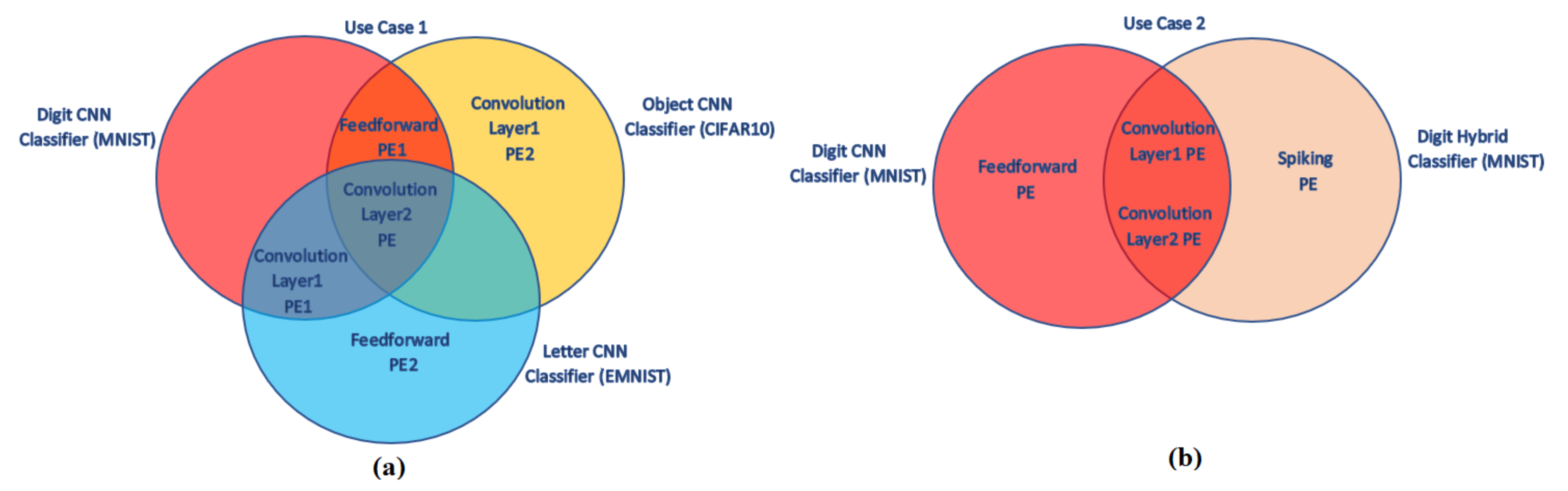
For the proof of concept, two different use cases are implemented on the hardware. In the first use case, three different CNN classifiers trained by three different datasets are designed and switched using DPR for two different scenarios. In the first scenario, a digit classifier trained by the MNIST dataset [27] and a letter classifier trained by EMNIST dataset [
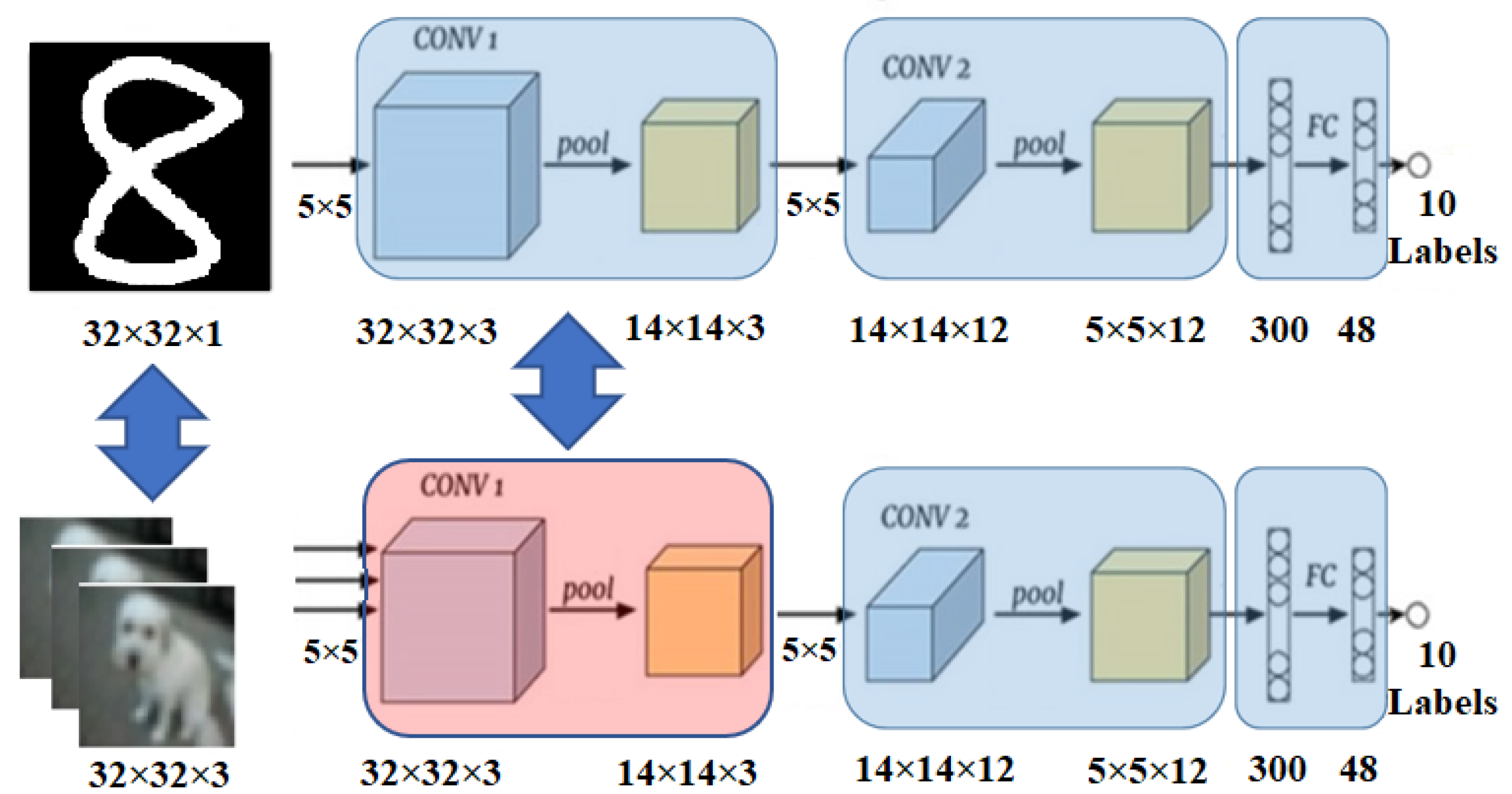
28] are switched only updating the feedforward layers since the number of classes is different between digit and letter classifiers. In the second scenario, a digit classifier trained by MNIST and an object classifier trained by CIFAR10 dataset [29] are switched by updating the first convolution layer because the dataset for digit classifier is grayscale whereas the object dataset is an RGB image. Thus, the number of input channels is different, and the first convolutional layers are required to be different. In both scenarios, the weights and biases of the structurally identical layers are updated from the memory-mapped interface of the PEs and the non-identical layers are dynamically partially reconfigured with the corresponding 
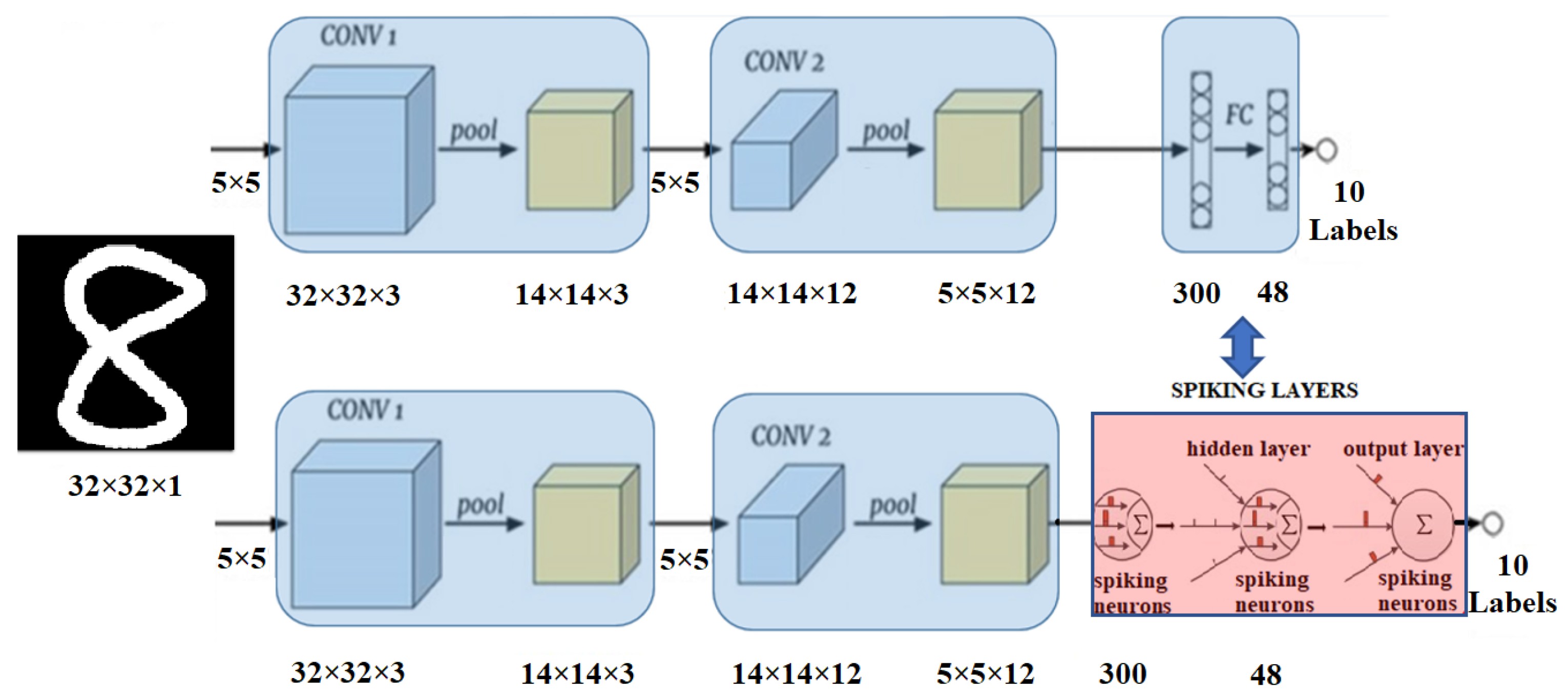
PE. In the second use case, DPR is used to switch between a CNN classifier and a hybrid NN (i.e., consisting of convolutional layers and spiking layers) classifier. Both classifiers are digit classifiers and the convolutional layers of both classifiers have the same structure and use the same weights and bias values. The switching between CNN to hybrid NN is achieved by updating the feedforward layers with spiking layers. The summary of both use cases is given in Figure 12. In this figure, intersection parts show the common layers for the classifiers (i.e., static regions) whereas the other parts show the layers specific to the related classifier (i.e., dynamic regions).

3.1. Use Case 1: CNN to CNN for Different Datasets

The proposed architecture can be used to switch between the same type of NN architectures used for the classification of different classes. Since different NN classifiers can have different number of output classes or different number of input channels, an NN architecture may not be used as-is for the recognition of another class set even if weights and biases are changed for the new classification problem. In other words, at least the input or the output layer should be changed if there is a change in the input or the output parameters, respectively. Therefore, in this use case, we investigate both alternatives (i.e., a change in the number of input channels and a change in the number of output classes) using different scenarios.

3.1.1. Digit Classifier to Letter Classifier Scenario

In the first scenario, we have two different CNN classifiers having a different number of classes. The digit classifier is classifying the ten digits trained by the MNIST dataset. On the other hand, a letter classifier is used to classify the 26 letters in the English alphabet, trained by the EMNIST dataset. The CNN structure of the digit and letter classifiers can be seen in Figure 13. Except for the weights and biases, the only difference between the digit and the letter classifier is the feedforward layers. Without implementing the whole design and reloading the whole bitstream, only implementing a feedforward PE for the letter classifier and updating only a small part of the FPGA with partial bitstream is enough to switch the letter classifier. To put it another way, using the proposed architecture, it can be switched between digit classifier to letter classifier in a very short period of time without waiting for the reconfiguration of the whole FPGA.
As shown in Figure 13, the input of the CNNs is a 32 × 32 8-bit grayscale image, and the output is the classification result. Each CNN accelerator consists of two convolutional layers, two max-pooling layers, a hidden feedforward layer, and an output layer. ReLU activation function is used in the convolutional and hidden layers. In convolutional layers, the convolutional kernel and pooling kernel are selected as 5 × 5 and 2 × 2 for their better performance as compared to other size kernels. In the pooling layers, the downsampling factor is selected as 2. After the convolutional layers, data is flattened and fed to the feedforward layers. In the letter classifier, 48 nodes and ten nodes are used for hidden and output layers, respectively. For the letter classifier, 96 nodes and 26 nodes are used for the hidden and output layers, respectively. The switching between accelerators is achieved by updating the partial bitstreams corresponding to the feedforward layers of the related CNN.

3.1.2. Digit Classifier to Object Classifier Scenario

The second scenario is based on the differences in the input format. Especially in image classification applications, various datasets may have different image formats such as grayscale, RGB, IR, and hyperspectral. Thus, the first convolutional layers are designed according to the data format of the image. In this scenario, digit classifier and object classifier are switched using DPR only by updating the first convolutional layer, since object classifier is trained with CIFAR10 dataset consisting of three-channel colored image (i.e., RGB) whereas digit classifier has single-channel grayscale image dataset for training. Both datasets have ten classes so the other layers are in the same structure (i.e., second convolutional layers and feedforward layers). The CNN structure of the digit and object classifiers can be seen in Figure 14. Note that, weights and biases also differ between the two CNN accelerators but they are updated through the memory-mapped interface of the PE.
As shown in Figure 14, the digit classifier has the same structure as in Figure 13, however, the object classifier RGB input format is 32 × 32 × 3. In other words, in the first convolutional layer, the digit classifier has 1 input image and 3 output feature maps whereas the object classifier has 3 input images and 3 output feature maps. Thus, to realize the object classifier, the convolutional PE for layer 1 is updated from the digit classifier implementation using DPR and in the order of milliseconds, both classifiers can be switched between each other using partial bit files.

3.2. Use Case 2: CNN to Hybrid for Different Architectures

Each NN architecture has its own advantages that can be accuracy, throughput, power consumption, or lower complexity. Thus, in some scenarios, it can be preferred to use the same hardware resources to realize different NN designs, and switch between them without reconfiguring the whole FPGA. Thus, in the second use case, we opt to switch between different NN architectures using the proposed hardware architecture and DPR. To do so, a digit classifier trained by the MNIST dataset is implemented with two different NN architecture. The first architecture is a CNN architecture which is explained above in Use Case 1 whereas the second architecture is a hybrid NN which is a concatenation of convolutional layers and spiking layers. In this architecture, feature maps are first extracted using the convolutional layers, and then these feature maps are fed to the spiking layers for the classification of the digits. The details of these NNs are given in Figure 15.

3.3. Implementation

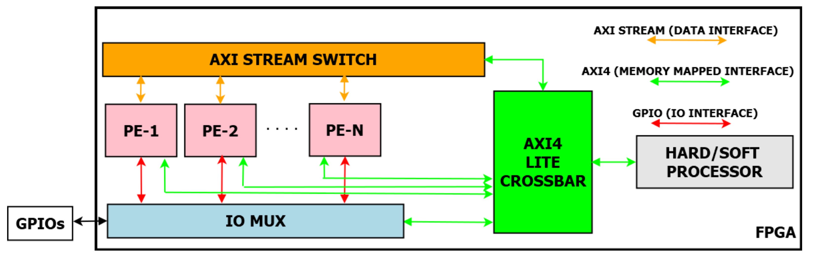
The proposed hardware architecture in Figure 4 is implemented using Xilinx Vivado 2020.2. Using the proposed hardware architecture, two different use cases and three different scenarios explained in the previous section are implemented. In total, 5 different PEs are designed to realize those scenarios. Except for the spiking PE which is a pure VHDL design, all PEs are designed using the Vitis HLS tool, which is used to transform C, C++, and System C codes into the register transfer level implementations [30]. The PE designs are first verified in the simulation environment. Then, they are implemented and tested on a Zedboard FPGA board [31] which is equipped with a Xilinx Zynq 7020 FPGA. The summary of the resource usage of each PE can be seen in Table 1. As shown in Table 1, the resource usage is dominated by the Convolution PEs in the NN architectures. In addition, Feedforward PEs use moderate DSP usage with the minimum deployment of LUTs and FFs since the main computation is the matrix multiplication in Feedforward PEs. On the other hand, the Spiking PE does not use any DSPs because there is no multiplication in the spiking layers. However, it consumes more logical resources, such as LUTs and FFs.
In each scenario, to switch one classifier to the other classifier, only a single PE is updated using DPR. However, for another application, more than a single 
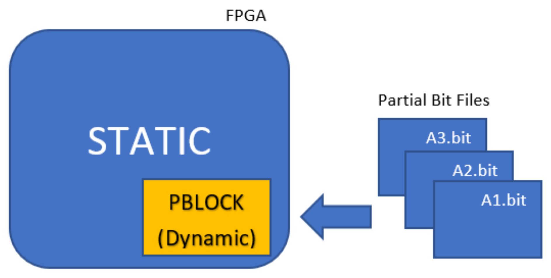
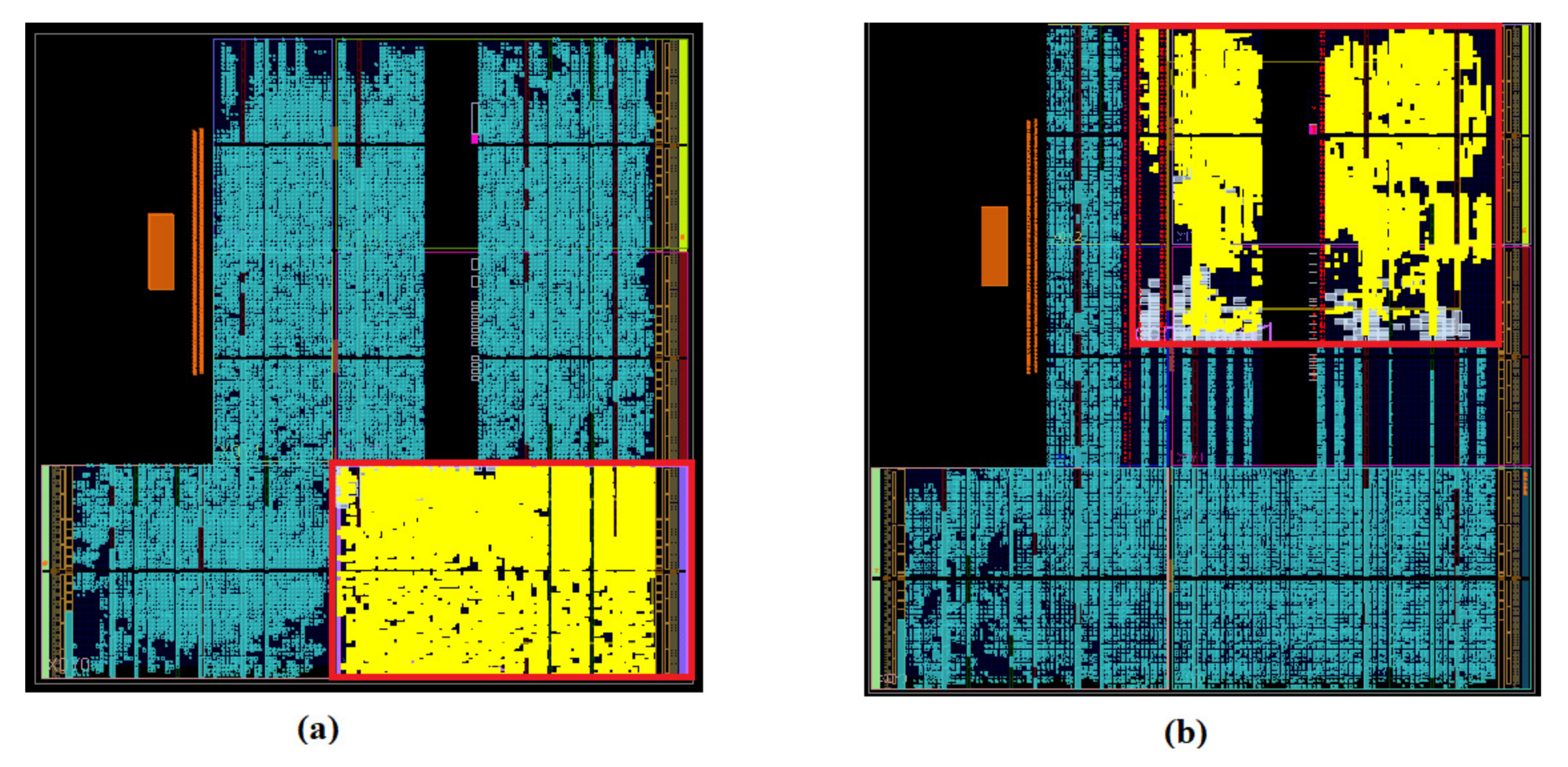
PE could be updated as well. For the DPR, Vivado’s partial reconfiguration flow is used. The size and location of the Pblock of the corresponding PE is determined according to the resource utilization of the related layer of the NN accelerator. In the use cases, two different Pblocks are defined. The first Pblock is for the last layer of Digit CNN Classifier/Digit Hybrid Classifier/Letter CNN Classifier. The second Pblock is for the first layer of Digit CNN Classifier/Object CNN Classifier. Except for the Pblock, the remaining layout of the implementation is static. Thus, only Pblock is placed and routed again for the new scenario realizations. The layout of the implemented NN classifiers and the location of the related Pblocks can be seen in Figure 16.
In the hardware tests of the scenarios, the input images are loaded from the serial port of the Zedboard and the results are written to the registers of the final PE in the chain. The registers are read from the memory-mapped interface of the PE. In addition, the internal data transfers between PEs are tested on the system using Vivado Hardware Manager. All the implementations operate at 100-MHz clock frequency. Table 2 provides resource usages of the classifier accelerator implementations: Digit Classifier (CNN), Letter Classifier (CNN), Object Classifier (CNN), and Digit Classifier (CNN + SNN). In this table, the hybrid classifier DSP usage is the lowest since spiking layers do not use any DSP because there is no multiplication operation in the computation of the spiking layers. However, it consumes more LUTs and FFs since some of the LUTs and FFs are used to convert the feature maps to the spikes in Spiking PE. Moreover, the Digit Classifier CNN uses fewer BRAMs than the other CNNs as it has fewer nodes in the Feedforward PE for the output layer and fewer channels in the Convolution PE for the input layer. Lastly, the Object classifier has the highest DSP usages among them because three-channel classifiers require more multiplications in the input layer in comparison with the one-channel classifiers.

3.4. Evaluation

To conduct a fair performance evaluation of the proposed architecture, we compare the performance of our digit CNN classifier with three state-of-the-art digit CNN classifiers, trained by the MNIST dataset and using the same CNN architecture (i.e., two convolutional layers, two pooling layers, one hidden layer). The first accelerator is a static CNN accelerator [32]. In that study, a ZCU102 evaluation board is used for the implementation. For each convolutional layer and pooling layer, separate accelerators are designed. The second accelerator is a DPR design, and according to the energy level of the power source, the processing system uploads the required partial bitstream at run time using ICAP [17]. The last work is using cascaded connections of processing engines designed to compute the convolution [33]. Pipelining and tiling techniques are used to improve the performance of that design. The performance comparison with these digit classifier accelerators is given in Table 3. As can be seen from Table 3, our proposed digit classifier accelerator has the shortest processing time to complete the classification of an image due to the hardware optimizations in the PE designs that allow for a considerable throughput improvement with using less number of DSPs in comparison with the other accelerators. However, the LUT usage is slightly higher than the other designs because of the implementation of the components for the flexibility of the proposed hardware architecture.
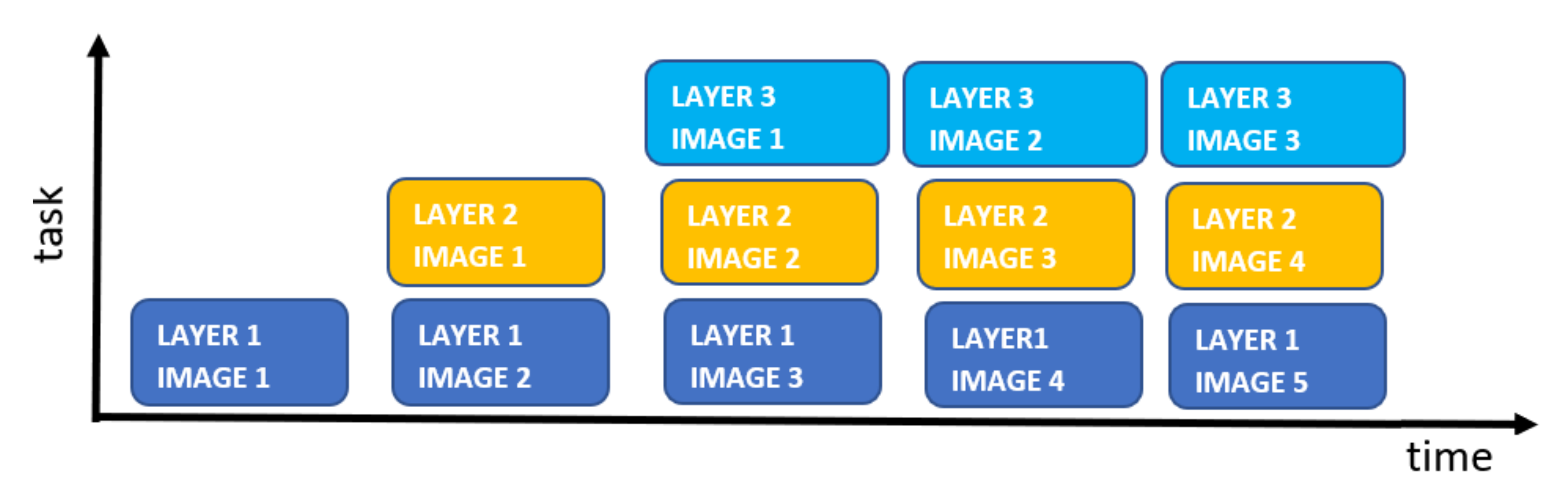
In the proposed architecture, all data is processed in a pipelined manner. Although the total processing time is 62 μ s for the digit classifier; the accelerator can be fed with a higher frame rate. Every PE can process new data after finishing its task, i.e., there is no need to wait until the end of the overall processing of one image to proceed with the next. As shown in Figure 17, the overall frame rate only depends on the processing time of the PE with the largest delay which is 22 μ s (processing time of Feedforward PE for the digit classifier CNN). Therefore, using the pipelining in Figure 17, the proposed accelerator architecture achieves frame rates of up to 45K images/sec in digit classification which is 7× higher than the state-of-the-art digit classifier accelerators given in Table 3.
Using the DPR concept in the proposed architecture has two main advantages. Firstly, instead of training different datasets together, realizing specialized classifiers as different NN greatly increases the accuracy in each task. Table 4 shows the accuracy of three different implementations. In this table, the Character Classifier-1 is a mixed static CNN accelerator trained with both letter and digit datasets together. On the other hand, Digit Classifier and Letter Classifier in Figure 13 are two distinct CNNs. The switching between the digit classifier and the letter classifier is achieved using DPR, reconfiguring only some network layers. The accuracy of the Character Classifier-1 drops by 5% and 10% compared to the specialized letter and the digit neural network models. The increased difficulty causes this drop in performance for a single neural network that needs to learn multiple tasks.
The second advantage of using DPR is the reduction in power consumption. Without sacrificing the accuracy and throughput, a NN design can be realized by using separate Feedforward PEs for digit classifier and letter classifier respectively. Since the proposed architecture allows to change the connection at run time, the classifier can be switched to the related Feedforward PE by updating the connections in the AXI stream switch in the proposed architecture. Thus, the accuracy and execution times remain the same as the digit and letter classifiers given in Figure 13. However, instantiating both Feedforward PEs in the same implementation results in an increase in resource usage and power consumption compared with the DPR implementations as shown in Table 5. In the table, Character Classifier-2 is a classifier design instantiating the Feedforward PEs of the digit classifier and letter classifier in the same implementation. Thus, as clearly seen from Table 5, using DPR makes the design more energy- and resource-efficient compared with the design having both Feedforward PEs. There is a 7% and a 10% decrease in the power consumption of programmable logic in DPR designs as compared to the static design having digit and letter classifiers together. For the power consumption of the processor side, since the processor is running with the same frequency with the same software architecture, the power consumption is 1528 mW and is the same for all classifiers. These consumptions are taken by Vivado’s power report of the implemented (i.e., post-routed) design.
There are also some disadvantages of using DPR. First of all, using DPR increases the difficulty of the design process. The size of the Pblock is to be defined well considering the resource usage of the related PEs. Moreover, defining multiple Pblocks requires a careful placement that should allow easy routing and prevent congestion. However, these design difficulties are coped with only once and the location and size of the Pblocks will probably not be updated unless there are major changes in the design. Besides, another disadvantage of the DPR can be the power overhead during partial reconfiguration. However, as compared with the total reconfiguration of the FPGA, DPR has negligible overhead in terms of power consumption [34]. Similarly, in [35], different experiments were conducted to evaluate the power consumption overhead of DPR for Zynq devices and measurements were done for the processor and the hardware logic fabrics in real-time. In that paper, it is noticed that the power consumed by the FPGA is almost unaffected when applying DPR. Thus, it can be concluded that the proposed method has no significant power or energy overhead while realizing different NN accelerators using DPR.
Lastly, in the proposed architecture, the switch time between digit and letter classifiers (i.e., DPR time) is 9.4 ms, and the switch time between digit and object classifiers is 17.1 ms since the PCAP throughput is 145 MB/s [36] and the partial bit file sizes are 1.37 MB and 2.48 MB for the Pblocks given in Figure 16, respectively. However, for full configuration time of Zedboard is around 250 ms [31]. Therefore, the proposed method can be effectively used, especially in time-critical applications, without wasting the time for updating the whole bitstream. The system can be switched in a very short period of time between digit and letter classifiers only updating the partial bitstream. To do so, in a short response time, the characters can be identified with higher accuracy as compared to the static character classifier designs. However, when the switching between different classifiers is very frequent, the throughput performance may be degraded by the DPR overhead. Since the size of the partial bistream is directly proportional to the size of the region it is reconfiguring, using smaller Pblock may help to decrease the DPR time. In addition, DPR overhead can also be decreased using compressed partial bit files. Yet, these optimizations have limited improvement on DPR overhead and in order to preserve higher overall throughput, the number of switchings between different classifiers should be kept minimal.

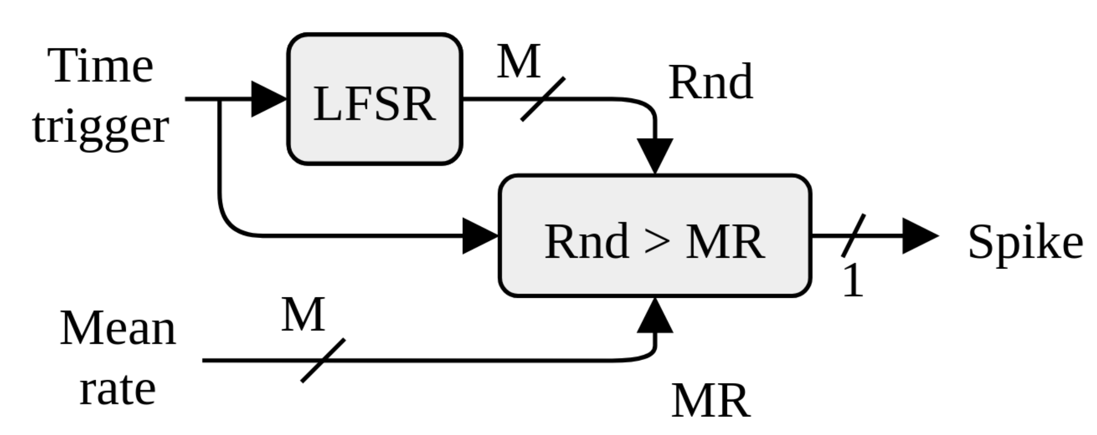
3.5. Evaluation of the Spiking PE

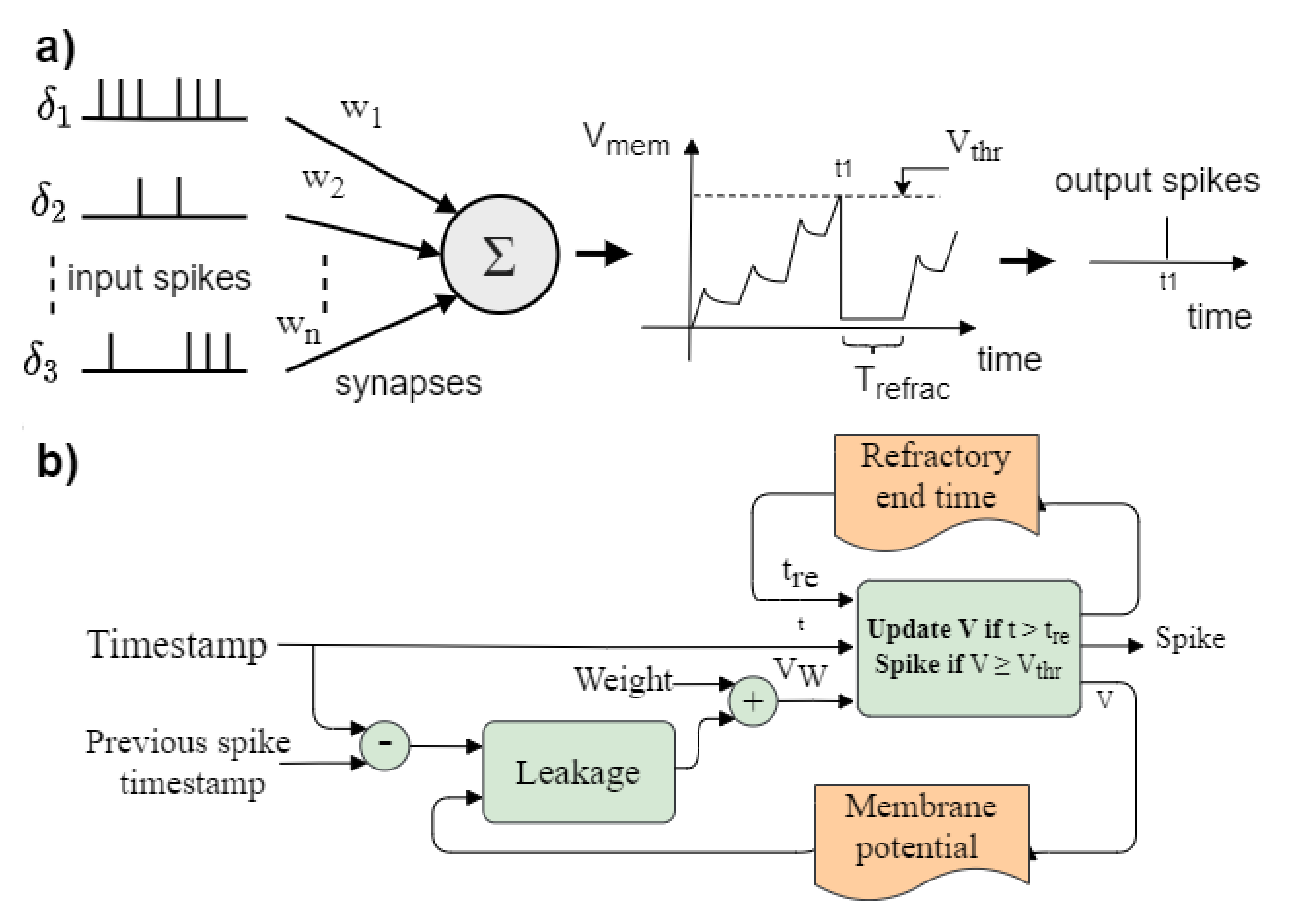
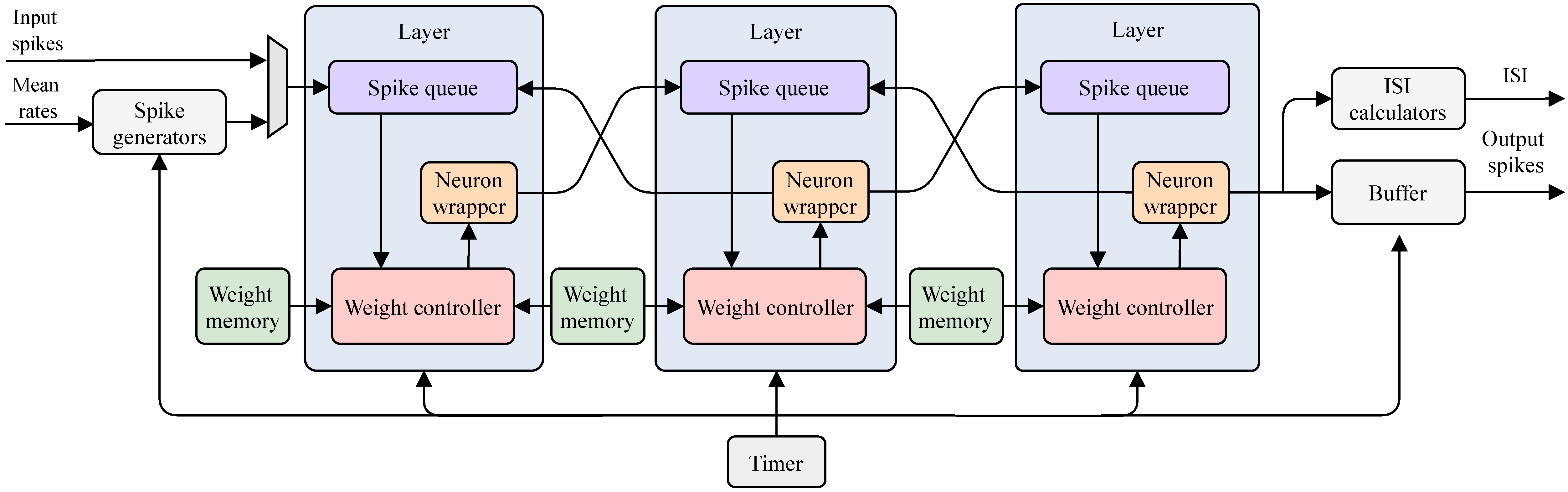
This section compares the spiking PE alone when solving MNIST digit recognition with other spike-based neural network implementations in FPGA. We have implemented a feed-forward network of four layers connected to the 784 input pixels from the MNIST images. The layer size is 784-720-720-720-10. Input has been provided with the mean-rate generators on board, and the outputs have been evaluated by means of the ISI calculators blocks. The spiking PE achieves an accuracy of 99.3 % and a peak-throughput of 40.71 Giga Synaptic Operation Per second (GSOPS) with an efficiency of 0.050 nJ/SO. For comparison, Table 6 shows a list of recently reported spiking neural networks implemented in FPGA. The Bluehive project [37] from Cambridge University implemented 256,000 Izhikevich neurons with 1000 synapses each by interconnecting four FPGAs that each contains 64,000 neurons. Minitaur [9] and its improved version n-Minitaur [38] build upon [39] and operate event-driven. They both time-multiplex 32 physical Leaky-Integrate-and-Fire (LIF) neurons to emulate at a maximum of 65,536 neurons. Note that this is the only purely event-driven implementation in the reported work. In [40] the Efficient Neuron Architecture (ENA) is proposed, which consists of layers of neurons that communicate using packets. Using the LIF model and 32-bit precision, it promises to emulate 3982 neurons and 400 k synapses. The authors implemented only three neurons, though. In [41] an FPGA Design Framework (FDF) is proposed that time-multiplexes up to 200,000 neurons with one physical conductance-based neuron. Furthermore, a network is presented that consists of 1.5 M neurons and 92 G synapses on an FPGA. Only the most significant bits of the exponential decay are stored to reduce memory usage, and the least significant bits are stochastically generated. The same authors emulate 20 M to 2.6 B neurons in a so-called Neuromorphic Cortex Simulator (NCS) [42] using only one FPGA. There is a significant drop in performance, which is likely a result of using off-chip memory, but that increases the supported network size.
Digital ASIC implementations supporting spiking networks and can be extremely power- and energy-efficient [45,46,47]. In ODIN [45], an open-source digital implementation of a spiking neural network core is presented. ODIN’s design only supports one physical neuron core, but many (virtual) neurons can be simulated. Neuron states, as well as synaptic weights, are stored in an on-chip SRAM memory. A state machine takes care of time-multiplexing multiple virtual neurons and executes them in one physical core sequentially. This choice results in a low-area and low power design with the number of events per Synaptic Operation (SOP), which is in the order of ∼10 pJ/SOP at about 100 Mhz. ODIN has demonstrated an accuracy of 91.9 % on MNIST using 4-bit synapses and one physical neuron simulating 256 virtual neurons. In contrast, our spiking PE achieved 99.3 % accuracy on MNIST—a significantly better result achieved through the fully parameterized digital implementation tailored to high-level abstraction designs. The behavior agreement on application and RTL level allows the application specialist to optimize the number of bits per synaptic contact, threshold parameters, and network structure (number of neurons and layers) for better accuracy with fewer resources. Special attention is paid to the memory allocation of synaptic weights to provide the required throughput with minimal resources. Another recent digital ASIC has been presented by Intel [46], and it is named Loihi neuromorphic processor. The Loihi processor exploits a similar concept in which a neuron core emulates many (virtual) up to 1024 neurons and many (virtual) synaptic connections. Time-multiplexing methods exploit timing slack provided by digital silicon speed and constantly shuffle neuron’s membrane potential and synaptic weight memory from/to a central memory. The Loihi architecture hosts multi-neuron cores whose role is the emulation of a part of the network, e.g., a layer, which can exchange spikes asynchronously in a packet-switched form through a network-on-chip (NoC). The advantage of the time-multiplexing approach is a higher neuron and synapse density because the computational core is implemented only once, and the neuron states and synaptic weights are stored in very dense memories. However, in contrast to distributed neuron networks, time-multiplexed networks’ performance and energy efficiency are limited by memory bandwidth and lack of parallelism. The distributed neurons offer a high degree of parallelism and reduce the overhead of data movement caused by shuffling of neuron’s membrane potential in exchange for manageable area overhead. Furthermore, the low-power functionality can also be achieved with distributed neurons through voltage scaling, power gating, and clock gating. For these reasons, our spiking PE architecture does not time-multiplex neurons and exploits a layered organization. Another recent digital spiking neural network architecture called μ Brain has been presented in [47]. The μ Brain also physically implements each neuron and does not use time-multiplexing, achieving microwatt power consumption for an always-on system of 336 neurons with 19,878 synapses while performing MNIST or radar-based gesture classification tasks.

4. Conclusions

In this work, high-performance and flexible NN accelerator architecture is proposed and implemented on an FPGA platform. Moreover, DPR is deployed to realize different NN accelerators with updating only a part of the FPGA implementation. To compute the layers in different NN architectures, different PEs with having the same interfaces are designed. Thus, using these PEs with DPR concept makes the design very efficient particularly for scenarios switching between different NN accelerators in a short period of time and without implementing the whole project again. In addition, the proposed architecture and DPR methodology are illustrated with different use cases to explain the concept in detail. Lastly, the proposed architecture is evaluated by using one of the use cases (i.e., digit classifier) with comparing other state-of-the-art methods. The results showed that the proposed digit classifier achieves higher throughput with moderate DSP and BRAM usage in comparison with previous implementations on FPGAs.

Author Contributions

Conceptualization, H.I., N.A. and D.Z.; methodology, H.I., N.A. and D.Z.; software, H.I. and P.D.; validation, H.I., F.C. and P.D.; formal analysis, H.I. and F.C.; investigation, H.I.; data curation, H.I. and F.C.; writing—original draft preparation, H.I. and F.C.; writing—review and editing, H.I., F.C., P.D., N.A. and D.Z.; visualization, H.I. and F.C.; supervision, N.A. and D.Z.; project administration, H.I.; funding acquisition, H.I. and F.C. All authors have read and agreed to the published version of the manuscript.

Funding

This research was supported in part by The Scientific and Technological Research Council of Turkey (TUBITAK). This research was also supported in part by the ECSEL Joint Undertaking (JU) under grant agreement No 826610. The JU receives support from the European Union’s Horizon 2020 research and innovation programme and Spain, Austria, Belgium, Czech Republic, France, Italy, Latvia, The Netherlands.

Data Availability Statement

No new data were created or analyzed in this study. Data sharing is not applicable to this article.

Conflicts of Interest

The authors declare no conflict of interest.

Abbreviations

The following abbreviations are used in this manuscript:
ASICApplication Specific Integrated Circuit
CNNConvolutional Neural Network
CPUCentral Processing Unit
DMADirect Memory Access
DNNDeep Neural Network
DPRDynamic Partial Reconfiguration
ENAEfficient Neuron Architecture
FDFFPGA Design Framework
FIFOFirst In First Out
FPGAField-Programmable Gate Array
GSOPSGiga Synaptic Operation per Second
ICAPInternal Configuration Access Port
ISIInter Spike Interval
LFSRLinear-Feedback Shift Register
LIFLeaky-Integrate-and-Fire Neuron
NNNeural Network
PCAPProcessor Configuration Access Port
PEProcessing Element
ReLURectified Linear Unit
SNNSpiking Neural Network
SOPSynaptic Operation
SRAMStatic Random Access Memory

References

  1. Wan, Z.; Yu, B.; Li, T.Y.; Tang, J.; Zhu, Y.; Wang, Y.; Raychowdhury, A.; Liu, S. A survey of fpga-based robotic computing. IEEE Circuits Syst. Mag. 2021, 21, 48–74. [Google Scholar] [CrossRef]
  2. Madroñal, D.; Palumbo, F.; Capotondi, A.; Marongiu, A. Unmanned Vehicles in Smart Farming: A Survey and a Glance at Future Horizons. In Proceedings of the 2021 Drone Systems Engineering and Rapid Simulation and Performance Evaluation: Methods and Tools, Budapest, Hungary, 18–20 January 2021; pp. 1–8. [Google Scholar]
  3. Vestias, M.; Neto, H. Trends of CPU, GPU and FPGA for high-performance computing. In Proceedings of the 2014 24th International Conference on Field Programmable Logic and Applications (FPL), Munich, Germany, 2–4 September 2014; pp. 1–6. [Google Scholar]
  4. Rungsuptaweekoon, K.; Visoottiviseth, V.; Takano, R. Evaluating the power efficiency of deep learning inference on embedded GPU systems. In Proceedings of the 2017 2nd International Conference on Information Technology (INCIT), Nakhonpathom, Thailand, 2–3 November 2017; pp. 1–5. [Google Scholar]
  5. Shawahna, A.; Sait, S.M.; El-Maleh, A. FPGA-based accelerators of deep learning networks for learning and classification: A review. IEEE Access 2018, 7, 7823–7859. [Google Scholar] [CrossRef]
  6. Umuroglu, Y.; Fraser, N.J.; Gambardella, G.; Blott, M.; Leong, P.; Jahre, M.; Vissers, K. Finn: A framework for fast, scalable binarized neural network inference. In Proceedings of the 2017 ACM/SIGDA International Symposium on Field-Programmable Gate Arrays, Monterey, CA, USA, 22–24 February 2017; pp. 65–74. [Google Scholar]
  7. Indiveri, G.; Liu, S.C. Memory and information processing in neuromorphic systems. Proc. IEEE 2015, 103, 1379–1397. [Google Scholar] [CrossRef] [Green Version]
  8. Corradi, F.; Adriaans, G.; Stuijk, S. Gyro: A Digital Spiking Neural Network Architecture for Multi-Sensory Data Analytics. In Proceedings of the 2021 Drone Systems Engineering and Rapid Simulation and Performance Evaluation: Methods and Tools, Budapest, Hungary, 18–20 January 2021; pp. 9–15. [Google Scholar]
  9. Neil, D.; Liu, S. Minitaur, an Event-Driven FPGA-Based Spiking Network Accelerator. IEEE Trans. Very Large Scale Integr. (VLSI) Syst. 2014, 22, 2621–2628. [Google Scholar] [CrossRef]
  10. Rueckauer, B.; Lungu, I.A.; Hu, Y.; Pfeiffer, M.; Liu, S.C. Conversion of continuous-valued deep networks to efficient event-driven networks for image classification. Front. Neurosci. 2017, 11, 682. [Google Scholar] [CrossRef] [PubMed]
  11. Xilinx. Partial Reconfiguration User Guide. Available online: https://www.xilinx.com/support/documentation/sw_manuals/xilinx14_7/ug702.pdf (accessed on 25 June 2021).
  12. Koch, D.; Torresen, J.; Beckhoff, C.; Ziener, D.; Dennl, C.; Breuer, V.; Teich, J.; Feilen, M.; Stechele, W. Partial reconfiguration on FPGAs in practice—Tools and applications. In Proceedings of the ARCS 2012, Munich, Germany, 28–29 February 2012; pp. 1–12. [Google Scholar]
  13. Farhadi, M.; Ghasemi, M.; Yang, Y. A Novel Design of Adaptive and Hierarchical Convolutional Neural Networks using Partial Reconfiguration on FPGA. In Proceedings of the 2019 IEEE High Performance Extreme Computing Conference (HPEC), Waltham, MA, USA, 24–26 September 2019; pp. 1–7. [Google Scholar] [CrossRef] [Green Version]
  14. Seyoum, B.B.; Pagani, M.; Biondi, A.; Balleri, S.; Buttazzo, G. Spatio-Temporal Optimization of Deep Neural Networks for Reconfigurable FPGA SoCs. IEEE Trans. Comput. 2020. [Google Scholar] [CrossRef]
  15. Kästner, F.; Janßen, B.; Kautz, F.; Hübner, M.; Corradi, G. Hardware/Software Codesign for Convolutional Neural Networks Exploiting Dynamic Partial Reconfiguration on PYNQ. In Proceedings of the 2018 IEEE International Parallel and Distributed Processing Symposium Workshops (IPDPSW), Vancouver, BC, Canada, 21–25 May 2018; pp. 154–161. [Google Scholar] [CrossRef]
  16. Skrimponis, P.; Pissadakis, E.; Alachiotis, N.; Pnevmatikatos, D. Accelerating Binarized Convolutional Neural Networks with Dynamic Partial Reconfiguration on Disaggregated FPGAs. In Parallel Computing: Technology Trends; IOS Press: Amsterdam, The Netherlands, 2020; pp. 691–700. [Google Scholar]
  17. Youssef, E.; Elsemary, H.A.; El-Moursy, M.A.; Khattab, A.; Mostafa, H. Energy Adaptive Convolution Neural Network Using Dynamic Partial Reconfiguration. In Proceedings of the 2020 IEEE 63rd International Midwest Symposium on Circuits and Systems (MWSCAS), Springfield, MA, USA, 9–12 August 2020; pp. 325–328. [Google Scholar] [CrossRef]
  18. Qin, Z.; Yu, F.; Xu, Z.; Liu, C.; Chen, X. CaptorX: A Class-Adaptive Convolutional Neural Network Reconfiguration Framework. IEEE Trans. Comput. Aided Des. Integr. Circuits Syst. 2021. [Google Scholar] [CrossRef]
  19. Meloni, P.; Deriu, G.; Conti, F.; Loi, I.; Raffo, L.; Benini, L. A high-efficiency runtime reconfigurable IP for CNN acceleration on a mid-range all-programmable SoC. In Proceedings of the 2016 International Conference on ReConFigurable Computing and FPGAs (ReConFig), Cancun, Mexico, 30 November–2 December 2016; pp. 1–8. [Google Scholar] [CrossRef]
  20. Irmak, H.; Alachiotis, N.; Ziener, D. An Energy-Efficient FPGA-based Convolutional Neural Network Implementation. In Proceedings of the 2021 29th Signal Processing and Communications Applications Conference (SIU), Istanbul, Turkey, 9–11 June 2021; pp. 1–4. [Google Scholar]
  21. Irmak, H.; Ziener, D.; Alachiotis, N. Increasing Flexibility of FPGA-based CNN Accelerators with Dynamic Partial Reconfiguration. In Proceedings of the 2021 International Conference on Field-Programmable Logic and Applications (FPL), Virtual Conference, 30 August–3 September 2021; pp. 1–6, (accepted for publication). [Google Scholar]
  22. Wang, Y.; Li, Y.; Song, Y.; Rong, X. The influence of the activation function in a convolution neural network model of facial expression recognition. Appl. Sci. 2020, 10, 1897. [Google Scholar] [CrossRef] [Green Version]
  23. LeCun, Y.; Bottou, L.; Bengio, Y.; Haffner, P. Gradient-based learning applied to document recognition. Proc. IEEE 1998, 86, 2278–2324. [Google Scholar] [CrossRef] [Green Version]
  24. Krizhevsky, A.; Sutskever, I.; Hinton, G.E. Imagenet classification with deep convolutional neural networks. Adv. Neural Inf. Process. Syst. 2012, 25, 1097–1105. [Google Scholar] [CrossRef]
  25. Simonyan, K.; Zisserman, A. Very deep convolutional networks for large-scale image recognition. arXiv 2014, arXiv:1409.1556. [Google Scholar]
  26. Hu, R.; Tian, B.; Yin, S.; Wei, S. Efficient hardware architecture of softmax layer in deep neural network. In Proceedings of the 2018 IEEE 23rd International Conference on Digital Signal Processing (DSP), Shanghai, China, 19–21 November 2018; pp. 1–5. [Google Scholar]
  27. Deng, L. The mnist database of handwritten digit images for machine learning research [best of the web]. IEEE Signal Process. Mag. 2012, 29, 141–142. [Google Scholar] [CrossRef]
  28. Cohen, G.; Afshar, S.; Tapson, J.; Van Schaik, A. EMNIST: Extending MNIST to handwritten letters. In Proceedings of the 2017 International Joint Conference on Neural Networks (IJCNN), Anchorage, AK, USA, 14–19 May 2017; pp. 2921–2926. [Google Scholar]
  29. Krizhevsky, A.; Hinton, G. Learning Multiple Layers of Features from Tiny Images. Available online: http://citeseerx.ist.psu.edu/viewdoc/download?doi=10.1.1.222.9220&rep=rep1&type=pdf (accessed on 25 June 2021).
  30. Vitis High-Level Synthesis. Available online: https://www.xilinx.com/products/design-tools/vivado/integration/esl-design.html (accessed on 25 June 2021).
  31. Zedboard. Available online: https://www.avnet.com/wps/portal/us/products/avnet-boards/avnet-board-families/zedboard/ (accessed on 25 June 2021).
  32. Shi, Y.; Gan, T.; Jiang, S. Design of Parallel Acceleration Method of Convolutional Neural Network Based on FPGA. In Proceedings of the 2020 IEEE 5th International Conference on Cloud Computing and Big Data Analytics (ICCCBDA), Chengdu, China, 10–13 April 2020; pp. 133–137. [Google Scholar]
  33. Li, Z.; Wang, L.; Guo, S.; Deng, Y.; Dou, Q.; Zhou, H.; Lu, W. Laius: An 8-bit fixed-point CNN hardware inference engine. In Proceedings of the 2017 IEEE International Symposium on Parallel and Distributed Processing with Applications and 2017 IEEE International Conference on Ubiquitous Computing and Communications (ISPA/IUCC), Guangzhou, China, 12–15 December 2017; pp. 143–150. [Google Scholar]
  34. Nafkha, A.; Louet, Y. Accurate measurement of power consumption overhead during FPGA dynamic partial reconfiguration. In Proceedings of the 2016 International Symposium on Wireless Communication Systems (ISWCS), Poznan, Poland, 20–23 September 2016; pp. 586–591. [Google Scholar]
  35. Rihani, M.A.; Nouvel, F.; Prévotet, J.C.; Mroue, M.; Lorandel, J.; Mohanna, Y. Dynamic and partial reconfiguration power consumption runtime measurements analysis for ZYNQ SoC devices. In Proceedings of the 2016 International Symposium on Wireless Communication Systems (ISWCS), Poznan, Poland, 20–23 September 2016; pp. 592–596. [Google Scholar]
  36. Xilinx. Zynq-7000 All Programmable Soc: Technical Reference Manual. ug585, v1. 8.1. 2014. Available online: https://www.xilinx.com/support/documentation/user_guides/ug585-Zynq-7000-TRM.pdf (accessed on 25 June 2021).
  37. Moore, S.W.; Fox, P.J.; Marsh, S.J.T.; Markettos, A.T.; Mujumdar, A. Bluehive—A field-programable custom computing machine for extreme-scale real-time neural network simulation. In Proceedings of the 2012 IEEE 20th International Symposium on Field-Programmable Custom Computing Machines, Toronto, ON, Canada, 29 April–1 May 2012; pp. 133–140. [Google Scholar] [CrossRef] [Green Version]
  38. Kiselev, I.; Neil, D.; Liu, S. Event-driven deep neural network hardware system for sensor fusion. In Proceedings of the 2016 IEEE International Symposium on Circuits and Systems (ISCAS), Montreal, QC, Canada, 22–25 May 2016; pp. 2495–2498. [Google Scholar] [CrossRef]
  39. O’Connor, P.; Neil, D.; Liu, S.; Delbruck, T.; Pfeiffer, M. Real-time classification and sensor fusion with a spiking deep belief network. Front. Neurosci. 2013, 7, 178. [Google Scholar] [CrossRef] [PubMed] [Green Version]
  40. Wan, L.; Luo, Y.; Song, S.; Harkin, J.; Liu, J. Efficient neuron architecture for FPGA-based spiking neural networks. In Proceedings of the 2016 27th Irish Signals and Systems Conference (ISSC), Londonderry, UK, 21–22 June 2016; pp. 1–6. [Google Scholar] [CrossRef]
  41. Wang, R.; Hamilton, T.J.; Tapson, J.; van Schaik, A. An FPGA design framework for large-scale spiking neural networks. In Proceedings of the 2014 IEEE International Symposium on Circuits and Systems (ISCAS), Melbourne, Australia, 1–5 June 2014; pp. 457–460. [Google Scholar] [CrossRef]
  42. Wang, R.M.; Thakur, C.S.; van Schaik, A. An FPGA-Based Massively Parallel Neuromorphic Cortex Simulator. Front. Neurosci. 2018, 12, 213. [Google Scholar] [CrossRef] [PubMed] [Green Version]
  43. Pani, D.; Meloni, P.; Tuveri, G.; Palumbo, F.; Massobrio, P.; Raffo, L. An FPGA Platform for Real-Time Simulation of Spiking Neuronal Networks. Front. Neurosci. 2017, 11, 90. [Google Scholar] [CrossRef] [PubMed]
  44. Han, J.; Li, Z.; Zheng, W.; Zhang, Y. Hardware implementation of spiking neural networks on FPGA. Tsinghua Sci. Technol. 2020, 25, 479–486. [Google Scholar] [CrossRef]
  45. Frenkel, C.; Lefebvre, M.; Legat, J.D.; Bol, D. A 0.086-mm2 12.7-pJ/SOP 64k-synapse 256-neuron online-learning digital spiking neuromorphic processor in 28-nm CMOS. IEEE Trans. Biomed. Circuits Syst. 2018, 13, 145–158. [Google Scholar] [PubMed] [Green Version]
  46. Davies, M.; Srinivasa, N.; Lin, T.H.; Chinya, G.; Cao, Y.; Choday, S.H.; Dimou, G.; Joshi, P.; Imam, N.; Jain, S.; et al. Loihi: A neuromorphic manycore processor with on-chip learning. IEEE Micro 2018, 38, 82–99. [Google Scholar] [CrossRef]
  47. Stuijt, J.; Sifalakis, M.; Yousefzadeh, A.; Corradi, F. μBrain: An Event-Driven and Fully Synthesizable Architecture for Spiking Neural Networks. Front. Neurosci. 2021, 15, 538. [Google Scholar] [CrossRef] [PubMed]
Figure 1. The Concept of Partial Reconfiguration.
Jlpea 11 00032 g001
Figure 2. Interfaces of the Processing Element.
Jlpea 11 00032 g002
Figure 3. NN PE Types.
Jlpea 11 00032 g003
Figure 4. Proposed hardware architecture with multiple PEs.
Jlpea 11 00032 g004
Figure 5. Convolution Operation in CNNs.
Jlpea 11 00032 g005
Figure 6. Block Diagram of the Proposed Convolution.
Jlpea 11 00032 g006
Figure 7. Feedforward NN structure.
Jlpea 11 00032 g007
Figure 8. Leaky-Integrate-and-Fire (LIF) neuron model. (a) Behavior of the neuron. (b) Digital behavior, neurons receive spikes in the form of a timestamp. It integrates them if it is not in the refractory period. It would emit a spike if the membrane potential exceeded the threshold. The leakage block is implemented with a bit shift for resource savings.
Jlpea 11 00032 g008
Figure 9. Spiking Neural Network PE. Spiking PE architecture is organized in layers of fully connected spiking neurons that are executed in parallel.
Jlpea 11 00032 g009
Figure 10. Spike buffer sharing mechanism.
Jlpea 11 00032 g010
Figure 11. Spike generation with stochastic ISI.
Jlpea 11 00032 g011
Figure 12. Summary of Use Cases: (a) Same NN architecture with Different Classifiers, (b) Different NN architectures for Digit Classifier.
Jlpea 11 00032 g012
Figure 13. Digit classifier and letter classifier, and the switching between them using DPR.
Jlpea 11 00032 g013
Figure 14. Digit classifier and object classifier, and the switching between them using DPR.
Jlpea 11 00032 g014
Figure 15. CNN and Hybrid architectures and switching between each other using DPR.
Jlpea 11 00032 g015
Figure 16. The layout of the implemented classifier accelerators. The red rectangles correspond to the partial reconfigurable areas (i.e., Pblocks), yellow color shows the dynamic part, and cyan color shows the static part of the designs: (a) Digit CNN Classifier/Digit Hybrid Classifier/Letter CNN Classifier (b) Digit CNN Classifier/Object CNN Classifier.
Jlpea 11 00032 g016
Figure 17. Pipelined processing of the Digit Classifier Accelerator.
Jlpea 11 00032 g017
Table 1. Resource usage of different PEs.
ClassifierBRAMDSPLUTFF
Convolutional PEDigit/Letter Classifier Layer 1173442584604
Convolutional PEObject Classifier Layer 1214774856382
Convolutional PEDigit/Letter/Object Classifier Layer 21511313,89411,893
Feedforward PEDigit Classifier8.520810740
Feedforward PELetter Classifier2020601616
Spiking PEDigit Classifier21053138931
Table 2. Resource usage of different classifier accelerators, The numbers in parenthesis show the utilization on Zedboard.
BRAMDSPLUTFF
Digit Classifier (CNN)58.5 (42%)167 (76%)24,980 (47%)27,925 (26%)
Letter Classifier (CNN)70 (50%)167 (76%)24,771 (47%)27,801 (26%)
Object Classifier (CNN)62.5 (45%)180 (82%)27,402 (52%)29,496 (28%)
Digit Classifier (CNN + SNN)71 (51%)147 (67%)31,093 (58%)37,698 (35%)
Table 3. Performance Comparison of Different Digit Classifiers.
BRAMDSPLUTProcessing TimeFPGA Model
Shi [32]5420425,276170 μsZynq UltraScale+ 9EG
Youssef [17]9N/A19,141270 μsZynq 7020
Li [33]6199169071490 μsVirtex7 485t
This work58.516724,98062 μsZynq 7020
Table 4. Comparison of Digit Classifier, and Letter Classifier with Character Classifier-1 in terms of resource usage and accuracy on Zedboard (Zynq7020).
BRAMDSPLUTAccuracyExecution Time
Character Classifier 1 (Static)7016725,11787.5387.55 μ s
Letter Classifier (DPR)7016724,77192.4584.92 μ s
Digit Classifier (DPR)58.516724,98098.8862.19 μ s
Table 5. Comparison of Digit Classifier, and Letter Classifier with Character Classifier-2 in terms of resource usage and power consumption.
BRAMDSPLUTPower Consumption (Programmable Logic)
Character Classifier-27918726,5251231 mW
Letter Classifier7016724,7711123 mW
Digit Classifier58.516724,9801146 mW
Table 6. FPGA-based spiking neural network implementations in chronological order.
NameBluehiveFDFn-MinitaurPaniNCSTsinghuaThis Work
Reference[37][41][38][43][42][44]N/A
Year2012201420162017201820202021
FPGAStratix IVVirtex 6Spartan 6Virtex 6Stratix VZynq 7000Zynq Ultrascale+
Clock (MHz)200266105100200200250
Neuron modelIzhikevichConductanceLIFIzhikevichLIFLIFLIF
NetworkUnknownUnknownFeed-forwardRecurrentUnknownFeed-forwardRecurrent
DrivenTime-drivenTime-drivenEvent-drivenTime-drivenTime-drivenHybridEvent-driven
Weight storageOff-chipOn-chipOff-chipOn-chipOff-chipOff-chipOn-chip
Weight bit-width12 bits12 bits16 bits7 bits4 bits16 bits6 bits
Cores1623328200 kUnknownSame as neurons
Number of neurons256 k1.5 M17941440100 M28422954
Time resolution1 ms0.32 msN/A0.1 ms1 msN/AN/A
Peak throughput (GSOPS)0.25612000.05350.0144200.6740.71
Power dissipation (W)UnknownUnknown1.58.532.40.52.039
Energy efficiency (nJ/SO)UnknownUnknown285901.627120.050
MNIST accuracyUnknownUnknown94.1%UnknownUnknown97.1%99.3%
Publisher’s Note: MDPI stays neutral with regard to jurisdictional claims in published maps and institutional affiliations.

