
The Design Methodology of Fully Digital Pulse Width Modulation


Department of Electrical Engineering, Princess Sumaya University for Technology, Amman 11941, Jordan
J. Low Power Electron. Appl. 2021, 11(4), 41; https://0-doi-org.brum.beds.ac.uk/10.3390/jlpea11040041
Submission received: 14 September 2021
/
Revised: 19 October 2021
/
Accepted: 19 October 2021
/
Published: 21 October 2021
Abstract
:This paper describes the design methodology and calibration technique for a low-power digital pulse width modulation demodulator to enhance its robustness against the process, voltage, and temperature variations in different process corners, in addition to intra-die variability, which makes it a very good choice for implantable monitoring sensors. Furthermore, the core of the proposed demodulator is fully digital. Thus, along with the proposed design methodology, the proposed demodulator can be simply redesigned in advanced subnanometer CMOS technologies without much difficulty as compared to analog demodulators. The proposed demodulator consists of an envelope detector, a digitizer, a ring oscillator, and a data detector with digital calibration. All the proposed circuits are designed and simulated in the standard 1P9M TSMC’s 40 nm CMOS technology. Simulation results have shown that the circuit is capable of demodulating and recovering data from an input signal with a carrier frequency of 13.56 MHz and a data rate of 143 kB/s with an average power consumption of 5.62 W.
1. Introduction
Diabetes is a lifelong metabolic disorder that weakens the human body’s ability to process blood sugar. Building up sugars in the blood can lead to serious complications such as stroke, blindness, heart diseases, kidney failure, and lower limb amputation. Despite diabetes being an incurable condition, careful and ongoing monitoring of diabetes along with appropriate diet and medication can help patients to stay healthy. The diabetes incidence rate is increasing every year, and according to the World Health Organization (WHO) report (2021), there are approximately 422 million confirmed cases worldwide, mostly in low- and middle-income countries [1,2]. It is expected that over 693 million people will be exposed to this lifetime disease by 2045 if proper actions are not taken [3,4].
The most effective drug for controlling the blood glucose level of diabetics is insulin, and this drug needs to be delivered to the blood. Traditional methods for delivering insulin to the human blood usually involve some form of invasive injection or oral therapy and these are regarded as painful or unpleasant by most patients [5,6]. To overcome this problem and enhance adherence to insulin regimens, transdermal drug delivery (TDD) has been widely used. TDD stands out as a more favorable option, due to its non-invasive and painless approach. It is accomplished by increasing the permeability of the skin to insulin, through which insulin can be applied and then absorbed, eventually entering the blood. This method offers an important advantage due to the ease of accessibility to the skin and has attracted the attention of researchers and diabetics [7,8].
The skin consists of two main layers: the epidermis and the dermis. The epidermis is divided into two sub-layers which are the stratum corneum and the living epidermis. The outer layer of the skin, the stratum corneum, causes the low permeability of the skin to TDD [9]. Many methods have been used to overcome the low permeability of the skin such as mechanical methods [10] (microneedles, abrasion, perforation, and skin stretching) and electrical-assisted methods [11] (iontophoresis, electroporation, and radiofrequency) [12]. However, other promising physical methods such as ultrasound [13] can be used to increase the permeability of the skin in a phenomenon referred to as sonophoresis [14].
The effectiveness of the ultrasound technique depends on many controlled parameters, such as the intensity, the net exposure time, and the on-off ratio of the in vivo delivery of insulin, but also depends on a number of uncontrolled parameters such as the hair concentration on the skin, the thickness of the stratum corneum, and humidity [15]. These parameters can cause varying levels of insulin absorption through the skin, and the amount of insulin that reaches the blood would be hard to control. In order to overcome this problem, real-time monitoring of the insulin level in the blood can provide a feedback mechanism for accurately controlling the amount of insulin that is injected into the blood. Moreover, if the blood glucose concentration can also be monitored in real-time, it can be used to trigger the injection of insulin automatically. This would allow for the realization of a self-controlled ultrasound system that delivers insulin to the blood automatically according to instant glucose and insulin levels within the blood, without the involvement of the patient. This self-controlled technique deploys implantable glucose and insulin biosensors as the main building blocks of the entire system.
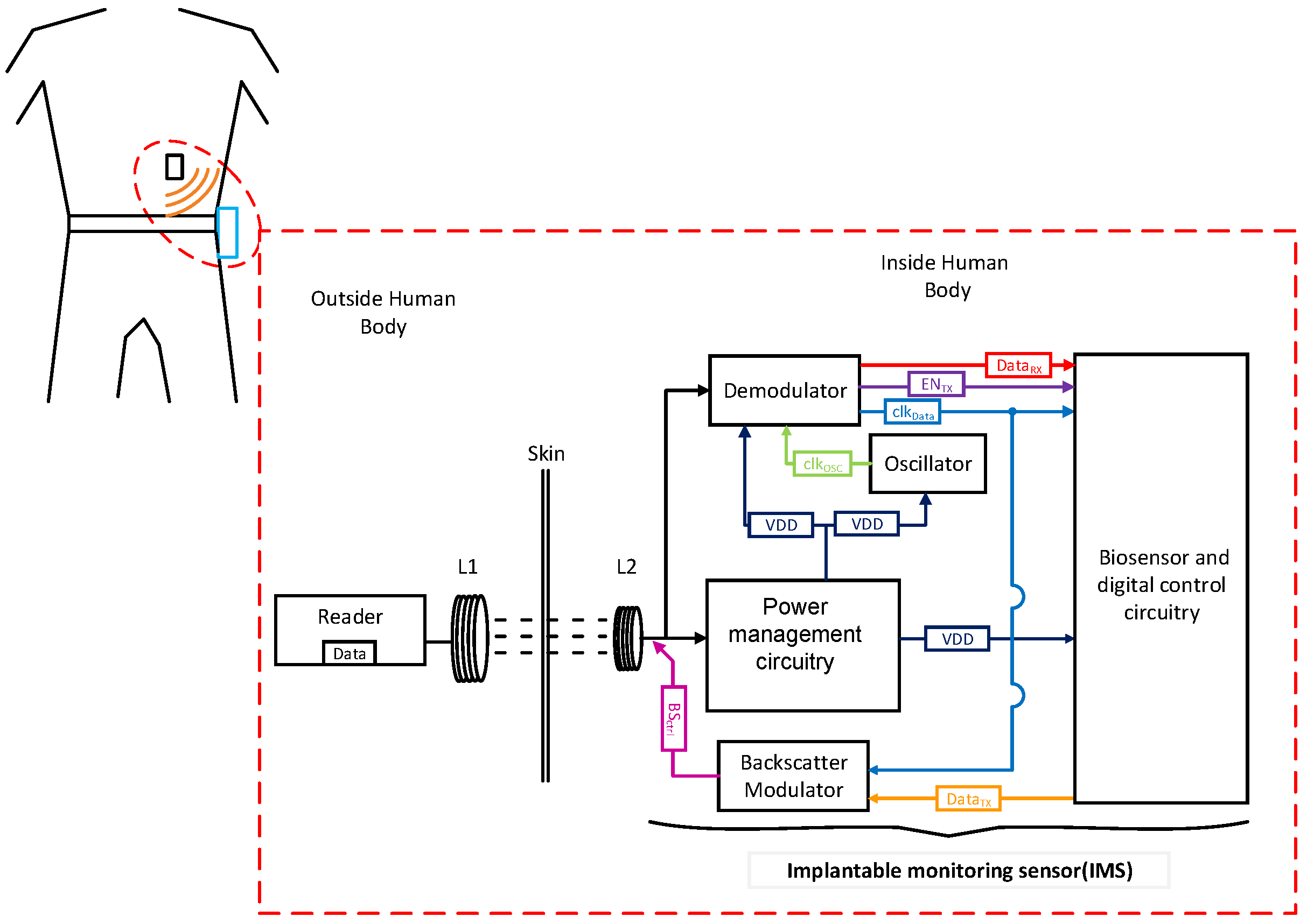
Implantable biosensor devices are of great importance for monitoring internal body parameters such as electrocardiogram data [16], pressure levels [17], gastrointestinal parameter values ( pH, temperature, pressure) [18], and blood glucose [19], to name a few. In these systems, implantable sensor units transmit data to an external reader device and then to a control unit (computer) or a central monitoring unit for data analysis [20].
Figure 1 illustrates a possible implementation for a self-controlled ultrasound insulin delivery system. In the red-dashed box, the portable external reader device transmits a modulating signal through inductive coupling coil L1. The implantable monitoring sensor (IMS) receives the modulating signal through the internal coil (L2). The IMS includes a demodulator, internal clock generator, power management circuitry, biosensor, digital control circuitry, and backscattering modulator.
In IMS, the PWM modulation scheme has been intensively used, primarily because of the low power consumption and the simplicity of its demodulator circuitry [21]. However, designing a demodulator for PWM in advanced CMOS technologies, such as 40 nm, is a challenging issue. This is mainly due to the high sensitivity of advanced CMOS technologies for the process, supply voltage, and temperature variation (PVT), besides intra-die variability [22,23]. On the other hand, the size of the IMS is dominated by on-chip capacitors. A high on-chip capacitance density (metal-oxide-metal capacitor) makes advanced CMOS technologies attractive for IMS [24,25].
This article is a continuation of the author’s work published in [26], where the passive transponder front-end for IMS was proposed. However, the design methodology of the digital PWM demodulator (DPWMD) was not discussed despite its importance. Therefore, this article discusses the design methodology of a low-power DPWMD to enhance its robustness against PVT variations in different process corners. Additionally, a calibration technique is utilized to minimize the impact of PVT variations and intra-die variability. The proposed DPWMD consists of an envelope detector, a digitizer, a ring oscillator, and a data detector with digital calibration. The proposed DPWMD is designed and simulated using 40 nm 1P9M TSMC’s CMOS technology. Simulation results have shown that the circuit is capable of demodulating and recovering data from an input signal with a carrier frequency of 13.56 MHz and a data rate of 143 kB/s with an average power consumption of 5.62 W.
2. Proposed DPWMD
Figure 2 shows the timing diagram of the proposed DPWMD. The top trace shows the typical modeling waveforms of the proposed PWM, each gap representing a clock pulse transition. The duration of the gap represents either a logic “one” or “zero” transition depending on the duration of the gap width. The demodulator interprets long/short durations as logic “one”/“zero”. To solve PVT variations and intra-die variability issues, a calibration mode is introduced. This mode is activated at the beginning of the transmission by sending three successive gaps followed by the calibration gap. The second trace from the top illustrates the extracted data clock (), the third trace from the top depicts the extracted data (), and the bottom trace shows the ring oscillator () that is used to measure the gap duration.
The basic block diagram of the proposed DPWMD is illustrated in Figure 3. The PWM demodulation is done by an envelope detector, a digitizer, a ring oscillator, and a data detector with digital calibration. The implementation details and design considerations are presented in the following sections.
2.1. Envelope Detector
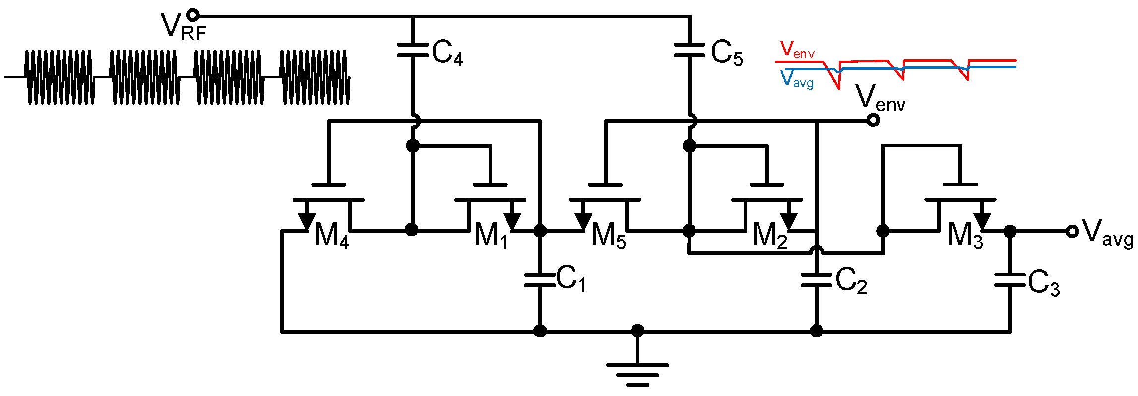
The functionality of the envelope detector circuitry is to generate two output signals: the and its average from the received modulating signal [27], as shown in Figure 4. The three diode-connected devices M1–M3 are used to detect the presence of the gaps in the received modulating signal, and C1–C3 are storage capacitors. During the gap duration, M4 and M5 provide a path to discharge C1 and C2. In addition, to enhance noise immunity, is shifted below through connecting the drains of M2 and M3.
2.2. Digitizer
The digitizer is principally a comparator or more precisely a Schmitt trigger [28]. The digitizer has two switching points: upper and lower trip points UTP and LTP, respectively. When is lower than by the amount of UTP, the output voltage pulse is high. This output voltage continues to be high until rises again above by the amount of LTP. The digitizer generates pulses with variable durations. The presence of the pulse corresponds to a transition in the transmitted data. Thus, the output of the digitizer can be considered as a data clock (). Furthermore, the duration of the pulse can be used to identify whether logic “one” or “zero” has been transmitted. The schematic of the proposed digitizer is depicted in Figure 5.
2.3. Ring Oscillator
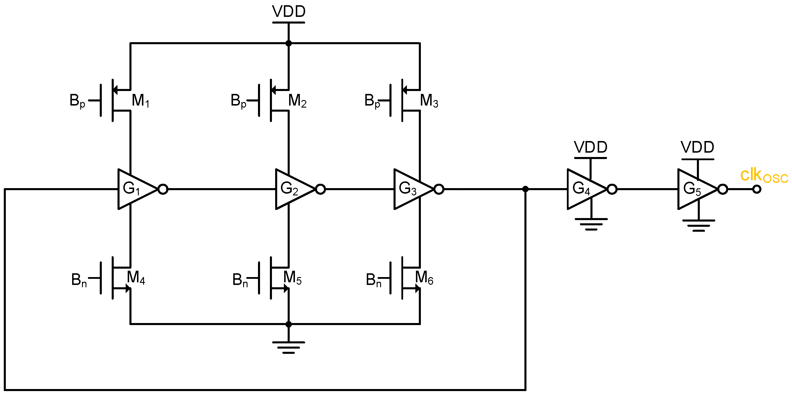
The designed ring oscillator is based on the current-starved inverter structure. As shown in Figure 6, it consists of three starved inverters, G1, G2, and G3, connected in the ring structure followed by a simple inverter, G4 and G5, to sharpen the edges of the output signal (). This circuit provides an on-chip clock signal to measure the duration of the gaps and to distinguish between long and short gaps. However, it is obvious that the frequency of the oscillator is highly effected by PVT variations and intra-die variability issues. Thus, a calibration technique is introduced to solve this issue.
2.4. Data Detector with Digital Calibration
The main function of this block is to distinguish between long and short-duration digitizer output pulses () by using the . To minimize the error due to the PVT variations and the intra-die variability, the binary decision threshold principle has been employed. If the duration of the pulse is greater than or equal to , then the pulse is interpreted as a long gap (logic one). Otherwise, the pulse is interpreted as a short gap (logic zero). This simple methodology minimizes the probability of making an incorrect decision in determining the pulse duration, even with the presence of the PVT variations and the intra-die variability.
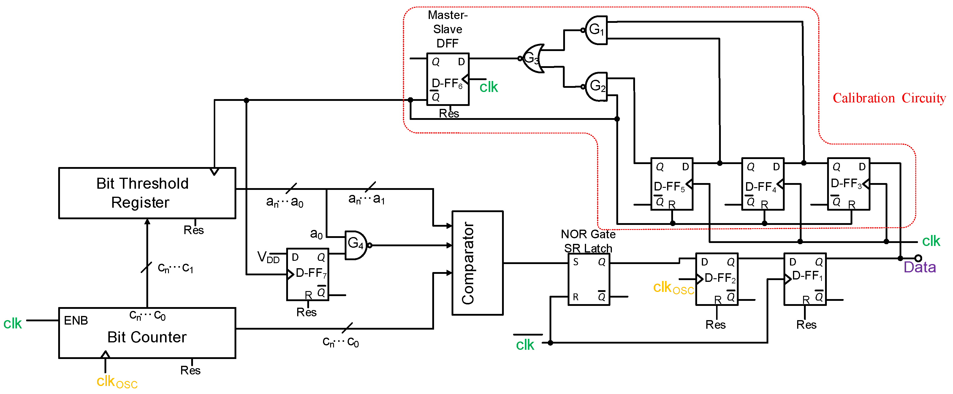
Figure 7 shows the data detector with digital calibration. The gap discrimination is done by a digital counter, a threshold register, a comparator, and a calibration circuitry. The digital counter is clocked by the signal and enabled by the signal. Thus, it counts the duration of the pulse in terms of the pulses. At the end of the duration, the content of the digital counter is . The threshold register stores a binary number () corresponding to . The comparator provides an output that assumes one of two distinct values based on and : high voltage (logic one) when (long pulse) and low voltage (logic zero) when (short pulse). Finally, the calibration circuitry is used to detect the calibration mode pattern which consists of three successive long-duration pulses.
When the calibration circuitry detects the calibration pattern, the threshold register stores the half value of the digital counter which corresponds to the duration of . This can be simply done by transferring the content of the digital counter after dropped the least significant bit (LSB) to the threshold register.
3. Design Issues and System Parameters
This section introduces all the parameters that need to be considered to design the proposed DPWMD, such as the time duration of the gap representing logic zero (), the time duration of the gap representing logic one (), the time duration of the calibration gap (), the size of the digital counter (), and the size of the threshold register ().
As mentioned previously, the time duration of a gap is determined by the digital counter for N clock cycles of the signal. N is an integer number, and it is given for a positive-edge-triggered counter as
where is denoted for the floor function. It is obvious that is highly affected by PVT variations and intra-die variability. Therefore, for a fixed gap duration, N is not defined as a single value, but it is defined as an element in the set of candidate values.
As illustrated in Figure 8, there are three candidate sets of integers: logic zero set is interpreted as a logic zero, logic one set is interpreted as a logic one, and threshold set which used to discriminate between set and . The boundary elements of ( and ) can be described by
where and are the maximum and minimum frequencies of due to PVT variations, respectively. In the same way, the boundary elements of ( and ) can be found by substituting instead of in Equations (2) and (3), respectively. The boundary elements of ( and ) are given as
For proper operation, two conditions must be satisfied: first and second . Thus, must be
where . The above equation implies that . To simply achieve the requirement in Equation (6), is given as
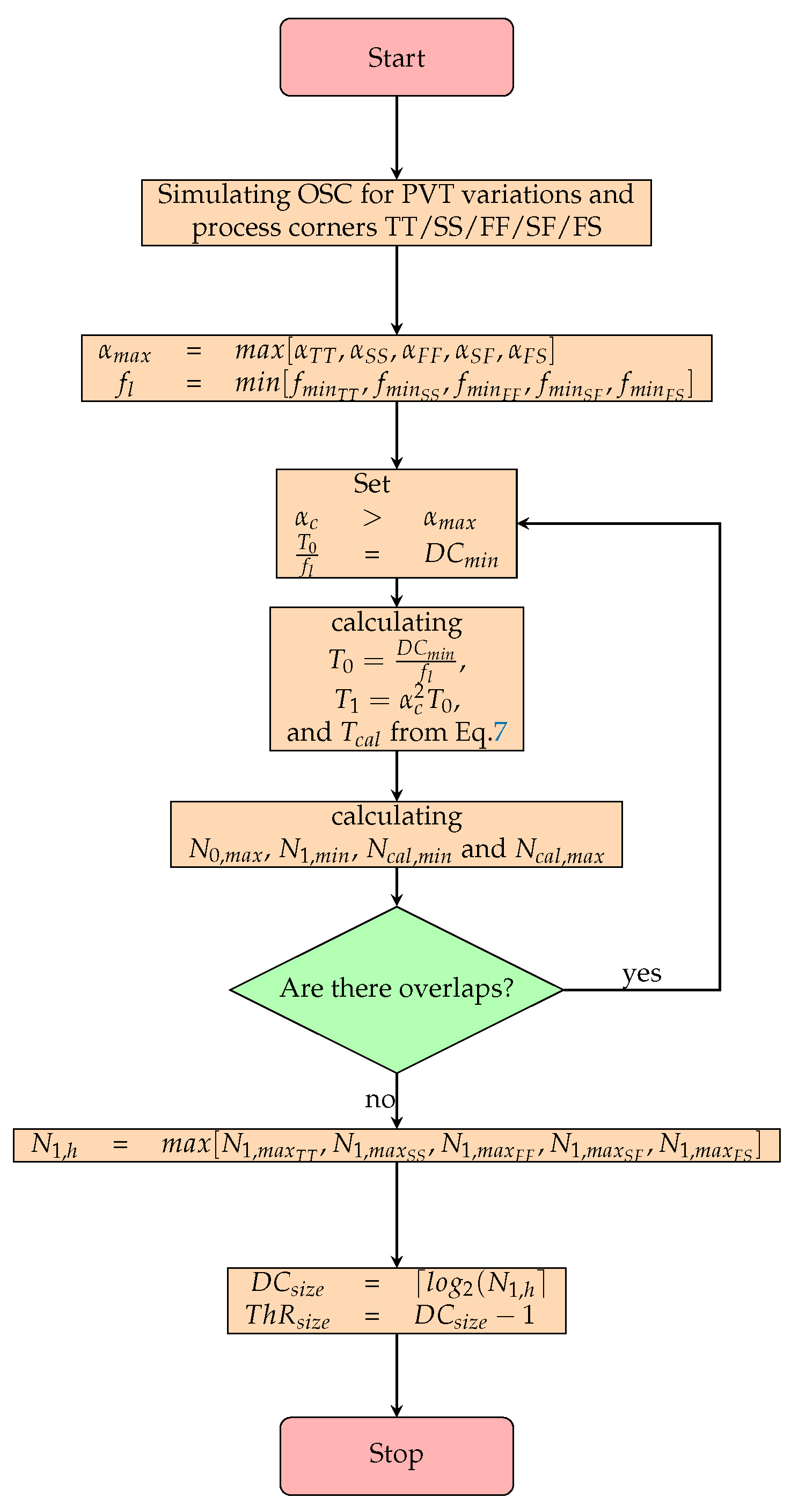
The design methodology of the proposed DPWMD is illustrated in the flowchart shown in Figure 9. In this methodology, the calculation of the parameters is done for the worst-case condition. The first step starts with simulating the ring oscillator for PVT variations in different process corners. Once the simulation results are done, and can be determined as defined in the flowchart. In the next step, is selected to be greater than about . At the same step, the lowest digital counter reading () (that propositional to under low clock frequency condition ()) is defined. It is worth noting that the value of should be less than the bit interval (in our case, 1/(143 kB/s) ≈ 7 s). In addition, to simplify the design of the power management circuitry, should be at least less than 20% of the bit interval to preserve the continuity of the carrier signal [27].
Once the values of , , and are calculated, , , , and can be found as defined in Equations (1)–(5). If , , , and are overlapped, then the assumed values of , , or both of them should be changed. In addition, the previously mentioned steps must be repeated. If there are no overlaps in , , , and , then can be found as defined in the flowchart. In the last step, the size of the counter and the threshold register are determined as defined in the flowchart, where is denoted for the ceiling function.
4. Simulation Results and Discussion
The proposed DPWMD is designed and simulated in 1P9M TSMC’s 40 nm CMOS process technology. The demodulator is simulated with a carrier frequency of 13.56 MHz, a data rate of 143 kB/s, and a nominal supply voltage of 0.9 V.
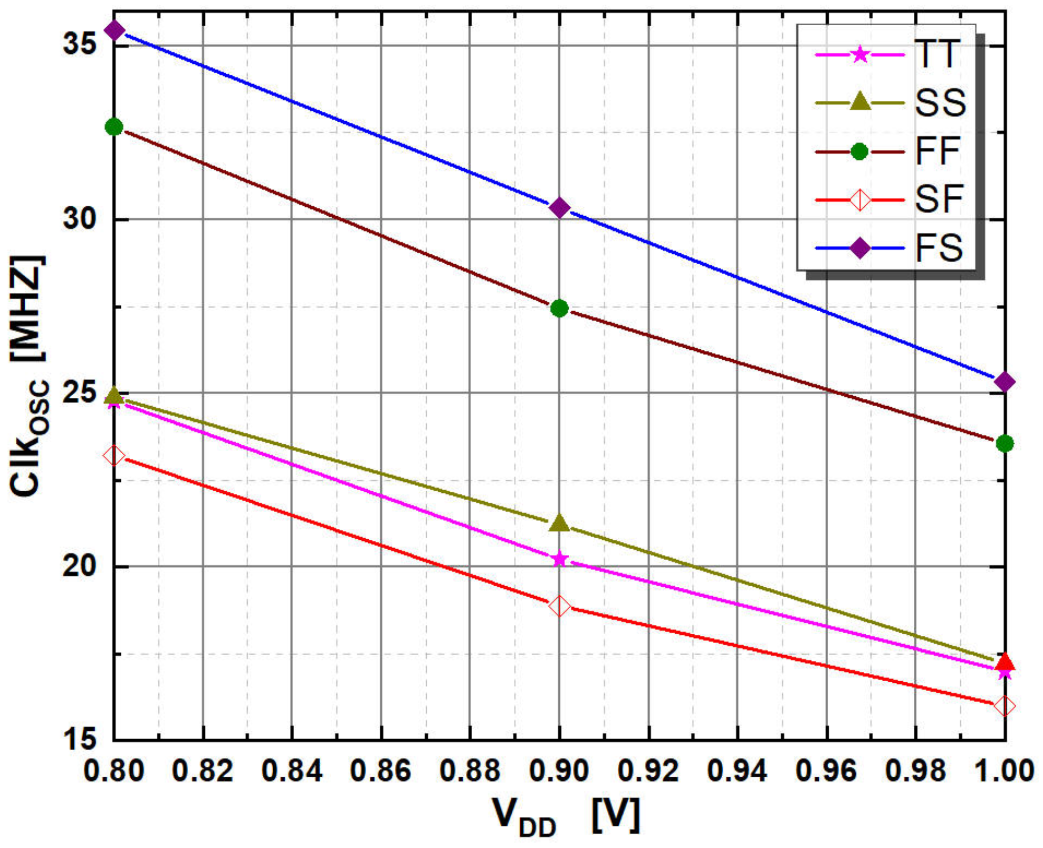
As mentioned earlier, the proposed DPWMD utilizes the ring oscillator’s frequency to measure the duration of the gaps to discriminate between long and short gaps. Thus, for proper operation, the worst-case condition due to PTV variation of the ring oscillator should be identified. However, in IMS, temperature variations are not an issue since the human body temperature is self-regulated [29]. Therefore, the oscillator frequency variations due to supply voltage changes ( mV from the nominal value of 0.9 V) at TT, SS, FF, SF, and FS process corners are simulated, as shown in Figure 10.
To tolerate the frequency variations, the design methodology described in the last section is followed. From the illustrated simulation results, , and MHz, so the values of and have been selected to be and 6, respectively. For the selected values, s, s, and s.
The calculated , , and sets at each process corner are listed in Table 1. As noted, there are no overlaps between sets for the selected values. In addition, the value of . Therefore, the size of the counter and threshold registers have been chosen to be 6 bits and 5 bits, respectively.
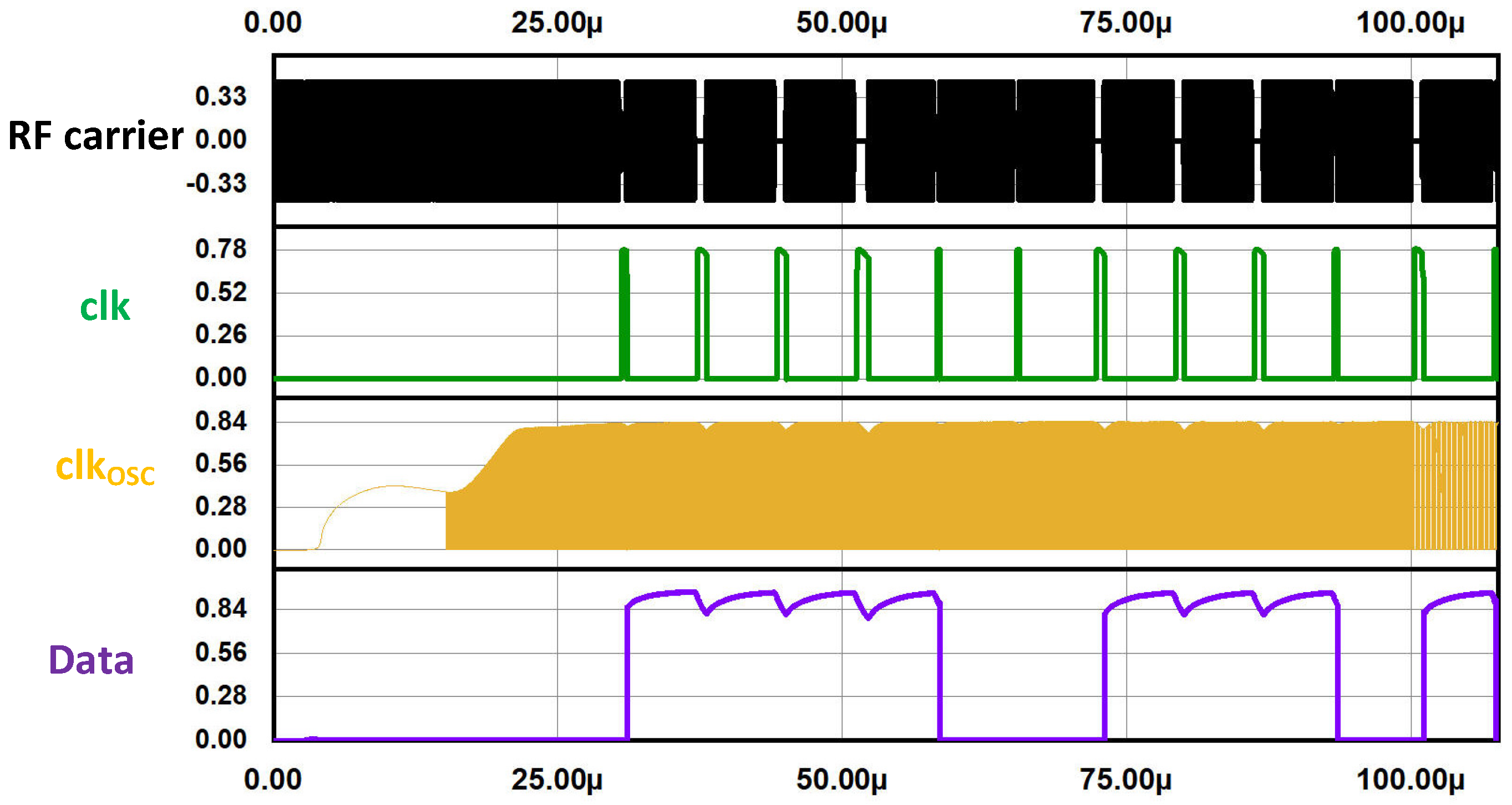
The transient simulation results of the proposed DPWMD are shown in Figure 11. It can be noticed that the proposed DPWMD extracted the data clock () and from the RF carrier signal. The proposed demodulator can function accurately under a supply voltage variation of mV from the nominal value of V. The demodulated signal starts with three successive bits to enable the calibration mode, followed by a calibration pulse. After the calibration pulse period is measured using the internal signal, the proposed demodulation can successfully distinguish between long and short gaps, even with supply voltage variations.
The proposed design has a total average power consumption of 5.62 W. The average power consumption of the demodulator is 3.32 W, while the envelope detector, digitizer, and ring oscillator consume 2.3 W.
Table 2 shows a list of useful and necessary features of the proposed demodulator. A brief comparison is drawn among the different published articles and this work in supporting these features. It is clear from the table summary that the proposed demodulator of this work has a high energy efficiency with an FoM of 39.3 pJ/bit.
5. Conclusions
This paper describes the design methodology and calibration technique for a low-power digital pulse width modulation demodulator to enhance its robustness against the process, voltage, and temperature variations in different process corners, in addition to intra-die variability, which makes it a very good choice for implantable monitoring sensors. The proposed demodulator consists of an envelope detector, a digitizer, a ring oscillator, and a data detector with digital calibration. The transient simulation results showed that the proposed demodulator can function accurately under a supply voltage variation of V from the nominal value of V. Furthermore, the core of the proposed demodulator is fully digital. Thus, along with the proposed design methodology, the proposed demodulator can be simply redesigned in advanced subnanometer CMOS technologies without much difficulty as compared to analog demodulators.
Funding
This research received no external funding.
Data Availability Statement
Data are contained within the article.
Acknowledgments
The author would like to thank EUROPRACTICE for their kind support by providing the Cadence Spectre Circuit Simulator and the technology files.
Conflicts of Interest
The author declares no conflict of interest.
Abbreviations
The following abbreviations are used in this manuscript:
| CMOS | Complementary Metal–Oxide–Semiconductor |
| WHO | World Health Organization |
| PWM | Pulse Width Modulation |
| ASK | Amplitude Shift Keying |
| PPM | Pulse Position Modulation |
| PVT | Process, Voltage, and Temperature Variations |
| TTD | Transdermal Drug Delivery |
| IMS | Implantable Monitoring Sensor |
| DPWMD | Digital PWM Demodulator |
| LSB | Least Significant Bit |
References
- Haque, M.; Islam, S.; Kamal, Z.M.; Akter, F.; Jahan, I.; Rahim, M.S.A.; Sultana, N.; Alam, A.M.; Murshid, M.E.; Halim-Khan, M.; et al. Ongoing efforts to improve the management of patients with diabetes in Bangladesh and the implications. Hosp. Pract. 2021, 1–7. [Google Scholar] [CrossRef]
- Williams, R.; Karuranga, S.; Malanda, B.; Saeedi, P.; Basit, A.; Besançon, S.; Bommer, C.; Esteghamati, A.; Ogurtsova, K.; Zhang, P.; et al. Global and regional estimates and projections of diabetes-related health expenditure: Results from the International Diabetes Federation Diabetes Atlas. Diabetes Res. Clin. Pract. 2020, 162, 108072. [Google Scholar] [CrossRef] [Green Version]
- Lin, X.; Xu, Y.; Pan, X.; Xu, J.; Ding, Y.; Sun, X.; Song, X.; Ren, Y.; Shan, P.F. Global, regional, and national burden and trend of diabetes in 195 countries and territories: An analysis from 1990 to 2025. Sci. Rep. 2020, 10, 14790. [Google Scholar] [CrossRef]
- Zhao, R.; Lu, Z.; Yang, J.; Zhang, L.; Li, Y.; Zhang, X. Drug delivery system in the treatment of diabetes mellitus. Front. Bioeng. Biotechnol. 2020, 8, 880. [Google Scholar] [CrossRef] [PubMed]
- World Health Organization. Guidelines on Second-and Third-Line Medicines and Type of Insulin for the Control of Blood Glucose Levels in Non-Pregnant Adults with Diabetes Mellitus; World Health Organization: Geneva, Switzerland, 2018. [Google Scholar]
- He, X.; Sun, J.; Zhuang, J.; Xu, H.; Liu, Y.; Wu, D. Microneedle system for transdermal drug and vaccine delivery: Devices, safety, and prospects. Dose-Response 2019, 17, 1559325819878585. [Google Scholar] [CrossRef] [PubMed] [Green Version]
- Giudice, E.L.; Campbell, J.D. Needle-free vaccine delivery. Adv. Drug Deliv. Rev. 2006, 58, 68–89. [Google Scholar] [CrossRef] [PubMed]
- Godin, B.; Touitou, E. Transdermal skin delivery: Predictions for humans from in vivo, ex vivo and animal models. Adv. Drug Deliv. Rev. 2007, 59, 1152–1161. [Google Scholar] [CrossRef] [PubMed]
- Prausnitz, M.R.; Langer, R. Transdermal drug delivery. Nat. Biotechnol. 2008, 26, 1261–1268. [Google Scholar] [CrossRef]
- Larrañeta, E.; McCrudden, M.T.; Courtenay, A.J.; Donnelly, R.F. Microneedles: A new frontier in nanomedicine delivery. Pharm. Res. 2016, 33, 1055–1073. [Google Scholar] [CrossRef] [Green Version]
- Vadlapatla, R.; Wong, E.Y.; Gayakwad, S.G. Electronic drug delivery systems: An overview. J. Drug Deliv. Sci. Technol. 2017, 41, 359–366. [Google Scholar] [CrossRef]
- Ahad, A.; Raish, M.; Bin Jardan, Y.A.; Al-Mohizea, A.M.; Al-Jenoobi, F.I. Delivery of Insulin via Skin Route for the Management of Diabetes Mellitus: Approaches for Breaching the Obstacles. Pharmaceutics 2021, 13, 100. [Google Scholar] [CrossRef]
- Miao, Y.Y.; Wang, Z.L.; Zhang, P.Y. New Approach of Transdermal Drug Delivery: Sonophoresis. DEStech Trans. Comput. Sci. Eng. 2018. [Google Scholar] [CrossRef] [Green Version]
- Mitragotri, S.; Blankschtein, D.; Langer, R. Ultrasound-mediated transdermal protein delivery. Science 1995, 269, 850–853. [Google Scholar] [CrossRef]
- Boucaud, A.; Tessier, L.; Machet, L.; Vaillant, L.; Patat, F. Transdermal delivery of insulin using low frequency ultrasound. In Proceedings of the 2000 IEEE Ultrasonics Symposium Proceedings An International Symposium (Cat. No. 00CH37121), San Juan, PR, USA, 22–25 October 2000; Volume 2, pp. 1453–1456. [Google Scholar]
- Heo, J.C.; Kim, B.; Kim, Y.N.; Kim, D.K.; Lee, J.H. Induction of inflammation in vivo by electrocardiogram sensor operation using wireless power transmission. Sensors 2017, 17, 2905. [Google Scholar] [CrossRef] [Green Version]
- Cong, P.; Ko, W.H.; Young, D.J. Integrated electronic system design for an implantable wireless batteryless blood pressure sensing microsystem. IEEE Commun. Mag. 2010, 48, 98–104. [Google Scholar] [CrossRef]
- Sangodoyin, S.; Ugurlu, E.M.; Dey, M.; Prvulovic, M.; Zajic, A. Leveraging On-Chip Transistor Switching for Communication and Sensing in Neural Implants and Gastrointestinal Devices. IEEE Trans. Biomed. Eng. 2021. [Google Scholar] [CrossRef] [PubMed]
- DeHennis, A.; Getzlaff, S.; Grice, D.; Mailand, M. An NFC-enabled CMOS IC for a wireless fully implantable glucose sensor. IEEE J. Biomed. Health Inform. 2015, 20, 18–28. [Google Scholar] [CrossRef] [PubMed]
- Shi, B.; Liu, Z.; Zheng, Q.; Meng, J.; Ouyang, H.; Zou, Y.; Jiang, D.; Qu, X.; Yu, M.; Zhao, L.; et al. Body-integrated self-powered system for wearable and implantable applications. ACS Nano 2019, 13, 6017–6024. [Google Scholar] [CrossRef] [PubMed]
- Lee, W.H.; Lee, Y.T.; Kim, J.W.; Takao, H.; Sawada, K.; Ishida, M. Wireless smart temperature sensor using pulse width modulation method. In Proceedings of the 2007 70th ARFTG Microwave Measurement Conference (ARFTG), Tempe, AZ, USA, 29–30 November 2007; pp. 1–4. [Google Scholar]
- Almeida, R.B.; Marques, C.; Butzen, P.F.; Silva, F.; Reis, R.A.; Meinhardt, C. Analysis of 6 T SRAM cell in sub-45 nm CMOS and FinFET technologies. Microelectron. Reliab. 2018, 88, 196–202. [Google Scholar] [CrossRef]
- Zhang, K.; Chen, Y.N.; Dong, Y.; Xie, Z.Q.; Zhao, Z.F.; Si, P.; Yu, T.Y.; Dai, L.; Lv, W.F. Effect of Random Channel Dopants on Timing Variation for Nanometer CMOS Inverters. In Proceedings of the 2019 IEEE 2nd International Conference on Electronics Technology (ICET), Chengdu, China, 10–13 May 2019; pp. 208–212. [Google Scholar]
- Chiu, P.Y.; Ker, M.D. Metal-layer capacitors in the 65 nm CMOS process and the application for low-leakage power-rail ESD clamp circuit. Microelectron. Reliab. 2014, 54, 64–70. [Google Scholar] [CrossRef]
- Ando, T.; Cartier, E.; Jamison, P.; Pyzyna, A.; Kim, S.; Bruley, J.; Chung, K.; Shobha, H.; Estrada-Raygoza, I.; Tang, H.; et al. CMOS compatible MIM decoupling capacitor with reliable sub-nm EOT high-k stacks for the 7 nm node and beyond. In Proceedings of the 2016 IEEE International Electron Devices Meeting (IEDM), San Francisco, CA, USA, 3–7 December 2016; pp. 9–14. [Google Scholar]
- Shahroury, F.R.; Mohammad, A.A. Design of a passive CMOS implantable continuous monitoring biosensors transponder front-end. Microelectron. J. 2019, 90, 141–153. [Google Scholar] [CrossRef]
- Shahroury, F.R. Design of a low-power CMOS transceiver for semi-passive wireless sensor network application. Integration 2020, 71, 95–104. [Google Scholar] [CrossRef]
- Allen, P.E.; Holberg, D.R. CMOS Analog Circuit Design; Elsevier: Amsterdam, The Netherlands, 2011. [Google Scholar]
- Houdas, Y.; Ring, E. Human Body Temperature: Its Measurement and Regulation; Springer Science & Business Media: New York, NY, USA, 2013. [Google Scholar]
- Zhang, H.; Chen, X.; Chen, M.; Wang, G. A wide-input-range low-power ASK demodulator for wireless data transmission in retinal prosthesis. In Proceedings of the 2016 IEEE Biomedical Circuits and Systems Conference (BioCAS), Shanghai, China, 17–19 October 2016; pp. 492–495. [Google Scholar]
- Ture, K.; Kilinc, E.G.; Maloberti, F.; Dehollain, C. Remotely powered PPM demodulator by inductive coupling for rodent applications. Analog Integr. Circuits Signal Process. 2016, 88, 359–368. [Google Scholar] [CrossRef]
- Lee, H.; Kim, J.; Ha, D.; Kim, T.; Kim, S. Differentiating ASK demodulator for contactless smart cards supporting VHBR. IEEE Trans. Circuits Syst. II Express Briefs 2015, 62, 641–645. [Google Scholar] [CrossRef]
- Fedtschenko, T.; Stanitzki, A.; Kokozinski, R.; Schaal, C.; Müller, K.U.; Utz, A.; Ferres, E. A 13.56 MHz RF Frontend with Current-Mode Demodulator for Wide Input-Power Dynamic-Range. In Proceedings of the 2019 IEEE 39th International Conference on Electronics and Nanotechnology (ELNANO), Kyiv, Ukraine, 16–18 April 2019; pp. 568–571. [Google Scholar]
Figure 1.
The block diagram of self-controlled ultrasound insulin delivery system.

Figure 2.
Waveform timing description of the proposed PWM.

Figure 3.
Implemented DPWMD architecture.

Figure 4.
Schematic of envelope detector.

Figure 5.
Schematic of digitizer.

Figure 6.
Schematic of the ring oscillator based on current-starved inverter structure.

Figure 7.
Schematic of data detector with digital calibration.

Figure 8.
Logic zero set (), logic one set (), and threshold set ().

Figure 9.
Design procedure for the proposed digital PWM demodulator.

Figure 10.
Simulation results of the ring oscillator frequency due to supply voltage variation at each process corner.
Figure 10.
Simulation results of the ring oscillator frequency due to supply voltage variation at each process corner.

Figure 11.
The transient simulation results of proposed demodulator circuit.


Table 1.
The calculated , , and sets at each process corner.
| TT | 6 | 9 | 11 | 16 | 17 | 24 |
| SS | 6 | 9 | 11 | 16 | 17 | 24 |
| FF | 9 | 13 | 15 | 21 | 23 | 32 |
| SF | 6 | 9 | 10 | 15 | 16 | 23 |
| FS | 10 | 14 | 16 | 23 | 25 | 35 |
Table 2.
Performance parameters comparison with the literature.
| [30] | [31] | [32] | [33] | This Work | |
|---|---|---|---|---|---|
| Process node (nm) | 350 | 180 | 180 | 350 | 40 |
| Carrier (MHz) | 13.56 | 13.56 | 13.56 | 13.56 | 13.56 |
| Modulation scheme | ASK | PPM | ASK | ASK | PWM |
| Supply voltage (V) | 3 | 1.8 | 1.8 | 3∼3.6 | 0.9 |
| Data rate (Mbps) | 0.7 | 0.00813 | 6.78 | 0.42375 | 0.143 |
| Power (uW) | 76.5 | 27.8 | 396 | 450 | 5.62 |
| FoM a (pJ/bit) | 109.3 | 3419 | 58.4 | 1062 | 39.3 |
[a] FoM = Power/Data Rate.
Publisher’s Note: MDPI stays neutral with regard to jurisdictional claims in published maps and institutional affiliations. |
© 2021 by the author. Licensee MDPI, Basel, Switzerland. This article is an open access article distributed under the terms and conditions of the Creative Commons Attribution (CC BY) license (https://creativecommons.org/licenses/by/4.0/).
Share and Cite
MDPI and ACS Style
Shahroury, F.R. The Design Methodology of Fully Digital Pulse Width Modulation. J. Low Power Electron. Appl. 2021, 11, 41. https://0-doi-org.brum.beds.ac.uk/10.3390/jlpea11040041
AMA Style
Shahroury FR. The Design Methodology of Fully Digital Pulse Width Modulation. Journal of Low Power Electronics and Applications. 2021; 11(4):41. https://0-doi-org.brum.beds.ac.uk/10.3390/jlpea11040041
Chicago/Turabian StyleShahroury, Fadi R. 2021. "The Design Methodology of Fully Digital Pulse Width Modulation" Journal of Low Power Electronics and Applications 11, no. 4: 41. https://0-doi-org.brum.beds.ac.uk/10.3390/jlpea11040041
Note that from the first issue of 2016, this journal uses article numbers instead of page numbers. See further details here.