Article

A Sub-50 µm2, Voltage-Scalable, Digital-Standard-Cell-Compatible Thermal Sensor Frontend for On-Chip Thermal Monitoring

Department of Electrical Engineering, Columbia University, New York, NY 10032, USA
*
Author to whom correspondence should be addressed.
J. Low Power Electron. Appl. 2018, 8(2), 16; https://0-doi-org.brum.beds.ac.uk/10.3390/jlpea8020016
Submission received: 1 May 2018 / Revised: 23 May 2018 / Accepted: 25 May 2018 / Published: 30 May 2018
(This article belongs to the Special Issue CMOS Low Power Design)

Abstract

:
This paper presents an on-chip temperature sensor circuit for dynamic thermal management in VLSI systems. The sensor directly senses the threshold voltage that contains temperature information using a single PMOS device. This simple structure enables the sensor to achieve an ultra-compact footprint. The sensor also exhibits high accuracy and voltage-scalability down to 0.4 V, allowing the sensor to be used in dynamic voltage frequency scaling systems without requiring extra power distribution or regulation. The compact footprint and voltage scalability enables our proposed sensor to be implemented in a digital standard-cell format, allowing aggressive sensor placement very close to target hotspots in digital blocks. The proposed sensor frontend prototyped in a 65 nm CMOS technology has a footprint of 30.1 µm2, 3σ-error of ±1.1 °C across 0 to 100 °C after one temperature point calibration, marking a significant improvement over existing sensors designed for dynamic thermal management in VLSI systems.

1. Introduction

In today’s microprocessors and Systems-on-Chips (SoC), a temperature sensor is essential for dynamic thermal management (DTM). In DTM, multiple temperature sensors are typically embedded on a chip to monitor and control chip’s thermal behavior so as to ensure performance and reliability [1,2]. Small and accurate temperature sensor design is desired since temperature sensing accuracy is directly dependent on the distance between sensors and hotspots and sensor’s circuit-level accuracy [1,2,3]. Existing sensors achieve impressive area and accuracy [4,5,6,7,8,9,10,11,12,13,14,15,16,17,18,19,20]. However, emerging technology trends toward multicore architectures, 3D-IC, and ultra-dynamic-voltage-scaling (UDVS) make sensor designs to be even more demanding with the following requirements.
First, ultra-compact sensors are required to monitor the increasing number of hotspots and to improve flexibility in placement. The number of thermal hotspots and the degree of thermal gradients have increased with a higher level of transistor integration. This has led modern high-performance microprocessors to embed tens of temperature sensors (e.g., 48 sensors in [21,22,23]). The emerging technology trends toward multicore architectures and 3D-IC can create even more hotspots due to the thermal coupling between cores and 3D layers [1]. To monitor all of hotspots at low hardware overhead, sensor footprint needs to be extremely small [1,2,3]. Further on, the hotspots are often only identified in the later stages of design. Thus, it is highly desirable to make sensors small for maximal flexibility in placement.
The remote sensing approach, as proposed in [8,16,17], can help meet this size requirement. In this approach, each frontend is remotely placed very close to hotspots, yet the backend is shared by multiple frontends and placed in a location away from hot digital-heavy area, the latter being able to simplify the design of the backend as well. In this approach, a frontend of the size of digital standard cells (e.g., 10s of µm2) is ideal to closely monitor hotspots.
Second, while minimizing the sensor size, the sensors need to maintain a small circuit-level error across process and voltage variations to improve thermal sensing accuracy. Overestimating the temperature of the system can cause unnecessary performance throttling. On the other hand, underestimating can raise a reliability concern. This demands high accuracy temperature sensor circuits. Furthermore, such high accuracy is desired to require simple and inexpensive post-silicon calibration, e.g., one temperature point calibration (OPC).
Finally, voltage scalability is important for supporting dynamic voltage frequency scaling (DVFS) systems [24,25]. DVFS systems can provide peak performance when workload is heavy by operating a processor at nominal supply voltage (VDD). DVFS systems can achieve low power by scaling VDD down to near threshold voltage when the workload is moderate or low. For the sensors to be employed without extra voltage distribution or local regulation in such systems, they need to operate across a wide range of VDD.
Classical BJT based sensors [4,5] targeting general temperature sensing applications (e.g., RFID tags) achieves high accuracy (e.g., ±0.15 °C 3σ-error), however, their large area and high supply voltage requirement limit their usage in DTM. Recent BJT based sensor designs [6,7,8,9,17] successfully miniaturize their frontend footprint (as low as 360 µm2 [17]) while meeting a relaxed accuracy requirement for DTM application. However, BJT based sensor designs have limited voltage scalability (e.g., minimum VDD > 1 V) and their size is still one or two orders of magnitude larger than digital standard cells (e.g., 10’s of µm2 or less). Also, BJT is not available in many advanced technologies. As compared to the standard BJT sensors, MOSFET threshold voltage (VTH) based sensors typically achieve a smaller footprint and better voltage scalability [10,11,12,13,14,15,16,17,18]. However, the linearity of VTH against temperature is dependent on the characteristics of the process technology which raises the concern on technology portability of such design. Contrarily, BJT based sensors are less dependent on process technology. As presented in [19,20], thermal-diffusivity (TD) sensors that use diffusivity of bulk silicon for temperature sensing can also achieve less dependency on process technology. Another possible challenge for MOSFET based sensor is aging effects (e.g., negative biasing temperature instability [NBTI]) which can cause long-term accuracy degradation.
In Figure 1, we choose the recent designs from [26], which (i) report less than or close to 1000 µm2 per frontend area (or die photos from which the frontend areas are estimated to that level) and (ii) reports accuracy with OPC or no calibration. Note that, the frontend area is the area of the sensing element only and excludes the read-out circuitries (i.e., backend). As shown in the figure, those sensors indeed pose a trade-off between frontend area and accuracy. In [15], the MOSFET based sensor achieves among the smallest 279 µm2 footprint and the voltage-scalability down to 0.6 V with the acceptable (<8 °C error, according to the typical requirement outlined in [12]) 3σ-error of +3.4 °C/−3.2 °C after OPC. In [16], the MOSFET based sensor achieves among the lowest supply voltage scaling down to 0.45 V with the acceptable (<8 °C error, according to the typical requirement outlined in [12]) 3σ-error of ±2 °C. However, each frontend footprint is 1058 µm2. On the other hand, the TD sensor [19] demonstrates improved area and accuracy trade-off: 400 µm2 frontend footprint (the area is estimated from the die photo) and 3σ-error of ±0.75 °C after OPC. To meet the emerging demands, however, we need a sensor that is smaller, more voltage scalable, and more accurate.
In this work, we propose a MOSFET-based temperature frontend circuit for remote sensing that meets the aforementioned requirements [27]. Our proposed sensor uses a single sensing PMOS device and directly samples its VTH which is typically linear to temperature. Since the sensor uses only one transistor for sensing, the sensor area is extremely compact.
We design and prototype 8 × 8 array of sensor frontends together with a readout circuitry in 65 nm CMOS. Multiple sensor frontends can be combined to experiment different sensor sizes. The measurement of our proposed sensor with an optimal configuration, called SS16 or Sensor-Size-16, has a 30.1 µm2 footprint and achieves ±1.1 °C 3σ-error after OPC. The proposed sensor also achieves near-constant accuracy across VDD = 0.4 V to 1 V. The proposed sensor is 9× smaller than the previous smallest sensor [15] while achieving 3× higher accuracy (Figure 1). The sensor also demonstrates among the lowest voltage scalability down to 0.4 V. As compared to the sensor with lowest voltage scalability [16], it achieves 35× smaller area, 1.4× lower error, and 50 mV lower minimum VDD.
Additionally, we experiment the robustness of our sensor operation while being embedded in digital circuits. Embedding sensors inside digital blocks raises the concern on coupling noise incurred by nearby gates that are actively-switching. We layout our proposed sensor in a digital standard-cell format and place and route it in a digital multiplier. Then, we simulate the parasitic-extracted netlists of the sensor and multiplier. The results show that it is feasible to mitigate the impact of coupling noise of digital gates with the design efforts such as shielding, larger sampling capacitors, and post-measurement data processing (e.g., averaging).
The paper is organized as follows. In Section 2, we discuss the operating principle of the proposed sensor and the design methodology to optimize accuracy. In Section 3, we discuss the test chip design and noise simulation results. We then discuss the measurement results of the test chip in Section 4. In Section 5, the experiment with the proposed sensor in digital standard-cell format is described. Also, techniques to mitigate the effect of coupling noise are presented. Finally, we conclude the paper in Section 6.

2. Proposed Temperature Sensor Design

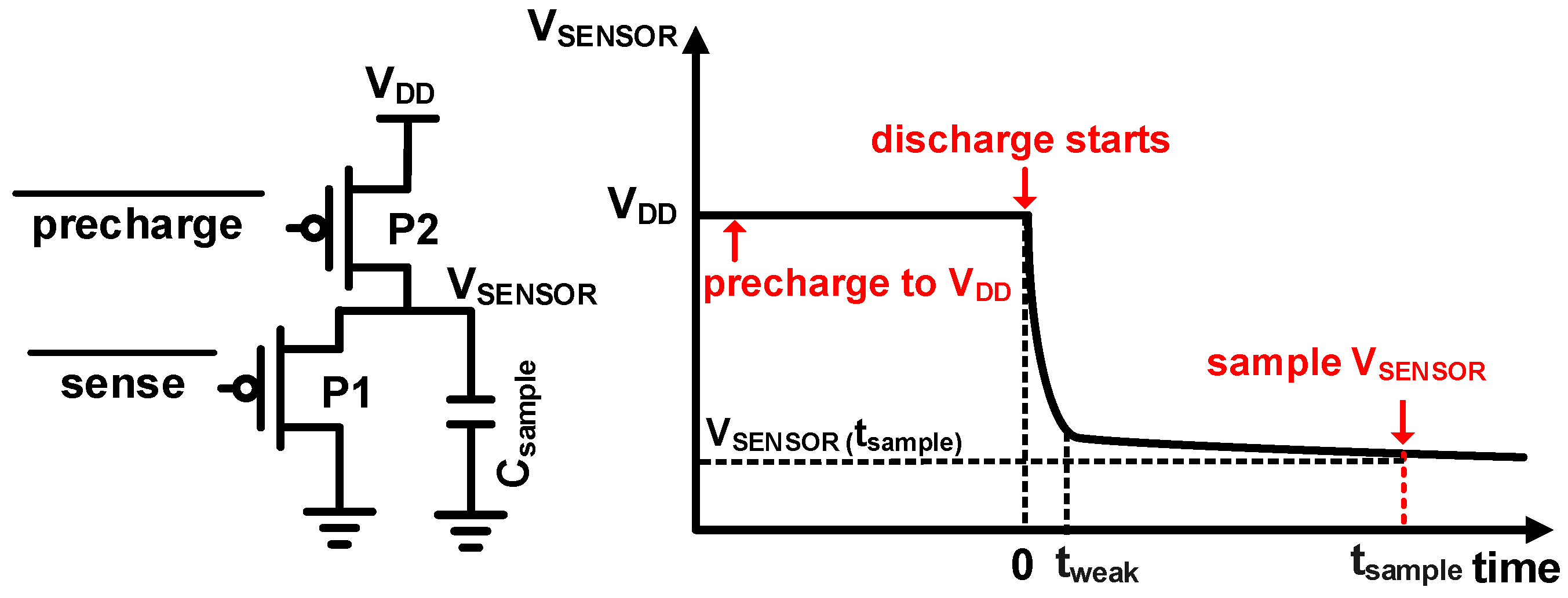
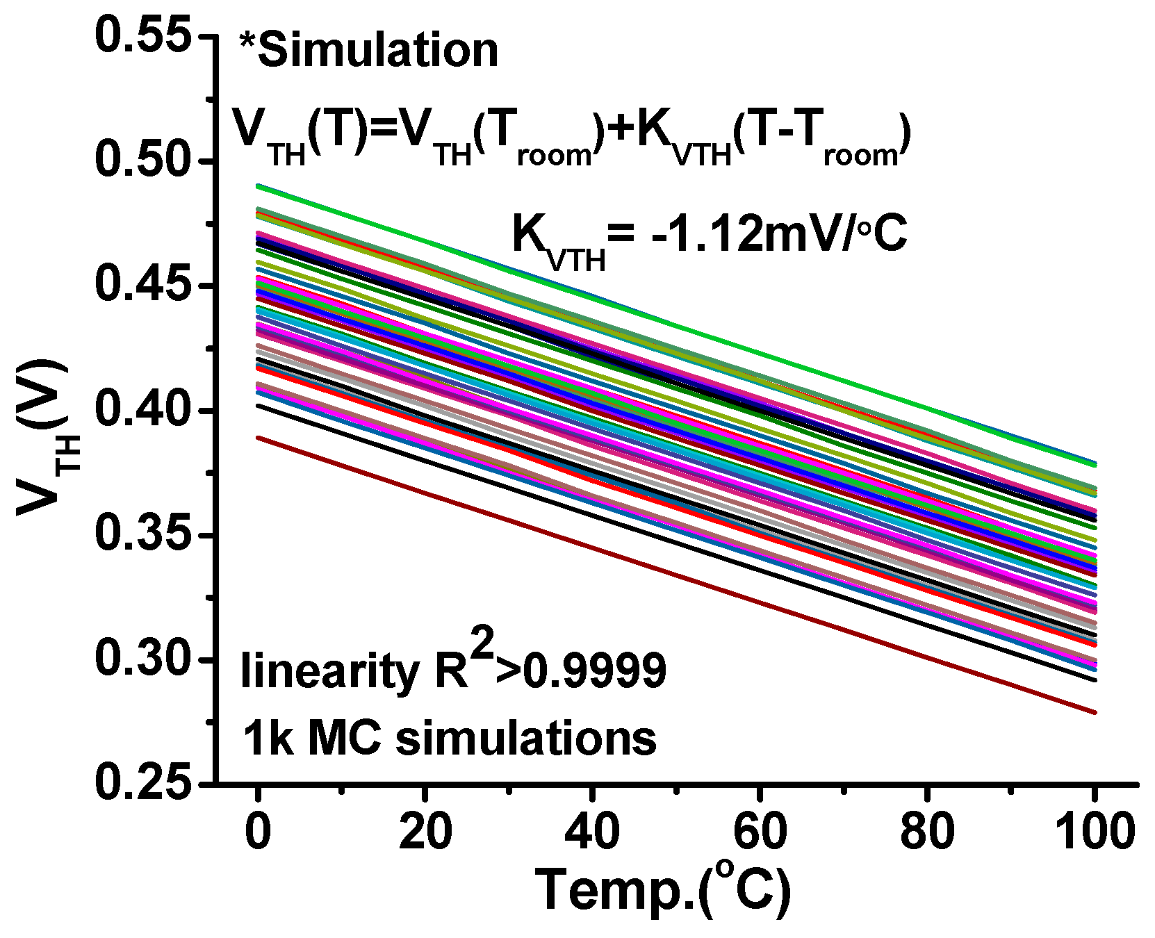
2.1. Operating Principle

The proposed frontend directly samples the VTH of a PMOS device P1 (Figure 2). VTH is well-known to have a strong and well-defined linear relationship with temperature and can be formulated as:
V TH ( T ) = V TH ( T room ) + K VTH · ( T T room )
where T is temperature, Troom is 300 K, and KVTH is the first-order temperature coefficient (TC) of VTH [28]. This is also confirmed with our SPICE simulation results showing a high linearity of R2 > 0.9999 and strong temperature coefficient (KVTH) of −1.12 mV/°C across process corner variation (Figure 3). The manufacturing process variation mostly modulates the offset of VTH curves and makes little impact on KVTH. This characteristic is well-suited for OPC.
To capture the VTH of P1, we propose to use the discharging behavior of a PMOS device, also known as VTH drop. This can be simply done by pre-charging the source voltage of P1 (VSENSOR in Figure 2), followed by discharging operation. Specifically, as shown in the waveform of Figure 2, we first use the shared pre-charging device P2 to pre-charge the shared sampling capacitor Csample (VSENSOR node) to VDD. Once the node is fully charged, we turn off P2 and turn on our sensing device P1 at time = 0 (in Figure 2). The P1 device starts to discharge VSENSOR node rapidly as it is initially in the strong-inversion region. At time = tweak, P1 gradually enters the weak-inversion region, and the discharging rate of VSENSOR node is largely reduced. This is known as the VTH drop phenomenon. Finally, we sample the voltage of VSENSOR node at the optimal sampling time (tsample).

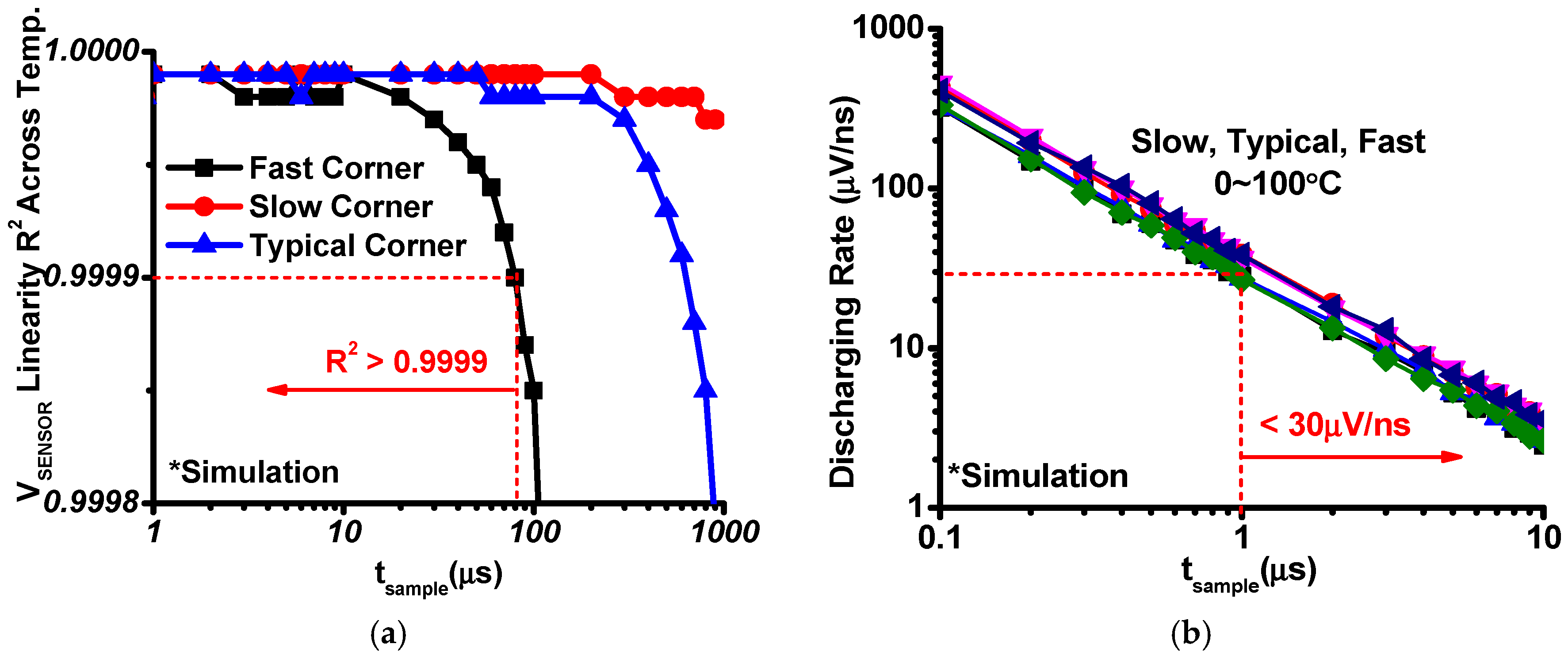
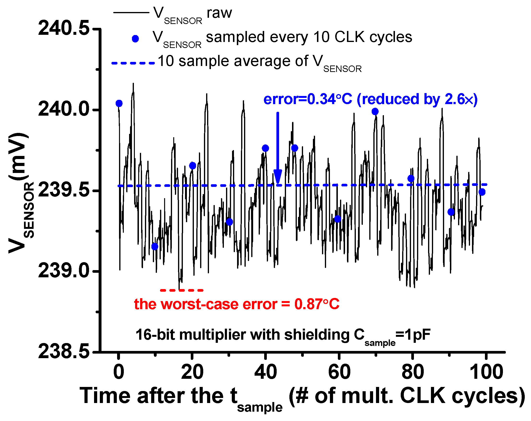
2.2. Optimal tsample

In the proposed sensor design, it is important to sample VSENSOR node at the optimal sampling time (tsample). This provides mainly four benefits, namely (i) good linearity of sampled VSENSOR values over temperature, (ii) robustness against leakage current of P1, (iii) robustness of TC of VSENSOR values against process variations, and (iv) robustness against pre-charged level (i.e., VDD) variations.
The optimal sampling time can be determined based on the two constraints that set the upper and lower bound. The upper bound is set by the leakage current of P1, which perturbs the desired sampled VSENSOR value. Intuitively, if we sample too late, the leakage current of P1 will modulate the VSENSOR value away from the VTH value of P1. In such case, the sampled VSENSOR value can be determined by VTH of P1 and will also be impacted by the leakage current of P1. Since leakage current has an exponential relationship with VTH of P1 (or temperature), the linearity of sampled VSENSOR over temperature can be deteriorated.
On the other hand, the lower bound is set by the fact that we need to wait until P1 surely enters weak inversion. In the boundary between strong and weak inversion, the discharging rate of VSENSOR node is relatively high and sampling time variation can largely degrade the accuracy of the sensor.
We perform circuit simulation to find the optimal range of sampling time. As expected, the linearity of sampled VSENSOR values rapidly degrades due to leakage when sampled too late (Figure 4a). To maintain the linearity R2 > 0.9999 across worst-case process corners, we set the upper bound of tsample to 80 µs. On the other hand, the discharging rate exponentially increases if tsample is too small (Figure 4b). A tsample that is larger than 1 µs can significantly reduce the discharging rate to <30 µV/ns since P1 is surely in weaker inversion. These set the optimal sampling time window to be between 1 µs to 80 µs after P1 is turned on. In modern IC technology, this range of time window is easy to locate since system clock has a much finer resolution.
Furthermore, we analytically confirm the validity of our intuition and simulation results on the optimal tsample. To understand the dependency of sampled VSENSOR values on temperature just after P1 enters weak inversion, we derive its equation to
V SENSOR ( t sample ) = V TH     I weak · ( t sample     t weak ) C sample
In Equation (2), tsample which is the moment to sample the VSENSOR node is more than 10× larger than tweak which is the time when P1 enters weak inversion region (e.g., tweak = 100 ns, tsample = 1 µs to 80 µs in the optimal sampling time window). Therefore, tweak can be ignored. Iweak, which is the sub-threshold leakage current of P1 when it just enters weak inversion region can be formulated as
I weak µ 0 · ( T T room ) K u · C OX · W L · ( n 1 ) · ( KT q ) 2 · exp ( V GS V TH ( T ) nV T ) µ 0 · C OX · W L · ( n 1 ) · ( K q ) 2 · T room K u · T K 0
µ 0 · C OX · W L · ( n 1 ) · ( K q ) 2 · T room K u + K 0 · ( 1 + T     T room T room ) K 0 µ 0 · C OX · W L · ( n 1 ) · ( K q ) 2 · T room K u + K 0 · ( 1 + K 0 · T T room T room )
µ 0 · C OX · W L · ( n 1 ) · ( K q ) 2 · T room K u + K 0 · [ ( 1 K 0 ) + K 0 T room · T ]
where Ku is the TC of the mobility (µ) and K0 = −Ku + 2. A key point in the derivation is that VGS is close to VTH(T) and thus the exponential term in Equation (3a) becomes 1. In addition, another high-order temperature dependent term, 1 +   T T room T room in Equation (3b), can be approximated to a linear function via the Taylor series since T T room T room is much smaller than 1 for the temperature range of interest. For example, for temperature range of 0 °C to 100 °C, this term is in the range of −0.09 and 0.24. Therefore, as shown in Equation (3c), Iweak also becomes a linear function of temperature. After plugging Equation (3c) and Equations (1) and (2), the value of VSENSOR node sampled at tsample can be formulated as
V SENSOR ( t sample ) ( V TH ( T room ) K VTH · T room A weak · t sample C sample ) + ( K VTH K weak · t sample C sample ) · T
where A weak = C · ( 1 K 0 )   and   K weak = C · K 0 T room , where   C = µ 0 · C OX · W L · ( n 1 ) · ( K q ) 2 · T room K u + K 0 .
The sampled VSENSOR value is a linear combination of the two parameters, VTH and Iweak, which are linear to temperature, and thus is also linear to temperature. If VSENSOR node is sampled after the optimal window, the assumption that VGS is close to VTH(T) used in deriving Equation (3a) becomes invalid, and thus the exponential term cannot be eliminated. This makes the sampled VSENSOR value exhibit poor linearity which matches our simulation results shown in Figure 4a.
From the above analytical study, we can find another important consideration on choosing the optimal tsample value. As shown in Equation (4), the TC of the sampled VSENSOR values is formulated as K VTH K weak · t sample C sample . In simulation, we saw that KVTH is well-maintained across process variation (Figure 3). However, the capacitance value of sampling capacitor (Csample) can have large variation across the process (e.g., Metal-Insulator-Metal capacitors have ~15% 3σ/µ variation). Also, Kweak value can also vary across the process variation depending on P1 sizing (i.e., W, L). Therefore, it is critical to minimize the impact of Csample and Kweak variation, which can be achieved by using the smallest allowable tsample value. We use tsample = 10 µs, so that KVTH (−1.12 mV/°C) can be more than 50× larger than the K weak · t sample C sample term.

2.3. Pre-Charge Level Variation

The optimal tsample also makes the proposed sensor robust against pre-charge level variation incurred by VDD noise. After the sensing device P1 turns on, if the pre-charge level varies, it can change tweak, i.e., the time P1 enters the weak inversion region. However, as shown in Equation (2), the tweak (100 ns) is two orders of magnitude smaller than optimal tsample (10 µs). Therefore, the tweak variation makes minimal impact on the accuracy. As shown in Figure 5, the simulation results show that the pre-charge level variation of 100 mV causes a negligible error increase of <0.02 °C. For the same reason, VTH offset variation due to process variation (i.e., VTH(Troom) in Equation (1)) also has a negligible impact on accuracy. The VTH(Troom) variation only affects the offset of the sampled VSENSOR value in Equation (4) and can be calibrated out via OPC. As a result, process variation also has a negligible impact on the optimal tsample found in Section 2.2.

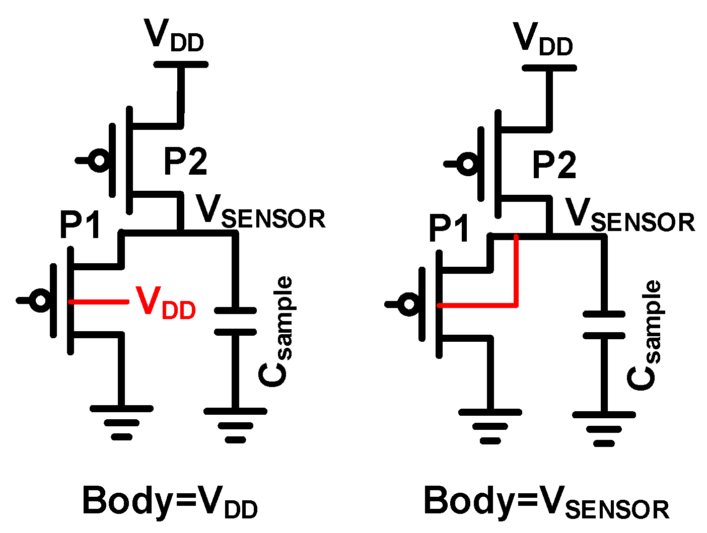
2.4. Sensor Device Type and Body Connection

We explore various device types provided in the 65 nm process for the proposed sensor frontend. We simulate the accuracy by running 100 Monte-Carlo simulations with process variation and performing OPC. In the simulation, we compare 2.5 V thick-oxide device and 1 V thin-oxide device with different VTHs (i.e., high-VTH, standard-VTH, and low-VTH). We choose the optimal sensor size and tsample value for each device types while sweeping the length by 1–10× of the minimum, width by 1–30× of the minimum, and the tsample value from 1 µs to 100 µs. For all the device types, the sample capacitor (Csample) value is fixed to 1 pF. The results are summarized in Table 1. All the device types achieve the 3σ-error of <2.72 °C while the 2.5 V thick-oxide device achieves the best 3σ-error of 0.93 °C.
We also simulate the sensor circuits using 2.5 V thick-oxide devices across two different body connections, i.e., connected to VDD or VSENSOR (Figure 6). As shown in Table 2, the sensor with body connected to VDD achieved better accuracy. However, if VDD is susceptible to large noise, the body can be connected to VSENSOR or a separate clean bias voltage with <0.06 °C nominal accuracy degradation.

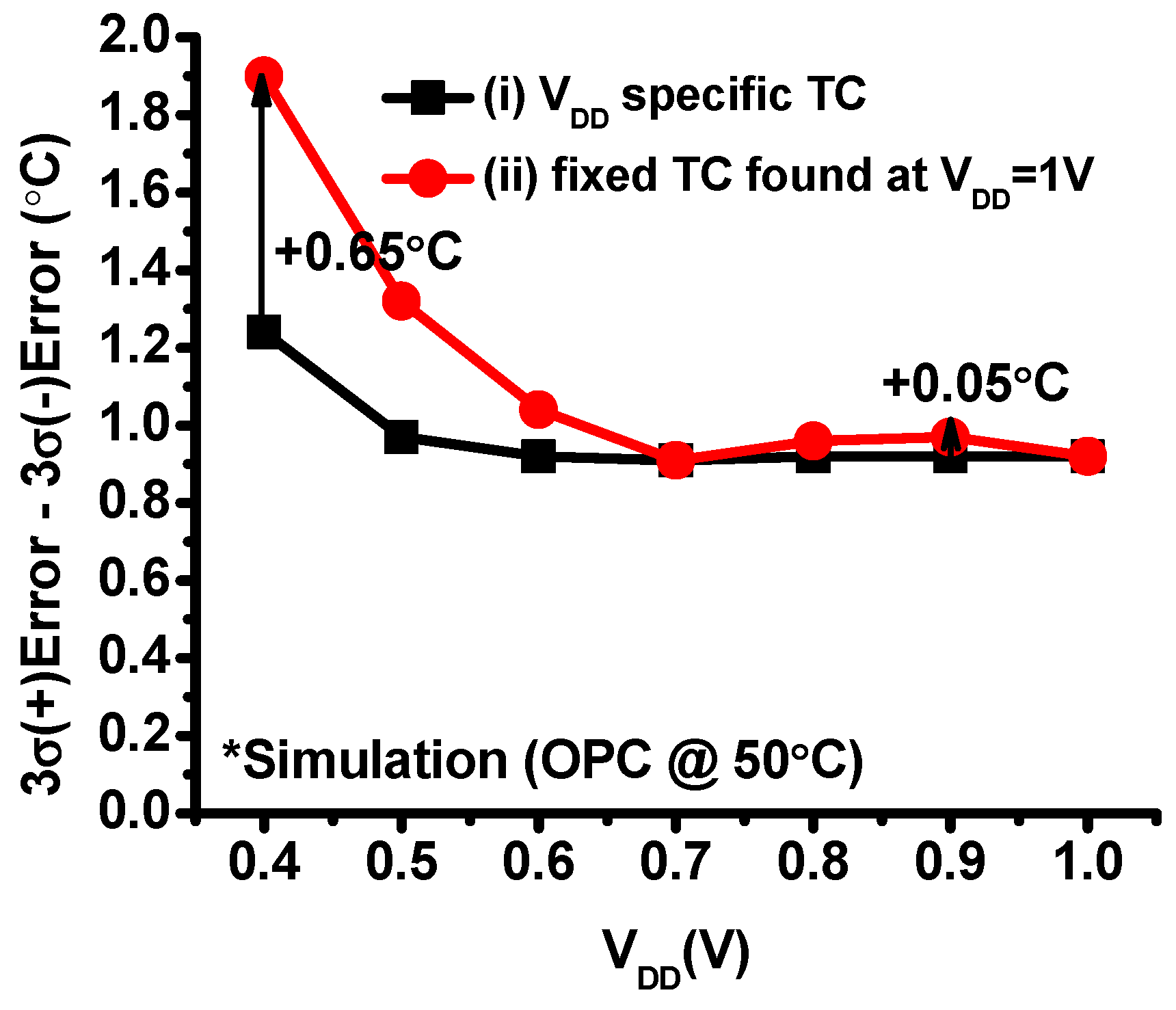
2.5. VDD Scalability and Noise

We experiment voltage scalability of the proposed frontends. To evaluate this, we simulate the 3σ-error of the sensor frontend whose body is connected to VDD. We perform OPC and calculate the accuracy across 0.4 to 1 V using (i) VDD specific TC and (ii) the fixed TC found at VDD = 1 V. Using the single TC found at 1 V, the downscaling to 0.4 V incurs additional 0.98 °C error for the 3σ case. If VDD specific TCs are used, the additional error is reduced to 0.33 °C. Using VDD specific TCs achieves better accuracy. However, it requires to add a lookup table storing those TC values in the DVS/UDVS control systems.
One of the challenges in the remote sensing approach is VDD noise. If the body of our frontend (P1) is connected to VDD, VDD change during the tsample period could affect the output voltage. The result of the second case (the fixed TC) shows that even with 100 mV VDD variation during the tsample period, the accuracy is only degraded by 0.05 °C (Figure 7). Another potential concern for the remote thermal sensing approach is substrate noise in the hotpot location since hotspots are likely to have higher switching activity and thereby have more substrate noise. However, the proposed sensor does not have any direct connection to substrate and thus mostly immune from substrate noise.

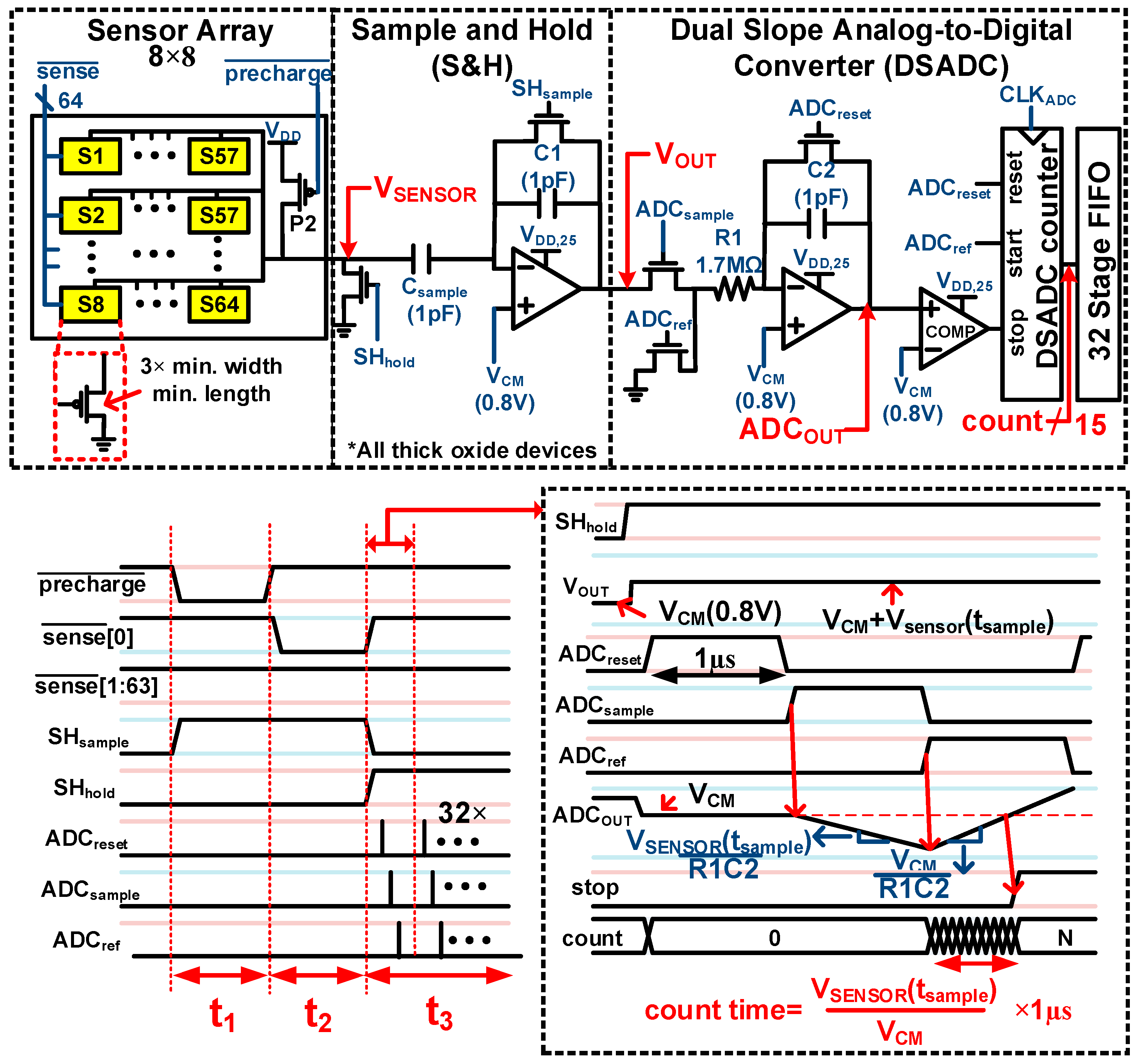
3. Test Chip Details

The test chip is designed and fabricated in a 65 nm general-purpose CMOS process. Figure 8 shows the die photo of the test chip. The test chip consists of (i) an 8 × 8 frontends, each frontend being able to be configured from Sensor-Size-1 to Sensor-Size-64 (SS1 to SS64); (ii) shared sample and hold circuits (S&H); and (iii) on-chip read-out circuitry using the dual-slope analog-to-digital converter (DSADC) topology (Figure 9). We assume those are a part of the remote sensing architecture. Each unit-size sensor is a 3× minimum-sized 2.5 V thick-oxide PMOS device with its body tied to VDD. We used this device and configuration since it achieves the best accuracy as discussed in Section 2.4. The reference voltage (VCM) for the S&H and DSADC can be generated by e.g., an accurate bandgap voltage reference (not included in this test chip). Such bandgap circuits may require vertical BJT devices, limiting area and voltage scalability. However, as the voltage reference is shared by multiple frontends, its overhead can be amortized. Also, in the remote sensing architecture, the backend circuitries including the voltage reference are placed in a location away from main digital circuits, which can relax its requirement on area and voltage scalability. We implement a 1 pF capacitor for Csample. Further investigation on the different sizes for Csample will be presented in Section 5.

3.1. P2 and Csample Sharing

The pre-charge PMOS device (P2), the sampling capacitor (Csample), and the S&H are shared by multiple frontends, providing mainly three benefits. First, each frontend sees the identical load capacitance which is the sum of Csample and the capacitance of all wires connecting Csample and the frontends. This makes the TC of sampled VSENSOR value (i.e., K VTH K weak · t sample C sample ) to be the same. Second, the manufacturing variation of Csample makes little impact on accuracy since each frontend sees the same variation, which then is calibrated out by OPC. Last but not the least, the sharing can save the area.
When a frontend is sensing, all the other sensors receive VDD on their gates. This forms negative VGS in the frontends and suppresses the leakage of the inactive sensors. Also, if no temperature sensing is requested, all frontends receive VDD. This helps prevent aging effects such as NBTI from degrading the long-term accuracy of frontends.

3.2. Operating Principle

The operational waveform of a test chip is shown in Figure 9. During period t1, the VSENSOR node is pre-charged to VDD by P2. Then, during period t2 (which is our tsample), P2 is turned off, and one of the selected sensor is turned on and discharges the VSENSOR node. During this t1 + t2 period, the S&H is in the sampling mode. At last, during period t3, S&H captures the VSENSOR value on VOUT and enters hold mode. The VOUT value which is the sum of VCM (=0.8 V) and VSENSOR at the time tsample is digitized by an off-chip ADC (16 bit, ±5 V) or by on-chip DSADC.

3.3. On-Chip DSADC

We design an on-chip DSADC to digitize VOUT 32 times and store them in the digital memory (FIFO) (Figure 9). The average of the 32 values is used for the temperature measurement. The DSADC digitization process is as follows. First, ADCOUT resets to VCM for 1 μs. The DSADC counter also resets to zero. Second, ADCOUT is discharged for a fixed period of 1 μs at the rate of VSENSOR(tsample)/R1C2. Third, the DSADC counter starts, and ADCOUT is charged with a fixed rate of VCM/R1C2. In the course of charging, the comparator finds the moment when the ADCOUT becomes larger than VCM and stops the counter. The digital counter output (count), which is formulated as VSENSOR(tsample) × 1 μs/VCM, represents the temperature that the sensor core measures. The counter operates at 1.5GHz with a resolution of 0.5 °C/count.

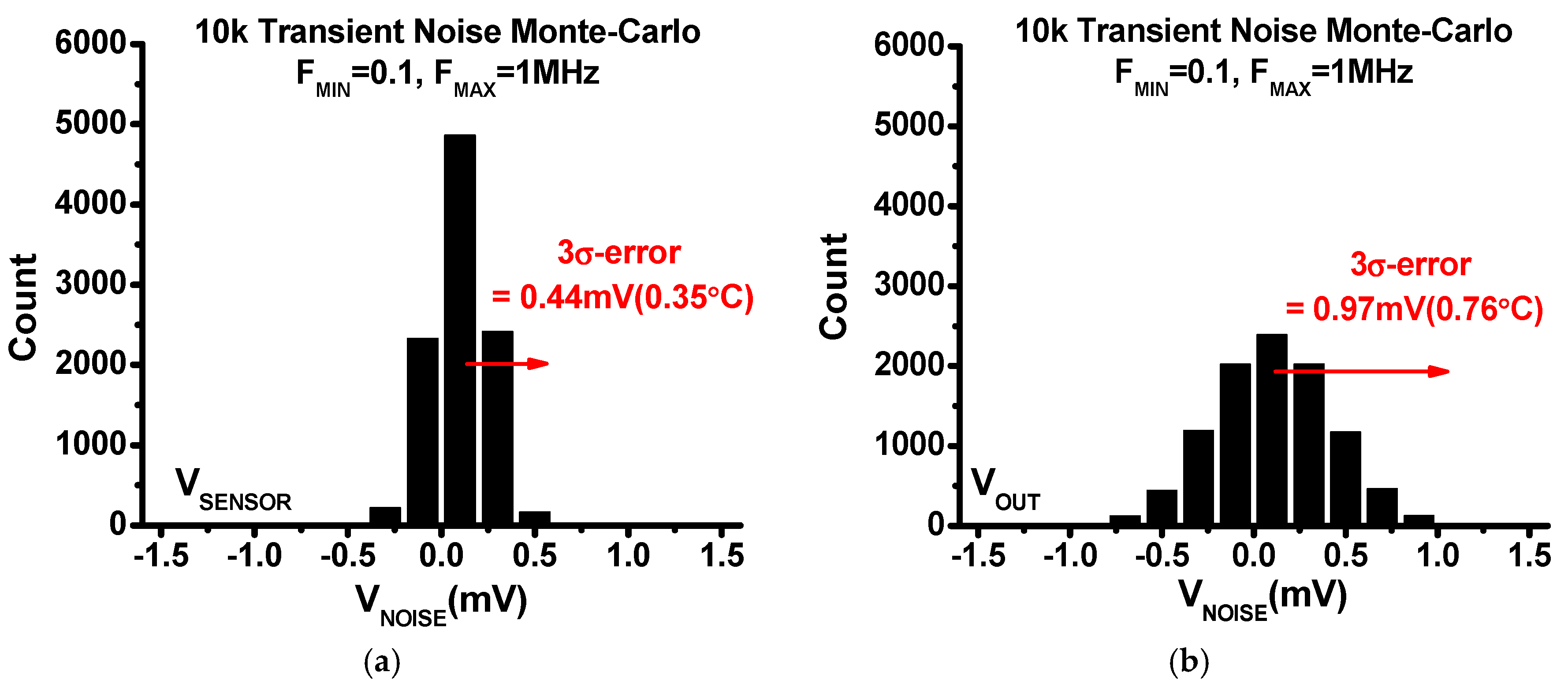
3.4. Noise Simulation

The impact of flicker and thermal noise on the accuracy of the proposed frontend is investigated using the transient noise analysis methodology outlined in [29]. Specifically, 10 k Monte-Carlo simulation with transient noise analyses is performed, and noise statistics is gathered. The FMIN and FMAX is set to 0.1 Hz and 1 MHz, respectively. In this simulation, the noise on the two output nodes VSENSOR and VOUT (Figure 9) is examined (Figure 10). The 3σ voltage noise (VNOISE) on node VSENSOR is 0.44 mV, translated to 0.35 °C error. The 3σ VNOISE on VOUT is 0.97 mV (=0.76 °C).

4. Measurement Results

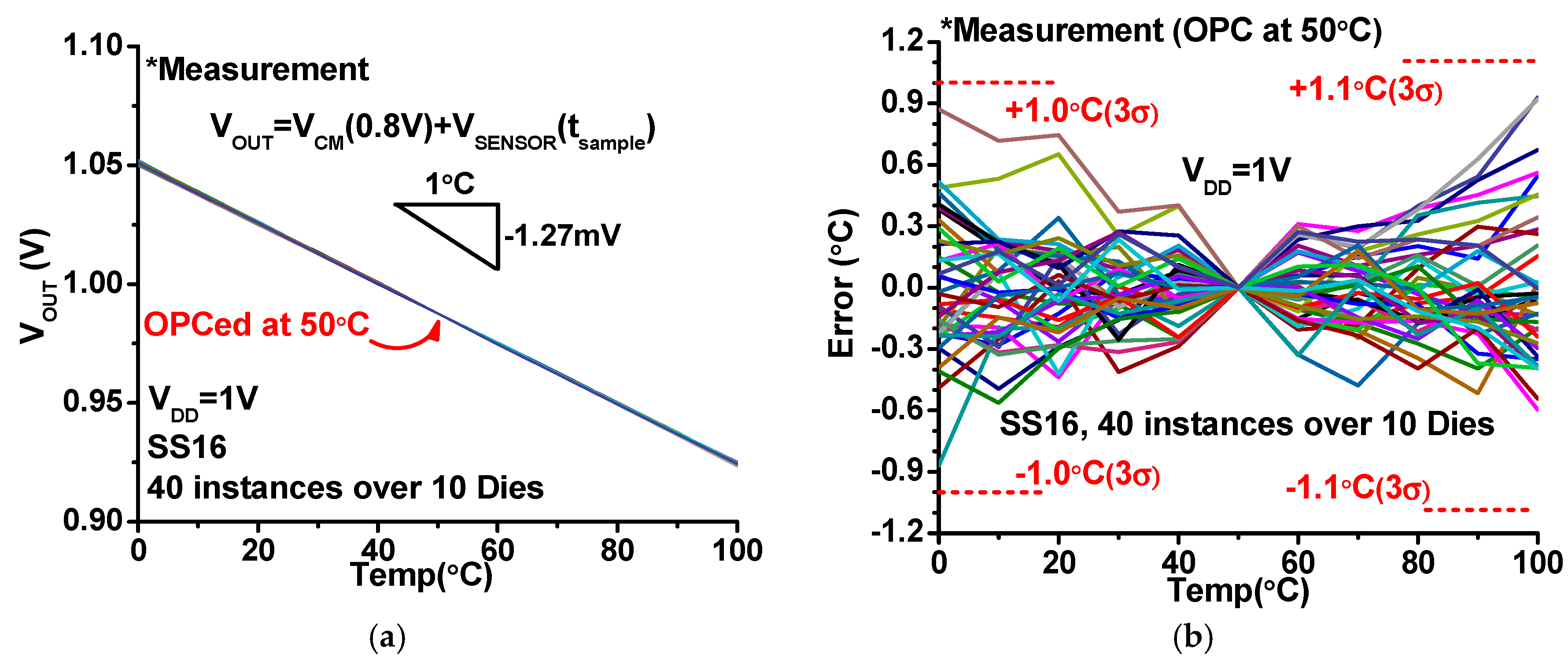
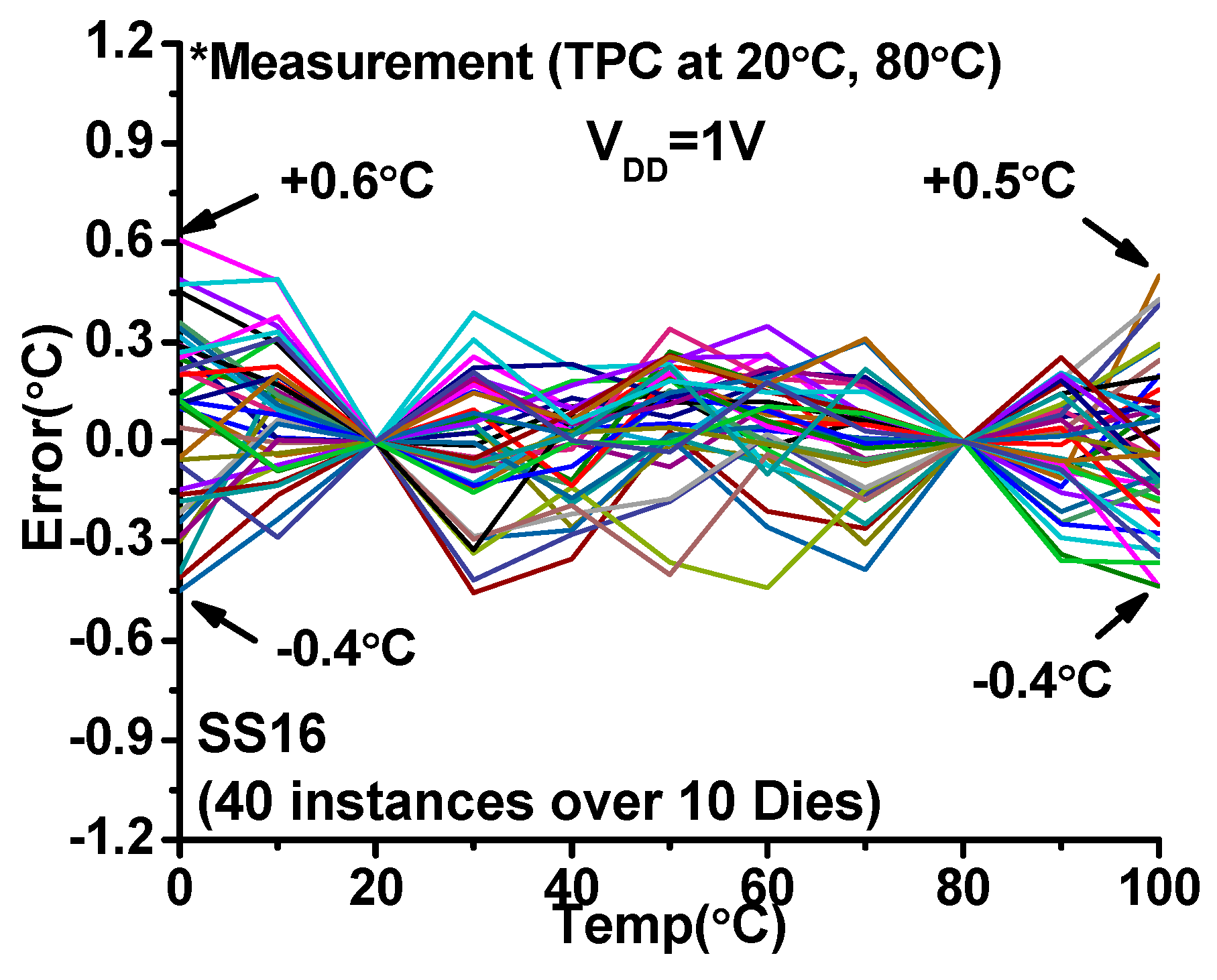
4.1. Sensor Accuracy Measurement

Each of the randomly chosen 10 test chips is placed in a temperature chamber and measured while the temperature is swept from 0 °C to 100 °C with 10 °C steps. We measure the sensors across 10 dies (total 40 SS16 frontends) using off-chip ADC (±5 V, 16b in a National Instruments data-acquisition PCI card) and the on-chip DSADC. The sensor reading is calibrated with OPC at 50 °C and the error is calculated using a fixed TC for all the sensors in 10 dies. In all the measurement, the t1 and t2 in Figure 9 are set to be 1 µs and 10 µs, respectively. Therefore, the raw sampling rate is 91 kS/s.
To study the impact of sensor area on accuracy, multiple unit-size sensors are combined and measured with the off-chip ADC. As more unit-size sensors are combined to form a larger sensor, the accuracy is improved (Figure 11). When 16 of unit-size sensors are combined (i.e., SS16), it achieves the 3σ-error of ±1.1 °C post OPC. The footprint is 30.1 µm2. The VOUTs of the 40 SS16 sensors after OPC is shown in Figure 12a. The average TC is measured to be −1.27 mV/°C. The measured error is shown in Figure 12b. We also perform two temperature point calibration (TPC) at 20 °C and 80 °C (Figure 13). The TPC can further reduce error down to −0.4 °C/+0.6 °C.
We also investigate the impact of tsample on accuracy (Figure 14). As expected from discussion in Section 2.2, the worst-case error (i.e., max.(+)error–max.(−)error) exhibits a bathtub-shape curve with an optimal tsample appearing between 1µs and 100µs, which achieves the worst-case error of less than 2 °C.

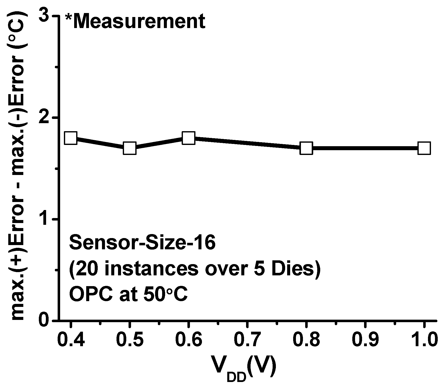
4.2. Supply Voltage Scalability Measurement

We also measure VDD scalability of the sensors (Figure 15). The same measurement methodology described in Section 4.1 is used for the SS16 frontends except VDD is swept from 0.4 V to 1 V. The measurements across 20 instances across 5 chips show that the worst-case errors are found nearly constant, around 1.8 °C across VDDs.

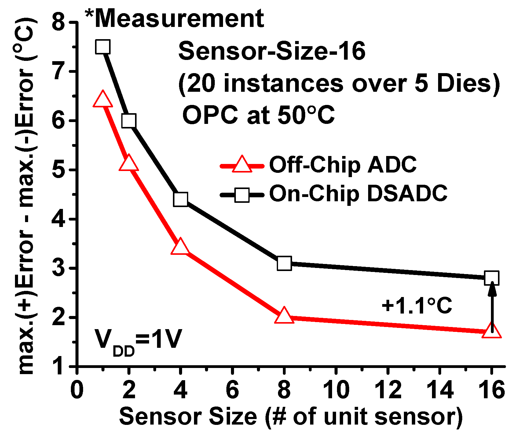
4.3. On-Chip DSADC Measurement

We repeat the measurement in Section 4.1 using on-chip DSADC (Figure 16). The measurement across 5 chips shows the worst-case error increase by 1.1 °C, as compared to the measurement using the off-chip ADC. The increased error is mainly due to the resolution limitation (0.5 °C) of the DSADC.

4.4. Comparisons

As summarized in Table 3, the proposed frontend is compared to the previous temperature sensor works. The proposed sensor frontend has 30.1 µm2 area and <±1.1 °C 3σ-error across 40 instances in 10 dies. As shown in Figure 1, the proposed frontend significantly advances the existing area and accuracy trade-off among the MOSFET based designs: the proposed sensor achieves 9× smaller area and 3× higher accuracy than the previous smallest design [15]. The proposed sensor frontend also achieves the voltage scalability down to 0.4 V, which is 50 mV lower than [16], while achieving 35× smaller area and 1.4× higher accuracy.

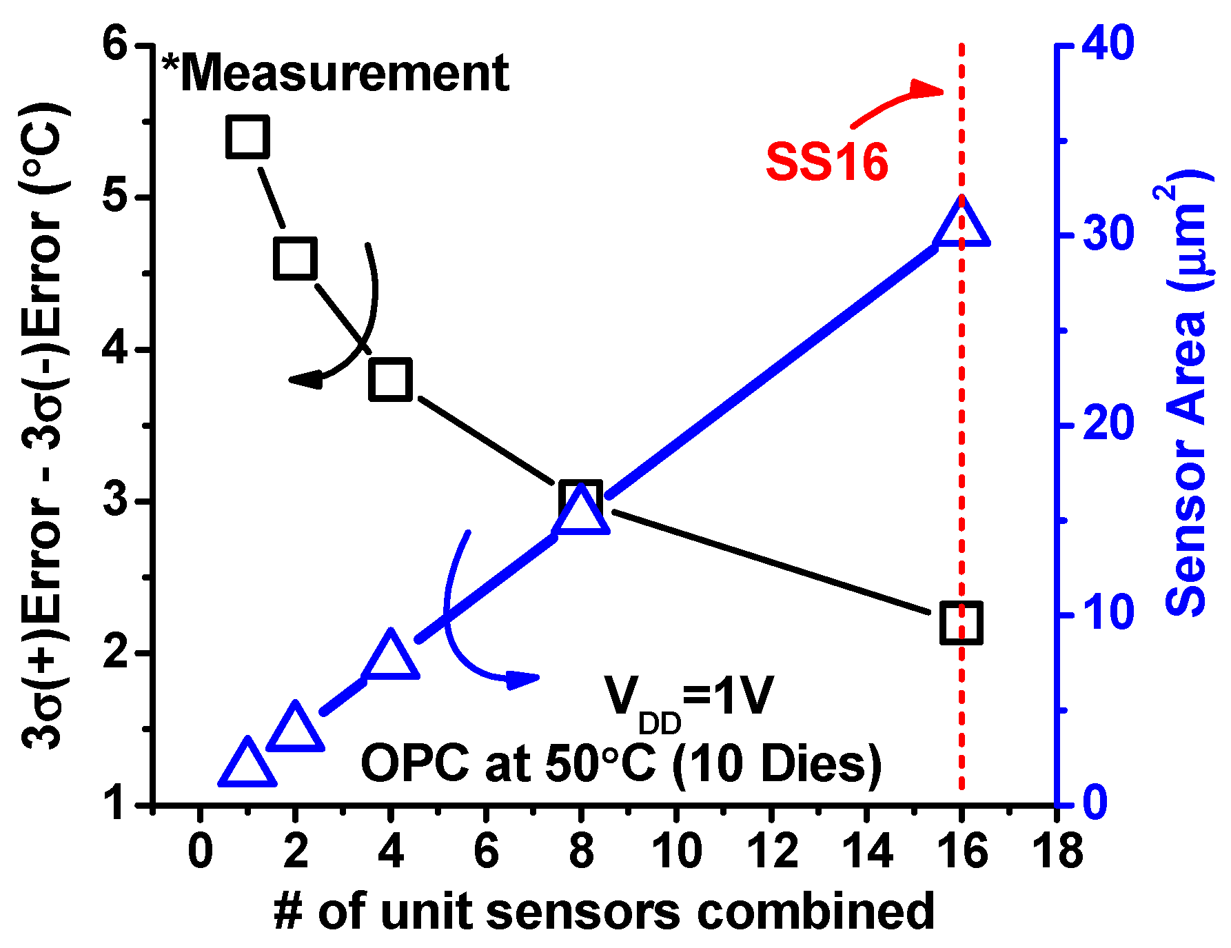
5. Digital Standard-Cell-Compatible Sensor Experiment

In this section, we investigate the placement of our proposed frontend in digital circuits that are designed and laid out in the automatic standard cell design flow. First, we layout the proposed SS16 frontend in the same digital standard-cell format. This takes the area of 3.6 × 9.2 = 33.12 µm2 (Figure 17). Then, we use a commercial place and route tool and place one frontend in the center of the multiplier circuits. We use four different-size multipliers, each having the input data widths of 8, 16, 32, or 64 bits. All the multipliers are synthesized with the standard cells using 1V thin-oxide standard-VTH devices.
We study the impact of coupling noise of digital circuits on the sensor output (VSENSOR) using the SPICE simulation with the parasitic-extracted netlists and VDD = 1 V. Specifically, we simulate the VSENSOR node while the multiplier actively switches. To extract the inaccuracy only incurred by digital noise, we run two simulations with and without multiplier switching activities and take the difference between them. We also take 1000 samples across varying input vectors for 100 multiplier-clock (CLK) cycles. Figure 18a shows the worst-case coupling noise found in the simulation. It shows that the coupling-induced error increases with larger multipliers since the wire of the VSENSOR node becomes longer and thus exposed to more of digital circuits.
One technique to reduce coupling noise is to shield the sensitive node with stable voltage (e.g., VDD or VSS). For example, as shown in Figure 18a, shielding the VSENSOR node with VSS reduces the worst-case error by ~2× in the 64-bit multiplier.
Another technique is to use a larger sampling capacitor. This increases the capacitance of a victim wire relative to coupling capacitance. As shown in Figure 18b, larger sampling capacitors proportionally reduce the worst-case error. For example, in the experiment with the 64-bit multiplier and the VSENSOR node being shielded, 10× larger sampling capacitor (i.e., 10 pF) reduces the worst-case error proportionally by 10× to 0.44 °C (the 1 pF sampling capacitor can incur the worst-case error of 4.04 °C). Large sampling capacitors, however, can increase backend area, reduce sampling speed (see Section 4 for details) and increase energy dissipation per sampling.
Finally, we study the last technique—averaging—to mitigate coupling noise impact. Figure 19 shows the VSENSOR node voltage while the multiplier is computing random input vectors at every CLK cycle. We sample the VSENSOR node multiple times uniformly (every 10 CLK cycle) after an optimal tsample, and then we average 10 samples. The results show that the averaging technique can reduce coupling induced error by 2.6× as compared to the worst case. To implement the averaging operation, we can use the local FIFO in the on-chip DSADC (discussed in Section 3.3)
In larger designs, the impact of coupling noise on sensor accuracy can become significant. Also, as the metal wire network connecting frontends becomes larger, the resistance and capacitance of the metal wire can make more prominent impact on delay and sensor accuracy. To mitigate these problems, one can consider hierarchical networks which disable the unused part of networks, and potentially have multiple backends [8,16,17].

6. Conclusions

In this paper, we propose a temperature sensor frontend based on a novel mechanism of direct VTH sensing. The proposed frontend achieves compact footprint (30.1 µm2), low 3σ-error (±1.1 °C; across 0 to 100 °C; after OPC), and good voltage scalability (1 to 0.4 V) without losing much accuracy. This is 9× smaller and 3× more accurate than the prior art [15]. It also operates at 50 mV lower than the prior art while achieving while achieving 35× smaller area and 1.4× higher accuracy [16]. The proposed sensor frontend is in the scale of a digital standard cell, which enables an aggressive sensor placement, virtually on a target hotspot. The proposed sensor can enable accurate dense thermal monitoring in modern VLSI systems.

Author Contributions

S.K. is the main author of the paper. M.S. was responsible for supervising the paper.

Acknowledgments

This research is supported in part by the Catalyst Foundation, DARPA MTO PERFECT Program (C#: HR0011-13-C-0003), and an NSF CAREER Award.

Conflicts of Interest

The authors declare no conflict of interest.

References

  1. Long, J.; Memik, S.O.; Memik, G. Thermal Monitoring Mechanisms for Chip Multiprocessors. ACM Trans. Archit. Code Optim. 2008, 5, 9. [Google Scholar] [CrossRef]
  2. Nowroz, A.N.; Cochran, R.; Reda, S. Thermal Monitoring of Real Processors: Techniques for Sensor Allocation and Full Characterization. In Proceedings of the 2010 47th ACM/IEEE Design Automation Conference, Anaheim, CA, USA, 13–18 June 2010; pp. 56–61. [Google Scholar]
  3. Chundi, P.K.; Zhou, Y.; Kim, M.; Kursun, E.; Seok, M. Evaluation of Miniature Temperature Sensors on On-Chip Hotspot Monitoring. In Proceedings of the ACM/IEEE International Symposium on Low Power Electronics and Design (ISLPED), Taipei, Taiwan, 24–26 July 2017. [Google Scholar]
  4. Souri, K.; Makinawa, K. A 0.12 mm2 7.4 µW Micropower Temperature Sensor with an Inaccuracy of ±0.2 °C (3σ) from −30 °C to 125 °C. IEEE J. Solid-State Circuits 2011, 46, 1693–1700. [Google Scholar] [CrossRef]
  5. Souri, K.; Chae, Y.; Makinawa, K. A CMOS Temperature Sensor with a Voltage-Calibrated Inaccuracy of ±0.15 °C (3σ) from −55 °C to 125 °C. IEEE J. Solid-State Circuits 2013, 48, 292–301. [Google Scholar] [CrossRef]
  6. Shor, J.S.; Luria, K. Miniaturized BJT-Based Thermal Sensor for Microprocessors in 32- and 22-nm Technologies. IEEE J. Solid-State Circuits 2013, 48, 2860–2867. [Google Scholar] [CrossRef]
  7. Oshita, T.; Shor, J.; Duarte, D.E.; Kornfeld, A.; Zilberman, D. Compact BJT-Based Thermal Sensor for Processor Applications in a 14 nm tri-Gate CMOS Process. IEEE J. Solid-State Circuits 2015, 50, 799–807. [Google Scholar] [CrossRef]
  8. Lakdawala, H.; Li, Y.W.; Raychowdhury, A.; Taylor, G.; Soumyanath, K. A 1.05 V 1.6 mW, 0.45 °C 3σ Resolution ΔΣ Based Temperature Sensor with Parasitic Resistance Compensation in 32 nm Digital CMOS Process. IEEE J. Solid-State Circuits 2009, 44, 3621–3630. [Google Scholar] [CrossRef]
  9. Eberlein, M.; Yahav, I. A 28 nm CMOS Ultra-Compact Thermal Sensor in Current-Mode Technique. In Proceedings of the IEEE Symposium on VLSI Circuits, Honolulu, HI, USA, 15–17 June 2016; pp. 1–2. [Google Scholar]
  10. Saneyoshi, E.; Nose, K.; Kajita, M.; Mizuno, M. A 1.1 V 35 µm × 35 µm thermal sensor with supply voltage sensitivity of 2 °C/10%-supply for thermal management on the SX-9 supercomputer. In Proceedings of the IEEE Symposium on VLSI Circuits, Honolulu, HI, USA, 18–20 June 2008; pp. 152–153. [Google Scholar]
  11. Kim, K.; Lee, H.; Jung, S.; Kim, C. A 366 kS/s 400 uW 0.0013 mm2 Frequency-to-Digital Converter based CMOS temperature sensor using multiphase clock. In Proceedings of the IEEE Custom Integrated Circuits Conference, San Jose, CA, USA, 13–16 December 2009; pp. 203–206. [Google Scholar]
  12. Souri, K.; Chae, Y.; Thus, F.; Makinawa, K. A 0.85 V, 600 nW All-CMOS Temperature Sensor with an Inaccuracy of ±0.4 °C (3σ) from −40 °C to 125°C. In Proceedings of the 2014 IEEE International Solid-State Circuits Conference Digest of Technical Papers, San Francisco, CA, USA, 9–13 February 2014; pp. 222–223. [Google Scholar]
  13. Hwang, S.; Koo, J.; Kim, K.; Lee, H.; Kim, C. A 0.008 mm2 500 µW 469 kS/s Frequency-to-Digital Converter Based CMOS Temperature Sensor with Process Variation Compensation. IEEE Trans. Circuits Syst. I Regul. Pap. 2013, 60, 2241–2248. [Google Scholar] [CrossRef]
  14. Shim, D.; Jeong, H.; Lee, H.; Rhee, C.; Jeong, D.-K.; Kim, S. A Process-Variation-Tolerant On-Chip CMOS Thermometer for Auto Temperature Compensated Self-Refresh of Low-Power Mobile DRAM. IEEE J. Solid-State Circuits 2013, 48, 2550–2557. [Google Scholar] [CrossRef]
  15. Yang, T.; Kim, S.; Kinget, P.R.; Seok, M. Compact and Supply-Voltage-Scalable Temperature Sensors for Dense On-Chip Thermal Monitoring. IEEE J. Solid-State Circuits 2015, 50, 2773–2785. [Google Scholar] [CrossRef]
  16. Lu, L.; Duarte, D.E.; Li, C. A 0.45 V MOSFETs-based Temperature Sensor Frontend in 90 nm CMOS With a Non-Calibrated ±3.5 °C 3σ Relative Inaccuracy from −55 °C to 105 °C. IEEE Trans. Circuits Syst. II Express Briefs 2013, 60, 771–775. [Google Scholar] [CrossRef]
  17. Lu, L.; Vosooghi, B.; Dai, L.; Li, C. A 0.7 V Relative Temperature Sensor with a Non-Calibrated ±1 °C 3σ Relative Inaccuracy. IEEE Trans. Circuits Syst. I Regul. Pap. 2015, 62, 2434–2444. [Google Scholar] [CrossRef]
  18. Saligane, M.; Khayatzadeh, M.; Zhang, Y.; Jeong, S.; Blaauw, D.; Sylvester, D. All-Digital SoC Thermal Sensor using On-Chip High Order Temperature Curvature Correction. In Proceedings of the IEEE Custom Integrated Circuits Conference, San Jose, CA, USA, 28–30 September 2015. [Google Scholar]
  19. Quan, R.; Sonmez, U.; Sebastiano, F.; Makinwa, K.A.A. A 4600 µm2 1.5 °C (3σ) 0.9 kS/s Thermal-Diffusivity Temperature Sensor with VCO-Based Readout. In Proceedings of the IEEE International Solid-State Circuits Conference Digest of Technical Papers, San Francisco, CA, USA, 22–26 February 2015; Volume 58, pp. 488–489. [Google Scholar]
  20. Sonmez, U.; Sebastiano, F.; Makinwa, K.A.A. 1650 µm2 Thermal-Diffusivity Sensors with Inaccuracies Down to ±0.75 °C in 40 nm CMOS. In Proceedings of the IEEE International Solid-State Circuits Conference Digest of Technical Papers, San Francisco, CA, USA, 31 January–4 February 2016; pp. 206–207. [Google Scholar]
  21. Dorsey, J.; Searles, S.; Ciraula, M.; Johnson, S.; Bujanos, N.; Wu, D.; Braganza, M.; Meyers, S.; Fang, S. An Integrated Quad-Core OpteronTM Processor. In Proceedings of the IEEE International Solid-State Circuits Conference Digest of Technical Papers, San Francisco, CA, USA, 11–15 February 2007; pp. 102–103. [Google Scholar]
  22. Floyd, M.; Allen-Ware, M.; Rajamani, K.; Brock, B.; Lefurgy, C.; Drake, A.J.; Bose, P.; Buyuktosunoglu, A. Introducing the adaptive energy management features of the power 7 chip. IEEE Micro 2011, 31, 60–75. [Google Scholar] [CrossRef]
  23. Fluhr, E.J.; Friedrich, J.; Dreps, D.; Zyuban, V.; Still, G.; Gonzalez, C.; Hall, A.; Hogenmiller, D.; Malgioflio, F.; Nett, R.; et al. 5.1 POWER8TM: A 12-core server-class processor in 22 nm SOI with 7.6 Tb/s off-chip bandwidth. In Proceedings of the 2014 IEEE International Solid-State Circuits Conference Digest of Technical Papers, San Francisco, CA, USA, 9–13 February 2014; pp. 96–97. [Google Scholar]
  24. Rangan, K.K.; Wei, G.; Brooks, D. Thread motion: Fine-grained power management for multi-core systems. In Proceedings of the 36th Annual International Symposium on Computer Architecture (ISCA), Austin, TX, USA, 20–24 June 2009; pp. 302–313. [Google Scholar]
  25. Truong, D.N.; Cheng, W.H.; Mohsenin, T.; Yu, Z.; Jacobson, A.T.; Landge, G.; Meeuwsen, M.J.; Watnik, C.; Tran, A.T.; Xiao, Z.; et al. A 167-processor computational platform in 65 nm CMOS. IEEE J. Solid-State Circuits 2009, 44, 1130–1144. [Google Scholar] [CrossRef]
  26. Makinwa, K.A.A. Temperature Sensor Performance Survey. TU Delft, The Netherlands. Available online: http://ei.ewi.tudelft.nl/docs/TSensor_survey.xls (accessed on 25 May 2018).
  27. Kim, S.; Seok, M. A 30.1 μm2, <±1.1 °C-3σ-Error, 0.4-to-1.0 V Temperature Sensor based on Direct Threshold-Voltage Sensing for On-Chip Dense Thermal Monitoring. In Proceedings of the 2015 IEEE Custom Integrated Circuits Conference, San Jose, CA, USA, 28–30 September 2015. [Google Scholar]
  28. Tsividis, Y.; McAndrew, C. Operation and Modeling of the MOS Transistors, 3rd ed.; Oxford University Press: Oxford, UK, 2011. [Google Scholar]
  29. Murmann, B. Thermal Noise in Track-and-Hold Circuits: Analysis and Simulation Techniques. IEEE Solid-State Circuits Mag. 2012, 4, 46–54. [Google Scholar] [CrossRef]
Figure 1. Area, error, and VDD,min comparisons of recent compact thermal sensors.
Jlpea 08 00016 g001
Figure 2. Schematic and operation of the proposed sensor frontend that directly samples VTH.
Jlpea 08 00016 g002
Figure 3. VTH over temperature across process corner variations.
Jlpea 08 00016 g003
Figure 4. (a) Linearity of the sampled VSENSOR values across tsample; (b) Discharging rate of the VSENSOR node voltage across tsample.
Jlpea 08 00016 g004
Figure 5. Impact of the pre-charge level (VDD) variation on accuracy.
Jlpea 08 00016 g005
Figure 6. Two different possible body connections of the sensing device P1.
Jlpea 08 00016 g006
Figure 7. Simulated accuracy across supply voltage where OPC is performed with (i) VDD specific TCs and (ii) the fixed TC found at 1 V.
Jlpea 08 00016 g007
Figure 8. Die photo.
Jlpea 08 00016 g008
Figure 9. Test chip block diagram and its operational waveform.
Jlpea 08 00016 g009
Figure 10. Simulated voltage noise histogram from Monte-Carlo based transient noise simulation on (a) the node VSENSOR and (b) the node VOUT.
Jlpea 08 00016 g010
Figure 11. Accuracy and area trade-off across sensor sizes.
Jlpea 08 00016 g011
Figure 12. (a) Measured VOUTs of SS16 after one temperature point calibration (OPC) at 50 °C; (b) Errors across temperatures.
Jlpea 08 00016 g012
Figure 13. Measured error after two temperature point calibration (TPC) at 20 °C and 80 °C.
Jlpea 08 00016 g013
Figure 14. The worst-case error of multiple SS16s across tsamples.
Jlpea 08 00016 g014
Figure 15. The worst-case error across VDDs.
Jlpea 08 00016 g015
Figure 16. The worst-case error using the on-chip DSADC.
Jlpea 08 00016 g016
Figure 17. A layout of a 32-bit multiplier and SS16 embedded in the multiplier.
Jlpea 08 00016 g017
Figure 18. (a) The worst-case coupling noise error across the VSENSOR wire lengths; (b) The worst-case coupling noise error across sampling capacitor sizes.
Jlpea 08 00016 g018
Figure 19. Coupling noise induced error and its reduction via averaging.
Jlpea 08 00016 g019
Table 1. Comparisons of the proposed sensors in different device types.
Device TypeOptimal Sizing (µm)Optimal tsample (µs)+3σ/−3σ Error (°C)TC (mV/°C)
2.5 V thick-oxideL = 0.28
W = 3.6
1000.17/−0.76−1.50
1.0 V thin-oxide
high-VTH
L = 0.54
W = 3.0
10−0.06/−2.20−0.87
1.0 V thin-oxide
standard-VTH
L = 0.54
W = 3.0
10−0.03/−1.85−0.85
1.0 V thin-oxide
low-VTH
L = 0.54
W = 3.6
1−0.24/−2.48−0.70
Table 2. Comparison of the proposed sensors with different body connection.
Body ConnectionOptimal Sizing (µm)Optimal tsample (µs)+3σ/−3σ Error (°C)TC (mV/°C)
VDDL = 0.28
W = 3.6
1000.17/−0.76−1.50
VSENSORL = 2.52
W = 12
1000.29/−0.70−1.64
Table 3. Comparison table with previous designs.
[7][17][9][10][13][14][15] Balanced[16][18][20]Proposed
Tech.14 nm180 nm28 nm65 nm65 nm44 nm65 nm90 nm40 nm40 nm65 nm
TypeBJTBJTBJTMOSMOSMOSMOSMOSMOSTDMOS
Front end Area 1 ( μ m 2 )2900360-12552000 *17252791058240400 *30.1
Total Area 2 ( μ m 2 )8700-38005000 *800041,300---165030.1 + 1693 (=6770/4) +
VDD (V)1.351~1.81.1~21.111.10.6~10.45~1.50.5~10.9~1.20.4~1
Temperature Coefficient (mV/°C)-----3.20.57---1.27
Range ( ° C )0~100−55~125−20~13040~900~1100~1100~100−55~105−40~100−40~1250~100
Error 3 ( ° C )-±0.6 (3σ)±1.8 (3σ)----±3.5 (3σ)-±1.4 (3σ)-
Error 4 ( ° C ) (on-chip ADC)--±0.8 (3σ)<3.1±1.5 (3σ)−1.4~2.7-±2.0 (3σ) +-±0.75 (3σ)±1.4
Error 4 ( ° C ) (off-chip ADC)-------3.4~3.2---±1.1(3σ)
Error 5 ( ° C )3.3-----−1.5~1.6 +-−0.95~0.97-−0.4~0.6 +
Sensor power -----0.92 µW-17 µW-1 pJ **
Total power1.11 mW-16 µA-0.5 mW0.4 µW---2.5 mW-
Samples52318630-206164273014440
1: area of single front end circuitry, 2: area including back end read-out circuitry, 3: error without calibration, 4: error after OPC, 5: error after TPC, *: estimated from die photo, **: energy per sensing from simulation at 1V, +: read-out-circuit shared by 4 SS16.

