A Novel Approach to Design SRAM Cells for Low Leakage and Improved Stability


1
Department of Electronics and Communications Engineering, Inderprastha Engineering College, Ghaziabad 201010, India
2
GLA University, Mathura 281406, India
3
Department of Electronics and Communication Engineering, ABES Engineering College, Ghaziabad 201009, India
*
Author to whom correspondence should be addressed.
J. Low Power Electron. Appl. 2018, 8(4), 41; https://0-doi-org.brum.beds.ac.uk/10.3390/jlpea8040041
Submission received: 8 September 2018
/
Revised: 9 October 2018
/
Accepted: 12 October 2018
/
Published: 24 October 2018
Abstract
:The semiconductor electronic industry is advancing at a very fast pace. The size of portable and handheld devices are shrinking day by day and the demand for longer battery backup is also increasing. With these requirements, the leakage power in stand-by mode becomes a critical concern for researchers. In most of these devices, memory is an integral part and its size also scales down as the device size is reduced. So, low power and high speed memory design is a prime concern. Another crucial factor is the stability of static random-access memory (SRAM) cells. This paper combines multi threshold and fingering techniques to propose a modified 6T SRAM cell which has high speed, improved stability and low leakage current in stand-by mode of the memory cell. The simulations are done using the Cadence Virtuoso tool on UMC 55 nm technology.
1. Introduction
With the rapid growth in the semiconductor industry, the packing density of integrated circuits ICs is ever increasing and the component or transistor size is reducing. Static random-access memory (SRAM) is an integral part of modern-day electronic devices. To achieve higher integration density of SRAM, a minimum sized memory cell is desirable, but this significantly increases leakage current. In lower technology, stand-by leakage is a major factor contributing to total leakage current. Portable handheld devices also remain in stand-by mode for considerable amounts of time; hence, leakage in this mode also is a serious concern as it reduces the battery backup time. To reduce the leakage current in complementary metal oxide semiconductor (CMOS) technology, the circuit is operated on lower supply voltage but this in turn slows down the speed of the circuit. Delay can be reduced by using transistors with a lower threshold voltage, but this again increases the leakage current (mainly the sub-threshold leakage current). There are contrasting requirements and good optimization is necessary to design a memory cell with lower stand-by leakage and good stability. Lower voltages and smaller size cause significant degradation of data stability in cells [1]. The stability of SRAM depends on the static noise margin (SNM), which in turn depends on various other cell parameters. Various techniques for leakage power reduction and improvement in cell stability have been proposed by various researchers. Multi-threshold CMOS (MTCMOS) is one of the prominent techniques to minimize leakage power [2]. Fingering is another technique that can be used for reduction in leakage power [3,4]. This paper combines the two techniques to analyze the effect on leakage current and the SNM of the cell. The simulations are performed on the Cadence Virtuoso tool using UMC 55 nm technology.
The proposed technique combines the multi-threshold and fingering technique to improve upon the two very important design metrics of SRAM cells. The presented technique reduces the leakage current so that the battery life of portable systems in the stand-by mode of operation is increased and also helps to enhance the stability of the cell by showing considerable improvement in the read static noise margin (RSNM) of the SRAM cell. Hence, the proposed design can be used for a stable SRAM cell with lower leakage current in stand-by mode. However, it presents area overhead which can be tolerated due to the improvement in stability and leakage power.
2. Leakage Current Components in a 6T SRAM Cell
With the use of lower technology nodes, the size of a memory cell is also reduced. This leads to increases in the leakage current component of memory cells. Various components that contribute to leakage in SRAM cells are the junction leakage current, gate leakage current and sub-threshold leakage current. However, in lower technologies, sub-threshold leakage is dominant.
Sub-Threshold Leakage Current
Sub-threshold leakage current is the current that flows between the drain and source of a MOS transistor when it is off; i.e., the gate voltage of the transistor is lower than its threshold voltage and it is mainly composed of diffusion current [5]. The threshold voltage of MOS is accordingly scaled down to maintain the circuit performance at lower technologies; this results in an exponential increase of the sub-threshold leakage current (Isub). It is given by the following expression:
Isub = µ0COX(W/L)(KT/q)2 (n − 1) exp[q(VGS − Vt)/nKT] [1 − exp(−qVds/KT)]
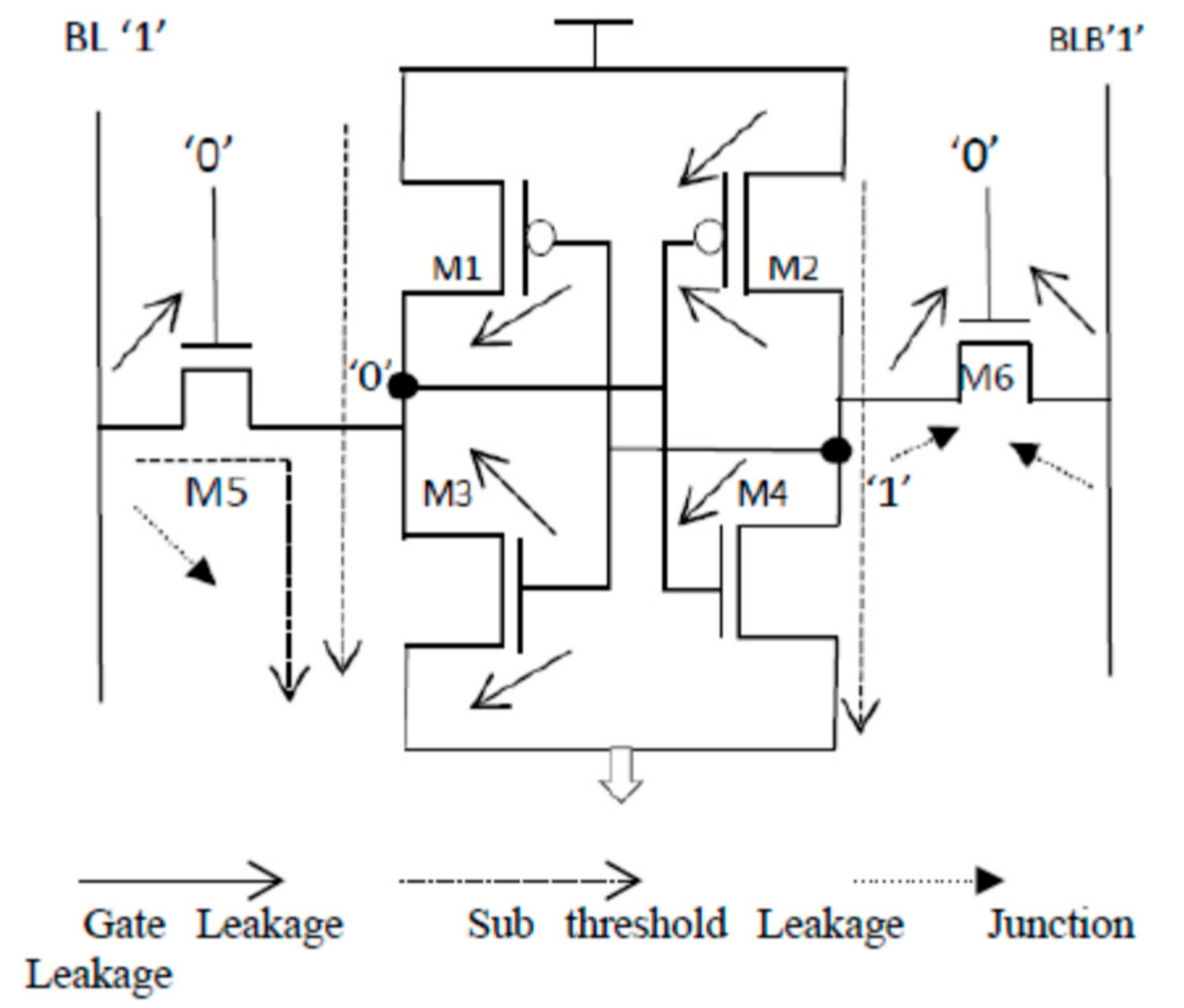
Figure 1 shows the circuit for a CMOS 6T SRAM cell. It contains two inverters formed by transistors M1, M3 and M2, and M4. The two access transistors used are M5 and M6, which are enabled by word-line (WL). It also uses two complimentary bit-lines, BL and BLB. These act as input/output lines that carry data to/from the memory cell.
For the SRAM cell shown in Figure 1, the two dominant sub-threshold leakage paths are:
- Supply voltage VDD to ground.
- Bitlines to ground, through access transistors M5 and M6.
3. SRAM Cell Stability
The SNM is used to measure the stability of an SRAM cell and is defined by the maximum DC noise that can be tolerated by the memory cell before flipping its state [6].
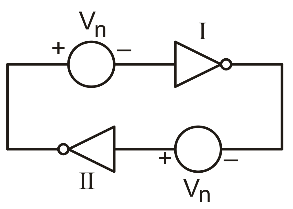
Figure 2 shows an alternative structure that can be used to measure the SNM of a memory cell. The two back-to-back connected inverters must maintain a bi-stable operating point to hold the data in the cell properly.
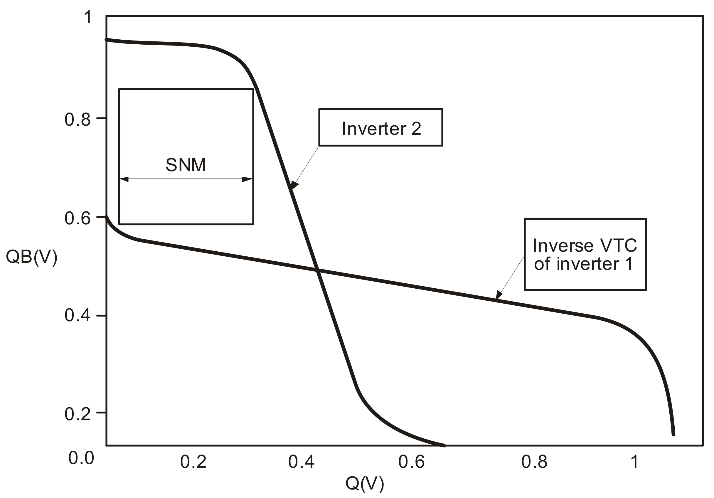
The SNM of an SRAM cell can be obtained by using a ‘butterfly curve’ as shown in Figure 3. The curve can be obtained by plotting the voltage transfer characteristics (VTC) of inverter 2 and the inverse VTC of inverter 1 on the same plot window. The resulting two lobe curve is called a ‘butterfly curve’. SNM is defined as the length of the side of the largest square that can be embedded inside the lobes of the butterfly curve [7].
SNM Dependences
The noise tolerating capability of an SRAM cell largely determines the stability of the cell to retain its data. It is measured by the SNM, which in turn depends on device parameters like supply voltage, cell ratio (CR), pull-up ratio (PR), threshold voltage of the device and temperature. The cell ratio is the ratio between the size of the driver transistor to the access transistor during the read operation, and PR is the ratio between the size of the load transistor to the access transistor during write operation [8], as shown in Figure 1.
CR = (W3/L3) n/(W5/L5) n (During Read Operation)
PR = (W2/L2) p/(W6/L6) n (During Write Operation)
It is observed that for a 6T SRAM cell, the SNM can be improved by increasing the cell ratio and pull-up ratio of the cell, but increasing these also results in an increase in leakage current and power dissipation [9].
4. Related Work
Various techniques for leakage reduction and SNM improvement have been proposed. SNM improvement techniques mainly include transistor width modulation, word-line voltage modulation and bit-line voltage modulation. Some techniques [10,11,12,13,14] when applied to the memory cell may lead to contradictory effects; for example, improvement in stability is obtained at the cost of area or leakage power, so optimization of various parameters as per the requirement is a challenge.
Several widely used techniques for leakage reduction in memory cells includes biasing techniques, which include both forward body biasing (FBB) [15] and reverse body biasing (RBB) [16,17,18]. Both techniques vary the threshold voltage of a MOS transistor by varying the body bias, as substrate voltage determines the threshold voltage of a transistor and this in turn affects the leakage current and stability of the circuit. The other techniques include dual threshold voltage (VTH) [19], variable threshold voltage CMOS (VTCMOS) [20,21] and stacking of transistors [22]. To improve upon the stability of the SRAM cell transistor width modulation effect, word-line modulation and bit-line modulation can be used. It is observed that stability of the memory cell can be improved by increasing CR, PR, bit-line voltage and word-line voltage.
A charge pump circuit can be integrated to harvest and reverse bit-line charge [23]; this helps to efficiently recycle the charge to achieve savings in leakage power and also demonstrates good read/write stability. The simulations performed for 180 nm CMOS technology show that there is 3.8% area overhead on comparison with 6T SRAM cell. Another approach to improve the stability of the SRAM cell is to use a 7T read disturbance free differential SRAM cell [24]. This technique isolates the read bit-lines from internal nodes, thereby consuming less energy, but at the cost of area overhead. An 8T SRAM cell with charge recycling read and write assist (CRRWA) technique [25] has also been presented, which reduces read and write energies when compared with 6T CMOS SRAM cells. This technique also introduces area overhead. Read decoupled partial feedback cutting 9T subthreshold SRAM cells (RDPFC 9T) [26] have been presented using the 65 nm technology node to lower the leakage power and achieve higher read stability than CMOS 6T SRAM cells. This design approach, however, has an area overhead of 1.45 times that of the 6T SRAM cell. A differential 10T bit-cell [27] is proposed, which separates the read and write operations to increase the stability of the cell while maintaining the leakage power close to that of the 6T SRAM cell, however it uses additional transistors. A Schmitt trigger (ST) based differential 10T SRAM cell [28] is also presented to improve read stability, but at the cost of area overhead.
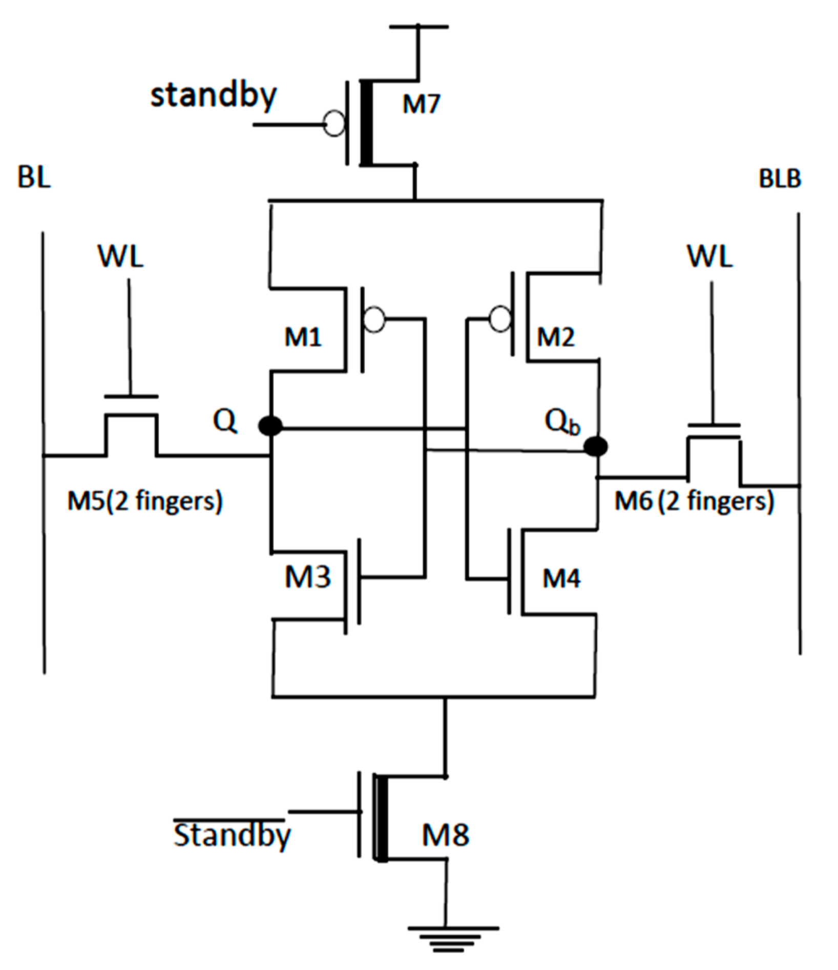
5. Proposed SRAM Cell
It has been shown that the MTCMOS technique can be used in a 6T SRAM cell to reduce the leakage in stand-by mode [27] and the use of two finger transistors in SRAM cell design can be used to reduce leakage [4]. This paper presents a new SRAM cell design which uses the two techniques in combination; the proposed cell improves the leakage current in stand-by mode and also improves the stability of the memory cell. Previous work [4,29] did not analyze the design effect on the SNM of the cell; in contrast, this paper discusses the effect of the proposed design on stability and SNM.
5.1. MTCMOS SRAM
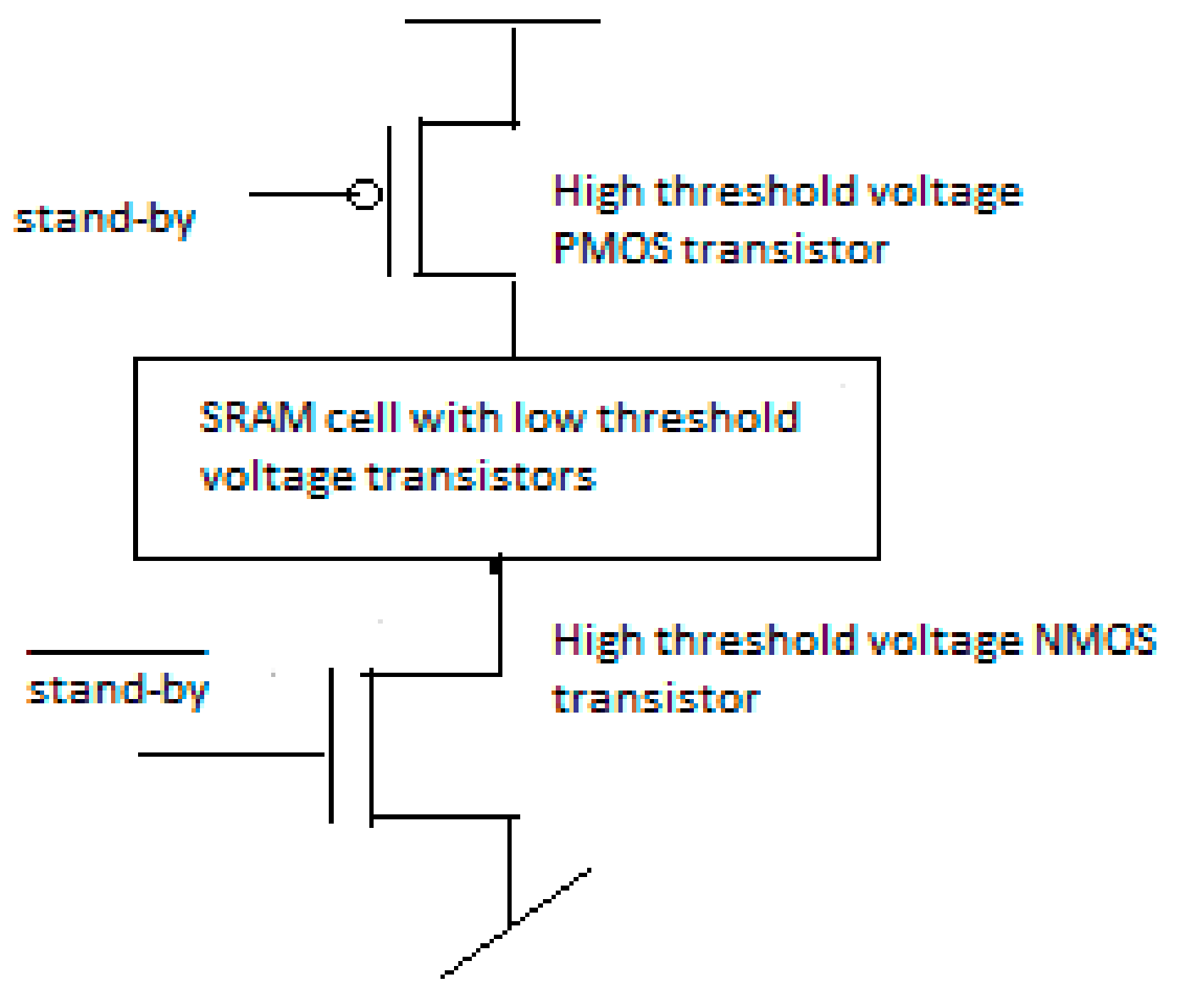
In the MTCMOS technique, two additional high threshold voltage (HVT) transistors (also referred to as sleep transistors) are inserted between the supply rails and the CMOS 6T SRAM cell. The cell is designed using low threshold voltage (LVT) transistors so that the delay of the cell is reduced even for lower supply voltage, which is used to reduce the power dissipation. However, a lower threshold voltage results in increased sub threshold conduction; hence, high threshold voltage sleep transistors are used to cut off the path for current to flow when the circuit is in stand-by mode. The circuit is shown in Figure 4.
This approach increases the number of transistors, but the overhead can be tolerated to improve the cell performance in terms of leakage current and delay.
5.2. Fingering in MOS Transistor
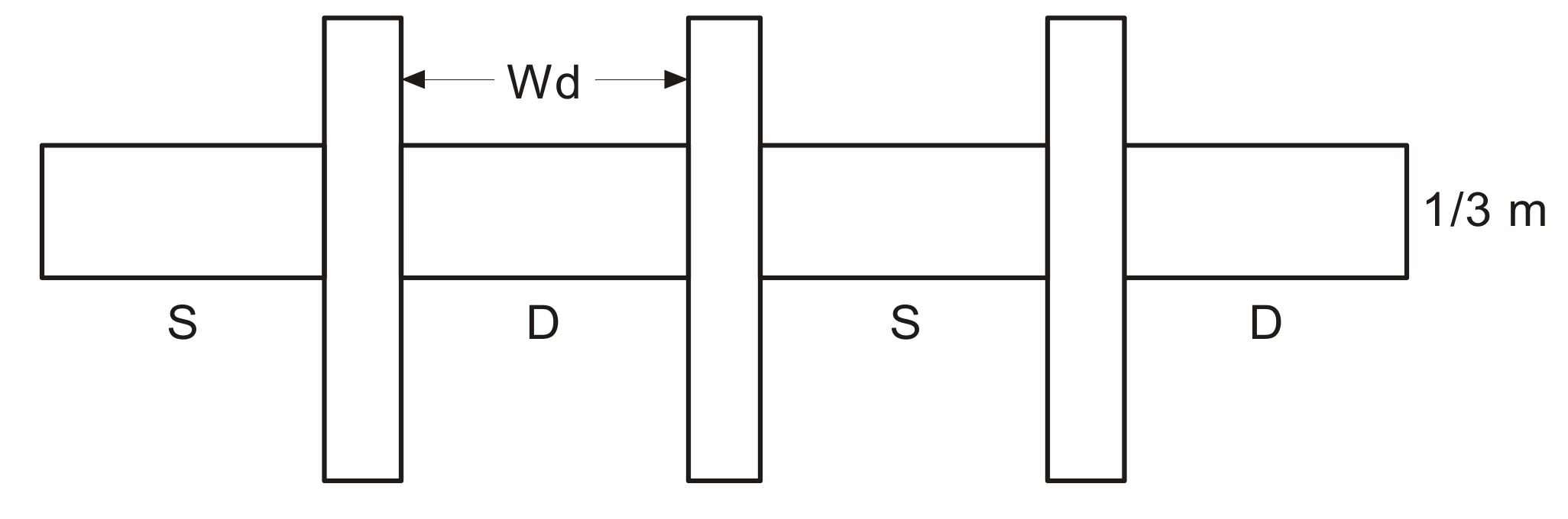
A multi finger transistor has many advantages over single finger transistors. It has lower gate resistance and is widely used in industry [30,31], however, an increasing number of fingers results in larger gate capacitance [32]. Figure 5 shows the multi finger technique layout design.
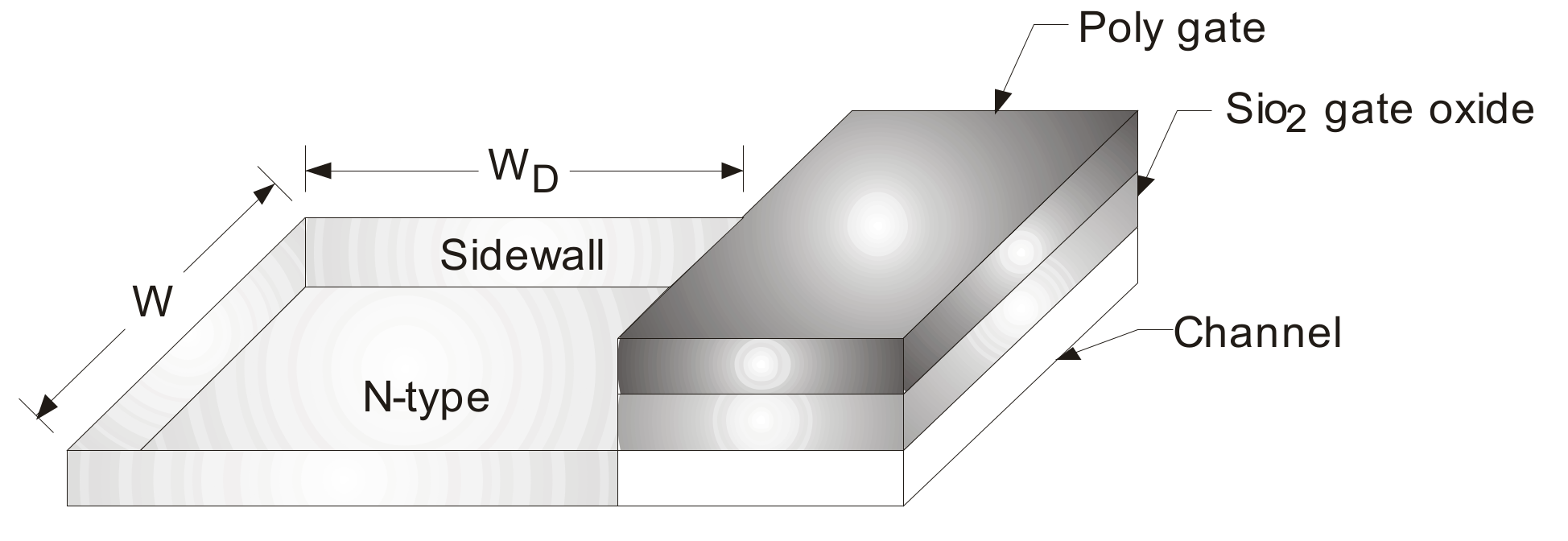
The number of fingers in a transistor and its capacitance can be analyzed from the three-dimensional (3D) transistor view of a MOS transistor, as shown in Figure 6.
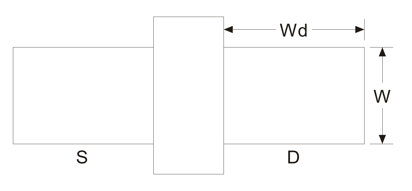
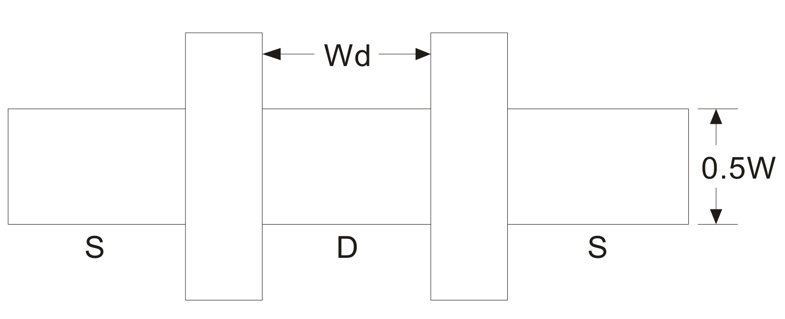
W is the width of the transistor and WD is the diffusion width required by fabrication. The value of W decreases as we increase the number of fingers. The finger width for a multi finger case can be considered as the value for W. Single transistors with one finger, two fingers and three fingers are shown in Figure 7, Figure 8 and Figure 9, respectively.
From Figure 6 and Figure 7, the calculations of area and perimeter of source and drain can be done for a one finger MOS transistor and is given in Equations (3) and (4) [33,34].
Area of drain = AD1 = Area of source = AS1 = W × WD
Perimeter of drain = PD1 = Perimeter of source = PS1 = W + 2WD
In the same way, the estimation of area and perimeter of drain and source can be done for two finger transistors:
Area of drain = AD2 = ½ (W × WD)
Area of source = AS2= ½ (W × WD) × 2 = W × WD
Perimeter of drain = PD2 = 2WD + W
Perimeter of source = Ps2 = 2(2WD + 0.5W) = 4WD + W
Similarly, the estimation of area and perimeter of drain and source for three finger transistors is given in Equations (10)–(13).
Area of drain = AD3 = 2 × (1/3) W × WD = (2/3) × W × WD
Area of source = AS3 = 2 × (1/3) W × Ws = (2/3) × W × Ws = (2/3) × W × WD = AD3
Perimeter of drain = PD3 = 2 × 2WD + (1/3)W = 4WD + W/3
Perimeter of source = Ps3 = 2 × 2Ws + (1/3)W = 4Ws +W/3 = 4WD +W/3 = PD3
When the number of fingers (Nf) is even = 2k (where k is an integer), the number of drain diffusion is k and the number of source diffusion is (k + 1) while the finger width reduces to W/2k, so the total area for drain diffusion is reduced by half and the perimeter is also less than the perimeter of a one finger transistor.
In the case of an odd number of fingers, Nf = 2k + 1, the transistors are divided into (k + 1) numbers of source and drain diffusion. So, multiple finger technology can enormously reduce the diffusion area and perimeter. Hence, this technique can be used to improve upon the leakage and stability of the memory cell.
6. Results and Discussion
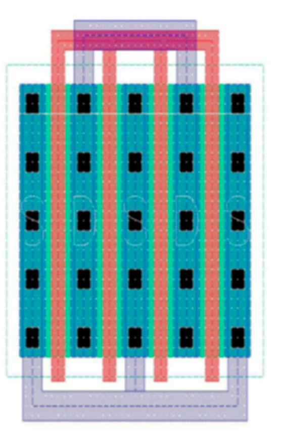
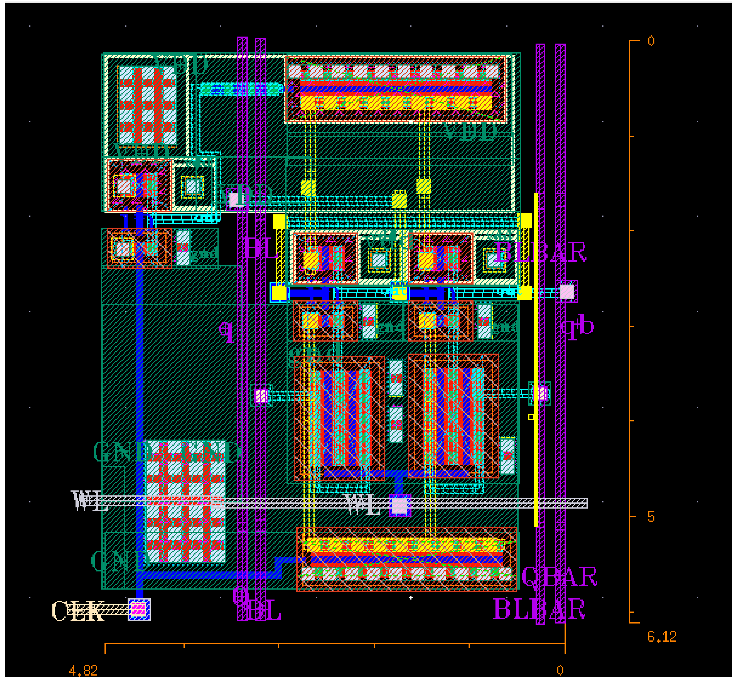
In this paper, we have used a two finger MOS transistor as the access transistor of the 6T MTCMOS SRAM cell This proposed design is compared with conventional 6T SRAM cells and also with MTCMOS SRAM cells with all the MOS transistors having one finger. The circuit diagram of the proposed SRAM cell is shown in Figure 10. It uses two high threshold voltage (HVT) transistors (M7 and M8), while the SRAM cell is designed with low threshold voltage (LVT) transistors. The access transistors (M5 and M6) are also LVT and hasand two fingers. The specifications for the proposed cell are given in Table 1.
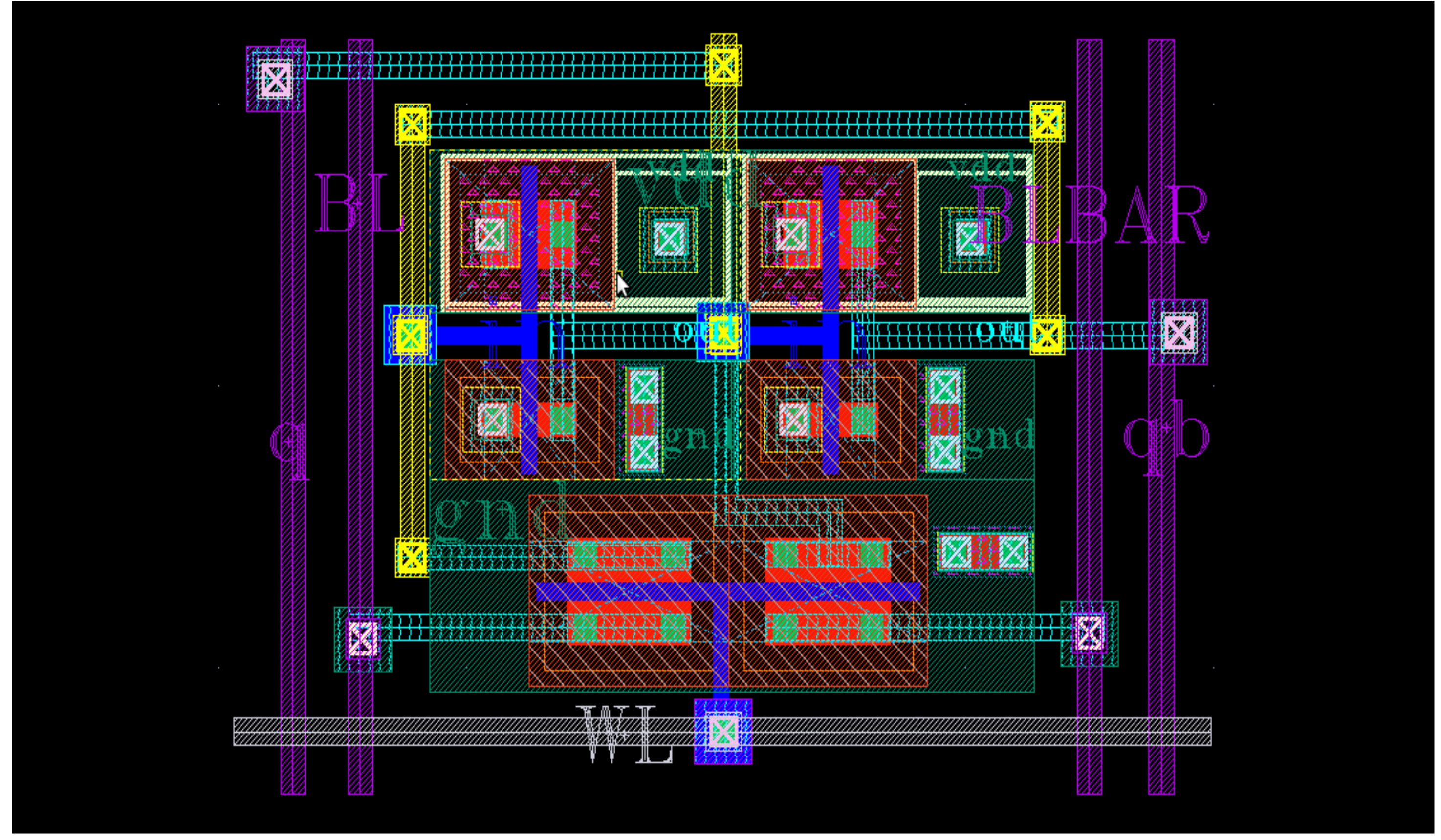
The schematic of the 6T SRAM cell is designed and the layout generated is shown in Figure 11. The design is simulated to calculate the SNM and leakage power. The schematic for the MTCMOS SRAM cell is then designed and the layout generated is shown in Figure 12. Leakage current and the SNM are then obtained.
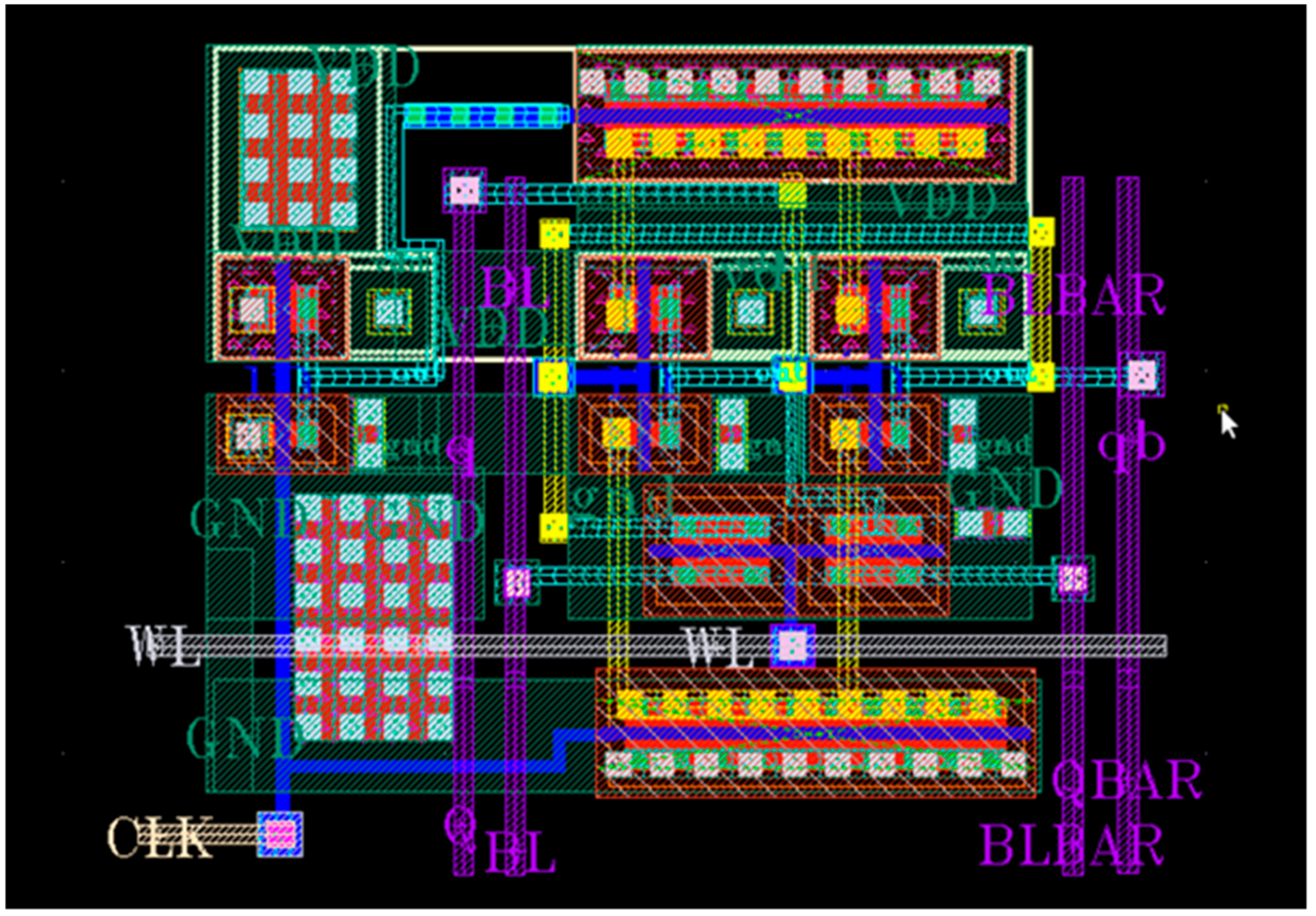
Then the proposed SRAM cell as shown in Figure 10 is designed and simulated for SNM and leakage calculation. The layout of the same is also generated to look into area overhead. The proposed cell was simulated to calculate the read static noise margin (RSNM) and the write static noise margin (WSNM). The read static noise margin (RSNM) is a measure of how much noise voltage is required at the node storing “0” to flip the state of an SRAM cell while reading. Therefore, RSNM is a more critical design metric of SRAM cells than SNM. The write static noise margin (WSNM) is another SRAM cell design metric, which implies the write ability of an SRAM cell. It is a measure of the ability of the cell to pull down the node storing “1” to a voltage less than the switching threshold voltage of the other inverter storing “0”, so that flipping of the cell state occurs. WSNM is measured while writing “1”. The layout of a proposed SRAM cell that uses an NMOS access transistor with two fingers is designed and shown in Figure 13. The leakage current, RSNM and WSNM were also obtained for the proposed cell. All design and simulation was done using the Cadence Virtuoso tool at 55 nm UMC technology. The results obtained for the proposed cell are compared to the SRAM cell mentioned in [27,28,29]. The comparative analysis of different parameters is given in Table 2.
Table 2 shows the comparison of the proposed SRAM cell with other SRAM cells.
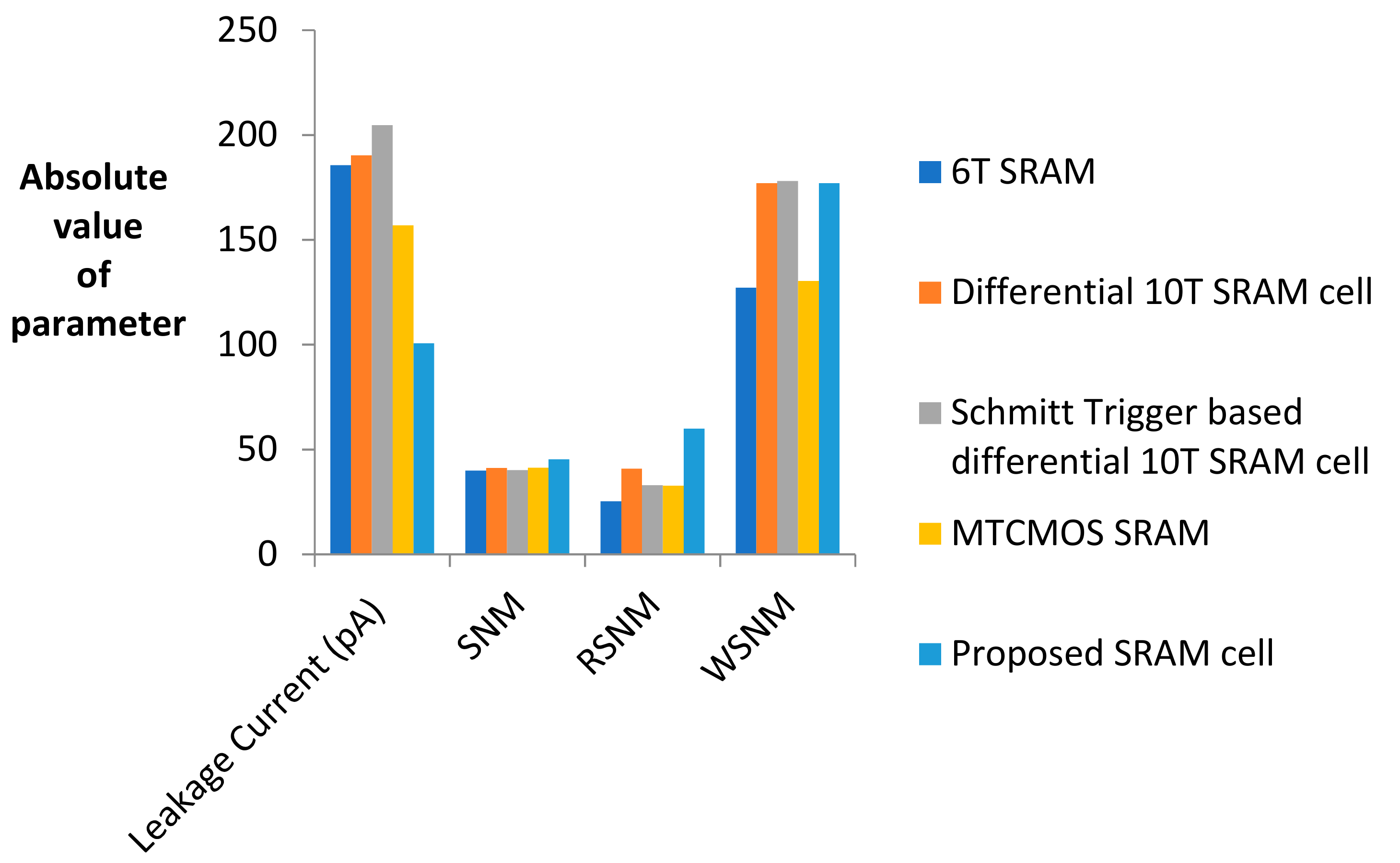
The proposed cell is simulated and compared with other cells for different parameters like leakage current, SNM, RSNM and WSNM. Table 2 clearly indicates that the proposed SRAM cell largely improves the RSNM and leakage current of the SRAM cell by using only eight transistors in contrast to the other cells, which use 10 transistors in their design. Hence, it can be used to design a low leakage SRAM cell with improved stability and slight area overhead that can be tolerated in applications with tight constraints on stability and higher battery life.
Table 3 shows the comparison in terms of area for the proposed SRAM cell with MTCMOS and a conventional SRAM cell.
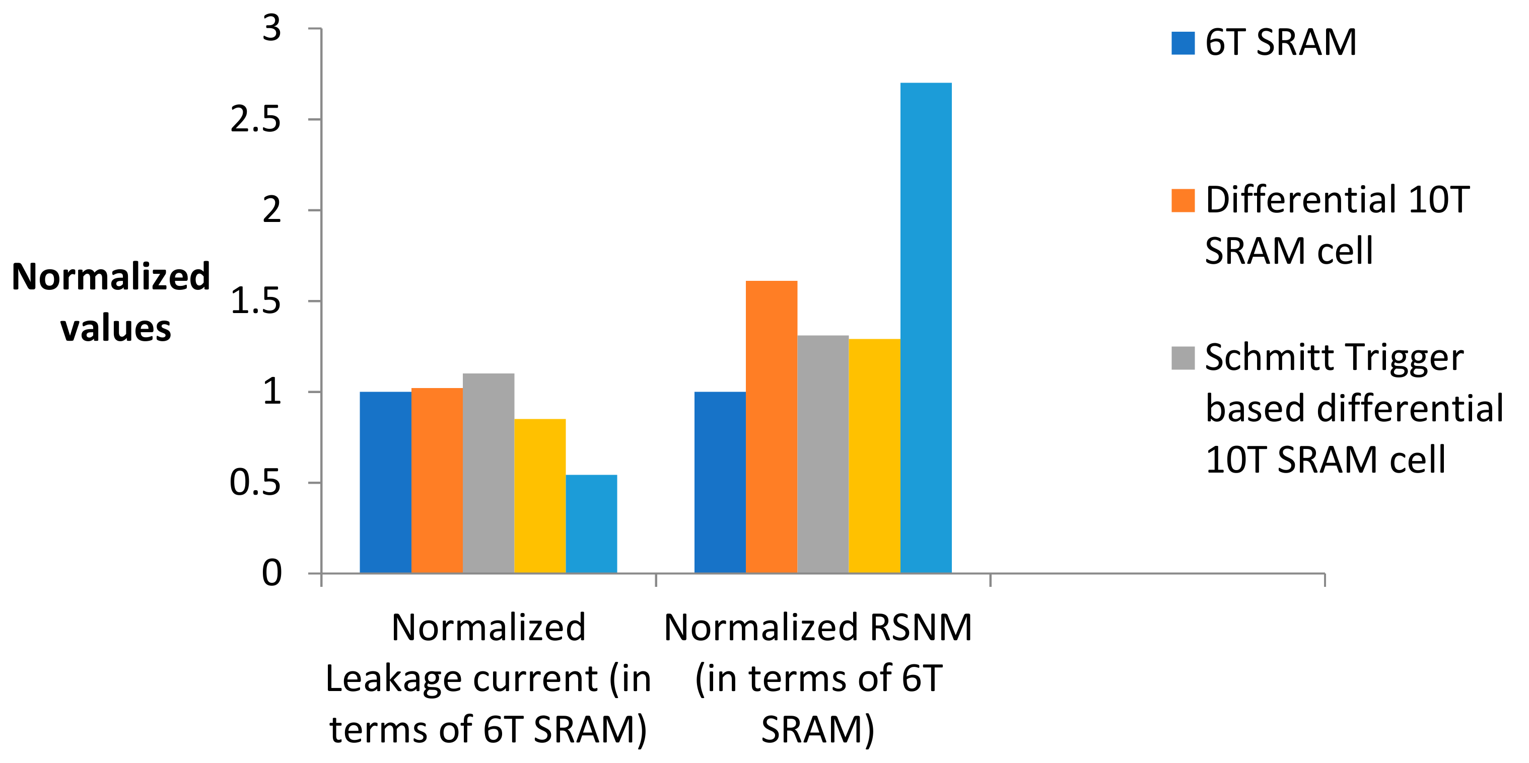
The comparative analysis for leakage current, SNM, WSNM and RSNM is shown graphically in Figure 14. Two of these parameters, RSNM and leakage current, show significant improvement and their values when normalized in terms of the 6T SRAM cell are plotted in Figure 15.
The graphical analysis of Figure 15 shows considerable improvement in the RSNM and leakage current when compared with conventional 6T SRAM cell.
7. Conclusions
Memory cell design with low leakage and high stability is the prime concern of the electronics industry. There are various techniques that have been proposed for leakage reduction as well as stability improvement. This paper presents a new design approach to reduce the leakage current in SRAM cells while maintaining good stability. There is almost 2.7 times improvement in read stability and 1.85 times improvement in leakage current with the use of the proposed SRAM cell, however there is area overhead that can be tolerated due to improvement in important design metrics of the SRAM cell.
Author Contributions
Conceptualization and methodology, T.T. and S.K.S.; writing-review and editing, T.T.; conceptualization and supervision, D.S.C.
Funding
This research received no external funding.
Conflicts of Interest
The authors declare no conflict of interest.
References
- Takeda, K.; Hagihara, Y.; Aimoto, Y.; Nomura, M.; Nakazawa, Y.; Ishii, T.; Kobatake, H. A read-static-noise-margin-free SRAM cell for low-VDD and high-speed applications. IEEE J. Solid-State Circuits 2006, 41, 113–121. [Google Scholar] [CrossRef]
- Itoh, K.; Sasaki, K.; Nakagome, Y. Trends in low-power RAM circuit technologies. Proc. IEEE 1995, 83, 524–543. [Google Scholar] [CrossRef]
- Singh, S.K.; Kaushik, B.K. A novel approach to reduce leakage current in ULP SRAM. IETE J. Res. 2013, 59, 704–708. [Google Scholar] [CrossRef]
- Singh, S.K.; Kaushik, B.K.; Chauhan, D.S. A novel approach to reduce sub threshold leakage in deep sub-micron SRAM. World Appl. Sci. J. 2013, 22, 442–446. [Google Scholar]
- Tripathi, T.; Chauhan, D.S.; Singh, S.K. Low Leakage SRAM for ULP applications. Int. J. Electron. Technol. 2018, 7, 2521–2524. [Google Scholar]
- Lohstroh, J.; Seevinck, E.; De Groot, J. Worst-case static noise margin criteria for logic circuits and their mathematical equivalence. IEEE J. Solid-State Circuits 1983, 18, 803–807. [Google Scholar] [CrossRef]
- Grossar, E.; Stucchi, M.; Maex, K.; Dehaene, W. Read stability and write-ability analysis of SRAM cells for nanometer technologies. IEEE J. Solid-State Circuits 2006, 41, 2577–2588. [Google Scholar] [CrossRef]
- Rahman, N.; Dhiman, G.; Singh, B.P. Static-noise-margin analysis of modified 6t SRAM cell during read operation. Int. J. Recent Trends Eng. Tech. 2013, 8, 47. [Google Scholar]
- Scientist-E, C.D.A.C.; Noida, U.P. Characterization and comparison of low power SRAM cells. J. Electron Devices 2011, 11, 560–566. [Google Scholar]
- Dhilleswararao, P.; Mahapatra, R.; Srinivas, P.S.T.N. High SNM 32nm CNFET based 6T SRAM Cell design considering transistor ratio. In Proceedings of the Electronics and Communication Systems (ICECS), Coimbatore, India, 13–14 February 2014; pp. 1–6. [Google Scholar]
- Karthika, S.; SivaMangai, N.M. Power analysis of bit interleaving 9T SRAM array. In Proceedings of the 2016 3rd International Conference on Devices, Circuits and Systems (ICDCS), Coimbatore, India, 3–5 March 2016; pp. 275–280. [Google Scholar]
- Ahmad, S.; Gupta, M.K.; Alam, N.; Hasan, M. Single-ended Schmitt-trigger-based robust low-power SRAM cell. IEEE Trans. Very Large Scale Integr. (VLSI) Syst. 2016, 24, 2634–2642. [Google Scholar] [CrossRef]
- Nayak, D.; Acharya, D.P.; Mahapatra, K. Current starving the SRAM Cell: A strategy to improve cell stability and power. Circuits Syst. Signal Process. 2017, 36, 3047–3070. [Google Scholar] [CrossRef]
- Manna, A.; Bhaaskaran, V.K. Improved read noise margin characteristics for single bit line SRAM cell using adiabatically operated word line. In Proceedings of the 2017 International Conference on Nextgen Electronic Technologies: Silicon to Software (ICNETS2), Chennai, India, 23–25 March 2017; pp. 385–393. [Google Scholar]
- Deshmukh, J.; Khare, K. Dynamic SVL and body bias for low leakage power and high performance in CMOS digital circuits. Int. J. Electron. 2012, 99, 1717–1728. [Google Scholar] [CrossRef]
- Karuppanan, P.; Ghosh, S.R.; Khan, K.; Bikki, P.K. A fully differential operational amplifier with slew rate enhancer and adaptive bias for ultra low power. J Low Power Electron. 2017, 13, 67–75. [Google Scholar] [CrossRef]
- Enomoto, T.; Oka, Y.; Shikano, H.; Harada, T. A self–controllable–voltage–level (SVL) circuit for low–power, high–speed CMOS circuits. In Proceedings of the 28th European Solid-State Circuits Conference, Firenze, Italy, 24–26 September 2002; pp. 411–414. [Google Scholar]
- Enomoto, T.; Oka, Y.; Shikano, H. A self-controllable voltage level (SVL) circuit and its low-power high-speed CMOS circuit applications. IEEE J. Solid-State Circuits 2003, 38, 1220–1226. [Google Scholar] [CrossRef]
- Amelifard, B.; Fallah, F.; Pedram, M. Leakage minimization of SRAM cells in a dual-V t and Dual-T ox technology. IEEE Trans. Very Large Scale Integr. Syst. 2008, 16, 851–860. [Google Scholar] [CrossRef]
- Kuroda, T.; Fujita, T.; Mita, S.; Nagamatsu, T.; Yoshioka, S.; Suzuki, K.; Sano, F.; Norishima, M.; Murota, M.; Kako, M.; et al. A 0.9-V, 150-MHz, 10-mW, 4 mm/sup 2/, 2-D discrete cosine transform core processor with variable threshold-voltage (VT) scheme. IEEE J. Solid-State Circuits 1996, 31, 1770–1779. [Google Scholar] [CrossRef]
- Mizuno, H.; Ishibashi, K.; Shimura, T.; Hattori, T.; Narita, S.; Shiozawa, K.; Ikeda, S.; Uchiyama, K. An 18-/spl mu/A standby current 1.8-V, 200-MHz microprocessor with self-substrate-biased data-retention mode. IEEE J. Solid-State Circuits 1999, 34, 1492–1500. [Google Scholar] [CrossRef]
- Venigalla, S.P.; Swaroop Vemana, G.S.; Babu, M.N. To reduce SRAM sub-threshold leakage using stack and zig-zag techniques. Int. J. Sci. Eng. Technol. 2012, 1, 51–54. [Google Scholar]
- Wang, X.; Zhang, Y.; Lu, C.; Mao, Z. Power efficient SRAM design with integrated bit line charge pump. AEU-Int. J. Electron. Commun. 2016, 70, 1395–1402. [Google Scholar] [CrossRef]
- Nayak, D.; Acharya, D.P.; Mahapatra, K. A read disturbance free differential read SRAM cell for low power and reliable cache in embedded processor. AEU-Int. J. Electron. Commun. 2017, 74, 192–197. [Google Scholar] [CrossRef]
- Nayak, D.; Acharya, D.P.; Rout, P.K.; Nanda, U. A novel charge recycle read write assist technique for energy efficient and fast 20nm 8T-SRAM array. Solid State Electron. 2018, 148, 43–50. [Google Scholar] [CrossRef]
- Sharma, V.; Gopal, M.; Singh, P.; Vishvakarma, S.K. A 220 mV robust read-decoupled partial feedback cutting based low-leakage 9T SRAM for Internet of Things (IoT) applications. AEU-Int. J. Electron. Commun. 2018, 87, 144–157. [Google Scholar] [CrossRef]
- Chang, I.J.; Kim, J.J.; Park, S.P.; Roy, K. A 32kb 10T subthreshold SRAM array with bit-interleaving and differential read scheme in 90 nm CMOS. In Proceedings of the IEEE International Solid-State Circuits Conference, San Francisco, CA, USA, 3–7 February 2008; pp. 388–622. [Google Scholar]
- Kulkarni, J.P.; Kim, K.; Roy, K. A 160 mV robust Schmitt trigger based subthreshold SRAM. IEEE J. Solid-State Circuits 2007, 42, 2303–2313. [Google Scholar] [CrossRef]
- Tripathi, T.; Chauhan, D.S.; Singh, S.K.; Singh, S.V. Implementation of low power 6T SRAM cell using MTCMOS technique. In Proceedings of the International Conference on Communication and Computing Systems (ICCCS 2016), Ajmer, India, 9–11 September 2016. [Google Scholar]
- Kang, M.; Yun, I. Modeling electrical characteristics for multi-finger MOSFETs based on drain voltage variation. Trans. Electr. Electron. Mater. 2011, 12, 245–248. [Google Scholar] [CrossRef]
- Borkar, S.; Karnik, T.; Narendra, S.; Tschanz, J.; Keshavarzi, A.; De, V. Parameter variations and impact on circuits and microarchitecture. In Proceedings of the 40th annual Design Automation Conference, Anaheim, CA, USA, 2–6 June 2003; pp. 338–342. [Google Scholar] [Green Version]
- Nguyen, T.K.; Kim, C.H.; Ihm, G.J.; Yang, M.S.; Lee, S.G. CMOS low-noise amplifier design optimization techniques. IEEE Trans. Microw. Theory Tech. 2004, 52, 1433–1442. [Google Scholar] [CrossRef]
- Martin, K. Digital Integrated Circuit Design; Oxford University Press: Oxford, UK, 1999. [Google Scholar]
- Rabaey, J.M.; Chandrakasan, A.P.; Nikolić, B. Digital Integrated Circuits, 2ed ed.; Prentice Hall: Upper Saddle River, NY, USA, 2003. [Google Scholar]
Figure 1.
Complementary metal oxide semiconductor (CMOS) 6T static random-access memory (SRAM) cell. M1–4 = transistors. M5–6 = access transistors.
Figure 1.
Complementary metal oxide semiconductor (CMOS) 6T static random-access memory (SRAM) cell. M1–4 = transistors. M5–6 = access transistors.

Figure 2.
Flip flop comprising two inverters (I and II); static noise voltage sources (Vn) are included.
Figure 2.
Flip flop comprising two inverters (I and II); static noise voltage sources (Vn) are included.

Figure 3.
Butterfly curve for obtaining the static noise margin (SNM).

Figure 4.
Multi-threshold CMOS (MTCMOS) SRAM cell.

Figure 5.
Multi finger transistor layout.

Figure 6.
Three-dimensional (3D) view of MOS transistor diffusion. W = the width of the transistor; WD = the diffusion width required by fabrication.
Figure 6.
Three-dimensional (3D) view of MOS transistor diffusion. W = the width of the transistor; WD = the diffusion width required by fabrication.

Figure 7.
One finger single MOS transistor.

Figure 8.
Two finger single MOS transistor.

Figure 9.
Three finger single MOS transistor.

Figure 10.
Proposed SRAM cell.

Figure 11.
Layout of a conventional 6T SRAM cell.

Figure 12.
Layout of MTCMOS SRAM cell.

Figure 13.
Layout of the proposed SRAM cell.

Figure 14.
Comparison of absolute values of different parameters.

Figure 15.
Comparison of leakage current and RSNM (normalized in terms of 6T SRAM cell).


Table 1.
Specifications for Figure 11 (proposed SRAM cell).
Table 1.
Specifications for Figure 11 (proposed SRAM cell).
| Transistor Name | W/L Ratio | Type | Fingers |
|---|---|---|---|
| M1, M2 | 4 | Low VT PMOS | 1 |
| M3, M4, M5, M6 | 2 | Low VT NMOS | 1 |
| M7 | 4 | Low VT PMOS | 2 |
| M8 | 2 | Low VT PMOS | 2 |
Table 2.
Comparison of the proposed SRAM cell. RSNM = read SNM. WSNM = write SNM.
| Parameter | CMOS 6T SRAM Cell | Differential 10T SRAM Cell ([27]) | Schmitt Trigger Based Differential 10T SRAM Cell ([28]) | MTCMOS 6T SRAM Cell ([29]) | Proposed SRAM Cell |
|---|---|---|---|---|---|
| Technology (nm) | 55 | 55 | 55 | 55 | 55 |
| VDD (V) | 0.6 | 0.6 | 0.6 | 0.6 | 0.6 |
| Leakage Current (pA) | 185.57 | 190.25 | 204.65 | 156.87 | 100.631 |
| Normalized Leakage current (in terms of 6T SRAM) | 1 | 1.02 | 1.10 | 0.85 | 0.542 |
| SNM | 39.87 | 41.18 | 40.12 | 41.25 | 45.32 |
| RSNM | 25.31 | 40.78 | 32.9 | 32.67 | 59.94 |
| Normalized RSNM (in terms of 6T SRAM) | 1 | 1.61 | 1.3 | 1.29 | 2.7 |
| WSNM | 127.12 | 176.95 | 177.99 | 130.33 | 176.98 |
| Number of transistors used | 6 | 10 | 10 | 8 | 8 |
Table 3.
Area comparison of the proposed SRAM cell.
| Parameter | CMOS 6T SRAM cell | MTCMOS 6T SRAM Cell ([29]) | Proposed SRAM Cell |
|---|---|---|---|
| Technology (nm) | 55 | 55 | 55 |
| VDD (V) | 0.6 | 0.6 | 0.6 |
| Area (um2) | 10.08 | 11.55 | 27.2 |
| Normalized area in terms of 6T SRAM | 1 | 1.14 | 2.69 |
© 2018 by the authors. Licensee MDPI, Basel, Switzerland. This article is an open access article distributed under the terms and conditions of the Creative Commons Attribution (CC BY) license (http://creativecommons.org/licenses/by/4.0/).
Share and Cite
MDPI and ACS Style
Tripathi, T.; Chauhan, D.S.; Singh, S.K. A Novel Approach to Design SRAM Cells for Low Leakage and Improved Stability. J. Low Power Electron. Appl. 2018, 8, 41. https://0-doi-org.brum.beds.ac.uk/10.3390/jlpea8040041
AMA Style
Tripathi T, Chauhan DS, Singh SK. A Novel Approach to Design SRAM Cells for Low Leakage and Improved Stability. Journal of Low Power Electronics and Applications. 2018; 8(4):41. https://0-doi-org.brum.beds.ac.uk/10.3390/jlpea8040041
Chicago/Turabian StyleTripathi, Tripti, Durg Singh Chauhan, and Sanjay Kumar Singh. 2018. "A Novel Approach to Design SRAM Cells for Low Leakage and Improved Stability" Journal of Low Power Electronics and Applications 8, no. 4: 41. https://0-doi-org.brum.beds.ac.uk/10.3390/jlpea8040041
Note that from the first issue of 2016, this journal uses article numbers instead of page numbers. See further details here.