
Using SKPFM to Determine the Influence of Deformation-Induced Dislocations on the Volta Potential of Copper


1
College of Materials and Metallurgy, Guizhou University, Guiyang 550025, China
2
Key Laboratory for Mechanical Behavior and Microstructure of Materials of Guizhou Province, Guizhou University, Guiyang 550025, China
3
National & Local Joint Engineering Laboratory for High-Performance Metal Structure Material and Advanced Manufacturing Technology, Guizhou University, Guiyang 550025, China
*
Author to whom correspondence should be addressed.
Metals 2021, 11(8), 1166; https://0-doi-org.brum.beds.ac.uk/10.3390/met11081166
Submission received: 11 May 2021
/
Revised: 26 June 2021
/
Accepted: 20 July 2021
/
Published: 22 July 2021
Abstract
:The variation rule of the Volta potential on deformed copper surfaces with the dislocation density is determined in this study by using electron back-scattered diffraction (EBSD) in conjunction with scanning Kelvin probe force microscopy (SKPFM). The results show that the Volta potential is not linear in the dislocation density. When the dislocation density increases due to the deformation of pure copper, the Volta potential tends to a physical limit. The Volta potential exhibits a fractional function relationship with the dislocation density only for a relatively low shape variable.
1. Introduction
The Volta potential, as measured by scanning Kelvin probe force microscopy (SKPFM), has proven to be a useful quantity for assessing the (relative) nobility of local microstructures of an alloy to improve the understanding of localized corrosion and galvanic activities [1,2,3,4,5]. The magnitude of the Volta potential depends mainly on the electron work function (EWF) of metals: when applying a biased potential to a SKPFM tip, a noble metal with a higher EWF generally produces a more negative Volta potential [6].
Considerable effort has been expended in studying the mechanical effects of forces, such as stress and deformation, on EWFs over the past few decades. However, the effect of deformation on the electronic nature of metals remains unclear and considerably complex [7]. Scanning Kelvin probe technology (SKP) has mainly been used to determine the EWF [8,9]. SKP has disadvantages that need to be addressed. First, the effective spatial resolution of SKP is not sufficiently accurate to distinguish the potential difference between grains. The sampling distance from the metal surface for the potential measurement is limited to the submillimeter scale [7,10]. That is, the potential fluctuations measured by SKP are essentially averaged over dozens of grains. Second, the EWF is sensitive to surface geometrical configurations [10], such as the surface roughness [11] and microcracks [12], which can be regarded as an interference factor in SKP measurement.
The Volta potential map measured by SKPFM has recently gradually been introduced to analyze the localized electronic nature of metal surfaces [13]. SKPFM has a considerably higher spatial resolution than SKP, which can reach 10 nm in ambient air [14]. In addition, the atomic force microscopy (AFM) platform of the SKPFM precisely locks the tip-to-surface distance to a consistent value on the nanometer scale, which maximally eliminates interference from topographical factors. These advantages make SKPFM more suitable for analyzing the potential difference between grains or phases than SKP. Örnek et al. [15] used SKPFM to study the atmospheric corrosion behavior of 2205 dual-phase stainless steel and explained the preferential corrosion behavior of ferrite in terms of the interphase potential difference. A. Davoodi et al. [16] conducted a SKPFM study on the interfacial area between AA5083 and AA7023 for friction stir welding, and the results suggested the preferential corrosion of regions with high contact potential differences. Rahimi et al. [17] performed a study on a Cu-Ti welding area and found preferential dissolution of a Cu micro-area with a high Volta potential in the welding tissue with Ti.
The influence of dislocation proliferation induced by cold rolling deformation on the Volta potential was investigated in this study. To prevent composition-induced interference, pure copper was adopted and deformed by different degrees of cold rolling. The high spatial resolution of SKPFM was exploited in conjunction with EBSD. The deformed pure copper specimens were analyzed by scanning electron microscopy (SEM) with EBSD and then immediately transferred to an AFM platform to measure the Volta potential. Hence, the inverse pole figure (IPF) or low-angle boundary density map measured by EBSD was used to accurately focus the scanning area of the SKPFM probe on points of interest, such as grain boundaries and large deformation regions.
Li et al. [18] previously used a SKP probe to study the change in the EWF induced by deformation and found that the strain could reduce the EWF of the material. However, the aforementioned limitations of SKP have precluded the development of a quantitative model to explain how the dislocation density affects the EWF or Volta potential. Therefore, EBSD was combined with SKFPM in this study to statistically determine how the magnitude of the Volta potential varies with the measured dislocation density, and a quantitative model was proposed based on energy band theory.
2. Materials and Methods
2.1. Material and Heat Treatment
The experimental material was T2 copper, which is 99.92% Cu. A 40 mm × 40 mm × 10 mm piece of T2 copper was treated with a solid solution at 800 °C for 1 h to obtain relatively coarse equiaxed grains.
2.2. Rolling Deformation Technology
The solution-treated copper (T2) was cold-rolled in multiple passes at a speed of 300 r/min on a two-high mill. The original copper piece had an area of 40 mm × 40 mm and a thickness of 10 mm. The same rolling direction (RD) was maintained during the rolling process, with 2.5% deformation per pass. Multiple cold rolling passes yielded deformed copper with total deformations of 10%, 20% and 30%. Then the rolling coppers were machined to samples with 10 mm × 10 mm roller pressure surface.
2.3. Metallographic Observation
The cross sections of the samples were mechanically ground to 2500 grit using Sic paper, then the scratch-free surface was polished with 0.5 μm alumina powder dilution solution. Finally, the etching solution of 5 g FeCl3 + 10 mL HCl + 100 mL H2O was used for etching, The Olympus GX51 metallographic microscope (Olympus Corporation, Shen Zhen, China), was used to observe the microstructure at 20 times magnification.
2.4. EBSD Measurements
The microstructure and orientations of copper samples with different deformations were examined by using scanning electron microscopy (SEM)/EBSD. Prior to EBSD, the cross sections (RD-ND) of the samples were mechanically ground and polished to 4000 grit using Sic paper, then electro-polished in a chemical solution of 25% orthophosphoric acid, 25% ethanol and 50% distilled water at 10 V for 30 s at room temperature. The relatively deformation region and a step size of 0.5 μm were selected to investigate the microstructure by using a TESCAN MAIA3 XMH high-resolution SEM, (JEOL Inc., Peabody, MA, USA), at 20 kV and equipped with an OXFORD Nordlysmax3 EBSD detector, (Oxford instruments, Abingdon, UK), and a HKL Channel 5, (Oxford Instruments, Abingdon, UK) and the scanning area was 473 μm × 355 μm.
The surfaces of the polished copper samples with different deformations were marked with a microhardness tester on the hardness point of the XY axis to locate the position of a grain on the AFM platform after the EBSD test.
2.5. SKPFM Measurement
In order to minimize the effects of the metal passivation and adsorption on the variability of the acquired Volta potential values, after the EBSD test, the samples were stored in vacuum drying oven. In addition, prior to SKPFM imaging, the samples were cleaned by ultrasonication in ethanol for 60 s and then dried with compressed ultrahigh-purity (UHP) nitrogen gas.
A MultiMode 8 atomic force microscope was used to measure the Volta potential in the EBSD analysis area on the copper sample surface. The obtained data were analysed using Nano Scope Analysis V8.15 software developed by Bruker, Santa Barbara, CA, USA. The SKPFM measurements were carried out in ambient air at room temperature and 30% relative humidity, a pixel resolution of 256 × 256, and a scan frequency rate of 0.996 Hz, the scanning area was 20 μm × 20 μm. An SCM-PIT probe with a Pt coating was used. SKPFM was carried out in dual-scan mode, and the first scan (the main scan) was used to determine the sample morphology. The probe was raised by 80 nm, and a second scan was performed to obtain the Volta potential data. The working principles and technical details of SKPFM can be found in the literature [19,20]. The reliability of the probe was verified by measuring the Volta potential for standard Al samples before and after the experiment within one day and in the same test environment. The Volta potential of standard Al was found to only vary by 1~3 mV, without significant fluctuations, proving that the experimental probe was of good quality and had a maximal sensitivity for the system.
Based on the SKPFM working principle, the Volta potential difference between the specimen and tip (with bias) can be expressed as given below.
where ψs is the Volta potential of the sample, ψT is the Volta potential of the probe tip and Vcpd is the measured Volta potential difference. A bias voltage is applied to the probe tip during the experiment, therefore, when the measured Volta potential difference was positive, it indicates the Volta potential of the samples was lower to the tip and it can be inferred that the sample is less noble (anodic) than the tip [21]. Hence, in order to obtain the Volta potential (ψs) in the local area of the sample in the experiment, based on formula (1), the measured results of potential difference were reversed [22,23].
3. Result
3.1. The Influence of the Tip-to-Surface Distance on the Volta Potential
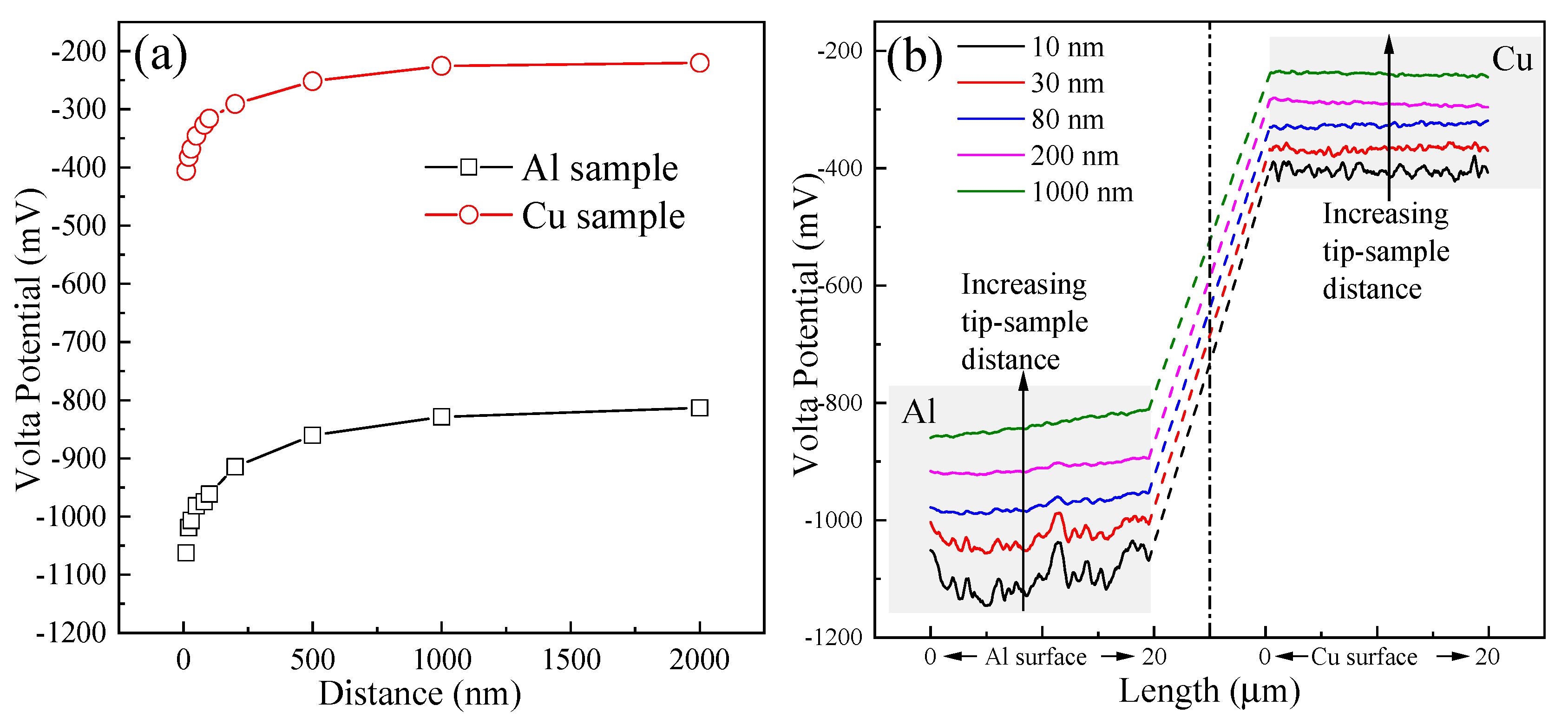
Rohwerder et al. has explained in detail how the SKFM measurement principle leads to high precision in microscale potential analysis, where the Volta potential is highly sensitive to the distance between the probe and the surface [2]. Figure 1a shows the change in the potential between the probe and metallic Cu and standard Al samples as a function of distance. There is a very strong interaction when the probe-sample distance is less than 500 nm that significantly changes the Volta potential, whereas there is very little change in the Volta potential for probe-sample distances above 500 nm. Thus, the SKPFM measurement is invalid for large probe-sample distances. The surface morphology, chemical composition and tissue structure have been reported to affect the Volta potential at small sample-probe distances [24]. Figure 1b shows tip-Al and tip-Cu electron couples, where the electric potential value fluctuates significantly upon decreasing the probe-sample distance, especially to 10 nm. These fluctuations become weak upon increasing the probe-sample distance to beyond 80 nm.
Ornek, C. et al. [2] considered the ideal distance of copper surface potential value measurement to be 50 to 100 nm. The experimental data analysis shows that 80 nm is the appropriate probe-sample distance to measure the Volta potential on a Cu surface using SKPFM.
3.2. EBSD Analysis of Copper with Different Rolling Deformations
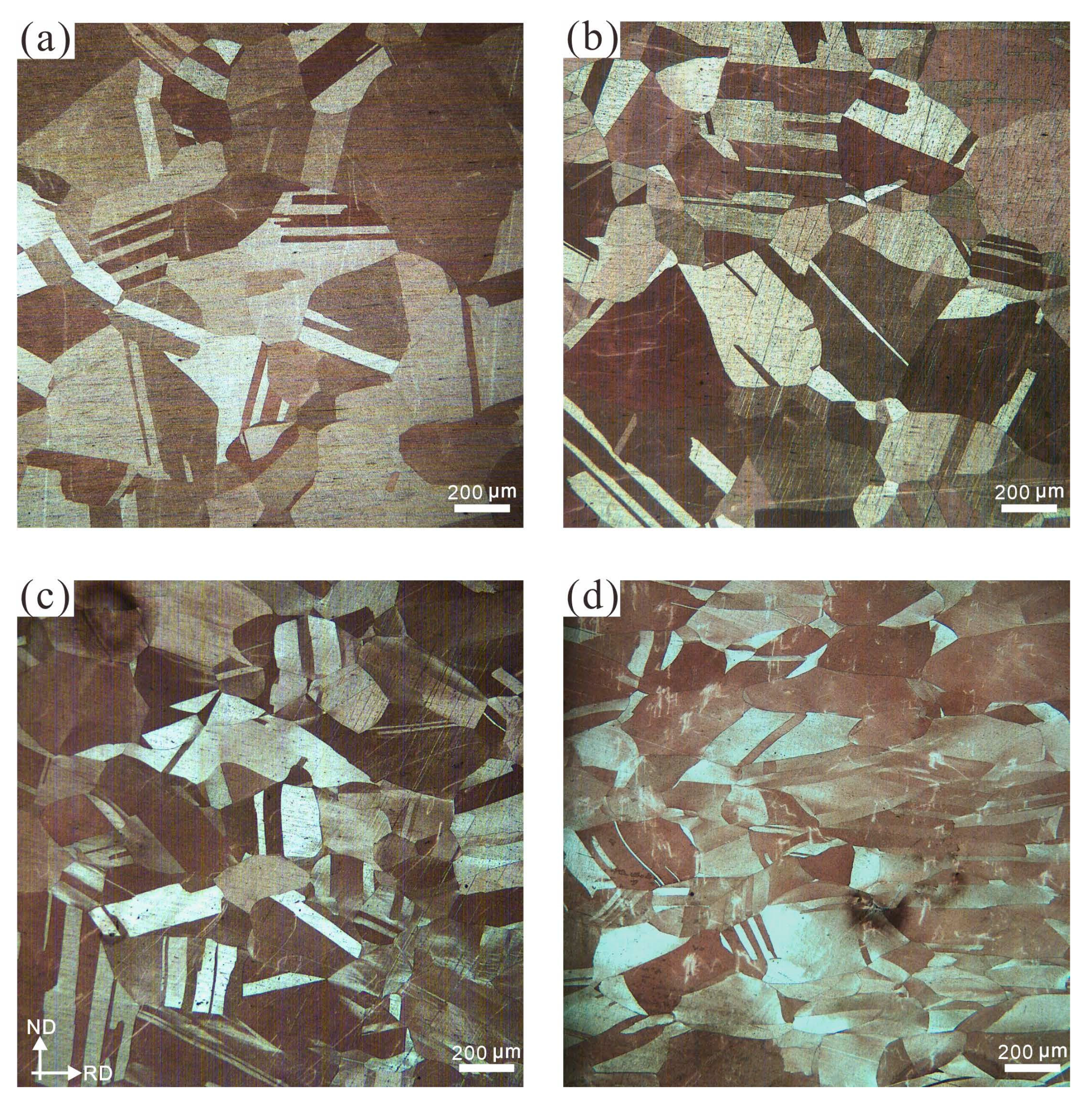
After solid solution treatment, the Cu was deformed by cold rolling to different degrees, and the metallographic diagram is shown in Figure 2. The undeformed grain size of copper reached up to 300 μm, where the large copper grain size was designed to enable precise positioning during subsequent probe scanning. As the compression degree increased, the copper grains gradually became refined and elongated, and the grain orientation gradually tends to the rolling direction.
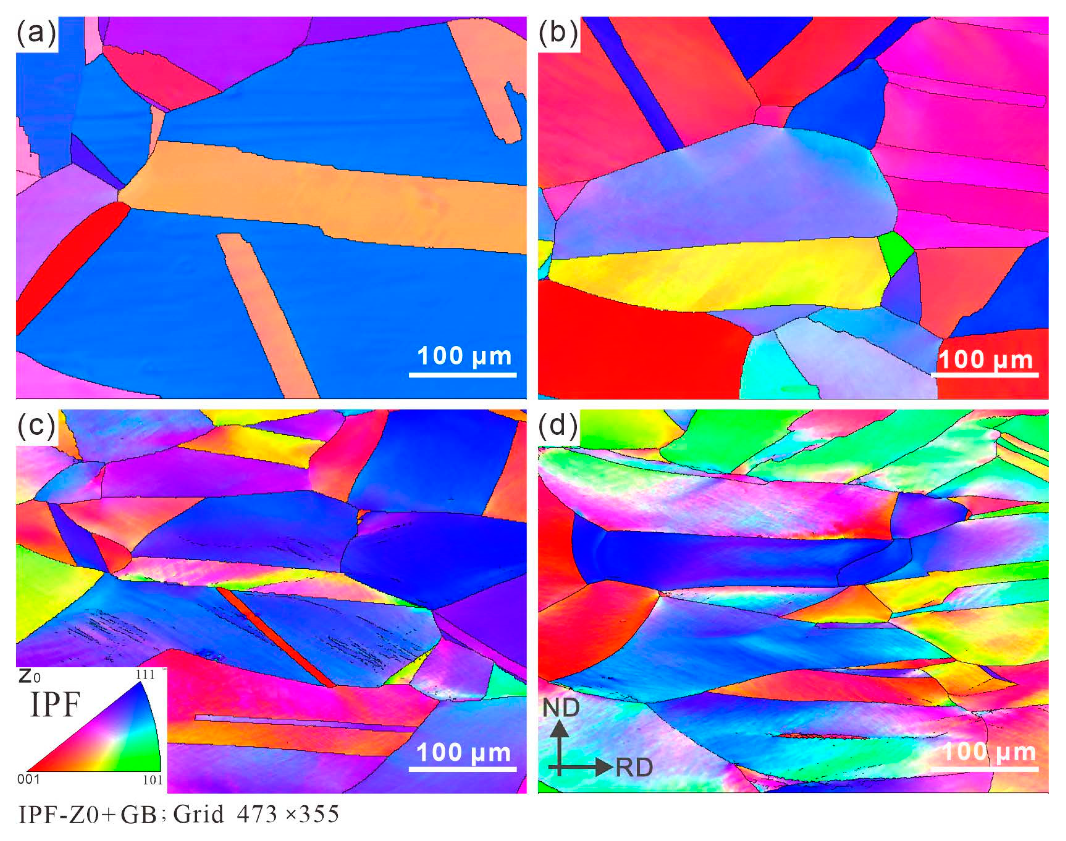
In the process of metal rolling, the increase of grain boundary length and the change of grain orientation are inevitable [25]. Figure 3 shows IPF graphs of copper cross section (RD-ND) under different rolling deformations. In Figure 3a, the original grains are disorderly equiaxed grains with a large difference in orientation. As the rolling deformation increases, the grains grow gradually in the rolling direction under the action of the compressive stress.
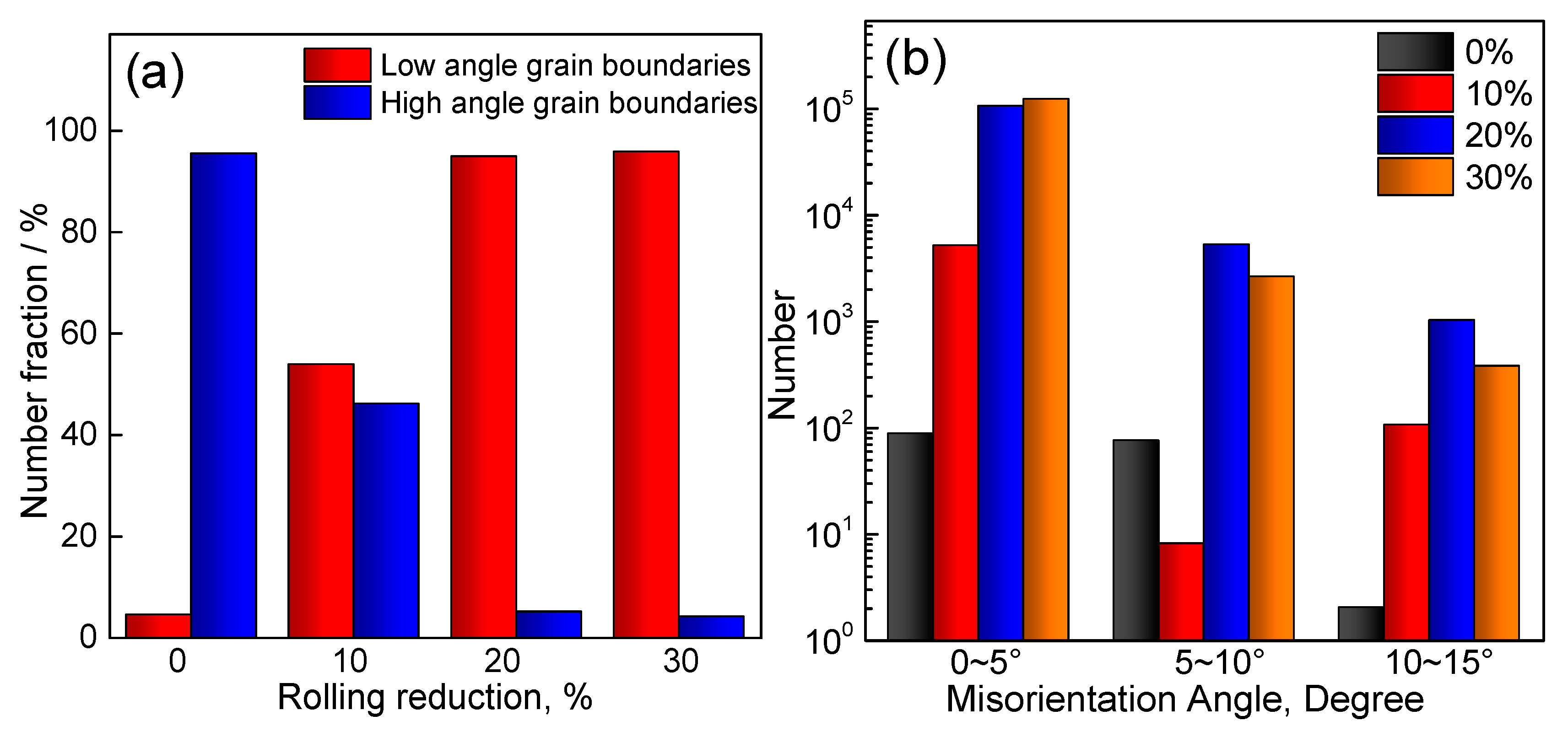
The grain boundary misorientation distribution over 0~15° corresponds to low-angle grain boundaries [26]. Figure 4a shows the statistical result for the grain orientation difference distribution ratio of copper under different rolling deformations. The proportion of high-angle grain boundaries in Coarse-grained copper reaches more than 90%, the proportion of low-angle grain boundaries in the copper sample gradually increased with the deformation in this study. The number of low-angle grain boundaries for different degrees of deformation is shown in Figure 4b.
3.3. Influence of Different Rolling Deformations on the Volta Potential of Copper
To explore how low-angle grain boundaries affect the Volta potential during the rolling process, EBSD tests were conducted to determine the microstructure of copper under different deformations and SKPFM tests were conducted in the area of interest to obtain the local Volta potential.
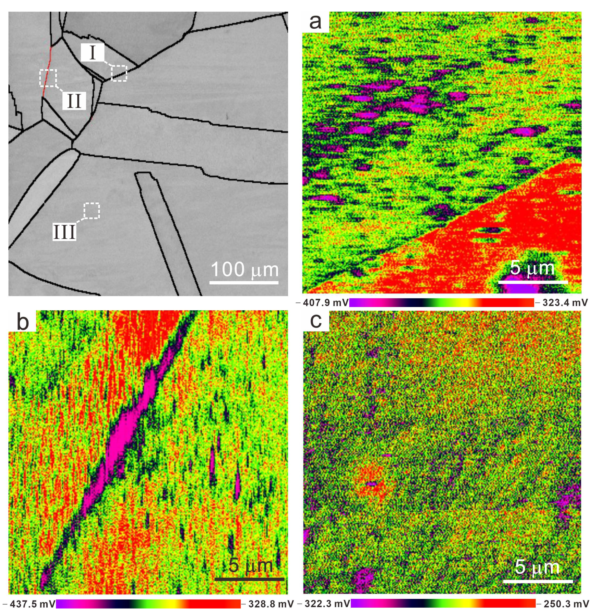
Figure 5 shows the low-angle grain boundary distribution (red lines) and the corresponding Volta potential maps of the undeformed copper sample. The regions marked with boxes I, II and III were selected for Volta potential scanning. Region I in Figure 5 contained a grain boundary. The Volta potential distribution was significantly different on the two sides of the high-angle grain boundaries. In Figure 3a, the Volta potential of the grain with a near (001) orientation in undeformed copper sample is lower than that with a near (111) orientation, whereas the Volta potential within each grain is basically the same. It is worth noting that there were several local low potential points within the grain, while these points were mainly caused by the existence of weeny metallurgical defects. Therefore, the potential difference can be attributed to the grain misorientation angle. Ma et al. [27] found that different misorientation angles change the Volta potential mainly because of the different atomic arrangements and spacing on different crystal surfaces, which leads to different electronic states on the surface of atoms.
Region II in Figure 5 contained a low-angle grain boundary. The Volta potentials between the two sub-grains were close to each other, which is consistent with the hypothesis that grain misorientation caused the Volta potential change. Interestingly, the Volta potential was noticeably show low value (less noble) along the low-angle grain boundary, in contrast with while on the high-angle grain boundaries, as shown in region I. This phenomenon shows that atoms near grain boundaries occupy different states as the grain boundary angle changes. For low-angle grain boundaries, the atomic lattices at the interface of grain boundaries are in the semi-coherent interface, which has been described within the classical Burgers and Bragg model [28] as being able to store distortion energy that increases with the angle of orientation within the range of the low-angle boundary. Therefore, lattice distortion at the semi-coherent interface expanded the atomic spacing to weaken the attraction of the nucleus to the outer layer electrons [18], i.e., the EWF decreased; hence, the Volta potential near the low-angle grain boundaries decreased. The grain boundaries at the high-angle grain boundaries are incoherent interfaces that do not induce lattice distortion; thus, the Volta potential did not cut down along the high-angle grain boundaries. Region III corresponded to the internal grain area. The Volta potential of untreated grains was relatively positive (more noble) and evenly distributed.
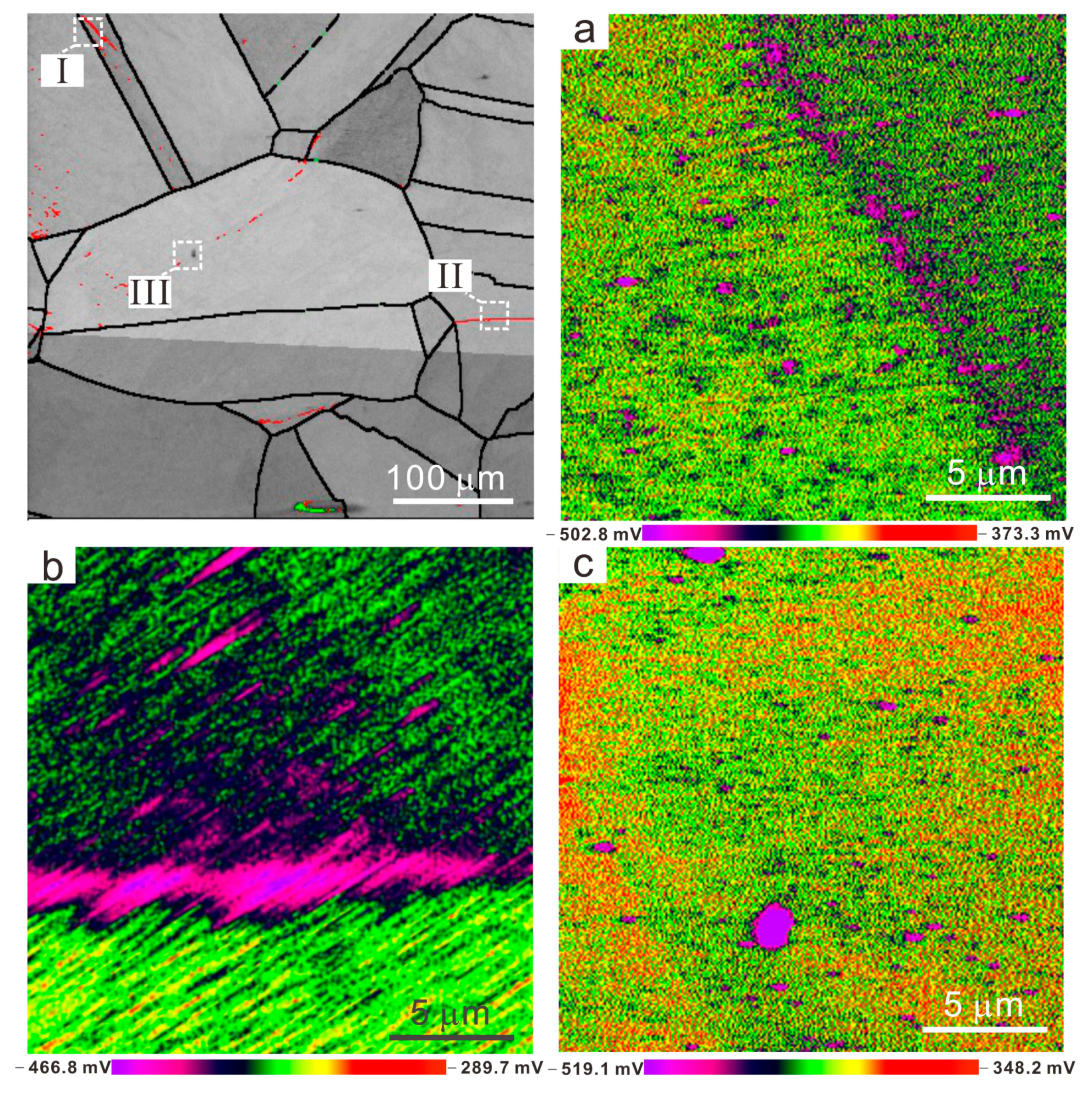
Figure 6 shows the low-angle grain boundary distribution and the corresponding Volta potential maps of the 10%-deformed copper sample. SKPFM was used to determine the low-angle grain boundary distribution. As shown in Figure 6a, the Volta potential reduce significantly in the area of low-angle grain boundary aggregation; Figure 6b presents a grain boundary region that is similar to Region II in Figure 5, there is a significant decrease in the potential at the low-angle grain boundaries. in Figure 6c, a few low-angle grain boundaries appeared inside the crystal, but local potential changes could still be detected by SKPFM.
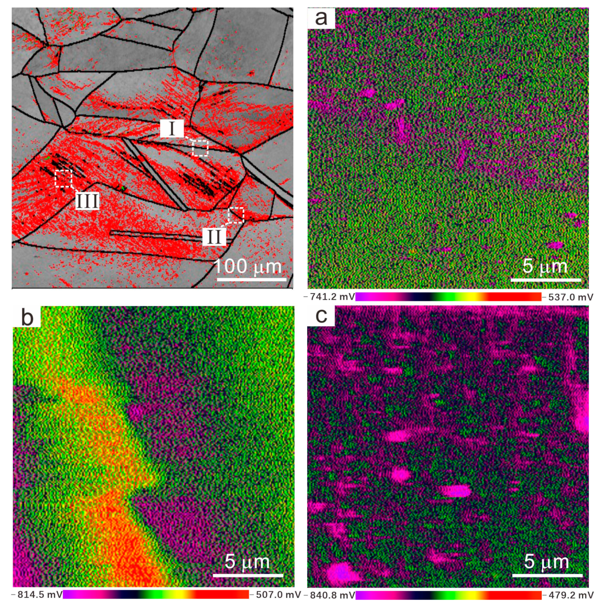
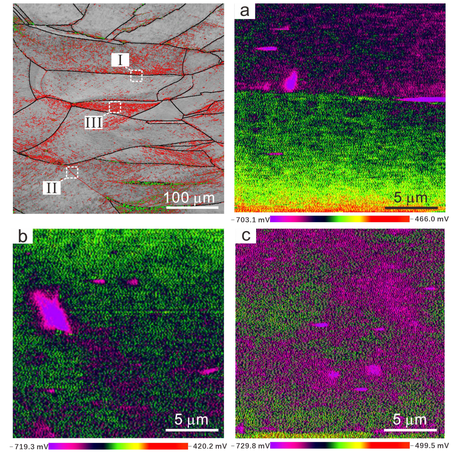
The Volta potential in the selected regions decline overall with increasing deformation [13]; Figure 7 and Figure 8 show the analysis of the copper surface potential for selected regions in samples with 20% and 30% deformation. Volta potential varied in the local areas, as shown in Figure 7a,b and Figure 8a,b, were directly caused by the difference of dislocation distribution. As shown in Figure 7c and Figure 8c, the entire interior of the grain was filled with the low angle grain boundaries and corresponding the low Volta potential value (less positive).
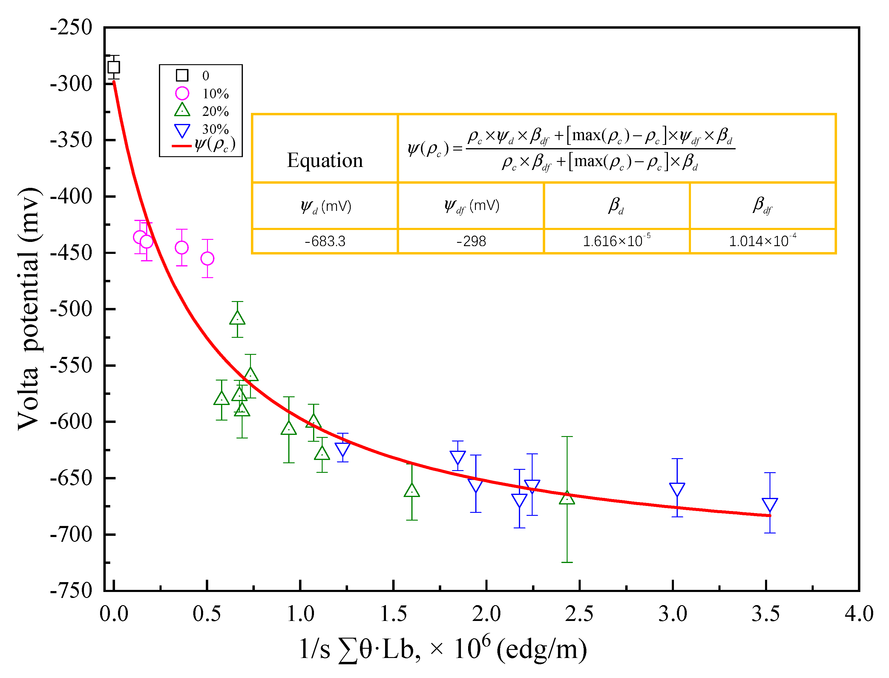
According to the principle of cold deformation in metals, the internal lattice of metal grains distort in response to plastic deformation, leading to the large generation and accumulation of dislocations. In principle, low-angle grain boundaries are formed by geometrically necessary dislocations (GNDs) [29,30]. Tan et al. proposed a method to calculate the dislocation density. The number of low-angle grain boundaries in the localized area is used to obtain the dislocation density ρc. The formula for ρc is , where S represents the grain area, Σθ represents the orientation difference cumulative of low-angle grain boundary, and Lb is the measured step size [31]. The dislocation density of a large number of local areas was statistically analyzed in selected EBSD microregions, and the geometric dislocation density of the selected region was correlated with the Volta potential, as shown in Figure 9. An increase in the dislocation density clearly causes a change in the Volta potential of the sample. The dislocation density ρc is almost linearly correlated with the Volta potential for dislocation densities below 1.5 × 10⁶ but increasing the dislocation density beyond 1.5 × 10⁶ does not produce a noticeable decrease in the Volta potential. That is, the Volta potential tends to be flat for dislocation densities above 1.5 × 10⁶. This result shows that the dislocation density is not linear in the Volta potential. In the discussion part, the reason why the volt potential does not decrease under the high dislocation density was analyzed.
4. Discussion
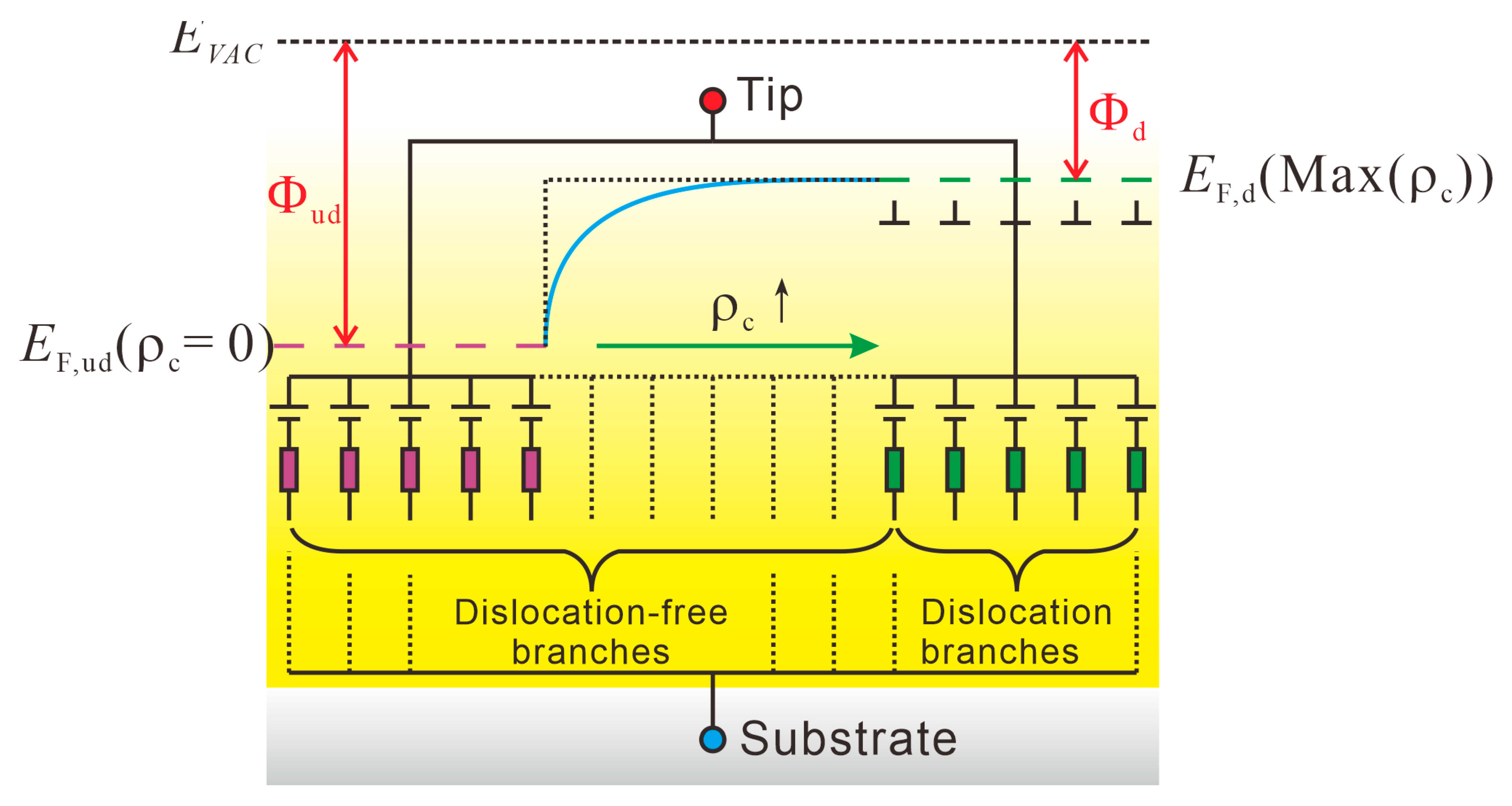
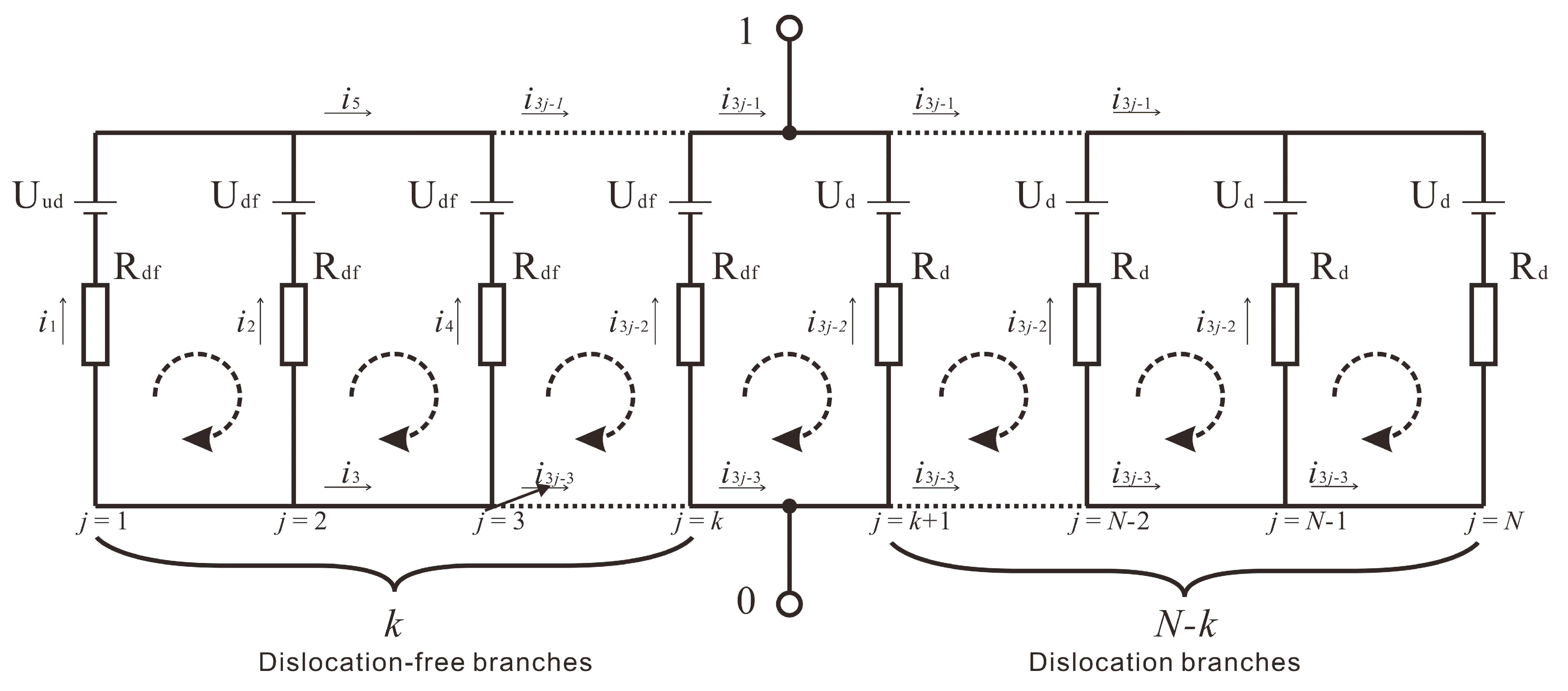
Wen Li et al. [32] proposed a theoretical model for the change in the EWF induced by a single dislocation for conventional polycrystalline copper: briefly, the lattice distortion induced by a dislocation weakens the electrostatic binding between the nucleus and the outermost electron, which increases the electron Fermi level and decreases the value of the electron escape function in the dislocation region. However, this model can only be used to explain how a single dislocation changes the Volta potential, and no literature is available to quantitatively correlate the dislocation density with the Volta potential or to explain why the Volta potential tends to flatten after large deformation. Therefore, a simplified circuit model based on energy band theory from solid state physics is proposed to describe the influence of the dislocation density on the Volta potential. The model is shown in Figure 10 and Figure 11.
The model is based on the following assumptions.
- 1.
- The effects of orientation differences of the low-angle grain boundaries on the Volta potential are neglected.
- 2.
- The SKPFM scanned area is divided into a dislocation aggregation area and an undeformed area, where electrons flow from the substrate to the tip. The electronic flow of the material is modelled as several parallel tunnels, which are divided into dislocation tunnels and perfect lattice tunnels. Deformed region containing high density of dislocation branches, while undeformed region containing dislocation- free branches. For a fixed probe collection area, increasing the dislocation density is equivalent to increasing the proportion of electrons flowing through the dislocation tunnel.
- 3.
- The circuit model shown in Figure 11 is constructed for convenience of calculation and analysis, where each parallel tunnel is modelled as a branch between the power supply element and the parallel circuits. Considering the physical meaning of the Fermi level shows that a high Fermi level facilitates electron escape. That is, a high Fermi level essentially increases the electromotive force of a branch. Hence, the intense of the voltage difference (Udf and Ud) is related to the Fermi level. The branch resistance (Rdf and Rd) depends on the resistance of electrons flowing through the parallel tunnel (the degree of lattice distortion). Finally, the calculated voltage U1-0 is expressed as the Volta potential from the tip to the substrate.
The assumptions presented above and the basic circuit diagram are used to determine the number of branches in terms of the node voltages from 0 to 1, as given below, and the detailed calculation is provided in the Appendix A:
where Ud and Rd represent the Volta potential Ψd (dislocation branch) and the internal resistance coefficient for electron escape βd (dislocation branch), respectively, under the condition of dislocation induced by deformation. Udf and Rdf represent the Volta potential Ψdf (dislocation-free branch) and internal resistance coefficient for electron escape βdf (dislocation-free branch). The node voltage for 0 to 1 U1-0 represents the Volta potential Ψ of the measured region. The total number of branches in the power supply is N, the number of Rdf branches is k and the number of Rd branches is N − k.
The voltage-resistance relationship given above can be used to derive an expression for the Volta potential Ψ1-0 in terms of the internal resistance.
Note that the value of Ψ1-0 depends on the proportion of k and N − k for a constant total number of branches. The ratio of the number of dislocation branches to the total number of branches is (, we set the dislocation density ρc for the (N k) and when severe plastic deformation occurs in the probe scanning area, the maximum dislocation density is defined as Max (ρc), all the branches in the parallel circuit model are basically dislocation branches, so Max () is the (N0). K is the Max (ρc) − (ρc). Through these Settings, the final formula for as a function of the calculated dislocation density ρc is given below.
Equation (4) was used to plot the Volta potential versus the dislocation density, as shown in Figure 10. At a high ρc, Ψ(ρc) → Ψd; whereas for ρc→ 0, Ψ(ρc) → Ψdf. This result shows that the Volta potential does not decrease linearly with the dislocation density but slowly approaches the potential extremum of the high dislocation density region beyond a specific dislocation density, where the magnitude of this extremum is determined by the limiting Fermi level of the dislocation pathway.
To verify the formula and model presented above, the calculated dislocation density ρc was substituted into Equation (4) and fitted to obtain the curve Ψ(ρc) shown in Figure 9. It is more appropriate to use the fitted values of Ψ(ρc) than the calculated values. Figure 9 shows that the circuit model is effective, and the geometrically necessary dislocation density affect the Volta potential electric potential. That is, there is a well-defined mapping between the Volta potential and dislocation density. For a constant dislocation density, the Volta potential decreases significantly with the dislocation density. However, the Volta potential peaks at a sufficiently high strain and then becomes insensitive to the dislocation density.
5. Conclusions
SKPFM is highly sensitive to changes in the Volta potential at grain boundaries and can be used to descriptive decrease in the Volta potential at low-angle grain boundaries induced by lattice distortion. A reasonable model and calculation formula were proposed in this study to quantitatively correlate the Volta potential and dislocation density. That is, the Volta potential decreases with the increase of the dislocation density. However, the Volta potential is not linear in the dislocation density. Beyond a threshold dislocation density, the decrease in the Volta potential with the dislocation density slows down and gradually approaches a limit value.
Author Contributions
Conceptualization, Y.Z. and W.S.; methodology, W.S.; software, Y.Z. and W.S.; validation, W.S. and S.X.; formal analysis, Y.Z. and W.S.; investigation, S.X.; resources, W.S. and S.X.; data curation, W.S. and Y.Z.; writing—original draft preparation, Y.Z.; writing—review and editing, W.S.; visualization, W.S.; supervision, S.X.; project administration, S.X.; funding acquisition, W.S. and S.X. All authors have read and agreed to the published version of the manuscript.
Funding
This research was funded by the National Natural Science Foundation of China (Grant No. 51801038,51774103,51974097), The Program of “One Hundred Talented People” of Guizhou Province (Grant No. 20164014), Guizhou Province Science and Technology Project (Grant No.[2018]5781,20191414,20192162,20192163).
Institutional Review Board Statement
Not applicable.
Informed Consent Statement
Informed consent was obtained from all subjects involved in the study.
Data Availability Statement
Data can be provided upon request.
Acknowledgments
The authors are indebted to National Natural Science Foundation of China (Grant Nos. 51801038,51774103,51974097), The Program of “One Hundred Talented People” of Guizhou Province (Grant No. 20164014), Guizhou Province Science and Technology Project (Grant No.[2018]5781,20191414,20192162,20192163).
Conflicts of Interest
The authors declared that they have no conflict of interest to this work. We declare that we do not have any commercial or associative interest that represents a conflict of interest in connection with the work submitted.
Appendix A
Figure 11 clearly shows that the key to improving the dislocation density is to increase the number of dislocation tunnels: when all the branches correspond to dislocations, the node voltage from 0 to 1 is exactly the same as for a dislocation for a single branch, whereas the node voltage is the same as that for a perfect crystal of 0 and 1 when all the branches correspond to a perfect lattice. Within this model, the key factor that changes the 0, 1 node is the ratio of the number of dislocation branches to the number of perfect lattice branches. When the ratio fluctuates between 0% and 100%, the dominant potential is measured at the 0 and 1 nodes.
A statistical analysis shows that the circuit diagram presented above has (2N − 4) independent nodes and (N − 1) loops. Kirchhoff Current Law and Kirchhoff voltage law can be applied to circuit to formulate the node current equation and the loop voltage equation, yielding analytical expressions of (3N − 6) branch currents are obtained [33].
As the circulation unit is controllable, the analytic calculation of the current of the multiple circuit can be completed using a symbolic operation function in MATLAB software. The procedure is illustrated using an example below.
Taking the fourth-order circuit as an example, if N = 5, then k = 3, corresponding to a branch with 3Rdf and 2Rd branches. According to Kirchhoff’s law, the fourth-order circuit has a total of 5 independent nodes and 4 loops, resulting in 9 equations.
Node current equation:
Loop voltage equation:
The inhomogeneous linear equations presented above can be used to determine the following coefficient matrix of the current variable and the augmented matrix of the solution.
Solving for the determinant of the matrix presented above yields i1:
The calculated current is used to obtain the voltage U1-0 at both ends of the loop for the fourth-order circuit.
The circuit matrix obtained for this multistage network shows that each order increases the current equation by 2 nodes at the same time; that is, the determinant repeats. The matrix can be indefinitely extended to determine the loop voltage U1-0 in terms of the numbers of escape electronic branches k and N − k at the ends as follows:
References
- Anantha, K.H.; Örnek, C.; Ejnermark, S.; Medvedeva, A.; Sjöström, J.; Pan, J. Correlative Microstructure Analysis and In Situ Corrosion Study of AISI 420 Martensitic Stainless Steel for Plastic Molding Applications. J. Electrochem. Soc. 2017, 164, C85–C93. [Google Scholar] [CrossRef]
- Rohwerder, M.; Turcu, F. High-resolution Kelvin probe microscopy in corrosion science: Scanning Kelvin probe force microscopy (SKPFM) versus classical scanning Kelvin probe (SKP). Electrochim. Acta 2007, 53, 016. [Google Scholar] [CrossRef]
- Schmutz, P.; Frankel, G.S. Corrosion Study of AA2024-T3 by Scanning Kelvin Probe Force Microscopy and In Situ Atomic Force Microscopy Scratching. J. Electrochem. Soc. 2019, 145, 105719. [Google Scholar] [CrossRef] [Green Version]
- Zhu, M.; Zhang, Q.; Yuan, Y.; Guo, S.; Huang, Y. Study on the correlation between passive film and AC corrosion behavior of 2507 super duplex stainless steel in simulated marine environment. J. Electroanal. Chem. 2020, 864, 114072. [Google Scholar] [CrossRef]
- Bettini, E.; Eriksson, T.; Boström, M.; Leygraf, C.; Pan, J. Influence of metal carbides on dissolution behavior of biomedical CoCrMo alloy: SEM, TEM and AFM studies. Electrochim. Acta 2011, 56, 9413–9419. [Google Scholar] [CrossRef]
- Örnek, C.; Leygraf, C.; Pan, J. On the Volta potential measured by SKPFM—fundamental and practical aspects with relevance to corrosion science. Corros. Eng. Sci. Technol. 2019, 54, 185–198. [Google Scholar] [CrossRef] [Green Version]
- Li, W.; Wang, Y.; Li, D.Y. Response of the electron work function to deformation and yielding behavior of copper under different stress states. Phys. Status Solidi A 2004, 201, 2005–2012. [Google Scholar] [CrossRef]
- Li, W.; Li, D.Y. Influence of surface morphology on corrosion and electronic behavior. Acta Mater. 2006, 54, 445–452. [Google Scholar] [CrossRef]
- Li, D.Y.; Li, W. Electron work function: A parameter sensitive to the adhesion behavior of crystallographic surfaces. Appl. Phys. Lett. 2001, 79, 4337. [Google Scholar] [CrossRef]
- Li, W.; Li, D.Y. Effect of surface geometrical configurations induced by microcracks on the electron work function. Acta Mater. 2005, 53, 3871–3878. [Google Scholar] [CrossRef]
- Li, W.; Li, D.Y. On the correlation between surface roughness and work function in copper. J. Chem. Phys. 2005, 122, 064708. [Google Scholar] [CrossRef]
- Xue, M.; Wang, W.; Wang, F.; Ou, J.; Li, C.; Li, W. Understanding of the correlation between work function and surface morphology of metals and alloys. J. Alloys Compd. 2013, 577, 1–5. [Google Scholar] [CrossRef]
- Sarvghad, M.; Muránsky, O.; Steinberg, T.A.; Hester, J.; Hill, M.R.; Will, G. On the effect of cold-rolling on the corrosion of SS316L alloy in a molten carbonate salt. Sol. Energy Mater. Sol. Cells 2019, 202, 110136. [Google Scholar] [CrossRef]
- Sadewasser, S.; Glatzel, T. Kelvin Probe Force Microscopy Measuring and Compensating Microscopy; Springer: Heidelberg, Germany, 2012. [Google Scholar]
- Örnek, C.; Engelberg, D.L. SKPFM measured Volta potential correlated with strain localisation in microstructure to understand corrosion susceptibility of cold-rolled grade 2205 duplex stainless steel. Corros. Sci. 2015, 99, 164–171. [Google Scholar] [CrossRef]
- Davoodi, A.; Esfahani, Z.; Sarvghad, M. Microstructure and corrosion characterization of the interfacial region in dissimilar friction stir welded AA5083 to AA7023. Corros. Sci. 2016, 107, 133–144. [Google Scholar] [CrossRef]
- Rahimi, E.; Rafsanjani-Abbasi, A.; Imani, A.; Hosseinpour, S.; Davoodi, A. Correlation of surface Volta potential with galvanic corrosion initiation sites in solid-state welded Ti-Cu bimetal using AFM-SKPFM. Corros. Sci. 2018, 140, 30–39. [Google Scholar] [CrossRef]
- Li, W.; Li, D.Y. Variations of work function and corrosion behaviors of deformed copper surfaces. Appl. Surf. Sci. 2005, 240, 388–395. [Google Scholar] [CrossRef]
- Ma, Z.; Xiong, X.; Chen, L.; Su, Y. Quantitative calibration of the relationship between Volta potential measured by scanning Kelvin probe force microscope (SKPFM) and hydrogen concentration. Electrochim. Acta. 2021, 366, 137422. [Google Scholar] [CrossRef]
- Sarvghad, M.; Chenu, T.; Will, G. Comparative interaction of cold-worked versus annealed inconel 601 with molten carbonate salt at 450 °C. Corros. Sci. 2017, 116, 88–97. [Google Scholar] [CrossRef]
- Cheng, T.; Shi, W.; Xiang, S.; Ballingerc, R.G. Volta potential mapping of the gradient strengthened layer in 20CrMnTi by using SKPFM. J. Mater. Sci. 2020, 55, 12403–12420. [Google Scholar] [CrossRef]
- Ni, L.; Chaofang, D.; Cheng, M.; Xiao, L.; Decheng, K.; Yucheng, J.; Min, A.; Jiangli, C.; Liang, Y.; Xiaoteng, L.; et al. Insight into the localized strain effect on micro-galvanic corrosion behavior in AA7075-T6 aluminum alloy. Corros. Sci. 2021, 180, 109174. [Google Scholar]
- Cheng, M.; Chaofang, D.; Li, W.; Decheng, K.; Xiaogang, L. Long-term corrosion kinetics and mechanism of magnesium alloy AZ31 exposed to a dry tropical desert environment. Corros. Sci. 2020, 163, 108274. [Google Scholar]
- Iannuzzi, M.; Vasanth, K.L.; Frankel, G.S. Unusual Correlation between SKPFM and Corrosion of Nickel Aluminum Bronzes. J. Electrochem. Soc. 2017, 164, C488–C497. [Google Scholar] [CrossRef] [Green Version]
- Zhang, J.; Xu, L.; Han, Y.; Zhao, L.; Xiao, B. New perspectives on the grain boundary misorientation angle dependent intergranular corrosion of polycrystalline nickel-based 625 alloy. Corros. Sci. 2020, 172, 108718. [Google Scholar] [CrossRef]
- Yejun, G.; Yang, X.; Srolovitz, D.J.; El-Awady, J.A. Self-healing of low angle grain boundaries by vacancy diffusion and dislocation climb. Scr. Mater. 2018, 155, 155–159. [Google Scholar]
- Aili, M.; Lianji, Z.; Dirk, E.; Qingmiao, H.; Shaokang, G.; Yugui, Z. Understanding crystallographic orientation dependent dissolution rates of 90Cu-10Ni alloy: New insights based on AFM/SKPFM measurements and coordination number/electronic structure calculations. Corros. Sci. 2020, 164, 108320. [Google Scholar]
- Mackenzie, J.K. A theory of sintering and the theoretical yield strength of solids. Ph.D. Thesis, Bristol University, Bristol, UK, 1949. [Google Scholar]
- Muñoz, J.A. Geometrically Necessary Dislocations (GNDs) in iron processed by Equal Channel Angular Pressing (ECAP). Mater. Lett. 2018, 238, 42–45. [Google Scholar] [CrossRef]
- Cui, L.; Jiang, S.; Xu, J.; Peng, R.L.; Mousavianb, R.Z.; Moverarea, J. Revealing relationships between microstructure and hardening nature of additively manufactured 316L stainless steel. Mater. Des. 2021, 198, 109385. [Google Scholar]
- Tan, Y.B.; Wang, X.M.; Ma, M.; Zhang, J.X.; Liu, W.C.; Fu, R.D.; Xiang, S. A study on microstructure and mechanical properties of AA 3003 aluminum alloy joints by underwater friction stir welding. Mater. Charact. 2017, 127, 41–52. [Google Scholar] [CrossRef]
- Li, L. Effects of dislocation on electron work function of metal surface. Mater. Sci. Technol. 2002, 18, 1057–1060. [Google Scholar] [CrossRef]
- Rahimi, M.; Soleymani, B.; Aminifar, F.; Gholami, A. A New Methodology for Circuit Analysis with Reverse Analysis Capability. J. Circuits Syst. Comput. 2017, 26, 1750101. [Google Scholar] [CrossRef]
Figure 1.
Effect of probe-sample distance on the Volta potential: (a) Volta potential is measured at different distances between the tip and Al (top) or Cu (bottom), (b) the continuous change in the Volta potential on the surface of Al or Cu at different distances from the samples to the tip.
Figure 1.
Effect of probe-sample distance on the Volta potential: (a) Volta potential is measured at different distances between the tip and Al (top) or Cu (bottom), (b) the continuous change in the Volta potential on the surface of Al or Cu at different distances from the samples to the tip.

Figure 2.
Metallographic images of copper with different degrees of deformation (ND stand for the normal direction, RD stand for the rolling direction): (a) undeformed, (b) 10%, (c) 20% and (d) 30%.
Figure 2.
Metallographic images of copper with different degrees of deformation (ND stand for the normal direction, RD stand for the rolling direction): (a) undeformed, (b) 10%, (c) 20% and (d) 30%.

Figure 3.
EBSD images of copper with different degrees of deformation: (a) undeformed, (b) 10%, (c) 20% and (d) 30%.
Figure 3.
EBSD images of copper with different degrees of deformation: (a) undeformed, (b) 10%, (c) 20% and (d) 30%.

Figure 4.
Grain boundary orientation statistics at different deformations: (a) distribution statistics of the grain boundary orientation difference under different deformations and (b) quantitative analysis of low grain boundaries at different angles.
Figure 4.
Grain boundary orientation statistics at different deformations: (a) distribution statistics of the grain boundary orientation difference under different deformations and (b) quantitative analysis of low grain boundaries at different angles.

Figure 5.
The low-angle grain boundary distribution of undeformed copper and the Volta potential for the selected regions. In the EBSD image of undeformed copper. The Volta potential of regions I, II and III with different grain boundary distribution were measured to obtain the corresponding potential distribution maps (a), (b) and (c).

Figure 6.
The low-angle grain boundary distribution and the Volta potential of the selected regions Figure 10. deformation. In the EBSD image of 10% deformed copper. The Volta potential of regions I, II and III with different grain boundary distribution were measured to obtain the corresponding potential distribution maps (a), (b) and (c).

Figure 7.
The low-angle grain boundary distribution and the Volta potential of the selected regions for a copper sample with 20% deformation. In the EBSD image of 20% deformed copper. The Volta potential of regions I, II and III with different grain boundary distribution were measured to obtain the corresponding potential distribution maps (a), (b) and (c).

Figure 8.
The low-angle grain boundary distribution and the Volta potential of the selected regions for a copper sample with 30% deformation. In the EBSD image of 30% deformed copper. The Volta potential of regions I, II and III with different grain boundary distribution were measured to obtain the corresponding potential distribution maps (a), (b) and (c).

Figure 9.
Numerically calculated Volta potential as a function of the dislocation density, the dislocation density and Volta potential of different regions of copper cross-sections with different deformations were selected for statistics, and the curve represents the fitting result of the formula Ψ(ρc). Ψ(ρc) is derived from the discussion section.

Figure 10.
The schematic diagram of energy band concerning the relationship between Fermi levels and the dislocation density, Ef,ud (ρc = 0) stand for the Fermi level of undeformed grains, Ef,d (Max (ρc)) stand for the Fermi level of deformed grains, (Φd) stand for Work function of deformed grains (Φud) stand for work function of undeformed grains, ρc stand for the dislocation density.

Figure 11.
A simplified electrical model for the tip measuring area, Udf stands for the voltage difference of dislocation -free branches, Ud stands for the voltage difference of dislocation branches. Rdf stands for the resistance of electrons flowing through the dislocation -free branches, Rd stands for the resistance of electrons flowing through the dislocation branches, i stands for the branch current, k stands for the number of dislocation -free branches, N stands for the number of the surface of the grain branches.

Publisher’s Note: MDPI stays neutral with regard to jurisdictional claims in published maps and institutional affiliations. |
© 2021 by the authors. Licensee MDPI, Basel, Switzerland. This article is an open access article distributed under the terms and conditions of the Creative Commons Attribution (CC BY) license (https://creativecommons.org/licenses/by/4.0/).
Share and Cite
MDPI and ACS Style
Zhang, Y.; Shi, W.; Xiang, S. Using SKPFM to Determine the Influence of Deformation-Induced Dislocations on the Volta Potential of Copper. Metals 2021, 11, 1166. https://0-doi-org.brum.beds.ac.uk/10.3390/met11081166
AMA Style
Zhang Y, Shi W, Xiang S. Using SKPFM to Determine the Influence of Deformation-Induced Dislocations on the Volta Potential of Copper. Metals. 2021; 11(8):1166. https://0-doi-org.brum.beds.ac.uk/10.3390/met11081166
Chicago/Turabian StyleZhang, Yang, Wei Shi, and Song Xiang. 2021. "Using SKPFM to Determine the Influence of Deformation-Induced Dislocations on the Volta Potential of Copper" Metals 11, no. 8: 1166. https://0-doi-org.brum.beds.ac.uk/10.3390/met11081166
Note that from the first issue of 2016, this journal uses article numbers instead of page numbers. See further details here.