Article

Periodic Relief Fabrication and Reversible Phase Transitions in Amorphous Ge2Sb2Te5 Thin Films upon Multi-Pulse Femtosecond Irradiation

1
Faculty of Physics, Lomonosov Moscow State University (MSU), 1/2 Leninskie Gory, 119991 Moscow, Russia
2
Big Data Storage and Analysis Center, Lomonosov MSU, 27/1 Lomonosovsky Avenue, 119192 Moscow, Russia
3
Skobeltsyn Institute of Nuclear Physics, Lomonosov MSU, 1/2 Leninskie Gory, 119991 Moscow, Russia
4
Quantum Technology Center, Lomonosov MSU, 1/35 Leninskie Gory, 119991 Moscow, Russia
5
Institute of Advanced Materials and Technologies, National Research University of Electronic Technology, 1 Shokina Sq., 124498 Zelenograd, Russia
6
Moscow Institute of Physics and Technology, 9 Institutskiy Per., 141701 Dolgoprudny, Russia
7
Kurnakov Institute of General and Inorganic Chemistry of the Russian Academy of Sciences, 31 Leninsky Avenue, 119991 Moscow, Russia
8
National Research Institute “Kurchatov Institute”, 1 Akademika Kurchatova Square, 123182 Moscow, Russia
*
Author to whom correspondence should be addressed.
Submission received: 29 December 2021 / Revised: 14 January 2022 / Accepted: 17 January 2022 / Published: 20 January 2022
(This article belongs to the Section Microscale Materials Science)

Abstract

:
Ge2Sb2Te5 based devices attract the attention of researchers due to wide opportunities in designing phase change memory. Herein, we studied a possibility to fabricate periodic micro- and nanorelief at surfaces of Ge2Sb2Te5 thin films on silicon oxide/silicon substrates under multi-pulse femtosecond laser irradiation with the wavelength of 1250 nm. One-dimensional lattices with periods of 1250 ± 90 and 130 ± 30 nm were obtained depending on the number of acted laser pulses. Emergence of these structures can be explained by plasmon-polariton generation and laser-induced hydrodynamic instabilities, respectively. Additionally, formation of the lattices whose spatial period is close to the impacted laser wavelength can be modelled by considering the free carrier contribution under intensive photoexcitation. Raman spectroscopy revealed both crystallization and re-amorphization of the irradiated films. The obtained results show a possibility to fabricate rewritable all-dielectric data-storage devices based on Ge2Sb2Te5 with the periodic relief.

1. Introduction

Chalcogenide alloy Ge2Sb2Te5 (GST225) is well-known as a basic material for non-volatile and rewritable memory applications (DVD-RW or Blu-Ray) [1], as well as reconfigurable nanophotonic devices [2]. This medium exhibits a large difference between the optical or electrical properties of the amorphous and crystalline states. Usually, rapid and reversible phase switching is achieved under optical pumping [3] or resistive heating [4], which allows for the design of so-called phase change memory devices.
In the case of femtosecond laser treatment, the rate and energy efficiency of triggered crystallization [5,6,7] and amorphization [8,9,10] might be increased up to several times compared with the impact by nanosecond or longer laser pulses. This increase is usually explained by the non-thermal nature of melting and quenching processes precisely at the femtosecond laser treatment [11,12]. Under such consideration features and kinetics of the phase transitions depend on the GST225 film thickness and substrate type [7].
An additional feature of femtosecond laser treatment of GST225 and other semiconductors, as well as metals and dielectrics, is the formation of anisotropic laser-induced periodic surface structures (LIPSS or “ripples”) [13,14,15,16]. The period of these one-dimensional lattices is comparable with or less than the wavelength of incident radiation. The ripples formation is caused by photoexcitation of surface electromagnetic waves (SEW) or scattering of evanescent waves [17]. Formed structures induce giant birefringence and dichroism [18], as well as anisotropy of electrical properties of irradiated material [19]. These LIPSS promise wide applications in polarization optics [18,20] and photovoltaics [19,21]. Additionally, the presence of periodic modulation on the surface or inside the bulk of the material opens new prospects on data storage [18,22,23] when several bits can be written within one anisotropically nanostructured voxel. In this case, data storage and subsequent encoding in the same voxel are achieved by direct laser writing of LIPSS with appropriate orientations and optical birefringence values [24]. Furthermore, laser-induced gratings can be used as antireflective [25] and hydrophobic [26] coatings for solar cells.
Previously, LIPSS with the wavelength period were fabricated on amorphous GST225 thin films deposited on conductive substrates [14,15,16]. In addition, it was revealed that the treatment by near-infrared femtosecond pulses facilitates the effective penetration of radiation into the used material, which exhibits relatively small absorbance and reflection in this spectral range [27]. However, any quantitative explanation of ripple formation in these films has not been made yet.
In the present paper, we perform and theoretically analyse experiments on multi-pulse femtosecond laser irradiation, which lead to LIPPS fabrication, as well as direct and reversible phase transitions in amorphous as-deposited GST225 thin films. An oxidized monocrystalline silicon wafer was chosen in our experiments as a base substrate to demonstrate the possibility of ripples formation on all-dielectric samples and easy integration of contemporary planar silicon technologies.

2. Materials and Methods

2.1. Samples and Experimental Techniques

Amorphous GST225 films with a thickness of 130 nm were deposited by direct current (DC) magnetron sputtering of a crystalline target (ACI alloys) on thermally oxidized crystalline silicon substrates. The residual pressure in the chamber before the deposition was 3 × 10⁻³ Pa, and the pressure of Ar during the process was 5.7 × 10⁻¹ Pa. The sputtering power was 100 W. The thickness, composition, and structure of the fabricated films were controlled by atomic force microscopy (AFM), as well as Auger electron spectrometry and X-ray diffraction analysis, respectively [28].
The samples were irradiated by femtosecond laser pulses with an Avesta laser system [29,30] in air (central wavelength λ = 1250 nm, repetition rate ν = 10 Hz, pulse duration τ = 135 fs, fluence F = 0.1 J/cm2). The pulses were linearly polarized, and the beam incident angle was normal (Figure 1a). The scanning mode during processing was realized by moving the films in the horizontal plane along a meandering trajectory (Figure 1b) at a scanning rate from 2 to 500 μm/s (Table 1).
Each treated track with the length of 0.5 mm was scanned along the Y-axis by a focused laser beam with 150 μm in diameter (D). The number of overlapping laser spots Ns was determined by the following equation:
Ns = νD/V,
where ν is the laser pulse repetition rate, and V is the scanning rate. Therefore, the resulting value of Ns varied from 3 to 750 (Table 1).
The images and profiles of modified areas were obtained by the scanning electron microscope (SEM, Carl Zeiss Supra 40) and AFM (NT-MDT SolverPro), respectively. The phase composition was analyzed by Raman spectroscopy using a Horiba Jobin Yvon HR800 spectrometer with He–Ne laser excitation source (633 nm), Olympus MPlan N objective with a 100× lens, numerical aperture of 0.9 and waist of 1 μm in diameter. The used Raman edge filter cut-off was 100 cm−1. The Raman spectra accumulation times were 5 s and the accumulation number for each spectrum was 10, respectively. We chose the excitation power of 0.1 mW, which provided the reproducibility of repeated measurements at the same area, and correlated well with the simple estimation proposed in this paper [31].

2.2. Theoretical Simulation of Surface Photoexcitation and LIPSS Formation

The period of LIPSS might be comparable with the wavelength of acted laser pulses or sufficiently smaller than them. In the first case, these structures are called low-spatial-frequency LIPSS (LSFL), while in the second case—they are called high-spatial-frequency LIPSS (HSFL) [13]. The occurrence of one or the other type of LIPSS depends on both the parameters of laser pulses (polarization, fluence, and pulse number) and the relation between ε1 and ε2—dielectric permittivities of ambient medium and irradiated material, respectively. Therefore, both factors must be analyzed to explain the fabrication of LIPSS in our experiments, as described below.
The femtosecond-assisted fabrication of one-dimensional LIPSS oriented perpendicularly to the incident radiation polarization and with a period close to the wavelength of the incident radiation is usually described by surface plasmon-polaritons (SPPs) generation caused by intensive photoexcitation [17,32,33]. The conditions of this excitation at the near-surface layer between two media are:
ε1 > 0, Re ε2 < 0, |Re ε2| > ε1,
where ε1 = 1 denotes the air dielectric permittivity, and the negative real part of ε2 corresponds to the photoexcited near-surface layer of GST225 during irradiation.
Initially, without laser irradiation, the dielectric permittivity ε2 of the semiconductor is positive. Under femtosecond laser irradiation, this value decreases according to the Drude model. The photoinduced free charge carriers provide the following contribution to the value of the dielectric permittivity:
ε 2 ( ω ) = ε 4 π n e e 0 2 m * ω ( ω + i γ ) ,
where ω is the incident laser radiation frequency, γ = e0/(m*μ) is the carrier collision frequency, e0 and m* are the electron charge and effective mass, respectively, as well as μ = 52 cm2/(V∙s) is the charge carrier mobility for GST225 [34]. The static dielectric permittivity of ε   = 18.2 and ε   = 44.2 correspond [27] to the non-excited amorphous and crystalline GST225, respectively. In this case, ne is the value of non-equilibrium charge carrier density, which can be estimated from the following differential equation:
d n e d t α ( 1 R ) I ( t ) ћ ω γ n e ,
where the absorption and reflection constants of the amorphous GST225 thin films for the wavelength of 1250 nm are taken as α = 24,500 cm−1 and R = 0.39 [27], respectively.
Laser pulse intensity I(t) is defined as follows [35]:
I ( t ) = I 0 · t · e x p ( 4 t τ ) ,   I ( t ) d t = F .
where t is the time, while τ and F are the laser pulse duration and the fluence, respectively.
In our work, to calculate the orientation and period of LIPSS we use the hybrid model initially suggested by professor Sipe et al. [36] and later modified by Bonse J et al. (so-called “Sipe–Drude theory”) [37]. This approach utilizes the so-called efficacy factor η(kx,ky), which is the probability of ripples formation with the spatial period Λ and the specific direction x or y in the sample surface plane. In our calculations, the surface wave vector k with the projections kx and ky onto the irradiated surface is normalized to the incident radiation wavelength λ:
|k| = λ/Λ.
For the linear polarization as well as the irradiation parameters and specific materials, the calculation of the efficacy factor η(kx,ky) is provided by the next set of Equations (7)–(18) joined with Equations (3)–(5):
η ( k x , k y ) = 2 π | v ( k + ) + v * ( k ) | ,
where
v ( k ± ) = [ h s s ( k ± ) ( k ± · y ) 2 + h k k ( k ± ) ( k ± · x ) 2 ] γ t | t s ( k i ) | ,
( k ± · y ) = ( sin θ ± k y ) k ± ,
( k ± · x ) = k x k ± ,
k ± = k x 2 + ( sin θ + k y ) 2 ,
h s s ( k ± ) = 2 i 1 k ± 2 + ε ˜ k ± 2 ,
h k k ( k ± ) = 2 i ( ε 2 k ± 2 ) ( 1 k ± 2 ) ε ˜ 1 k ± 2 + ε 2 k ± 2 0 ,
t s ( k i ) = 2 | cos θ | | cos θ | + ε 2 ( sin θ ) 2 ,
γ t = ε ˜ 1 4 π { 1 + ( 1 f ) ( ε 2 1 ) [ F ( s ) R × G ( s ) ] / 2 } ,
R = ε 2 1 ε 2 + 1 ,
F ( s ) = s 2 + 1 s ,
G ( s ) = s 2 + 4 + s 2 s 2 + 1 .
Here, ε 2 is the complex dielectric permittivity value for the irradiated material, which depends on the free charge carrier concentration, according to Equation (3). The two roughness parameters–shape factor s and filling factor f encode the topological characteristics of the surface [37]. The standard values of s = 0.4 and f = 0.1 correspond to surfaces with spherically shaped islands acting as scattering centers for the incident optical radiation [17]. The laser polarization is oriented along the Y-axis on the distribution map for η(kx,ky).

3. Results and Discussion

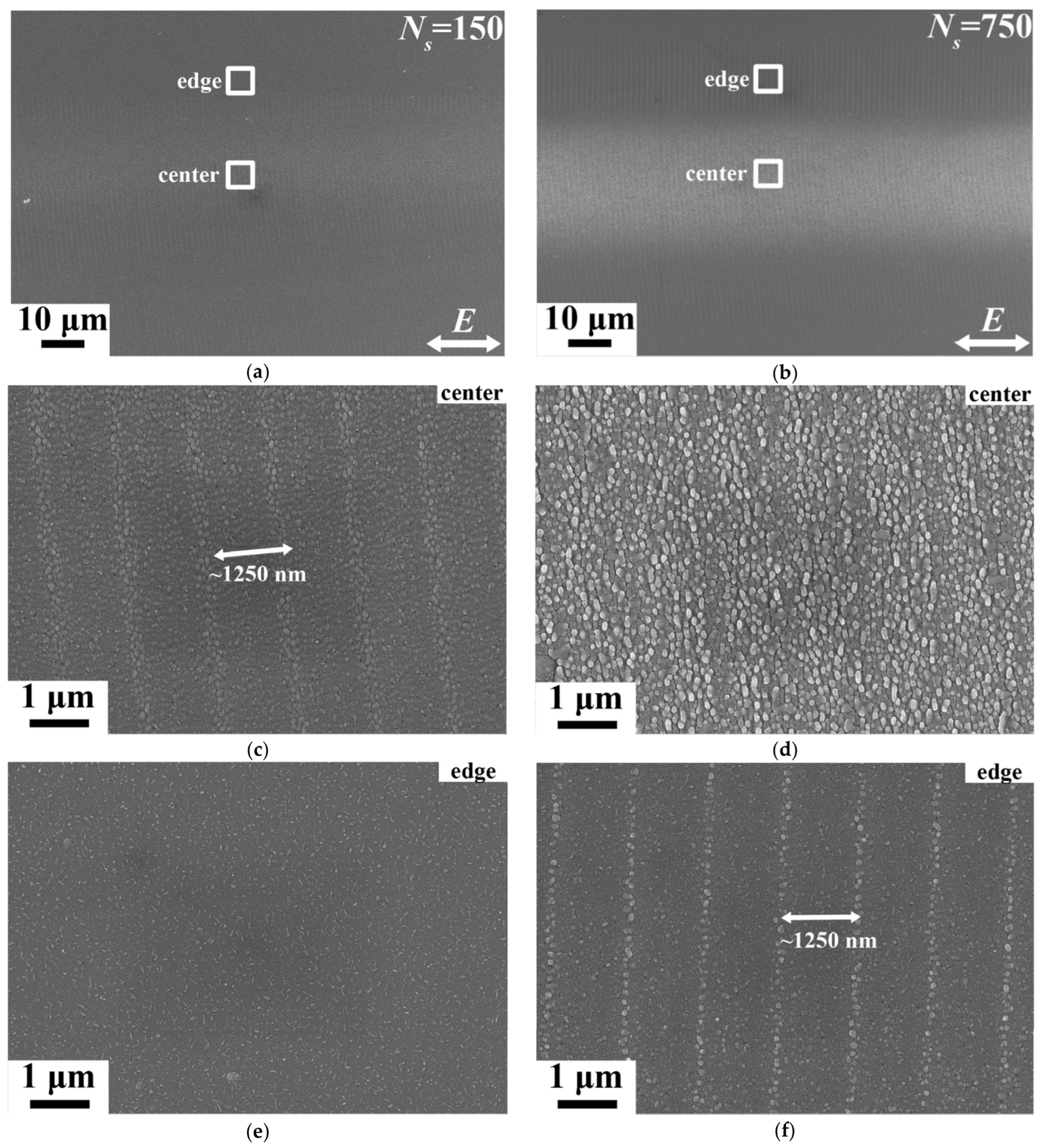
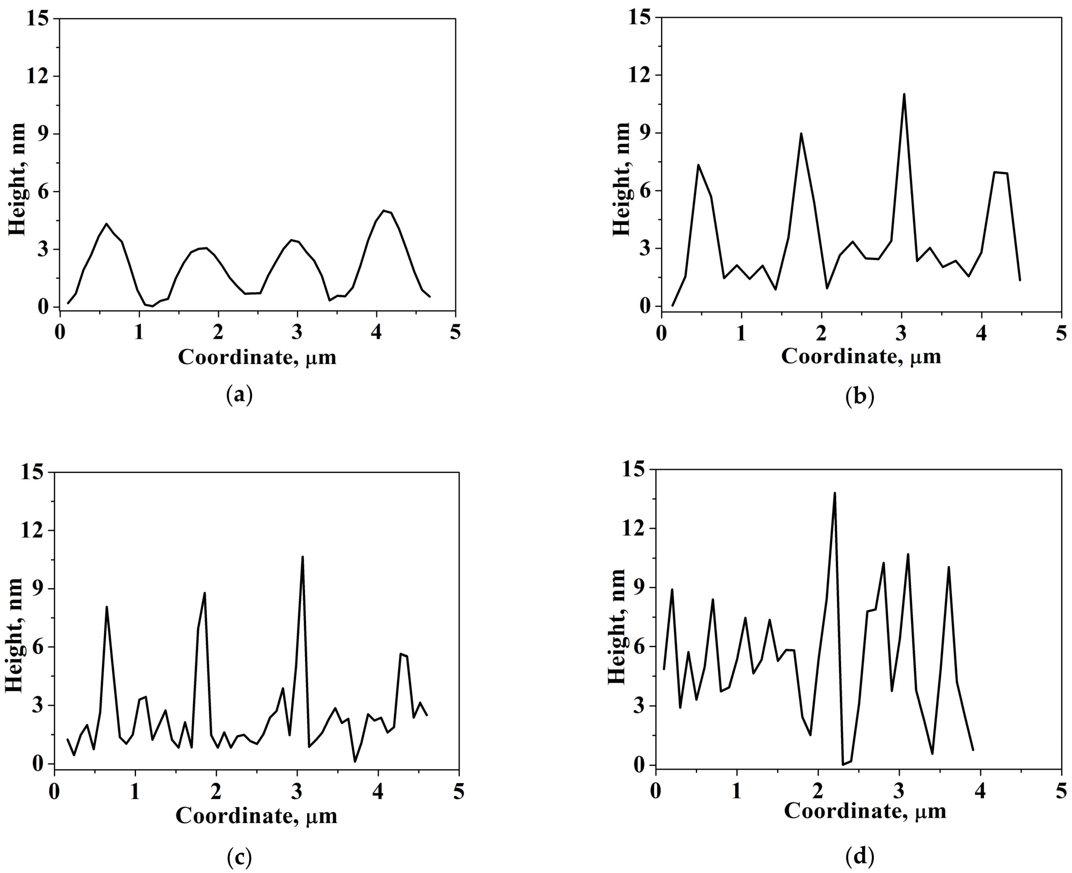
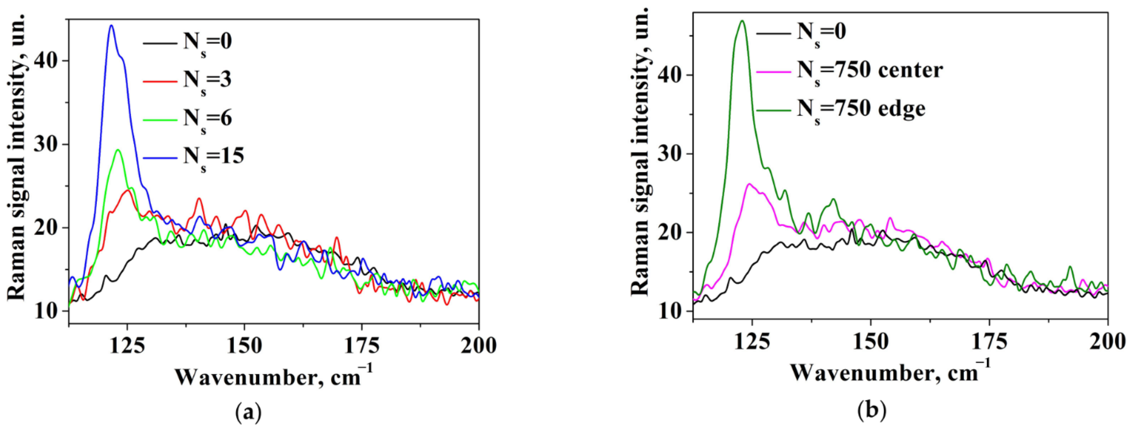
3.1. Structural Properties

LIPSS formation was revealed on the irradiated GST225 surface starting with the overlapping pulses number Ns = 150. The gratings formed at these conditions are directed orthogonally to the laser polarization and represent grain ridges with the period Λ = 1250 ± 90 nm, which is close to the incident laser radiation wavelength (Figure 2a–c,f). The ripples absent at edges of femtosecond laser beam spots where a local fluence of the laser beam with a spatial gaussian profile is low to modify surface (Figure 2e). The height (H) of the formed ripples increases from 4 ± 1 to 9 ± 2 nm with rising Ns values (Figure 3a–c). This growth of the LIPSS height is caused by the feedback between laser pulse absorption, scattering, and surface modification during irradiation [38]. These gratings may be classified as LSFL [13]. In addition, their structural properties may indicate SPPs generation during the intensive photoexcitation of free charge carriers [17,32,33].
When the pulse number exceeded Ns = 300, an additional type of LIPSS was observed appearing at the center (Figure 2b) of the irradiated area. It represents elongated clusters possessing a subwavelength period of Λ = 130 ± 30 nm (Figure 2d) and height of H = 9 ± 3 nm (Figure 3d), and thus can be defined as HSFL. Moreover, these clusters are directed perpendicularly to the polarization of the laser pulses. The formation of this HSFL is generally explained by laser-induced hydrodynamic instabilities associated with Marangoni convection and similar thermo-capillary effects, which manifest themselves at the times that exceed the laser pulse duration [17,39]. Additionally, it was previously shown that the multi-pulse treatment leads to the growth of scattering efficiency during surface modification [17,38]. Consequently, this increases the light absorption and heat of the surface, which causes stronger manifestation of the hydrodynamic instabilities.
The Raman spectrum of the amorphous GST225 thin film (Ns = 0) demonstrates the asymmetric broadband from 110 to 200 cm−1 with the maximum near 145 cm−1 (Figure 4a). The wide band is explained by the short-range crystallographic order for the amorphous phase [40]. In turn, the maximum at 145 cm−1 corresponds to the hexagonal Sb2Te3 mode [41].
With regards to an area corresponding to the edge of the incident femtosecond laser beam spots, the following changes after laser irradiation can be seen from the evolution of the obtained Raman spectra (Figure 4a). With the Ns increasing from 3 to 15, the intensity of the peak near 125 cm−1 grows in comparison with the rest of the spectrum. The peak value near 125 cm−1 in this band is associated with the GeTe4−nGen (n = 1, 2) tetrahedra mode [40] and indicates the transition to the face-centered cubic (FCC) crystalline structure [42]. The intensity of the peak near 125 cm−1 strongly depends on the state of the phase [43]. Therefore, it might be assumed that the observed behavior is related to the appearance and increase of the crystalline fraction in GST225 [7]. The crystallization can be described by the simultaneous volume and surface nucleation processes [44].
In the case of Ns = 750, the Raman spectra showed that the intensity ratio of the 125 cm−1 line to the 110–200 cm−1 broadband maximum is smaller in the laser spot center than at the periphery area (Figure 4b). This behavior may indicate a possible re-amorphization occurring in the film exposed by the larger number of overlapping laser pulses. This reversible phase transition is possible in GST225 due to the metastability of its FCC crystalline lattice [45,46]. In the case of laser action on the GST225 film surface, the FCC phase transformation into the amorphous one can probably be achieved during the subsequent processes of material melting due to the strong light absorption of crystalline GST225 (α ≈ 2 × 105 cm−1 for the λ = 1250 nm) [27] and subsequent rapid quenching of the melt [47]. In this case, the rapid cooling of the film, which is necessary for the amorphous phase formation can be provided by the efficient heat removal to the substrate [48,49].

3.2. Modelling of LIPSS Formation

To satisfy the conditions (2) for SPPs generation in amorphous GST225, the free charge carrier concentration should be larger than the threshold value, calculated as ne0 = 4 × 1019 cm−3 from (3). The actual average free charge carrier concentration estimated for radiation parameters by (4) and (5) is ne = 1022 cm−3 and exceeds the threshold. Sipe−Drude calculations provided the dielectric permittivity as ε2 = −7.6 + 2.9i for the last value. The corresponding efficacy factor η(kx,ky) achieves the local maxima if the surface wave vector projections satisfy the following conditions: |kx| = 0 and |ky| = 1.05 (Figure 5). The obtained result corresponds to the formation of ripples with the period near Λ = 1200 nm and the orientation orthogonal to the laser polarization. Structural properties of the predicted LIPSS are consistent with features of experimentally observed surface gratings. Therefore, this confirms the hypothesis regarding the SPPs generation mechanism of the LSFL formation for the used radiation parameters [17,37].
Of note, the HSFL formation effect probably has a cumulative nature [38], as it starts occurring with the number of laser pulses above Ns = 300. The formation of HSFL with a period of about 130 nm can probably have an hydrodynamic mechanism (see Section 3.1), outside of the Sipe−Drude and SPPs generation model. In this case, for future studies, we will need to use other theoretical approaches and consider the time interval after the end of the laser pulse [17,39]. Namely, relaxation of electron gas to lattice at the times longer than the laser pulse duration may induce the thermal expansion of melted material and, consequently, its extrusion and deformation. However, if the melt viscosity is insufficient, the surface tension could inhibit this process. Therefore, the resulting relief may depend on whether the modulation on the surface of the melt can be maintained by its viscosity until solidification. Additionally, cracks formation during the cooling of the film may affect HSFL formation.
The experiments also demonstrated that the formation of HSFL, as a rule, accompanied the observed re-amorphization, which, as mentioned above, can be provided by rapid solidification of the melt after exposure to a laser pulse. Therefore, both of these processes are probably based on a common mechanism, which is associated with the fact that the solidification rate in this case may be high enough to both preserve the liquid surface modulation and provide the rapid transition of the melt into the amorphous phase, in the absence of long-range order in the atomic structure.

4. Conclusions

In conclusion, we observed the formation of two types of LIPSS during the femtosecond laser treatment of amorphous GST225 thin films on dielectric substrates at the incident radiation wavelength of λ = 1250 nm. The first type of gratings, whose spatial period is close to the laser wavelength, can be induced by the SPPs excitation. This suggestion is confirmed by the Sipe−Drude theory calculations. The structures of the second type have a spatial period noticeably shorter than the laser wavelength and may be explained by the hydrodynamic instabilities in the laser-induced melt and solidification at the times longer than the laser pulse duration, when the cooling rate is sufficiently fast to preserve modulations that emerge at the near surface melt. An additional confirmation of this process is the reversible phase transition of GST225 observed under the same femtosecond laser radiation processing conditions, when the crystallization of amorphous GST225 is replaced by its re-amorphization. The latter can be explained by the rapid solidification of the melt due to the effective heat dissipation into the substrate.
The observed results seem promising for the design of all-dielectric phase change memory devices based on GST225, where one can realize a reversible phase transition and anisotropic relief modulation simultaneously. The periodic relief may ensure artificial anisotropy, which makes these structures sensitive to the polarization of incident light and the direction of applied current in the plane of a sample.

Author Contributions

Conceptualization, S.K. and P.K.; methodology, S.Z. and D.S.; software, A.K. and D.S.; validation, A.K., D.P., T.K. (Tatiana Kaminskaya), P.L., V.G. and T.K. (Tatiana Kunkel); formal analysis, A.K. and T.K. (Tatiana Kunkel); investigation, A.K., D.P. and T.K. (Tatiana Kaminskaya), P.L., V.G. and T.K. (Tatiana Kunkel); resources, P.L. and S.K.; data curation, A.K.; writing—original draft preparation, A.K.; writing—review and editing, S.Z., D.S., P.L., T.K. (Tatiana Kunkel) and S.K.; visualization, A.K.; supervision, S.K. and P.K.; project administration, S.Z. and P.L. All authors have read and agreed to the published version of the manuscript.

Funding

SEM: AFM, Raman spectroscopy studies, and calculations of the irradiated GST225 films were supported by the Russian Foundation for Basic Research (grant no. 20-32-90111). P. Lazarenko gratefully acknowledges a partial support for sample fabrication from the Russian Foundation for Basic Research (grant no. 20-07-01092). The initial amorphous GST225 films were fabricated at Core Facilities centers “MEMS and electronic components”, National Research University of Electronic Technology. An upgrade of the experimental setup for multi-pulse processing was made in frames of the National Technology Initiative in “Big Data Storage and Analysis Center”, Lomonosov MSU (contract of Ministry of Science and Higher Education of RF no. 7/1251/2019 on 15 August 2019).

Institutional Review Board Statement

Not applicable.

Informed Consent Statement

Not applicable.

Data Availability Statement

The data used in this research are available from the corresponding author upon reasonable request.

Acknowledgments

The authors wish to acknowledge Leonid Golovan and Mikhail Smayev for fruitful discussions.

Conflicts of Interest

The authors declare no conflict of interest.

References

  1. Guo, P.; Sarangan, A.M.; Agha, I. A Review of Germanium-Antimony-Telluride Phase Change Materials for Non-Volatile Memories and Optical Modulators. Appl. Sci. 2019, 9, 530. [Google Scholar] [CrossRef] [Green Version]
  2. Shi, X.; Chen, C.; Liu, S.; Li, G. Nonvolatile, Reconfigurable and Narrowband Mid-Infrared Filter Based on Surface Lattice Resonance in Phase-Change Ge2Sb2Te5. Nanomaterials 2020, 10, 2530. [Google Scholar] [CrossRef]
  3. Wuttig, M.; Yamada, N. Phase-change materials for rewriteable data storage. Nat. Mater. 2007, 6, 824–832. [Google Scholar] [CrossRef]
  4. Sun, X.; Roß, U.; Gerlach, J.W.; Lotnyk, A.; Rauschenbach, B. Nanoscale Bipolar Electrical Switching of Ge2Sb2Te5 Phase-Change Material Thin Films. Adv. Electron. Mater. 2017, 3, 3. [Google Scholar] [CrossRef]
  5. Sun, X.; Ehrhardt, M.; Lotnyk, A.; Lorenz, P.; Thelander, E.; Gerlach, J.W.; Smausz, T.; Decker, U.; Rauschenbach, B. Crystallization of Ge2Sb2Te5 thin films by nano- and femtosecond single laser pulse irradiation. Sci. Rep. 2016, 6, 28246. [Google Scholar] [CrossRef]
  6. Liu, Y.; Aziz, M.M.; Shalini, A.; Wright, C.D.; Hicken, R.J. Crystallization of Ge2Sb2Te5 films by amplified femtosecond optical pulses. J. Appl. Phys. 2012, 112, 123526. [Google Scholar] [CrossRef] [Green Version]
  7. Kunkel, T.; Vorobyov, Y.; Smayev, M.; Lazarenko, P.; Veretennikov, V.; Sigaev, V.; Kozyukhin, S. Experimental observation of two-stage crystallization of Ge2Sb2Te5 amorphous thin films under the influence of a pulsed laser. J. Alloys Compd. 2021, 851, 156924. [Google Scholar] [CrossRef]
  8. Siegel, J.; Gawelda, W.; Puerto, D.; Dorronsoro, C.; Solis, J.; Afonso, C.N.; DE Sande, J.C.G.; Bez, R.; Pirovano, A.; Wiemer, C. Amorphization dynamics of Ge2Sb2Te5 films upon nano- and femtosecond laser pulse irradiation. J. Appl. Phys. 2008, 103, 023516. [Google Scholar] [CrossRef] [Green Version]
  9. Hada, M.; Oba, W.; Kuwahara, M.; Katayama, I.; Saiki, T.; Takeda, J.; Nakamura, K.G. Ultrafast time-resolved electron diffraction revealing the nonthermal dynamics of near-UV photoexcitation-induced amorphization in Ge2Sb2Te5. Sci. Rep. 2015, 5, 13530. [Google Scholar] [CrossRef] [PubMed] [Green Version]
  10. Wang, Y.H.; Liu, F.R. Observation of the femtosecond laser-induced ultrafast amorphization in Ge2Sb2Te5 films by dynamics spectrum. J. Phys. Conf. Ser. 2020, 1676, 012161. [Google Scholar] [CrossRef]
  11. Ionin, A.A.; Kudryashov, S.I.; Samokhin, A. Material surface ablation produced by ultrashort laser pulses. Uspekhi Fizicheskih Nauk. 2017, 187, 159–172. [Google Scholar] [CrossRef]
  12. Inogamov, N.A.; Petrov, Y.V.; Khokhlov, V.A.; Zhakhovskii, V.V. Laser Ablation: Physical Concepts and Applications (Review). High Temp. 2020, 58, 632–646. [Google Scholar] [CrossRef]
  13. Bonse, J.; Kruger, J.; Höhm, S.; Rosenfeld, A. Femtosecond laser-induced periodic surface structures. J. Laser Appl. 2012, 24, 042006. [Google Scholar] [CrossRef]
  14. Kozyukhin, S.; Lazarenko, P.; Vorobyov, Y.; Baranchikov, A.; Glukhenkaya, V.; Smayev, M.; Sherchenkov, A.; Sybina, Y.; Polohin, A.; Sigaev, V. Laser-induced modification and formation of periodic surface structures (ripples) of amorphous GST225 phase change materials. Opt. Laser Technol. 2019, 113, 87–94. [Google Scholar] [CrossRef]
  15. Kozyukhin, S.; Smayev, M.; Sigaev, V.; Vorobyov, Y.; Zaytseva, Y.; Sherchenkov, A.; Lazarenko, P. Specific Features of Formation of Laser-Induced Periodic Surface Structures on Ge2Sb2Te5 Amorphous Thin Films under Illumination by Femtosecond Laser Pulses. Phys. Status Solidi 2020, 257, 257. [Google Scholar] [CrossRef]
  16. Kolchin, A.V.; Shuleiko, D.V.; Zabotnov, S.V.; Golovan, L.A.; Presnov, D.E.; Kaminskaya, T.P.; Lazarenko, P.I.; Kozyukhin, S.A.; Kashkarov, P.K. Formation of periodic surface structures in multilayer amorphous Ge2Sb2Te5 thin films irradiated by femtosecond laser pulses. J. Phys. Conf. Ser. 2020, 1686, 012006. [Google Scholar] [CrossRef]
  17. Bonse, J.; Gräf, S. Maxwell Meets Marangoni—A Review of Theories on Laser-Induced Periodic Surface Structures. Laser Photon. Rev. 2020, 14, 2000215. [Google Scholar] [CrossRef]
  18. Drevinskas, R.; Beresna, M.; Gecevičius, M.; Khenkin, M.; Kazanskii, A.G.; Matulaitienė, I.; Niaura, G.; Konkov, O.I.; Terukov, E.I.; Svirko, Y.P.; et al. Giant birefringence and dichroism induced by ultrafast laser pulses in hydrogenated amorphous silicon. Appl. Phys. Lett. 2015, 106, 171106. [Google Scholar] [CrossRef]
  19. Shuleiko, D.; Martyshov, M.; Amasev, D.; Presnov, D.; Zabotnov, S.; Golovan, L.; Kazanskii, A.; Kashkarov, P. Fabricating Femtosecond Laser-Induced Periodic Surface Structures with Electrophysical Anisotropy on Amorphous Silicon. Nanomaterials 2020, 11, 42. [Google Scholar] [CrossRef]
  20. Skoulas, E.; Tasolamprou, A.C.; Kenanakis, G.; Stratakis, E. Laser induced periodic surface structures as polarizing optical elements. Appl. Surf. Sci. 2021, 541, 148470. [Google Scholar] [CrossRef]
  21. Amasev, D.V.; Khenkin, M.V.; Drevinskas, R.; Kazansky, P.; Kazanskii, A.G. Anisotropy of optical, electrical, and photoelectrical properties of amorphous hydrogenated silicon films modified by femtosecond laser irradiation. Tech. Phys. 2017, 62, 925–929. [Google Scholar] [CrossRef]
  22. Lipatiev, A.S.; Fedotov, S.S.; Okhrimchuk, A.G.; Lotarev, S.V.; Vasetsky, A.M.; Stepko, A.A.; Shakhgildyan, G.Y.; Piyanzina, K.I.; Glebov, I.S.; Sigaev, V.N. Multilevel data writing in nanoporous glass by a few femtosecond laser pulses. Appl. Opt. 2018, 57, 978–982. [Google Scholar] [CrossRef] [PubMed]
  23. Fedotov, S.; Lipatiev, A.; Presniakov, M.; Shakhgildyan, G.; Okhrimchuk, A.; Lotarev, S.; Sigaev, V.N. Laser-induced cavities with controllable shape in nanoporous glass. Opt. Lett. 2020, 45, 5424–5427. [Google Scholar] [CrossRef] [PubMed]
  24. Lotarev, S.V.; Fedotov, S.S.; Kurina, A.I.; Lipatiev, A.S.; Sigaev, V.N. Ultrafast laser-induced nanogratings in sodium germanate glasses. Opt. Lett. 2019, 44, 1564–1567. [Google Scholar] [CrossRef] [PubMed]
  25. Dostovalov, A.; Bronnikov, K.; Korolkov, V.; Babin, S.; Mitsai, E.; Mironenko, A.; Tutov, M.; Zhang, D.; Sugioka, K.; Maksimovic, J.; et al. Hierarchical anti-reflective laser-induced periodic surface structures (LIPSSs) on amorphous Si films for sensing applications. Nanoscale 2020, 12, 13431–13441. [Google Scholar] [CrossRef]
  26. Varlamova, O.; Reif, J.; Stolz, M.; Borcia, R.; Borcia, I.D.; Bestehorn, M. Wetting properties of LIPSS structured silicon surfaces. Eur. Phys. J. B 2019, 92, 91. [Google Scholar] [CrossRef]
  27. Lazarenko, P.I.; Vorobyov, Y.V.; Fedyanina, M.E.; Sherchenkov, A.A.; Kozyukhin, S.; Yakubov, A.O.; Kukin, A.; Sybina, Y.S.; Sagunova, I.V. Peculiarities of Estimating the Optical Band Gap of Thin Films of Phase Change Memory Materials. Inorg. Mater. Appl. Res. 2020, 11, 330–337. [Google Scholar] [CrossRef]
  28. Gutwirth, J.; Wagner, T.; Bezdicka, P.; Hrdlička, M.; Vlček, M.; Frumar, M. On angle resolved RF magnetron sputtering of Ge–Sb–Te thin films. J. Non-Cryst. Solids 2009, 355, 1935–1938. [Google Scholar] [CrossRef]
  29. Agranat, M.B.; Ashitkov, S.I.; Ivanov, A.A.; Konyashchenko, A.V.; Ovchinnikov, A.V.; Podshivalov, A.A. Gigawatt Cr:forsterite regenerative amplifier of femtosecond pulses with a pulse repetition rate of 10 Hz. Quantum Electron. 2004, 34, 1018–1022. [Google Scholar] [CrossRef]
  30. Gordienko, V.M.; Ivanov, A.A.; Podshivalov, A.A.; Savel’Ev, A.B.; Rakov, E.V. Generation of superintense femtosecond pulses by the Cr:forsterite laser system. Laser Phys. 2006, 16, 427–435. [Google Scholar] [CrossRef]
  31. Andrikopoulos, K.S.; Yannopoulos, S.N.; Voyiatzis, G.A.; Kolobov, A.V.; Ribes, M.; Tominaga, J. Raman scattering study of the a-GeTe structure and possible mechanism for the amorphous to crystal transition. J. Phys. Condens. Matter 2006, 18, 965–979. [Google Scholar] [CrossRef] [Green Version]
  32. Emel’Yanov, V.I.; Zemskov, E.M.; Seminogov, V.N. Theory of formation of surface gratings under the action of laser radiation on surfaces of metals, semiconductors, and insulators. Sov. J. Quantum Electron. 1983, 13, 1556–1561. [Google Scholar] [CrossRef]
  33. Emel’Yanov, V.I.; Zemskov, E.M.; Seminogov, V.N. Theory of the formation of "normal" and "anomalous" gratings on the surfaces of absorbing condensed media exposed to laser radiation. Sov. J. Quantum Electron. 1984, 14, 1515–1521. [Google Scholar] [CrossRef]
  34. Shelimova, L.E.; Karpinskii, O.G.; Konstantinov, P.P.; Kretova, M.A.; Avilov, E.S.; Zemskov, V.S. Composition and Properties of Layered Compounds in the GeTe–Sb2Te3System. Inorg. Mater. 2001, 37, 342–348. [Google Scholar] [CrossRef]
  35. Dyukin, R.V.; Martsinovskiĭ, G.A.; Shandybina, G.D.; Yakovlev, E.B. Electrophysical phenomena accompanying femtosecond impacts of laser radiation on semiconductors. J. Opt. Technol. 2011, 78, 88–92. [Google Scholar] [CrossRef]
  36. Sipe, J.E.; Young, J.F.; Preston, J.; Van Driel, H.M. Laser-induced periodic surface structure. I. Theory. Phys. Rev. B 1983, 27, 1141–1154. [Google Scholar] [CrossRef]
  37. Bonse, J.; Rosenfeld, A.; Krüger, J. On the role of surface plasmon polaritons in the formation of laser-induced periodic surface structures upon irradiation of silicon by femtosecond-laser pulses. J. Appl. Phys. 2009, 106, 104910. [Google Scholar] [CrossRef]
  38. Bonse, J.; Rosenfeld, A.; Krüger, J. Implications of transient changes of optical and surface properties of solids during femtosecond laser pulse irradiation to the formation of laser-induced periodic surface structures. Appl. Surf. Sci. 2011, 257, 5420–5423. [Google Scholar] [CrossRef]
  39. Libenson, M.N. Laser-Induced Optical and Thermal Processes in Condensed Media and Their Mutual Influence; Nauka: Saint-Petersburg, Russia, 2007; p. 219. [Google Scholar]
  40. Němec, P.; Nazabal, V.; Moreac, A.; Gutwirth, J.; Beneš, L.; Frumar, M. Amorphous and crystallized Ge–Sb–Te thin films deposited by pulsed laser: Local structure using Raman scattering spectroscopy. Mater. Chem. Phys. 2012, 136, 935–941. [Google Scholar] [CrossRef]
  41. Xu, Z.; Chen, C.; Wang, Z.; Wu, K.; Chong, H.; Ye, H. Optical constants acquisition and phase change properties of Ge2Sb2Te5 thin films based on spectroscopy. RSC Adv. 2018, 8, 21040–21046. [Google Scholar] [CrossRef] [Green Version]
  42. Yin, Q.; Chen, L. Microstructure and crystallization kinetics of Ge2Sb2Te5–Sn phase change materials. J. Mater. Sci. Mater. Electron. 2018, 29, 16523–16533. [Google Scholar] [CrossRef]
  43. Kozyukhin, S.; Veres, M.; Nguyen, H.; Ingram, A.; Kudoyarova, V. Structural Changes in Doped Ge2Sb2Te5 Thin Films Studied by Raman Spectroscopy. Phys. Procedia 2013, 44, 82–90. [Google Scholar] [CrossRef] [Green Version]
  44. Vorobyov, Y.; Lazarenko, P.; Sherchenkov, A.; Vishnyakov, N.; Ermachikhin, A.; Kozyukhin, S. Kinetics of volume and surface driven crystallization in thin films. J. Phys. Condens. Matter 2020, 32, 355401. [Google Scholar] [CrossRef] [PubMed]
  45. Yamada, N.; Ohno, E.; Nishiuchi, K.; Akahira, N.; Takao, M. Rapid-phase transitions of GeTe-Sb2Te3pseudobinary amorphous thin films for an optical disk memory. J. Appl. Phys. 1991, 69, 2849–2856. [Google Scholar] [CrossRef]
  46. Bogoslovskiy, N.A.; Tsendin, K.D. Physics of switching and memory effects in chalcogenide glassy semiconductors. Semiconductors 2012, 46, 559–590. [Google Scholar] [CrossRef]
  47. Huang, H.; Zuo, F.; Zhai, F.; Wang, Y.; Lai, T.; Wu, Y.; Gan, F. Fast phase transition process of Ge2Sb2Te5 film induced by picosecond laser pulses with identical fluences. J. Appl. Phys. 2009, 106, 63501. [Google Scholar] [CrossRef]
  48. Siegel, J.; Schropp, A.; Solis, J.; Afonso, C.N.; Wuttig, M. Rewritable phase-change optical recording in Ge2Sb2Te5 films induced by picosecond laser pulses. Appl. Phys. Lett. 2004, 84, 2250–2252. [Google Scholar] [CrossRef] [Green Version]
  49. Møller, S.H.; Eriksen, E.H.; Tønning, P.L.; Jensen, P.B.; Chevallier, J.; Balling, P. Femtosecond-laser-induced modifications of Ge2Sb2Te5 thin films: Permanent optical change without amorphization. Appl. Surf. Sci. 2019, 476, 221–231. [Google Scholar] [CrossRef]
Figure 1. The scheme of multi-pulse processing of amorphous GST225 thin films on dielectric substrates by femtosecond laser irradiation (a). The scanning mode of femtosecond laser treatment (b).
Micro 02 00005 g001
Figure 2. SEM images of areas irradiated by Ns = 150 (a,c,e) and Ns = 750 (b,d,f).
Micro 02 00005 g002
Figure 3. AFM profiles of LIPSS obtained after irradiation by Ns = 150 (a), Ns = 300 (b), and Ns = 750 (c,d).
Micro 02 00005 g003
Figure 4. Raman spectra of initial samples (Ns = 0) and edges of treated area at the overlapping spots from Ns = 3 to Ns = 15 (a). Raman spectra of initial samples (Ns = 0), central and edge (at the distance of 50 μm from the center) regions of treated area at Ns = 750 (b). The maximum at 145 cm−1 was chosen for normalization.
Micro 02 00005 g004
Figure 5. Results of Sipe−Drude theory calculations for used radiation parameters in the provided experiment.
Micro 02 00005 g005
Table 1. The scan speed and the number of overlapping laser spots used for modification of amorphous GST225 thin films.
SampleScan Speed, μm/sNumber of Overlapping Laser Spots
15003
22506
310015
45030
52560
610150
75300
82750
Publisher’s Note: MDPI stays neutral with regard to jurisdictional claims in published maps and institutional affiliations.

