Role of Graphene in Constructing Multilayer Plasmonic SERS Substrate with Graphene/AgNPs as Chemical Mechanism—Electromagnetic Mechanism Unit

 and
and 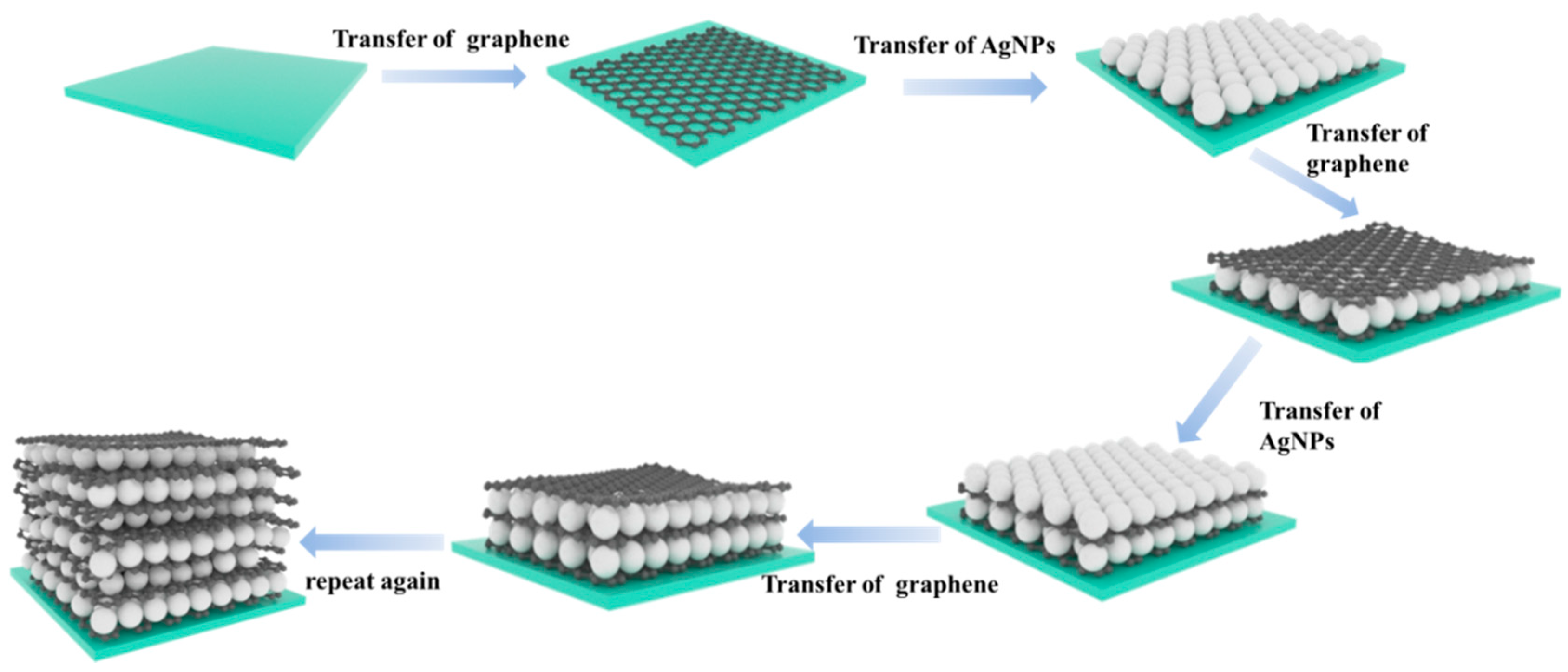
Abstract
:1. Introduction
2. Experiment
2.1. Materials and Instruments
2.2. Preparation of the SERS Substrate with Different CM–EM Units
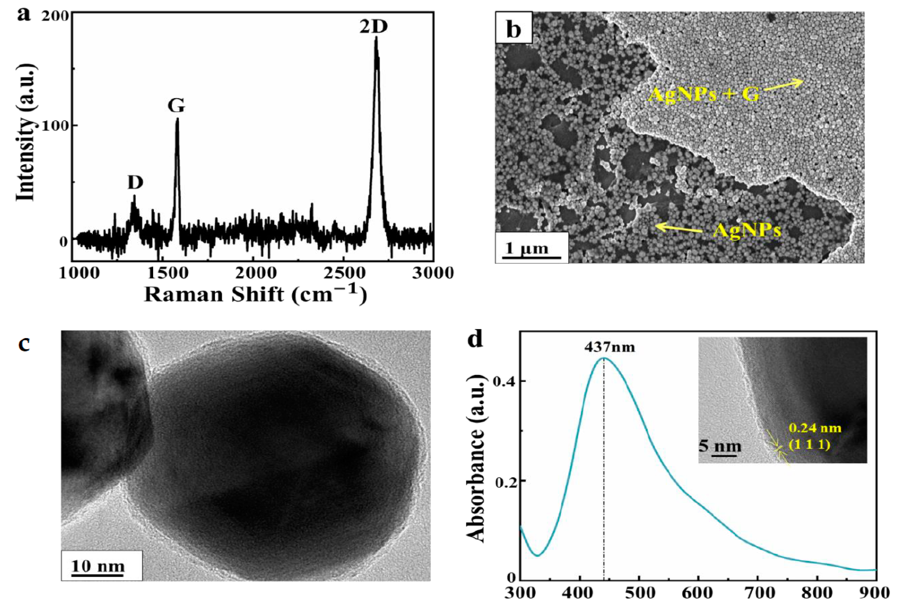
2.3. Characterization
2.4. FDTD Simulations
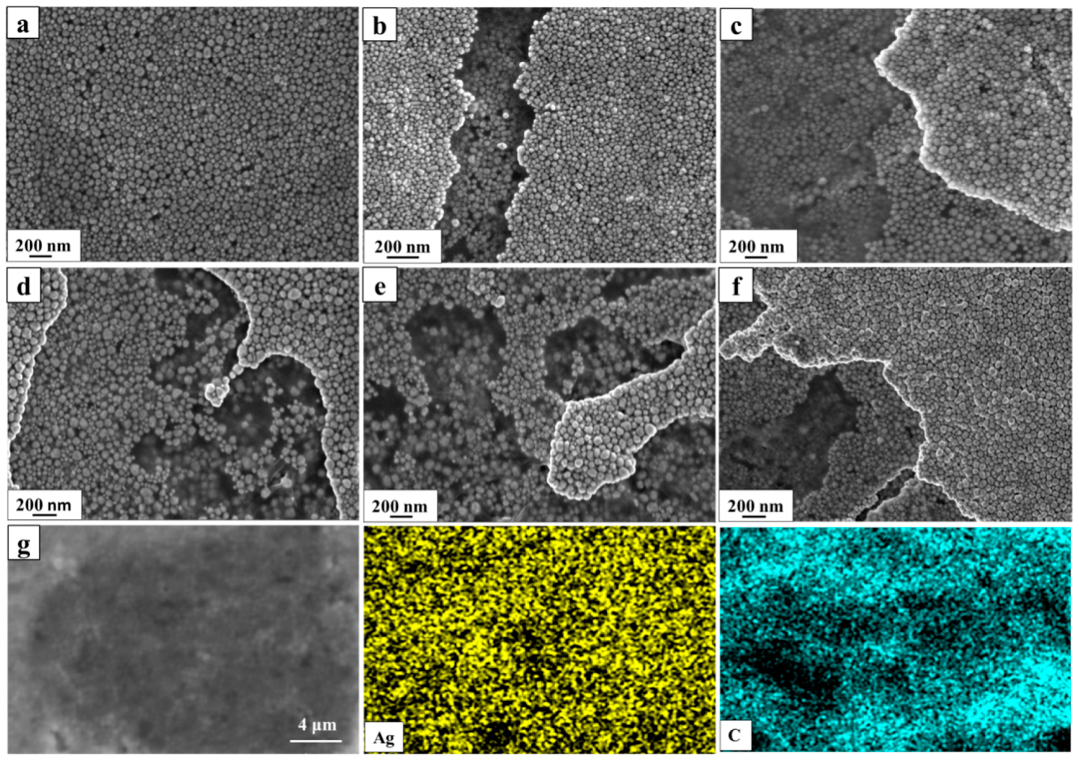
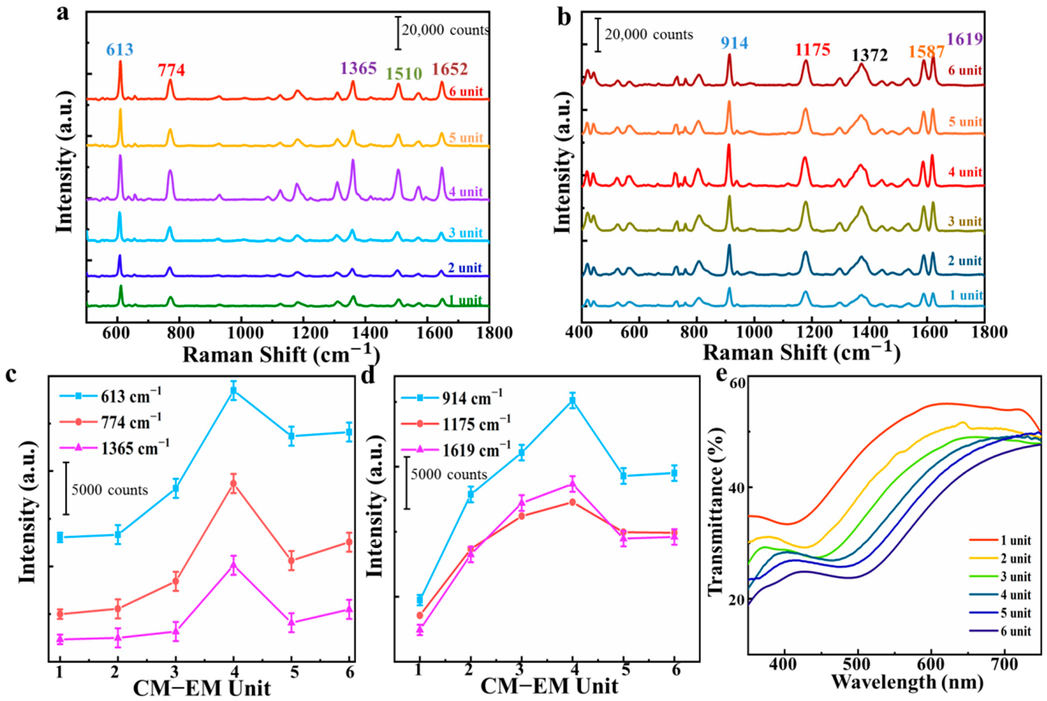
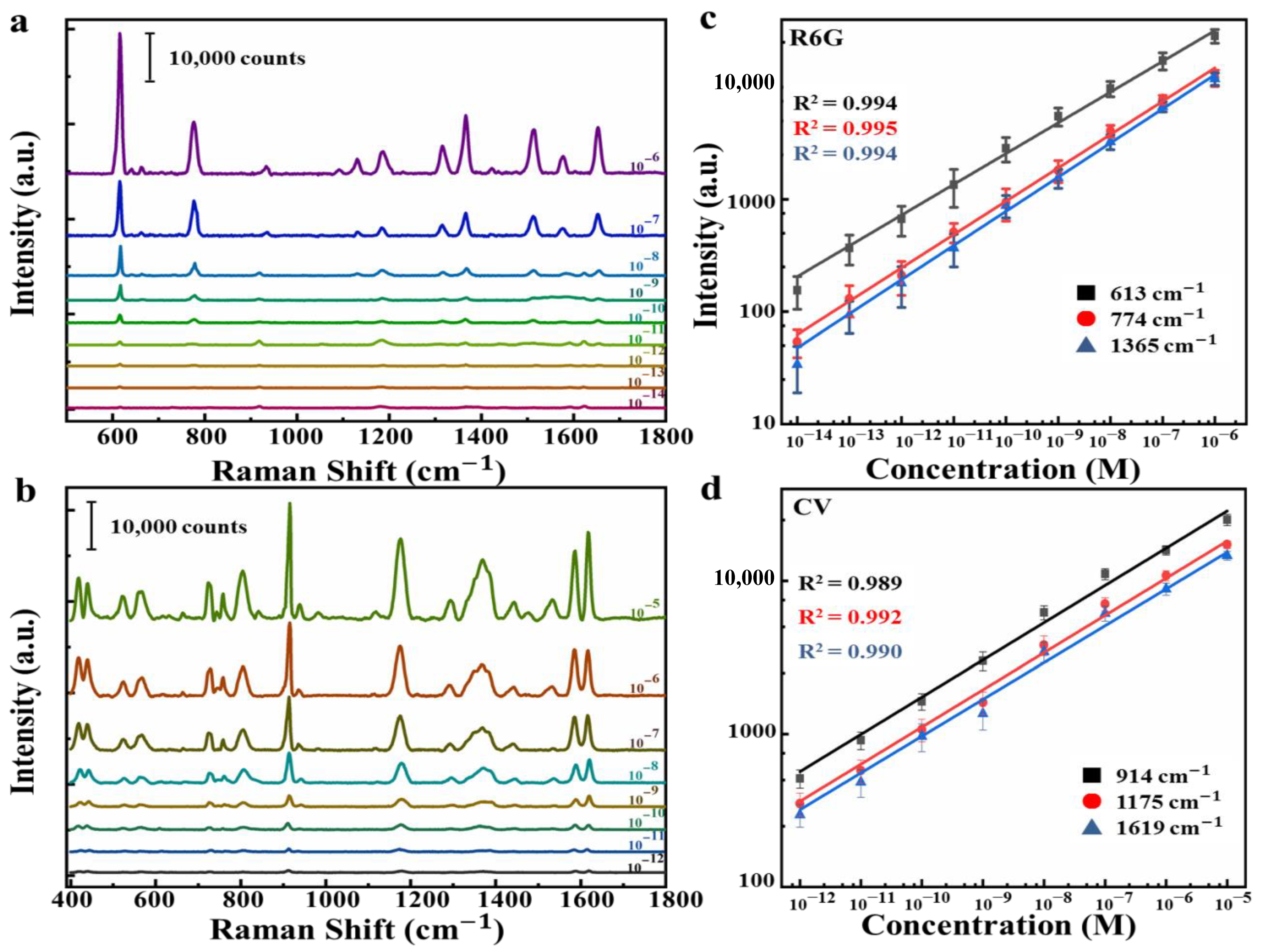
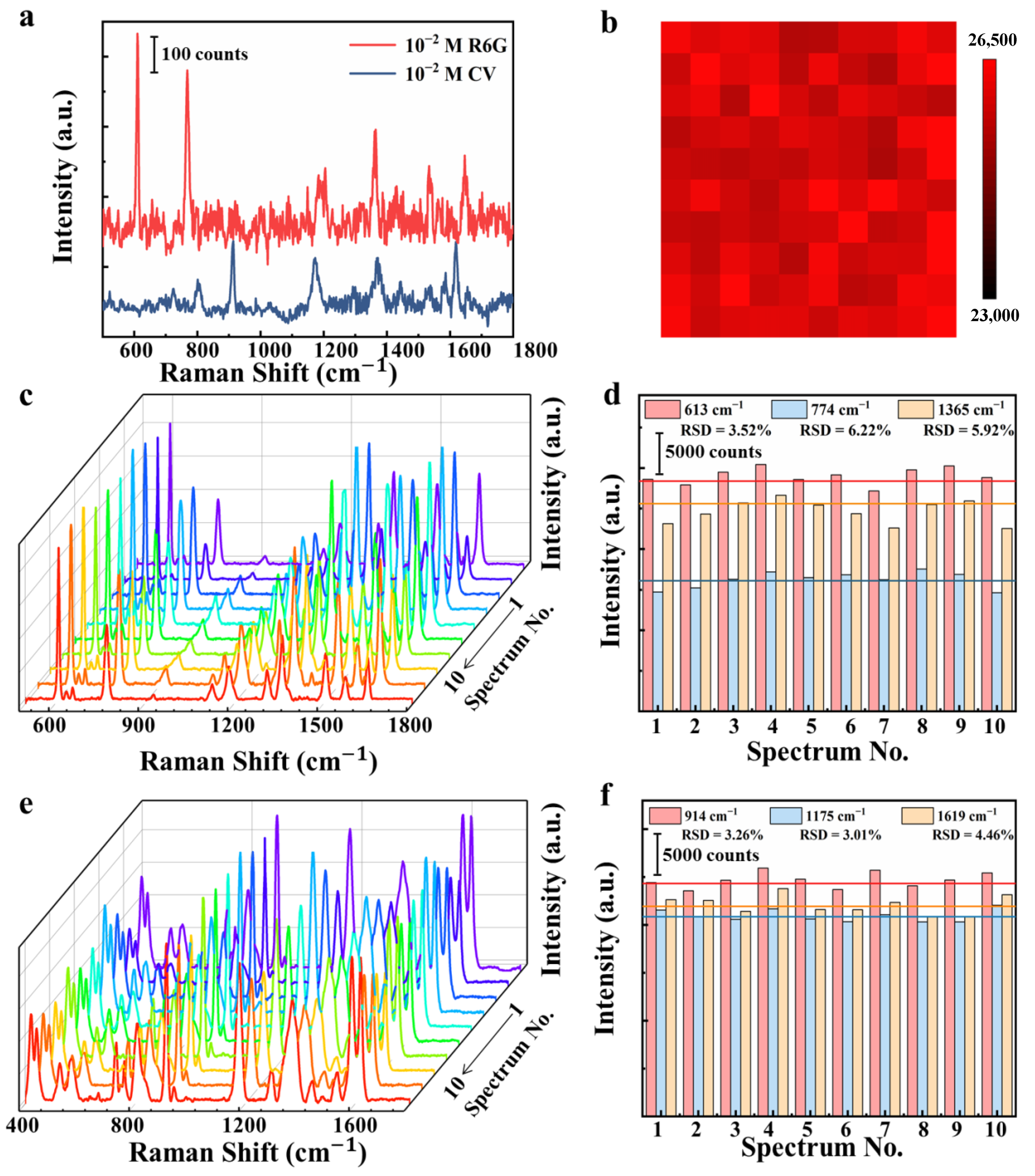
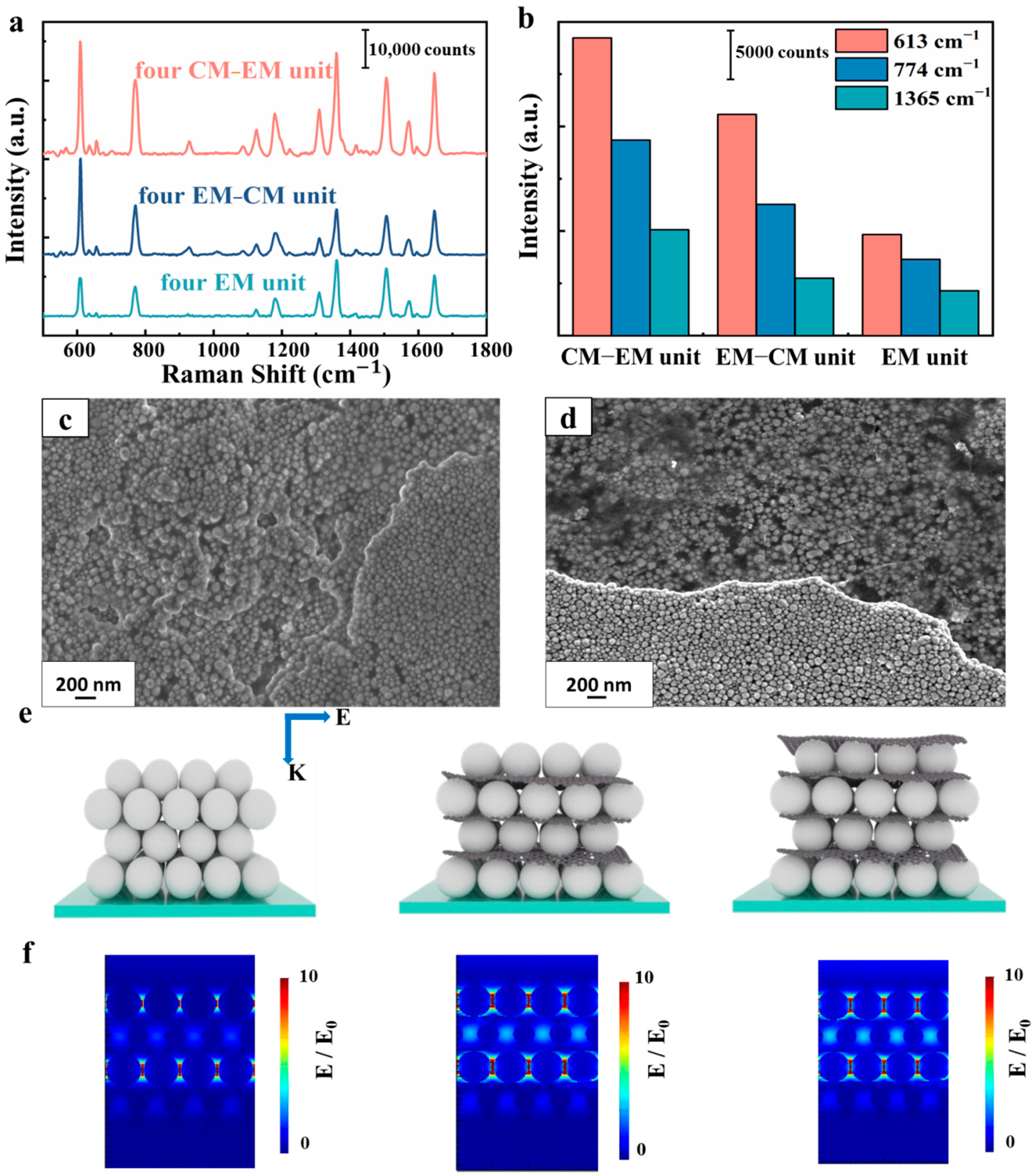
3. Results and Discussion
4. Conclusions
Supplementary Materials
Author Contributions
Funding
Conflicts of Interest
References
- Li, P.; Pan, D.; Yang, L.; Wei, H.; He, S.; Xu, H.; Li, Z. Silver nano-needles: Focused optical field induced solution synthesis and application in remote-excitation nanofocusing SERS. Nanoscale 2019, 11, 2153–2161. [Google Scholar] [CrossRef] [PubMed]
- Mu, X.; Sun, M. Interfacial charge transfer exciton enhanced by plasmon in 2D in-plane lateral and van der Waals heterostructures. Appl. Phys. Lett. 2020, 117, 091601. [Google Scholar] [CrossRef]
- Li, Z.; Jiang, S.; Huo, Y.; Ning, T.; Liu, A.; Zhang, C.; He, Y.; Wang, M.; Li, C.; Man, B. 3D silver nanoparticles with multilayer graphene oxide as a spacer for surface enhanced Raman spectroscopy analysis. Nanoscale 2018, 10, 5897–5905. [Google Scholar] [CrossRef]
- Ding, Q.; Wang, J.; Chen, X.; Liu, H.; Li, Q.; Wang, Y.; Yang, S. Quantitative and Sensitive SERS Platform with Analyte Enrichment and Filtration Function. Nano Lett. 2020, 20, 7304–7312. [Google Scholar] [CrossRef]
- Zhao, X.; Yu, J.; Zhang, Z.; Li, C.; Li, Z.; Jiang, S.; Pan, J.; Liu, A.; Zhang, C.; Man, B. Heterogeneous and cross-distributed metal structure hybridized with MoS2 as high-performance flexible SERS substrate. Opt. Express 2018, 26, 23831–23843. [Google Scholar] [CrossRef] [PubMed]
- Su, Y.; Zhang, Q.; Miao, X.; Wen, S.; Yu, S.; Chu, Y.; Lu, X.; Jiang, L.-P.; Zhu, J.-J. Spatially Engineered Janus Hybrid Nanozyme toward SERS Liquid Biopsy at Nano/Microscales. ACS Appl. Mater. Interfaces 2019, 11, 41979–41987. [Google Scholar] [CrossRef]
- Xu, K.; Zhou, R.; Takei, K.; Hong, M. Toward Flexible Surface-Enhanced Raman Scattering (SERS) Sensors for Point-of-Care Diagnostics. Adv. Sci. 2019, 6, 1900925. [Google Scholar] [CrossRef]
- Li, C.; Xu, S.; Yu, J.; Li, Z.; Li, W.; Wang, J.; Liu, A.; Man, B.; Yang, S.; Zhang, C. Local hot charge density regulation: Vibration-free pyroelectric nanogenerator for effectively enhancing catalysis and in-situ surface enhanced Raman scattering monitoring. Nano Energy 2020, 81, 105585. [Google Scholar] [CrossRef]
- Yu, J.; Guo, Y.; Wang, H.; Su, S.; Zhang, C.; Man, B.; Lei, F. Quasi Optical Cavity of Hierarchical ZnO Nanosheets@Ag Nanoravines with Synergy of Near- and Far-Field Effects for in Situ Raman Detection. J. Phys. Chem. Lett. 2019, 10, 3676–3680. [Google Scholar] [CrossRef]
- Yu, J.; Yang, M.; Li, Z.; Liu, C.; Wei, Y.; Zhang, C.; Man, B.; Lei, F. Hierarchical Particle-In-Quasicavity Architecture for Ultratrace In Situ Raman Sensing and Its Application in Real-Time Monitoring of Toxic Pollutants. Anal. Chem. 2020, 92, 14754–14761. [Google Scholar] [CrossRef]
- Xu, J.; Li, C.; Si, H.; Zhao, X.; Wang, L.; Jiang, S.; Wei, D.; Yu, J.; Xiu, X.; Zhang, C. 3D SERS substrate based on Au-Ag bi-metal nanoparticles/MoS2 hybrid with pyramid structure. Opt. Express 2018, 26, 21546–21557. [Google Scholar] [CrossRef]
- Zhao, X.; Liu, C.; Yu, J.; Li, Z.; Liu, L.; Li, C.; Xu, S.; Li, W.; Man, B.; Zhang, C. Hydrophobic multiscale cavities for high-performance and self-cleaning surface-enhanced Raman spectroscopy (SERS) sensing. Nanophotonics 2020, 9, 4761–4773. [Google Scholar] [CrossRef]
- Liu, Y.; Tian, X.; Guo, W.; Wang, W.; Guan, Z.; Xu, H. Real-time Raman detection by the cavity mode enhanced Raman scattering. Nano Res. 2019, 12, 1643–1649. [Google Scholar] [CrossRef]
- Dong, S.; Wang, Y.; Liu, Z.; Zhang, W.; Yi, K.; Zhang, X.; Zhang, X.; Jiang, C.; Yang, S.; Wang, F.; et al. Beehive-Inspired Macroporous SERS Probe for Cancer Detection through Capturing and Analyzing Exosomes in Plasma. ACS Appl. Mater. Interfaces 2020, 12, 5136–5146. [Google Scholar] [CrossRef] [PubMed]
- Ding, S.-Y.; Yi, J.; Li, J.-F.; Ren, B.; Wu, D.-Y.; Panneerselvam, R.; Tian, Z.-Q. Nanostructure-based plasmon-enhanced Raman spectroscopy for surface analysis of materials. Nat. Rev. Mater. 2016, 1, 16021. [Google Scholar] [CrossRef]
- Zhang, C.; Li, C.; Yu, J.; Jiang, S.; Xu, S.; Yang, C.; Liu, Y.J.; Gao, X.; Liu, A.; Man, B. SERS activated platform with three-dimensional hot spots and tunable nanometer gap. Sens. Actuators B Chem. 2018, 258, 163–171. [Google Scholar] [CrossRef]
- Zhang, C.; Jiang, S.Z.; Huo, Y.Y.; Liu, A.H.; Xu, S.C.; Liu, X.Y.; Sun, Z.C.; Xu, Y.Y.; Li, Z.; Man, B.Y. SERS detection of R6G based on a novel graphene oxide/silver nanoparticles/silicon pyramid arrays structure. Opt. Express 2015, 23, 24811–24821. [Google Scholar] [CrossRef]
- Ling, X.; Xie, L.; Fang, Y.; Xu, H.; Zhang, H.; Kong, J.; Dresselhaus, M.S.; Zhang, J.; Liu, Z. Can Graphene be used as a Substrate for Raman Enhancement? Nano Lett. 2010, 10, 553–561. [Google Scholar] [CrossRef]
- Xu, S.C.; Man, B.Y.; Jiang, S.Z.; Chen, C.S.; Yang, C.; Liu, M.; Gao, X.G.; Sun, Z.C.; Zhang, C. Flexible and transparent graphene-based loudspeakers. Appl. Phys. Lett. 2013, 102, 151902. [Google Scholar] [CrossRef]
- Li, Y.; Dykes, J.; Gilliam, T.; Chopra, N. A new heterostructured SERS substrate: Free-standing silicon nanowires decorated with graphene-encapsulated gold nanoparticles. Nanoscale 2017, 9, 5263–5272. [Google Scholar] [CrossRef] [Green Version]
- Marin, B.C.; Liu, J.; Aklile, E.; Urbina, A.D.; Chiang, A.S.C.; Lawrence, N.; Chen, S.; Lipomi, D.J. SERS-enhanced piezoplasmonic graphene composite for biological and structural strain mapping. Nanoscale 2017, 9, 1292–1298. [Google Scholar] [CrossRef] [PubMed] [Green Version]
- Liu, Y.; Luo, F. Spatial Raman mapping investigation of SERS performance related to localized surface plasmons. Nano Res. 2020, 13, 138–144. [Google Scholar] [CrossRef]
- Cao, E.; Lin, W.; Sun, M.; Liang, W.; Song, Y. Exciton-plasmon coupling interactions: From principle to applications. Nanophotonics 2018, 7, 145. [Google Scholar] [CrossRef]
- Tzeng, Y.; Chen, Y.; Lai, J.; Huang, B. Silver Nanoparticles SERS Sensors Using Rapid Thermal CVD Nanoscale Graphene Islands as Templates. IEEE Trans. Nanotechnol. 2020, 19, 25–33. [Google Scholar] [CrossRef]
- Anderson, W.J.; Nowinska, K.; Hutter, T.; Mahajan, S.; Fischlechner, M. Tuning plasmons layer-by-layer for quantitative colloidal sensing with surface-enhanced Raman spectroscopy. Nanoscale 2018, 10, 7138–7146. [Google Scholar] [CrossRef] [Green Version]
- Zhang, Y.-J.; Chen, S.; Radjenovic, P.; Bodappa, N.; Zhang, H.; Yang, Z.-L.; Tian, Z.-Q.; Li, J.-F. Probing the Location of 3D Hot Spots in Gold Nanoparticle Films Using Surface-Enhanced Raman Spectroscopy. Anal. Chem. 2019, 91, 5316–5322. [Google Scholar] [CrossRef]
- Kuttner, C. Plasmonics in Sensing: From Colorimetry to SERS Analytics; IntechOpen: London, UK, 2018. [Google Scholar]
- Guo, Y.; Yu, J.; Li, C.; Li, Z.; Pan, J.; Liu, A.; Man, B.; Wu, T.; Xiu, X.; Zhang, C. SERS substrate based on the flexible hybrid of polydimethylsiloxane and silver colloid decorated with silver nanoparticles. Opt. Express 2018, 26, 21784–21796. [Google Scholar] [CrossRef]
- Zhang, C.; Man, B.Y.; Yang, C.; Jiang, S.Z.; Liu, M.; Chen, C.S.; Xu, S.C.; Sun, Z.C.; Gao, X.G.; Chen, X.J. Facile synthesis of graphene on dielectric surfaces using a two-temperature reactor CVD system. Nanotechnology 2013, 24, 395603. [Google Scholar] [CrossRef]
- Zhao, X.; Li, C.; Li, Z.; Yu, J.; Pan, J.; Si, H.; Yang, C.; Jiang, S.; Zhang, C.; Man, B. In-situ electrospun aligned and maize-like AgNPs/PVA@Ag nanofibers for surface-enhanced Raman scattering on arbitrary surface. Nanophotonics 2019, 8, 1719. [Google Scholar] [CrossRef]
- Vial, A.; Laroche, T. Description of dispersion properties of metals by means of the critical points model and application to the study of resonant structures using the FDTD method. J. Phys. D 2007, 40, 7152–7158. [Google Scholar] [CrossRef]
- Yu, J.; Wei, Y.; Wang, H.; Zhang, C.; Wei, Y.; Wang, M.; Man, B.; Lei, F. In situ detection of trace pollutants: A cost-effective SERS substrate of blackberry-like silver/graphene oxide nanoparticle cluster based on quick self-assembly technology. Opt. Express 2019, 27, 9879–9894. [Google Scholar] [CrossRef] [PubMed]
- Malard, L.M.; Pimenta, M.A.; Dresselhaus, G.; Dresselhaus, M.S. Raman spectroscopy in graphene. Phys. Rep. 2009, 473, 51–87. [Google Scholar] [CrossRef]
- Ferrari, A.C.; Basko, D.M. Raman spectroscopy as a versatile tool for studying the properties of graphene. Nat. Nanotechnol. 2013, 8, 235–246. [Google Scholar] [CrossRef] [PubMed] [Green Version]
- Meng, X.; Wang, H.; Chen, N.; Ding, P.; Shi, H.; Zhai, X.; Su, Y.; He, Y. A Graphene–Silver Nanoparticle–Silicon Sandwich SERS Chip for Quantitative Detection of Molecules and Capture, Discrimination, and Inactivation of Bacteria. Anal. Chem. 2018, 90, 5646–5653. [Google Scholar] [CrossRef] [PubMed]
- Sun, H.; Yao, M.; Song, Y.; Zhu, L.; Dong, J.; Liu, R.; Li, P.; Zhao, B.; Liu, B. Pressure-induced SERS enhancement in a MoS2/Au/R6G system by a two-step charge transfer process. Nanoscale 2019, 11, 21493–21501. [Google Scholar] [CrossRef]
- Jeong, J.W.; Arnob, M.M.P.; Baek, K.-M.; Lee, S.Y.; Shih, W.-C.; Jung, Y.S. 3D Cross-Point Plasmonic Nanoarchitectures Containing Dense and Regular Hot Spots for Surface-Enhanced Raman Spectroscopy Analysis. Adv. Mater. 2016, 28, 8695–8704. [Google Scholar] [CrossRef] [PubMed]
- Wang, S.-Y.; Jiang, X.-X.; Xu, T.-T.; Wei, X.-P.; Lee, S.-T.; He, Y. Reactive ion etching-assisted surface-enhanced Raman scattering measurements on the single nanoparticle level. Appl. Phys. Lett. 2014, 104, 243104. [Google Scholar] [CrossRef]
- Zhang, Y.; Liu, S.; Wang, L.; Qin, X.; Tian, J.; Lu, W.; Chang, G.; Sun, X. One-pot green synthesis of Ag nanoparticles-graphene nanocomposites and their applications in SERS, H2O2, and glucose sensing. RSC Adv. 2012, 2, 538–545. [Google Scholar] [CrossRef]
- Gong, T.; Zhu, Y.; Zhang, J.; Ren, W.; Quan, J.; Wang, N. Study on surface-enhanced Raman scattering substrates structured with hybrid Ag nanoparticles and few-layer graphene. Carbon 2015, 87, 385–394. [Google Scholar] [CrossRef]
- Wang, X.; Wang, N.; Gong, T.; Zhu, Y.; Zhang, J. Preparation of graphene-Ag nanoparticles hybrids and their SERS activities. Appl. Surf. Sci. 2016, 387, 707–719. [Google Scholar] [CrossRef]
- Wu, J.; Xu, Y.; Xu, P.; Pan, Z.; Chen, S.; Shen, Q.; Zhan, L.; Zhang, Y.; Ni, W. Surface-enhanced Raman scattering from AgNP–graphene–AgNP sandwiched nanostructures. Nanoscale 2015, 7, 17529–17537. [Google Scholar] [CrossRef] [PubMed]
- Zhou, Y.; Cheng, X.; Du, D.; Yang, J.; Zhao, N.; Ma, S.; Zhong, T.; Lin, Y. Graphene–silver nanohybrids for ultrasensitive surface enhanced Raman spectroscopy: Size dependence of silver nanoparticles. J. Mater. Chem. C 2014, 2, 6850–6858. [Google Scholar] [CrossRef]
- Quan, J.; Zhang, J.; Li, J.; Zhang, X.; Wang, M.; Wang, N.; Zhu, Y. Three-dimensional AgNPs-graphene-AgNPs sandwiched hybrid nanostructures with sub-nanometer gaps for ultrasensitive surface-enhanced Raman spectroscopy. Carbon 2019, 147, 105–111. [Google Scholar] [CrossRef]


Publisher’s Note: MDPI stays neutral with regard to jurisdictional claims in published maps and institutional affiliations. |
© 2020 by the authors. Licensee MDPI, Basel, Switzerland. This article is an open access article distributed under the terms and conditions of the Creative Commons Attribution (CC BY) license (http://creativecommons.org/licenses/by/4.0/).
Share and Cite
Liu, L.; Hou, S.; Zhao, X.; Liu, C.; Li, Z.; Li, C.; Xu, S.; Wang, G.; Yu, J.; Zhang, C.; et al. Role of Graphene in Constructing Multilayer Plasmonic SERS Substrate with Graphene/AgNPs as Chemical Mechanism—Electromagnetic Mechanism Unit. Nanomaterials 2020, 10, 2371. https://0-doi-org.brum.beds.ac.uk/10.3390/nano10122371
Liu L, Hou S, Zhao X, Liu C, Li Z, Li C, Xu S, Wang G, Yu J, Zhang C, et al. Role of Graphene in Constructing Multilayer Plasmonic SERS Substrate with Graphene/AgNPs as Chemical Mechanism—Electromagnetic Mechanism Unit. Nanomaterials. 2020; 10(12):2371. https://0-doi-org.brum.beds.ac.uk/10.3390/nano10122371
Chicago/Turabian StyleLiu, Lu, Shuting Hou, Xiaofei Zhao, Chundong Liu, Zhen Li, Chonghui Li, Shicai Xu, Guilin Wang, Jing Yu, Chao Zhang, and et al. 2020. "Role of Graphene in Constructing Multilayer Plasmonic SERS Substrate with Graphene/AgNPs as Chemical Mechanism—Electromagnetic Mechanism Unit" Nanomaterials 10, no. 12: 2371. https://0-doi-org.brum.beds.ac.uk/10.3390/nano10122371