One-Way Zero Reflection in an Insulator-Metal-Insulator Structure Using the Transfer Matrix Method


1
Department of Physics, Kookmin University, Seoul 02707, Korea
2
Division of Science Education, Jeonbuk National University, Jeonju 54896, Korea
*
Author to whom correspondence should be addressed.
Photonics 2021, 8(1), 8; https://0-doi-org.brum.beds.ac.uk/10.3390/photonics8010008
Submission received: 11 December 2020
/
Revised: 25 December 2020
/
Accepted: 29 December 2020
/
Published: 31 December 2020
(This article belongs to the Special Issue Recent Advances in the Study of Light Propagation in Optical Fibers)
Abstract
:We numerically demonstrate one-way zero reflection using the transfer matrix method. Using simulations, we adjusted the thickness of SiO layers in a simple SiO-Au-SiO layer structure. We found two solutions, 47 nm-10 nm-32 nm and 71 nm-10 nm-60 nm, which are the thicknesses for one-way zero reflection at a wavelength of 560 nm. We confirmed it with reflection spectra, where reflectance is zero for forwardly incident light and 2.5% for backwardly incident light at the wavelength 560 nm, and thickness 47 nm-10 nm-32 nm.
1. Introduction
Many physical systems have a Hamiltonian with Hermitian properties, these properties lead to real and orthogonal eigenvalues. Recently Hamiltonians with parity-time (PT) symmetry have attracted a lot of interest because their eigenvalues are real below a certain threshold but are complex above that threshold [1]. PT-symmetric systems have a potential . Such a system can also be realized in optics [2,3]. If the permittivity, , of the system has symmetry such that , then PT-symmetry can be realized in an optical systems. Therefore, in order to satisfy PT-symmetry in optics, one should consider optical gain and loss in the system which, in turn, means should be represented as a complex number. This has been demonstrated many times in previous research [4,5,6,7].
One of the interesting phenomena in systems with PT-symmetry is the existence of an exceptional point. Exceptional point exists at the threshold where an eigenvalue changes from a real number to a complex number or vice versa. This behavior seems to be similar to that seen with degenerate states. The eigen modes, however, coalesce at an exceptional point. In other words, only one eigen mode can exist, which opens up the possibility of one-way reflection. There has been lots of research that has used this exceptional point in a variety of applications such as in single mode lasers or unidirectional reflectionlessness among others [8,9,10,11,12,13]. Recent progress in developing exceptional point-based research is well introduced in Ref. [14,15] and references therein.
Even though many physical systems use Hamiltonians to describe the physics at play, this is not the only way to describe PT-symmetry. Any kind of system can be considered, all that is required is that the PT-symmetry condition is satisfied. In optics, a scattering matrix (s-matrix) is often used to describe optical phenomena. Therefore, an s-matrix is also a candidate to describe PT-symmetric systems. One-way zero reflection has been obtained using an s-matrix in previous research [16,17,18]. Even though the theory for zero reflection comes from the use of an s-matrix, the reflection coefficient can be calculated with other methods. For layered structures, it is convenient to use the transfer matrix method (TMM) [19].
In this report, we use a three-layered structure that is composed of a metal layer sandwiched between two dielectric layers to obtain one-way zero reflection. We selected Au as a metal layer and SiO as dielectric layers which are favored materials in photonics research. Although there are demonstrations using Si-based structure [16,17], one-way zero reflection using the metal-based layer structure may also find its applications in various fields. By adjusting the thickness of the SiO layers, we obtain zero reflection for forwardly incident light while we get a nonzero reflection value for backwardly incident light.
2. Simulation
Reflection and transmission were obtained using TMM for the layered structure. The electric field relation between the mth layer and the th layer in the TMM is as follows.
where () is the electric field of forwardly (backwardly) propagating light; and are the refractive index and thickness of the mth layer, respectly; k is the wave number in a vacuum; and are the reflection and transmission coefficients when light propagates from the mth layer to the th layer. For normal incidence, the equations for and follow when relative permittivity is 1.
where is the refractive index of the th layer.
If the total number of layers is N and the electric field amplitude of incident light is 1, when the propagation direction of incident light is forward, we can write a matrix form of TMM as follows,
where , are the total reflection and transmission coefficients when the propagation direction of incident light is forward. When the propagation direction of incident light is backward, the relation is as follows,
In two port system, s-matrix can be expressed as . Because PT-symmetric system maintains reciprocity, . Furthermore, corresponding eignevalues are . When either or is zero, two eigenvalues coalesce to form exceptional points, i.e., the system has one-way zero reflection.
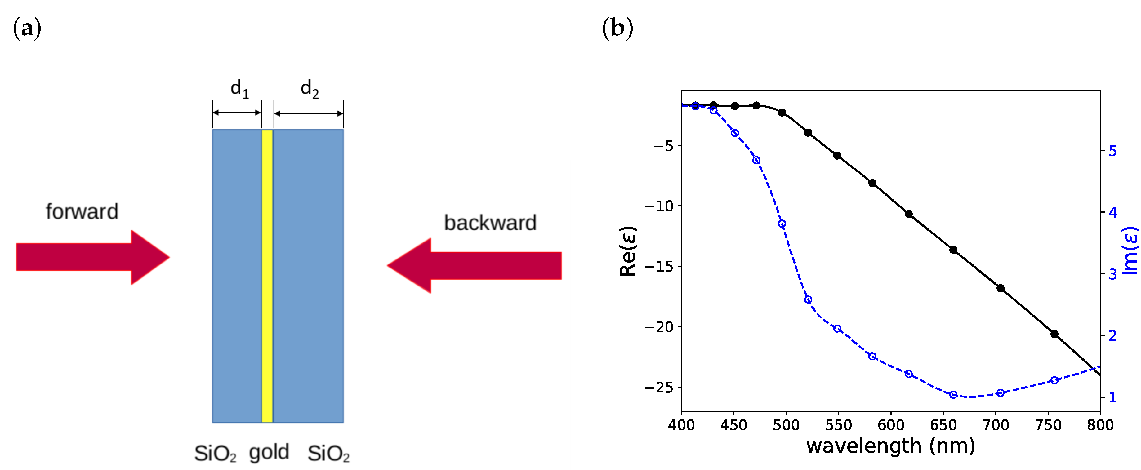
The structure for one-way zero reflection is depicted in Figure 1a. The structure presented consists of a SiO – Au – SiO layers in vacuum. The thickness of the gold is fixed at 10 nm. The reason for this is that Au is highly reflective in the visible wavelength range. If the thickness of Au is too high, we cannot achieve coupling between the light in the top SiO layer and that in the bottom SiO layer. On the other hand, if the thickness of the Au is too low, we will no longer be able to achieve a continuous film with the Au. The Au of 10 nm thickness is right above the percolation threshold [20]. The thicknesses of the top and bottom SiO layers are denoted by and , respectively. We adjusted and to achieve one-way zero reflection. The incident light from the left is denoted as forwardly incident light; the incident light from the right, backwardly incident light.
The relative permittivity, , is defined as . The of SiO is 2.13. As the permittivity of Au is strongly dispersive, its value changing with wavelength is not negligible so one fixed value cannot be used for a range of wavelengths. We used of Au from Ref. [21]. Figure 1b shows the dispersion of as a function of wavelength. Blue represents the real part of ; black represents the imaginary part of . The data points marked with the filled circles (•) and the open circles (∘) come from the reference, while the solid and dashed curves come from interpolation with the spline method. The real part of is negative because Au is a metal.
and are generally represented with complex numbers. Therefore, one can write and in terms of amplitude and phase. Using phase gives a great advantage when one is trying to find a zero for . As such, it is possible to find where by simply observing the phase of because there will be a phase change around the value zero [22]. We continuously adjusted and from 20 nm to 100 nm to find the phases of and .
Figure 2a,b show the false color images of the phases of and respectively, when the wavelength of the incident light is 560 nm. The colors indicate the phases of and . One can see that the phase changes by , i.e., the color changes from the darkest blue to the darkest red, if we move counterclockwise around the bottom-left point = (47 nm, 32 nm) of the dark line and around the top-right point = (71 nm, 60 nm) of the dark line, where the first and second numbers correspond to and , respectively. Therefore, we can see that becomes zero at and . , however, does not go to zero at and because there is no phase change around those points in false color image in Figure 2b. This indicates that one-way zero reflection has been realized at these points. It is also possible to get more accurate values for and by increasing the resolution of the false color image; this can be done by decreasing the scanning step, i.e., by reducing the interval we increment and while creating these false color image. Note that goes to zero at = (32 nm, 47 nm) and = (60 nm, 71 nm), where () is transposed of (). This is because the Au layer is embedded with the two SiO layers.
3. Results and Discussion
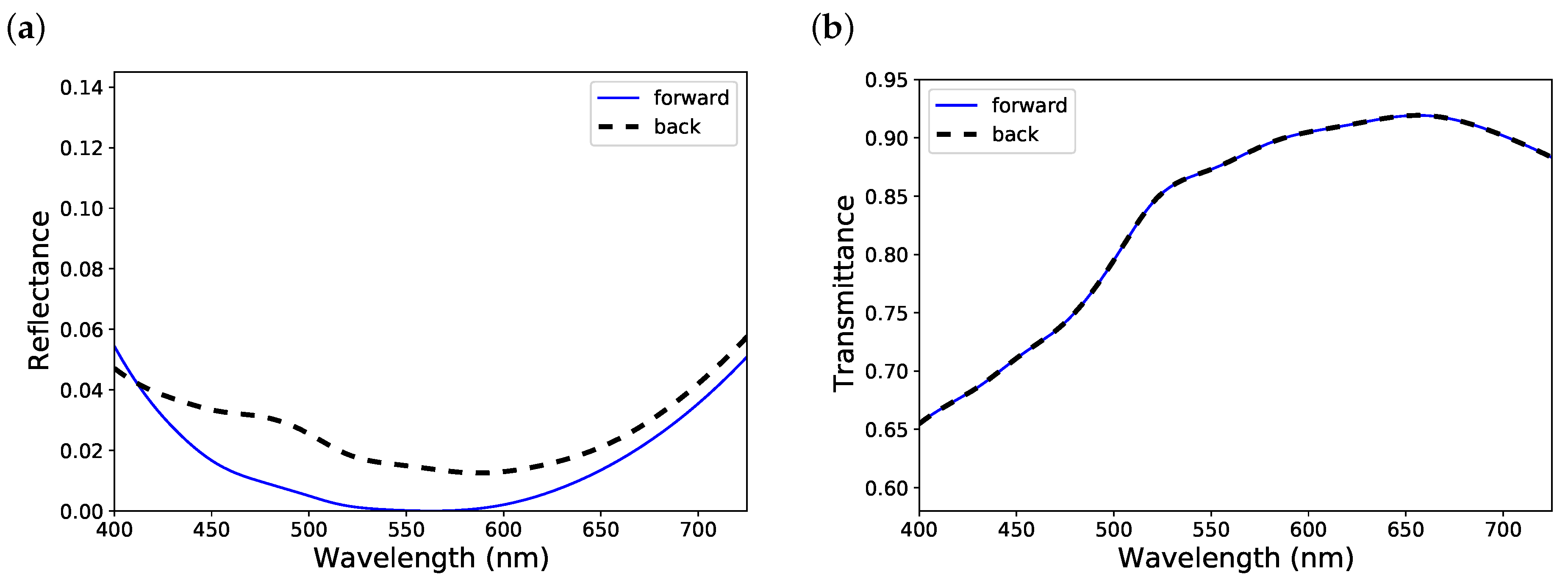
In order to confirm one-way zero reflection, we calculated the reflectance of the simulated structures: SiO(32 nm)-Au(10 nm)-SiO(47 nm) and SiO(60 nm)-Au(10 nm)-SiO(71 nm). Reflectance is defined as the square of the absolute value of the reflection coefficient. Therefore, with forwardly incident light the reflectance is , for backwardly incident light it is . Figure 3a shows the reflectance as a function of wavelength for nm and nm. The blue solid curve is for the reflectance of forwardly incident light, the black dashed curve is for the reflectance of backwardly incident light. The numerically calculated reflectance is less than for forwardly incident light while it is not zero but 2.5% for backwardly incident light at = 560 nm. These results confirm that we have one-way zero reflection at = 560 nm, which agrees with our simulation results presented in Figure 2. Figure 3b shows the transmittances of () for forwardly (backwardly) incident light. The blue solid curve shows the transmittance of forwardly incident light; the black dashed curve shows the transmittance of backwardly incident light. The blue solid and black dashed curves overlap exactly, which means the transmittance for forwardly incident light is the same as for backwardly incident light.
Figure 4a shows the reflectance as a function of wavelength for nm and nm. The blue solid curve shows the reflectance of forwardly incident light; the black dashed curve shows the reflectance of backwardly incident light. The numerically calculated reflectance is less that for forwardly incident light while it is not zero but 1.4% for backwardly incident light at 560 nm. These results confirm that we achieve one-way zero reflection at = 560 nm. Figure 4b shows the transmittance. The blue solid curve shows the transmittance of forwardly incident light, the black dashed curve shows the transmittance of backwardly incident light. The blue solid and black dashed curves overlaps exactly.
The reflectance and transmittance results indicate that the absorption is different for forwardly and backwardly incident light because . Figure 5 shows the absorption spectra of forwardly incident light (blue solid curve) and backwardly incident light (black dashed curve) as a function of wavelength for nm and nm (a), nm and nm (b). In both cases, absorption is higher for forwardly incident light compared to backwardly incident light.
4. Conclusions
We used TMM to simulate one-way zero reflection through an insulator-metal-insulator (IMI) structure. We used SiO for the two outer insulator layers and Au for the middle metal layer. By examining a range of thicknesses for both the SiO layers with the 10-nm Au layer at = 560 nm, we found two pairs of thicknesses that produced one-way zero reflection: 47 nm (60 nm) for the top layer and 32 nm (71 nm) for the bottom layer. We also confirmed one-way zero reflection using reflectance spectra. The reflectance becomes zero for forwardly incident light, while it is not zero for backwardly incident light. The reflectance of backwardly incident light is higher when nm and nm compared to when nm and nm.
Even though we used a metal as the absorption material, any material with absorption could be used to achieve one-way zero reflection, such as silicon demonstrated in prior research with various configurations [16,17]. IMI structure proposed in the context of one-way zero reflection may be adapted in optical fiber-based biosensors to investigate the possible increase of light coupling to the sensing region [23]. One-way zero reflection has great potential when applied in systems where no reflection is important, such as in solar cells.
Author Contributions
Conceptualization, H.N. and J.-M.C.; methodology, H.N.; investigation, H.N.; data curation, J.-M.C.; writing—original draft preparation, H.N.; writing—review and editing, J.-M.C.; visualization, J.-M.C.; supervision, H.N.; project administration, H.N.; funding acquisition, H.N. All authors have read and agreed to the published version of the manuscript.
Funding
This work was supported by the Basic Science Research Program through the National Research Foundation of Korea (NRF) funded by the Ministry of Education (No. 2017R1D1A1A02018515).
Institutional Review Board Statement
Not applicable.
Informed Consent Statement
Not applicable.
Conflicts of Interest
The authors declare no conflict of interest.
References
- Bender, C.M.; Boettcher, S. Real Spectra in Non-Hermitian Hamiltonians Having PT Symmetry. Phys. Rev. Lett. 1998, 80, 5243–5246. [Google Scholar] [CrossRef] [Green Version]
- Longhi, S.; Della Valle, G. Photonic Realization of PT-Symmetric Quantum Field Theories. Phys. Rev. A 2012, 85, 012112. [Google Scholar] [CrossRef]
- Bender, C.M. Making Sense of Non-Hermitian Hamiltonians. Rep. Prog. Phys. 2007, 70, 947–1018. [Google Scholar] [CrossRef] [Green Version]
- Musslimani, Z.H.; Makris, K.G.; El-Ganainy, R.; Christodoulides, D.N. Optical Solitons in PT Periodic Potentials. Phys. Rev. Lett. 2008, 100, 030402. [Google Scholar] [CrossRef] [PubMed]
- Guo, A.; Salamo, G.J.; Duchesne, D.; Morandotti, R.; Volatier-Ravat, M.; Aimez, V.; Siviloglou, G.A.; Christodoulides, D.N. Observation of PT-Symmetry Breaking in Complex Optical Potentials. Phys. Rev. Lett. 2009, 103, 093902. [Google Scholar] [CrossRef] [PubMed] [Green Version]
- Rüter, C.E.; Makris, K.G.; El-Ganainy, R.; Christodoulides, D.N.; Segev, M.; Kip, D. Observation of Parity-Time Symmetry in Optics. Nat. Phys. 2010, 6, 192–195. [Google Scholar] [CrossRef] [Green Version]
- Miri, M.-A.; LiKamWa, P.; Christodoulides, D.N. Large Area Single-Mode Parity–Time-Symmetric Laser Amplifiers. Opt. Lett. 2012, 37, 764. [Google Scholar] [CrossRef] [Green Version]
- Lin, Z.; Ramezani, H.; Eichelkraut, T.; Kottos, T.; Cao, H.; Christodoulides, D.N. Unidirectional Invisibility Induced by PT-Symmetric Periodic Structures. Phys. Rev. Lett. 2011, 106, 213901. [Google Scholar] [CrossRef] [Green Version]
- Liertzer, M.; Ge, L.; Cerjan, A.; Stone, A.D.; Türeci, H.E.; Rotter, S. Pump-Induced Exceptional Points in Lasers. Phys. Rev. Lett. 2012, 108, 173901. [Google Scholar] [CrossRef] [Green Version]
- Feng, L.; Xu, Y.L.; Fegadolli, W.S.; Lu, M.H.; Oliveira, J.E.B.; Almeida, V.R.; Chen, Y.F.; Scherer, A. Experimental Demonstration of a Unidirectional Reflectionless Parity-Time Metamaterial at Optical Frequencies. Nat. Mater. 2013, 12, 108–113. [Google Scholar] [CrossRef]
- Brandstetter, M.; Liertzer, M.; Deutsch, C.; Klang, P.; Schöberl, J.; Türeci, H.E.; Strasser, G.; Unterrainer, K.; Rotter, S. Reversing the Pump Dependence of a Laser at an Exceptional Point. Nat. Commun. 2014, 5, 4034. [Google Scholar] [CrossRef] [PubMed] [Green Version]
- Feng, L.; Wong, Z.J.; Ma, R.M.; Wang, Y.; Zhang, X. Single-Mode Laser by Parity-Time Symmetry Breaking. Science 2014, 346, 972–975. [Google Scholar] [CrossRef] [PubMed]
- Hodaei, H.; Miri, M.A.; Hassan, A.U.; Hayenga, W.E.; Heinrich, M.; Christodoulides, D.N.; Khajavikhan, M. Parity-Time-Symmetric Coupled Microring Lasers Operating around an Exceptional Point. Opt. Lett. 2015, 40, 4955. [Google Scholar] [CrossRef] [PubMed]
- Miri, M.-A.; Alú, A. Exceptional points in optics and photonics. Science 2019, 363, eaar7709. [Google Scholar] [CrossRef] [Green Version]
- Wiersig, J. Review of exceptional point-based sensors. Photonics Res. 2020, 8, 1457–1467. [Google Scholar] [CrossRef]
- Shen, Y.; Deng, X.H.; Chen, L. Unidirectional Invisibility in a Two-Layer Non-PT-Symmetric Slab. Opt. Express 2014, 22, 19440. [Google Scholar] [CrossRef]
- Feng, L.; Zhu, X.; Yang, S.; Zhu, H.; Zhang, P.; Yin, X.; Wang, Y.; Zhang, X. Demonstration of a Large-Scale Optical Exceptional Point Structure. Opt. Express 2014, 22, 1760. [Google Scholar] [CrossRef]
- Huang, Y.; Veronis, G.; Min, C. Unidirectional Reflectionless Propagation in Plasmonic Waveguide-Cavity Systems at Exceptional Points. Opt. Express 2015, 23, 29882. [Google Scholar] [CrossRef]
- Na, J.; Noh, H. Investigation of a Broadband Coherent Perfect Absorber in a Multi-Layer Structure by Using the Transfer Matrix Method. J. Korean Phys. Soc. 2018, 72, 66–70. [Google Scholar] [CrossRef]
- Ducourtieux, S.; Podolskiy, V.A.; Grésillon, S.; Buil, S.; Berini, B.; Gadenne, P.; Boccara, A.C.; Rivoal, J.C.; Bragg, W.D.; Banerjee, K.; et al. Near-Field Optical Studies of Semicontinuous Metal Films. Phys. Rev. B 2001, 64, 1654031–16540314. [Google Scholar] [CrossRef] [Green Version]
- Johnson, P.B.; Christy, R.W. Optical Constants of the Noble Metals. Phys. Rev. B 1972, 6, 4370–4379. [Google Scholar] [CrossRef]
- Andreasen, J.; Vanneste, C.; Ge, L.; Cao, H. Effects of Spatially Nonuniform Gain on Lasing Modes in Weakly Scattering Random Systems. Phys. Rev. A 2010, 81, 043818. [Google Scholar] [CrossRef] [Green Version]
- González-Vila, Á.; Debliquy, M.; Lahem, D.; Zhang, C.; Mégret, P.; Caucheteur, C. Molecularly imprinted electropolymerization on a metal-coated optical fiber for gas sensing application. Sens. Actuators B Chem. 2017, 244, 1145–1151. [Google Scholar] [CrossRef]
Figure 1.
(a) Schematic of simulated structure. The three layers seen here are SiO-Au-SiO. We fixed the thickness of Au as 10 nm, and and are varied to achieve one-way zero reflection. Incident light coming from the left (right) is denoted as forwardly (backwardly) incident light. (b) dispersion curve of Au. The data points marked with the black filled circles (•) and the blue open circles (∘) are from Ref. [21]. Solid and dashed curves are lines of best fit. The black curves represents the real part of , the blue curves represents the imaginary part of .

Figure 2.
The false color image showing the phases of (a) and (b). (a) at = (47 nm, 32 nm) and = (71 nm, 60 nm) because a phase change of occurs around these points. (b) at = (32 nm, 47 nm) and = (60 nm, 71 nm), where the first and second numbers correspond to and , respectively.
Figure 2.
The false color image showing the phases of (a) and (b). (a) at = (47 nm, 32 nm) and = (71 nm, 60 nm) because a phase change of occurs around these points. (b) at = (32 nm, 47 nm) and = (60 nm, 71 nm), where the first and second numbers correspond to and , respectively.

Figure 3.
Reflectance and transmittance for a structure with nm and nm (a) Reflectance of forwardly incident light (blue solid curve) and backwardly incident light (black dashed curve) as a function of wavelength. Only reflectance of forwardly incident light becomes zero at 560 nm. (b) Transmittance of forwardly incident light (blue solid curve) and backwardly incident light (black dashed curve) as a function of wavelength. The transmittance is the same for both forwardly and backwardly incident light.

Figure 4.
Reflectance and transmittance for a structure with nm and nm (a) Reflectance of forwardly incident light (blue solid curve) and backwardly incident light (black dashed curve) as a function of wavelength. Only the reflectance of forwardly incident light becomes zero at 560 nm. (b) Transmittance of forwardly incident light (blue solid curve) and backwardly incident light (black dashed curve) as a function of wavelength. The transmittance is the same for both forwardly and backwardly incident light.

Figure 5.
Absorption spectra of forwardly incident light (blue solid curve) and backwardly incident light (black dashed curve) as a function of wavelength for a structure with nm and nm (a), nm and nm (b).
Figure 5.
Absorption spectra of forwardly incident light (blue solid curve) and backwardly incident light (black dashed curve) as a function of wavelength for a structure with nm and nm (a), nm and nm (b).

Publisher’s Note: MDPI stays neutral with regard to jurisdictional claims in published maps and institutional affiliations. |
© 2020 by the authors. Licensee MDPI, Basel, Switzerland. This article is an open access article distributed under the terms and conditions of the Creative Commons Attribution (CC BY) license (http://creativecommons.org/licenses/by/4.0/).
Share and Cite
MDPI and ACS Style
Noh, H.; Choi, J.-M. One-Way Zero Reflection in an Insulator-Metal-Insulator Structure Using the Transfer Matrix Method. Photonics 2021, 8, 8. https://0-doi-org.brum.beds.ac.uk/10.3390/photonics8010008
AMA Style
Noh H, Choi J-M. One-Way Zero Reflection in an Insulator-Metal-Insulator Structure Using the Transfer Matrix Method. Photonics. 2021; 8(1):8. https://0-doi-org.brum.beds.ac.uk/10.3390/photonics8010008
Chicago/Turabian StyleNoh, Heeso, and Jai-Min Choi. 2021. "One-Way Zero Reflection in an Insulator-Metal-Insulator Structure Using the Transfer Matrix Method" Photonics 8, no. 1: 8. https://0-doi-org.brum.beds.ac.uk/10.3390/photonics8010008
Note that from the first issue of 2016, this journal uses article numbers instead of page numbers. See further details here.