All-Metal Terahertz Metamaterial Absorber and Refractive Index Sensing Performance


Institute of Optoelectronic Technology, China Jiliang University, Hangzhou 310018, China
*
Author to whom correspondence should be addressed.
Photonics 2021, 8(5), 164; https://0-doi-org.brum.beds.ac.uk/10.3390/photonics8050164
Submission received: 29 April 2021
/
Revised: 9 May 2021
/
Accepted: 11 May 2021
/
Published: 14 May 2021
(This article belongs to the Special Issue Advanced Metamaterials and Metadevices)
Abstract
:This paper presents a terahertz (THz) metamaterial absorber made of stainless steel. We found that the absorption rate of electromagnetic waves reached 99.95% at 1.563 THz. Later, we analyzed the effect of structural parameter changes on absorption. Finally, we explored the application of the absorber in refractive index sensing. We numerically demonstrated that when the refractive index (n) is changing from 1 to 1.05, our absorber can yield a sensitivity of 74.18 μm/refractive index unit (RIU), and the quality factor (Q-factor) of this sensor is 36.35. Compared with metal–dielectric–metal sandwiched structure, the absorber designed in this paper is made of stainless steel materials with no sandwiched structure, which greatly simplifies the manufacturing process and reduces costs.
1. Introduction
Metamaterials are new artificial materials that are periodically arranged according to certain subwavelength dimensions [1,2]. Owing to their unique properties of perfect absorption, perfect transmission, and stealth, metamaterials show promising applications in sensors [3,4,5,6,7,8,9,10,11], absorbers [12,13], imaging [14,15], etc. Among them, in biomolecular sensing, metamaterial devices are spurring unprecedented interest as a diagnostic protocol for cancer and infectious diseases [10,11]. Terahertz radiation [16] refers to the frequency range of 0.1 to 10 THz, between the microwave and infrared bands. Since natural materials rarely interact with terahertz frequencies, artificial metamaterials have opened up a new way to interact with terahertz waves. Terahertz technology has great potential in the fields of broadband communications, detection, chemistry, and medicine, among which terahertz sensing plays a huge role in material detection. Absorbers based on metamaterials are receiving increasing attention. In 2008, Landy et al. designed a “perfect” metamaterial absorber, which can achieve nearly 100% absorption in the microwave band [13]. Later in the same year, Hu Tao et al. [17] proposed an absorber with a metal ring resonator and a branch line separated by a dielectric. Based on Landy’s discovery, this absorber achieved nearly perfect absorption in the THz band for the first time and reached a micron-level structure. In 2009, Landy et al. designed an absorber with an improved electrically coupled ring resonator that achieved 95% absorption at 1.13 THz [18]. The proposed absorber has created new opportunities for investigating metamaterial absorbers [13,19,20]. These characteristics have led to a research boom in THz absorbers [17]. In the subsequent research, various perfect absorption schemes based on metamaterials have been proposed, whose working ranges are microwave, THz [17,18,21], infrared [22,23,24,25], and visible light wavelength band [26,27,28]. Nanocavities composed of different absorbing metamaterials exhibit extraordinary optical effects such as extraordinary absorption and zero reflection at resonant wavelengths, which opens a wide scenario of applications in fields such as tunable color filters, photonics, physical security, and sensing [28].
Recently, metamaterial absorbers have opened up a new sensing approach, which is widely used in medical testing, environmental testing, and food safety. In 2016, Yongzhi Cheng et al. designed a nonplanar all-metal plasmonic perfect absorber with a sensitivity of 1.445 μm/RIU in the infrared region [29]. In the same year, the metal–insulator–metal metamaterial absorber was proved to achieve a sensitivity of 0.43 μm/RIU [30]. In 2020, Yunping Qi et al. proposed a tunable terahertz metamaterial absorber composed of an elliptical ring graphene array with a sensitivity of 14.11 μm/RIU [31]. In the above, the structure is complex and the sensitivity is not high. Therefore, designing an absorber with high sensitivity is an urgent problem to be solved. Optical dispersion metasurfaces can be used for the detection of ultralow-molecular-weight molecules with extremely low concentrations on the whole surface array [10,11]. Terahertz radiation can achieve the local enhancement of electromagnetic field in the metasurface, thus achieving high sensitivity.
In this paper, a novel metamaterial absorber made of stainless steel is proposed. This absorber can achieve 99.95% absorption at 1.563 THz. We explored the absorption mechanism from the distribution of electric and magnetic fields. The resonant frequency and peak absorption can be varied by changing the structural parameters. Finally, the refractive index sensing of this absorber was explored. When the refractive index changes from 1 to 1.05, our absorber can achieve a sensitivity of 74.18 μm/RIU and a quality factor of 36.35.
2. Structural Design and Simulation
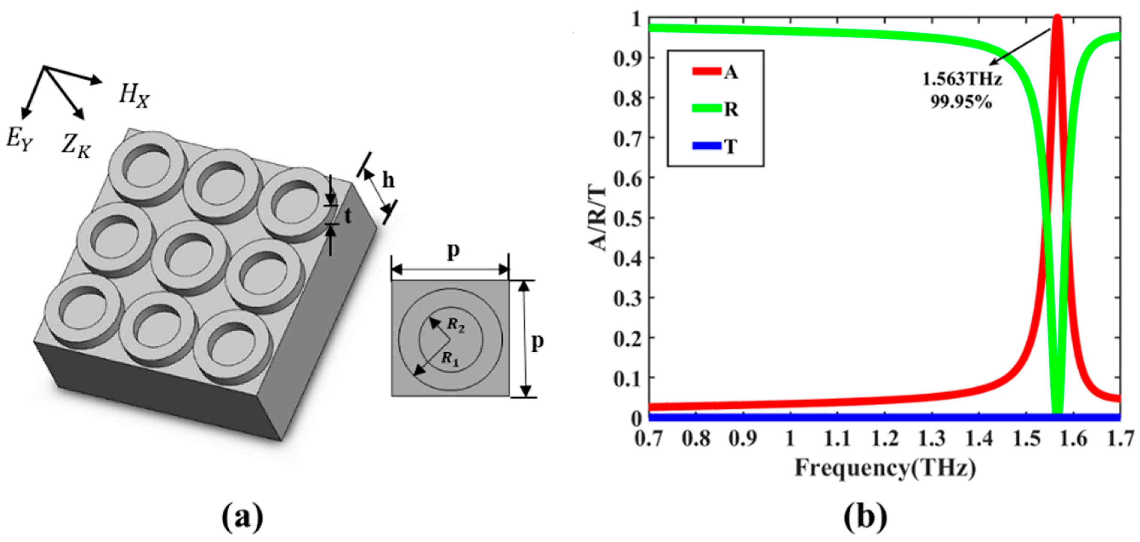
The stainless steel THz absorber schematic diagram is shown in Figure 1a. The structure is mainly composed of a metal metamaterial layer and a substrate layer. The shape of the metal metamaterial layer is a ring. The outer radius R1 and inner radius R2 of the ring are 80 µm and 60 µm, respectively. The thicknesses of the metal metamaterial layer and the substrate layer are respectively denoted by t and h, where t is 30 µm and h is 200 nm. The unit cell period p of the absorber is 170 µm. Both the metal metamaterial layer and the substrate layer are made of stainless steel with an electric conductivity of 1.4 × 10⁶ S/m. In this work, we chose stainless steel instead of the usual gold, silver, and aluminum, because stainless steel as an alloy metal has the advantages of corrosion resistance and high hardness. In addition, as a kind of material of 3D printing, stainless steel makes it possible to realize our absorber through simple manufacturing technology. The electromagnetic simulation software CST was used to calculate the numerical absorption using the frequency domain solver. In the simulation, the unit cell boundary condition was arranged in both x and y directions, and an open boundary condition was used in the wave propagation direction. The wave vector k of the incident electromagnetic wave was assumed to be a plane wave, propagating along the negative z-axis. We defined the electric field transverse along the x-axis as the TE mode and the magnetic field transverse along the x-axis as the TM mode. In our study, simulation results were obtained under TM mode as shown in Figure 1a. The absorption (A) can be calculated as A(w) = 1 − R(w) − T(w), where T and R are the transmittance and reflectivity of the absorber, respectively. The thickness of the continuous stainless steel substrate layer as the metallic ground plate used here is much larger than the typical skin depth approximately 150 nm in the terahertz band; therefore, no transmission could be examined. Consequently, the absorption can be written as A(w) = 1 − R (w).
Figure 1b is the reflection, transmission, and absorption spectrum of the structure from 0.7 to 1.7 THz. By observing the simulation results, we found that the structure achieved a narrow absorption peak at 1.563 THz, and the absorption rate reached 99.95%. Q-factor can be obtained from Q = f/FWHM [32], where FWHM is the full width at half maximum and f is the frequency of electromagnetic waves. The FWHM of the absorber is 0.043 THz, and the Q is 36.35.
We can use the impedance matching mechanism to explain the existence of absorption peaks of stainless steel absorbers. First, a theory with the effective medium theory (EMT) is proposed. The absorber structure designed in this paper is considered to be homogeneous. The S-parameter and impedance Z are expressed by the following equation [33,34]:
where S21 is the transmission coefficient, S11 is the reflection coefficient, n is the effective refractive index of the absorber, k is the wave vector, and l is the thickness of the absorber. After calculating the above formulas, the impedance Z and absorption A are obtained:
The free space impedance Z0 is equal to 1. When the impedance matches the free space impedance at the operating frequency (Z0 = Z = 1), a nearly perfect absorption can be obtained. The impedance of the absorption peak near 1.563 THz is calculated to be closer to 1.
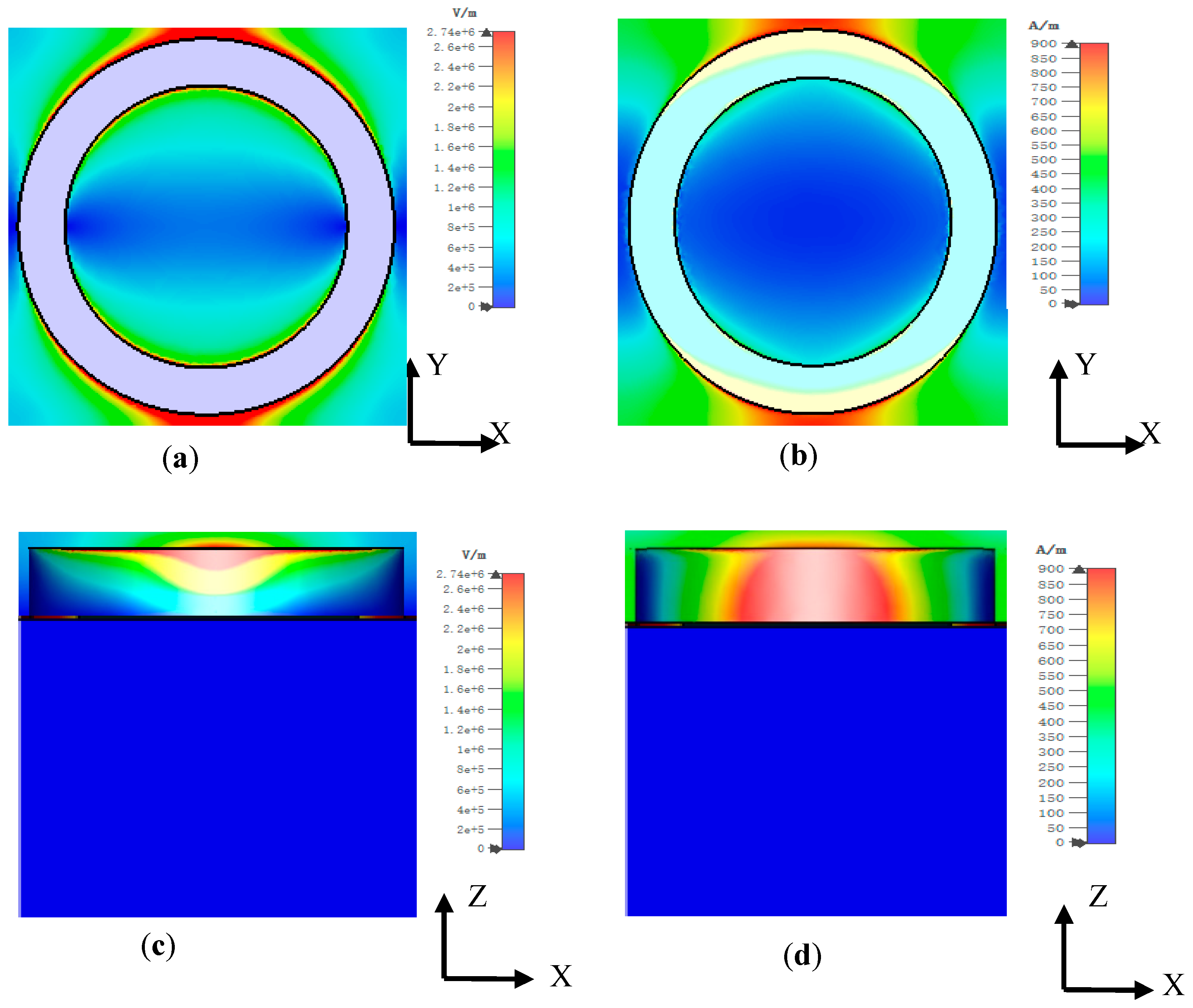
In order to explain the principle of the absorption peak generated by this absorber more vividly, we analyzed the electric and magnetic field distribution at the resonant frequency 1.563 THz. Figure 2a,b show the electric and magnetic field distribution of the stainless steel absorber on the upper surface of the ring and Figure 2c,d show the electric and magnetic field distribution of the stainless steel absorber at the ring x-z cross-section at 1.563 THz, respectively. As can be seen from Figure 2a,b, there is strong electric and magnetic field enhancement at the ring’s edge. Figure 2c,d show that the electric and magnetic field is focused primarily on the air slot of the ring metamaterial layer. The local enhancement of electric and magnetic fields indicates strong electrical and magnetic resonances [35,36]. The resonance mode can be obtained by the decomposition of dipole scattered powers [37]. Electric dipole P and magnetic dipole M mainly contribute to the resonant peak. In addition, the air slot of the ring increases the coupling of electromagnetic waves to achieve strong peak absorption. In summary, the combination of electrical and magnetic resonances produces a strong peak absorption at 1.563 THz.
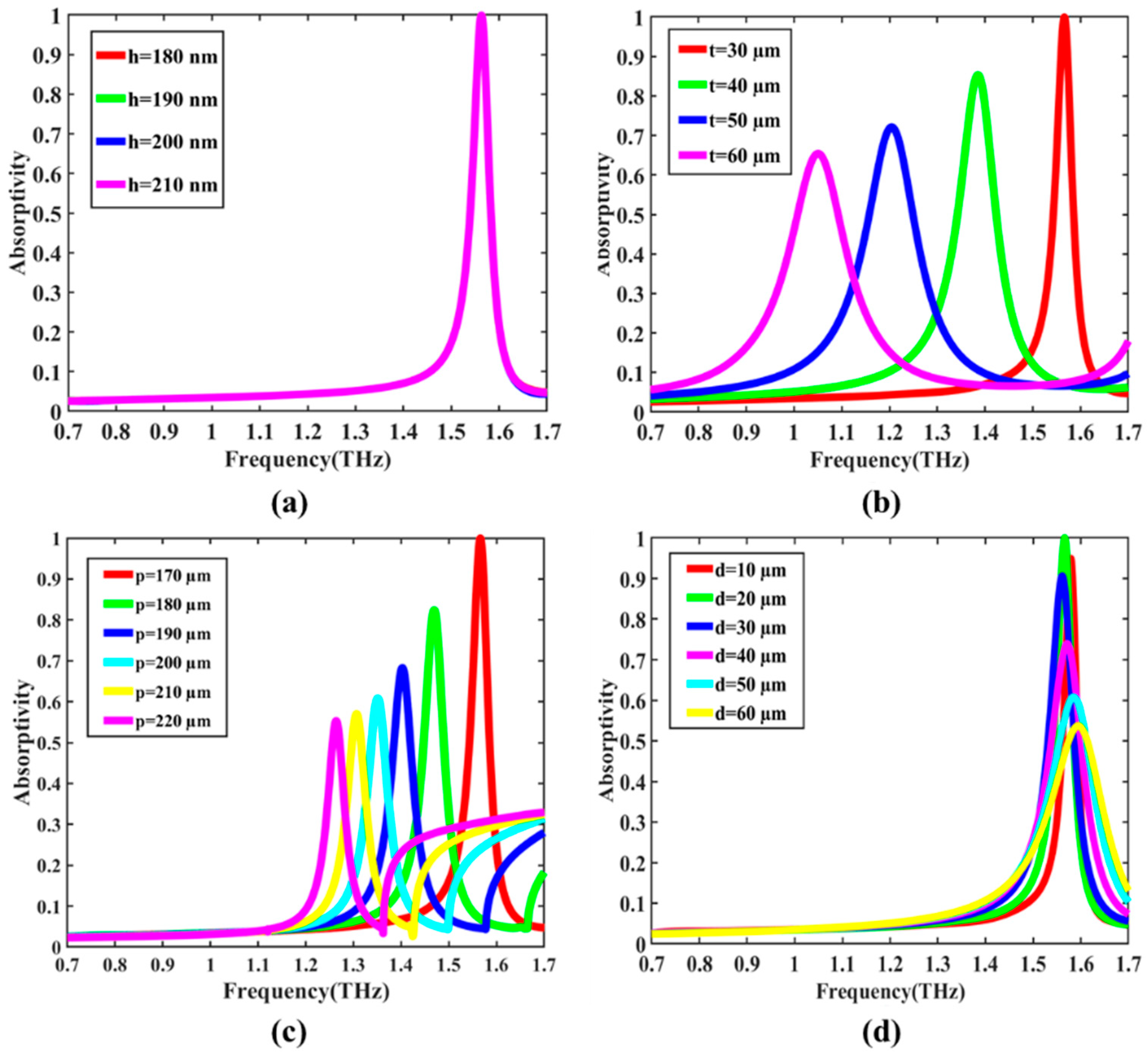
We also assessed the influence of geometry on absorption performance. First, we adjusted the thickness h of the substrate layer to observe the impact of the absorber’s absorption performance. The base thickness h was 180, 190, 200, and 210 nm, as shown in Figure 3a. Changing the thickness h of the base had no effect on the absorption performance. This is because the thickness of the continuous stainless steel substrate layer used here is much larger than the typical skin depth in the terahertz band; therefore, no transmission could be examined. We also found that the change of h does not affect the terahertz absorption. Next, we changed the thickness t of the metal metamaterial layer. The absorption curve when t is 30, 40, 50, and 60 µm is shown in Figure 3b. The absorption peak gradually moves to the left as t increases, and the peak absorption is reduced. This is because when t changes, the overall thickness of the absorber structure changes, breaking the frequency point and impedance value at the impedance match. We can design the thickness of the metal metamaterial layer according to actual needs to obtain a specific bandwidth absorption response.
Then, we plotted the absorption spectrum to assess the influence of the value of the period p. The absorption curve when p is 170, 180, 190, 200, 210, and 220 µm is shown in Figure 3c. When p increases, the absorption peak shifts significantly to the left, and the peak value decreases. This is because when period p increases, the volume occupied by the ring metamaterial layer decreases, causing the electrical and magnetic resonance to weaken. It is worth noting that when the absorption peak shifts to the left, there a lack of flatness after the absorption peak. In the case of p = 170 μm, the phenomenon of the lack of flatness after absorption peak also exists, which is not shown in the frequency band. The uneven effect is caused by the other resonance modes. Finally, we define d, which represents the difference between radii and of the ring of the metal metamaterial layer. In our simulation, outer radius R1 does not change, keeping the value of 80 μm; only the inner radius R2 is changed to realize the change of d. The absorption curve when d is 10, 20, 30, 40, 50, and 60 µm is shown in Figure 3d. When d increases, the absorption peak shifts first to the left and then to the right, and the peak increases first and then decreases. The change in the resonant peak is due to the variation in the space occupied by the air slot, which has an influence on the coupling of electromagnetic waves inside the structure. It is found that the absorption peak is the highest when d = 20 µm. In order to obtain high absorption in the THz region and make the absorber have narrower broadband for subsequent refractive index sensing, the optimized parameters of the stainless steel absorber presented in this paper were found to be p = 170 µm, t = 30 µm, h = 200 nm, d = 20 µm.
3. Refractive Index Sensing
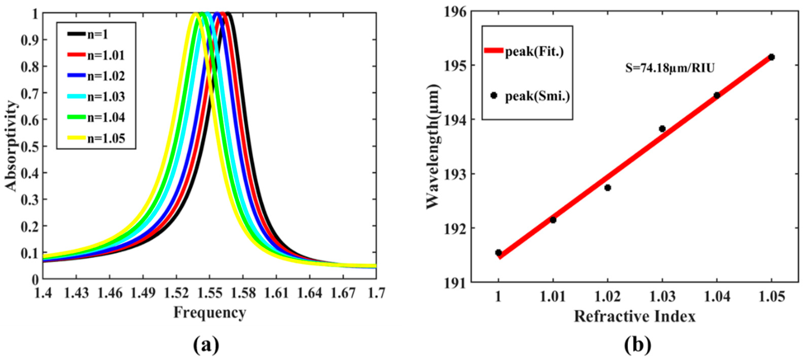
In order to further explore the potential value of the stainless steel absorber proposed in this paper, we analyzed the sensing performance of the absorber based on the narrow absorption characteristics. The hollow disk structure can not only increase the coupling of electromagnetic waves to achieve a high absorption effect but also increase the sensing area to achieve an obvious sensing effect. Figure 4a demonstrates the relationship between the absorption spectrum and different refractive indexes. In our simulation, we investigated the dependence of the absorption spectra on the refractive index with an overlayer thickness of 50 μm. When n increases from 1.0 to 1.05 with a step of 0.01, the resonant peak changes from 1.563 to 1.537 THz, corresponding to the wavelength range from 191.546 to 195.147 μm. It is worth noting that peak absorption is almost constant when the resonant frequency appears red-shifted. Sensitivity is a vital parameter to evaluate sensing performance. Sensitivity can be obtained from S = Δλ/Δn, where Δλ and Δn are the changes in the values of resonant wavelength and n [38,39]. Figure 4b illustrates the relationship between Δλ and Δn, where the slope of the line can be regarded as the sensitivity of the sensor. The S of our absorber reaches approximately 74.18 μm/RIU. In addition, the function between the resonance wavelength and n is also shown in Formula 5, expressed as follows:
y = 74.18x + 117.27
4. Conclusions
In this paper, a terahertz absorber made of stainless steel has been proposed, and its use for refractive index sensing has been described. This absorber consists of all-metal metamaterial layers and substrate layers, where the geometric shape of the metamaterial layer is a ring. The research proves the theoretical feasibility and superior sensing performance. Simulation results show that the absorber reaches a 99.95% narrow peak absorption at 1.563 THz. Specifically, the absorption can be tuned by geometric parameters. The electric and magnetic resonances of the ring metamaterial layer enabled this high absorption efficiency. The absorber shows a distinct difference in the resonant frequency for different refractive indexes, and the sensitivity of the sensor is 74.18 μm/RIU with the Q-factor of 36.35. Additionally, the absorber designed in this paper is made of stainless steel and has no sandwiched structure. The stainless steel material costs less and is easy to process, making it possible to apply in various fields. Our work can provide potential applications in optoelectronic devices, biosensors, and optical switching.
Author Contributions
J.Y. wrote the paper, T.L. conceived and designed simulation, H.C. completed editing and review. All authors have read and agreed to the published version of the manuscript.
Funding
This work was supported by the National Natural Science Foundation of China (61875251, 61875179), the Fundamental Research Funds for the Provincial Universities of Zhejiang (2020YW08), and the Outstanding Student Achievement Cultivation Program of China Jiliang University (2019YW27).
Institutional Review Board Statement
Not applicable.
Informed Consent Statement
Not applicable.
Data Availability Statement
Not applicable.
Conflicts of Interest
The authors declare no conflict of interest.
References
- Shalaev, V.M. Optical negative-index metamaterials. Nat. Photonics 2007, 1, 41–48. [Google Scholar] [CrossRef]
- Zheludev, N.I.; Kivshar, Y.S. From metamaterials to metadevices. Nat. Mater. 2012, 11, 917–924. [Google Scholar] [CrossRef]
- Zhang, Z.; Ding, H.; Yan, X.; Liang, L.; Wei, D.; Wang, M.; Yang, Q.; Yao, J. Sensitive detection of cancer cell apoptosis based on the non-bianisotropic metamaterials biosensors in terahertz frequency. Opt. Mater. Express 2018, 8, 659–667. [Google Scholar] [CrossRef]
- Li, Y.; Chen, X.; Hu, F.; Li, D.; Teng, H.; Rong, Q.; Zhang, W.; Han, J.; Liang, H. Four resonators based high sensitive terahertz metamaterial biosensor used for measuring concentration of protein. J. Phys. D Appl. Phys. 2019, 52, 095105. [Google Scholar] [CrossRef]
- Wang, Y.; Chen, W.; Qin, J.; Han, Z. Terahertz refractive index sensor based on the guided resonance in a photonic crystal slab. Opt. Commun. 2019, 434, 163–166. [Google Scholar] [CrossRef]
- Ceng, Z.; Zhang, X.; Fan, Z.; Lv, X.; Chen, H. A route to terahertz metamaterial biosensor integrated with microfluidics for liver cancer biomarker testing in early stage. Sci. Rep. 2017, 7, 16378. [Google Scholar]
- Singh, R.; Cao, W.; AI-Naib, I.; Cong, L.; Withayachumnankul, W.; Zhang, W. Ultrasensitive terahertz sensing with high-Q Fano resonances in metasurfaces. Appl. Phys. Lett. 2014, 105, 171101. [Google Scholar] [CrossRef] [Green Version]
- He, X.; Li, S.; Yang, X.; Shi, S.; Wu, F.; Jiang, J. High-sensitive dual-band sensor based on microsize circular ring complementary terahertz metamaterial. J. Electromagn. Waves Appl. 2017, 31, 91–100. [Google Scholar] [CrossRef]
- Ma, Y.; Nguyen-Huu, N.; Zhou, J.; Maeda, H.; Wu, Q.; Eldlio, M.; Pištora, J.; Cada, M. Mach–zehnder interferometer-based integrated terahertz temperature sensor. IEEE J. Sel. Top. Quantum Electron. 2017, 23, 1–7. [Google Scholar] [CrossRef]
- Palermo, G.; Lio, G.E.; Esposito, M.; Ricciardi, L.; Manoccio, M.; Tasco, V.; Passaseo, A.; Luca, A.D.; Strangi, G. Biomolecular sensing at the interface between chiral metasurfaces and hyperbolic metamaterials. ACS Appl. Mater. Interfaces 2020, 12, 30181–30188. [Google Scholar] [CrossRef] [PubMed]
- Palermo, G.; Sreekanth, K.V.; Maccaferri, N.; Lio, G.E.; Nicoletta, G.; Angelis, F.D.; Hinczewski, M.; Strangi, G. Hyperbolic dispersion metasurfaces for molecular biosensing. Nanophotonics 2021, 10, 295–314. [Google Scholar] [CrossRef]
- Tao, H.; Bingham, C.M.; Pilon, D.; Fan, K.; Strikwerda, A.C.; Shrekenhamer, D.; Padilla, W.J.; Zhang, X.; Averitt, R.D. A dual band terahertz metamaterial absorber. J. Phys. D Appl. Phys. 2010, 43, 225102. [Google Scholar] [CrossRef]
- Landy, N.I.; Sajuyigbe, S.; Mock, J.J.; Smith, D.R.; Padilla, W.J. Perfect metamaterial absorber. Phys. Rev. Lett. 2008, 100, 207402. [Google Scholar] [CrossRef]
- Yesilkoy, F.; Arvelo, E.R.; Jahani, Y.; Liu, M.; Tittl, A.; Cevher, V.; Kivshar, Y.; Altug, H. Ultrasensitive hyperspectral imaging and biodetection enabled by dielectric metasurfaces. Nat. Photonics 2019, 13, 390–396. [Google Scholar] [CrossRef] [Green Version]
- Dong, H.Y.; Wang, J.; Fung, K.H.; Cui, T.J. Super-resolution image transfer by a vortex-like metamaterial. Opt. Express 2013, 21, 9407. [Google Scholar] [CrossRef] [Green Version]
- Wang, T.; Shen, S.; Liu, J.; Zhang, Y.; Han, Z. Experimental realization of perfect terahertz plasmonic absorbers using highly doped silicon substrate and COMS-compatible techniques. Opt. Mater. Express 2016, 6, 523–530. [Google Scholar] [CrossRef]
- Amin, M.; Farhat, M.; Bagc, H. An ultra-broadband multilayered graphene absorber. Opt. Express 2013, 21, 29938–29948. [Google Scholar] [CrossRef] [PubMed]
- Landy, N.I.; Bingham, C.M.; Tyler, T.; Jokerst, N.; Smith, D.R.; Padilla, W.J. Design, theory, and measurement of a polarization-insensitive absorber for terahertz imaging. Phys. Rev. B 2009, 79, 125104. [Google Scholar] [CrossRef] [Green Version]
- Fu, J.; Chen, W.; Lv, B.; Zhu, L.; Wu, Q. The electromagnetic force in the terahertz band generated by a cross-shaped absorber. Solid State Commun. 2015, 204, 5–8. [Google Scholar] [CrossRef]
- Shi, C.; Zang, X.F.; Chen, L.; Peng, Y.; Cai, B.; Nash, G.R.; Zhu, Y.M. Compact broadband terahertz perfect absorber based on multi-interference and diffraction effects. IEEE Trans. Terahertz Sci. Technol. 2015, 6, 1–5. [Google Scholar] [CrossRef]
- Shi, C.; Zang, X.F.; Wang, Y.; Chen, L.; Cai, B.; Zhua, Y. A polarization-independent broadband terahertz absorber. Appl. Phys. Lett. 2014, 105, 031104. [Google Scholar] [CrossRef]
- Pu, M.; Hu, C.; Wang, M.; Huang, C.; Zhao, Z.; Wang, C.; Feng, Q.; Luo, X. Design principles for infrared wide-angle perfect absorber based on plasmonic structure. Opt. Express 2011, 19, 17413–17420. [Google Scholar] [CrossRef] [PubMed]
- Hao, J.; Zhou, L.; Qiu, M. Nearly total absorption of light and heat generation by plasmonic metamaterials. Phys. Rev. B 2011, 83, 165107. [Google Scholar] [CrossRef]
- Wu, C.; Shvets, G. Design of metamaterial surfaces with broad-band absorbance. Opt. Lett. 2012, 37, 308–310. [Google Scholar] [CrossRef] [Green Version]
- Meng, L.; Zhao, D.; Li, Q.; Qiu, M. Polarization-sensitive perfect absorbers at near-infrared wavelengths: Erratum. Opt. Express 2013, 21, A229–A230. [Google Scholar] [CrossRef]
- Hao, J.; Wang, J.; Liu, X.; Padilla, W.J.; Zhou, L.; Qiu, M. High performance optical absorber based on a plasmonic metamaterial. Appl. Phys. Lett. 2010, 96, 251104. [Google Scholar] [CrossRef]
- Tittl, A.; Mai, P.; Taubert, R.; Dregely, D.; Liu, N.; Giessen, H. Palladium-based plasmonic perfect absorber in the visible wavelength range and its application to hydrogen sensing. Nano Lett. 2011, 11, 4366–4369. [Google Scholar] [CrossRef]
- Lio, G.E.; Ferraro, A.; Giocondo, M.; Caputo, R.; Luca, A.D. Color Gamut Behavior in Epsilon Near-Zero Nanocavities during Propagation of Gap Surface Plasmons. Adv. Opt. Mater. 2020, 8, 2000487. [Google Scholar] [CrossRef]
- Cheng, Y.; Mao, X.S.; Wu, C.; Wu, L.; Gong, R. Infrared non-planar plasmonic perfect absorber for enhanced sensitive refractive index sensing. Opt. Mater. 2016, 53, 195–200. [Google Scholar] [CrossRef]
- Le, K.Q.; Ngo, Q.M.; Nguyen, T.K. Nanostructured metal-insulator-metal metamaterials for refractive index biosensing applications: Design, fabrication, and characterization. IEEE J. Sel. Top. Quantum Electron. 2017, 23, 6900506. [Google Scholar] [CrossRef]
- Qi, Y.; Zhang, Y.; Liu, C.; Zhang, T.; Zhang, B.; Wang, L.; Deng, X.; Bai, Y.; Wang, X. A tunable terahertz metamaterial absorber composed of elliptical ring graphene arrays with refractive index sensing application. Results Phys. 2020, 16, 103012. [Google Scholar] [CrossRef]
- Mohamad, N.; Najmeh, N. Ultrasensitive THz Refractive Index Sensor Based on a Controllable Perfect MTM Absorber. IEEE Sens. J. 2019, 22, 10490–10497. [Google Scholar]
- Wu, D.; Liu, C.; Liu, Y.; Yu, L.; Yu, Z.; Chen, L.; Ma, R.; Ye, H. Numerical study of an ultra-broadband nearperfect solar absorber in the visible and near-infrared region. Opt. Lett. 2017, 42, 50–453. [Google Scholar] [CrossRef] [PubMed]
- Smith, D.R.; Vier, D.C.; Koschny, T.; Soukoulis, C.M. Electromagnetic parameter retrieval from inhomogeneous metamaterials. Phys. Rev. B 2005, 71, 036617. [Google Scholar] [CrossRef] [PubMed] [Green Version]
- Cheng, X.-M.; Huang, R.; Jimmy, X.; Xu, X.-D. Broadband terahertz near-perfect absorbers. ACS Appl. Mater. Interfaces 2020, 12, 33352–33360. [Google Scholar] [CrossRef] [PubMed]
- Wen, Y.Z.; Ma, W.; Bailey, J.; Matmon, G.; Yu, X.M. Broadband terahertz metamaterial absorber based on asymmetric resonators with perfect absorption. IEEE Trans. Thz. Sci. Technol. 2015, 5, 406–411. [Google Scholar] [CrossRef]
- Sadrieva, Z.; Frizyuk, K.; Petrov, M.; Kivshar, Y.; Bogdanov, A. Multipolar origin of bound states in the continuum. Phys. Rev. B 2019, 100, 115303. [Google Scholar] [CrossRef] [Green Version]
- Wang, B.; Zhai, X.; Wang, G.; Huang, W.; Wang, L. A novel dual-band terahertz metamaterial absorber for a sensor application. J. Appl. Phys. 2015, 117, 014504. [Google Scholar] [CrossRef]
- Lim, D.; Lee, D.; Lim, S. Angle-and polarization-insensitive metamaterial absorber using via array. Sci. Rep. 2016, 6, 39686. [Google Scholar] [CrossRef] [Green Version]
- Li, K.; Ma, X.; Zhang, Z.; Song, J.; Xu, Y.; Song, G. Sensitive refractive index sensing with tunable sensing range and good operation angle-polarization-tolerance using graphene concentric ring arrays. J. Phys. D Appl. Phys. 2014, 47, 405101. [Google Scholar] [CrossRef] [Green Version]
- Li, R.; Wu, D.; Liu, Y.; Yu, L.; Yu, Z.; Ye, H. Infrared plasmonic refractive index sensor with ultra-high figure of merit based on the optimized all-metal grating. Nanoscale Res. Lett. 2017, 12, 1. [Google Scholar] [CrossRef] [Green Version]
- Huang, J.; Niu, G.; Yi, Z.; Chen, X.; Zhou, Z.; Ye, X.; Tang, Y.; Yi, Y.; Duan, T.; Yi, Y. High sensitivity refractive index sensing with good angle and polarization tolerance using elliptical nanodisk graphene metamaterials. Phys. Scr. 2019, 94, 085805. [Google Scholar] [CrossRef]
- Yang, M.; Xiong, X.; He, R.; Luo, Y.; Tang, J.; Dong, J.; Lu, H.; Yu, J.; Guan, H.; Zhang, J.; et al. Halloysite Nanotube-Modified Plasmonic Interface for Highly Sensitive Refractive Index Sensing. ACS Appl. Mater. Interfaces 2018, 10, 5933–5940. [Google Scholar] [CrossRef]
- Cao, C.; Zhang, J.; Wen, X.; Dodson, S.L.; Dao, N.T.; Wong, L.M.; Wang, S.; Li, S.; Phan, A.T.; Xiong, Q. Metamaterials-Based Label-Free Nanosensor for Conformation and Affinity Biosensing. ACS Nano 2013, 7, 7583–7591. [Google Scholar] [CrossRef] [PubMed]
Figure 1.
(a) Structural diagram of the terahertz absorber made of stainless steel. (b) The reflection, transmission, and absorption spectrum of the stainless steel absorber.
Figure 1.
(a) Structural diagram of the terahertz absorber made of stainless steel. (b) The reflection, transmission, and absorption spectrum of the stainless steel absorber.

Figure 2.
The electric field distribution of the stainless steel absorber at the x-y cross-section of the unit cell (a) and at the x-z cross-section of the unit cell (c) at 1.563 THz. The magnetic field distribution of the stainless steel absorber at the x-y cross-section of the unit cell (b) and at the x-z cross-section of the unit cell (d) at 1.563 THz.

Figure 3.
Absorption spectra of stainless steel terahertz absorbers in four different cases. (a) For four different substrate thickness values h. (b) For four different metal metamaterial layer thickness values t. (c) For six different period lengths p. (d) For six different radius differences d.
Figure 3.
Absorption spectra of stainless steel terahertz absorbers in four different cases. (a) For four different substrate thickness values h. (b) For four different metal metamaterial layer thickness values t. (c) For six different period lengths p. (d) For six different radius differences d.

Figure 4.
(a) The absorption spectra of the structure with different n. (b) The simulated resonant wavelength shift and the linear fit are functions of different Δn.
Figure 4.
(a) The absorption spectra of the structure with different n. (b) The simulated resonant wavelength shift and the linear fit are functions of different Δn.


Publisher’s Note: MDPI stays neutral with regard to jurisdictional claims in published maps and institutional affiliations. |
© 2021 by the authors. Licensee MDPI, Basel, Switzerland. This article is an open access article distributed under the terms and conditions of the Creative Commons Attribution (CC BY) license (https://creativecommons.org/licenses/by/4.0/).
Share and Cite
MDPI and ACS Style
Yu, J.; Lang, T.; Chen, H. All-Metal Terahertz Metamaterial Absorber and Refractive Index Sensing Performance. Photonics 2021, 8, 164. https://0-doi-org.brum.beds.ac.uk/10.3390/photonics8050164
AMA Style
Yu J, Lang T, Chen H. All-Metal Terahertz Metamaterial Absorber and Refractive Index Sensing Performance. Photonics. 2021; 8(5):164. https://0-doi-org.brum.beds.ac.uk/10.3390/photonics8050164
Chicago/Turabian StyleYu, Jing, Tingting Lang, and Huateng Chen. 2021. "All-Metal Terahertz Metamaterial Absorber and Refractive Index Sensing Performance" Photonics 8, no. 5: 164. https://0-doi-org.brum.beds.ac.uk/10.3390/photonics8050164
Note that from the first issue of 2016, this journal uses article numbers instead of page numbers. See further details here.