Article

Delayed Discharge Bridging Two Sputtering Modes from Modulated Pulsed Power Magnetron Sputtering (MPPMS) to Deep Oscillation Magnetron Sputtering (DOMS)

1
Faculty of Engineering, Tokyo Polytechnic University, Atsugi Kanagawa 243-0297, Japan
2
Ayabo Corporation, Anjo Aichi 446-0052, Japan
3
Department of Chemistry, Graduate School of Science, Tohoku University, Sendai 980-8578, Japan
4
Toyota Physical and Chemical Research Institute, Nagakute Aichi 480-1192, Japan
*
Author to whom correspondence should be addressed.
Submission received: 12 March 2021 / Revised: 17 April 2021 / Accepted: 19 April 2021 / Published: 21 April 2021
(This article belongs to the Special Issue Feature Papers in Plasma Sciences)

Abstract

:
Delayed discharges due to electrical breakdown are observed in modulated pulsed pow er magnetron sputtering (MPPMS) plasma of titanium. The delayed discharge, which is remarkable with decreasing argon gas pressure, transforms the discharge current waveform from a standard modulated pulsed discharge current waveform to a comb-like discharge current waveform consisting of several pulses with high power. In addition, the delay times, consisting of statistical times and formative times in the delayed MPPMS discharges, are experimentally measured with the help of Laue plot analysis. The pressure dependence of delay times observed indicates that the delayed discharge behavior matches the breakdown characteristics well. In the present study, the delayed discharge dynamics of the comb-like discharge current waveform, which can be the origin of deep oscillation magnetron sputtering, are investigated based on measurement of the delay times and the characteristics of discharge current waveforms.

1. Introduction

Starting from direct current magnetron sputtering (dcMS), magnetron sputtering has progressed to a technique of overcoming target damage while increasing the power density limit (PDL) that can be inputted. As a basic concept, the best way to achieve PDL expansion is to introduce a pulsed power system. The history of such attempts is well represented by a schematic diagram of pulsed discharges drawn as duty cycle vs. peak power density depicted by Gudmundsson et al. [1]. The pulsed dcMS (PMS) used a not-so-small duty cycle power pulse, and thus significantly increasing the PDL was not possible. For high power pulsed magnetron sputtering (HPPMS), which can realize an even higher PDL, modulated pulsed power magnetron sputtering (MPPMS) [2,3,4,5,6,7,8,9,10], which introduces pulse modulation, and high power impulse magnetron sputtering (HiPIMS) [1,11,12,13,14], which enables the highest PDL through an extremely small duty cycle, are two major techniques that are being developed independently. These techniques, which have dramatically increased the ionization degree of plasma, have attracted attention collectively as a new method, i.e., ionized physical vapor deposition (I-PVD) [11,15]. In recent years, both of these techniques have achieved an improvement in film deposition rate by introducing multi-pulsing as a deep oscillation magnetron sputtering (DOMS) [16,17,18,19,20,21,22,23,24] technique with a large number of pulses in MPPMS and as a multi-pulse HiPIMS (m-HiPIMS) [25,26,27,28,29,30,31] technique with multiple bipolar pulses in HiPIMS. Improvements in the film deposition rate through the introduction of multiple pulses are brought about due to the long-duration pulse sputtering per cycle in the former and due to the reduction of the rearward attraction for sputtered particle ions to the target in the latter. Discharge current waveforms consisting of independent pulses in pulse discharge are indispensable in these multi-pulse techniques.
Deep oscillation magnetron sputtering is usually performed using a modulated pulsed power (MPP) power supply. Whereas standard MPPMS is performed by a stepped discharge voltage waveform, DOMS is performed by a discharge voltage waveform with dozens of independent pulses. The comb-like discharge voltage waveform used in DOMS is designed by adjusting the ON time and OFF time of the trigger pulse (micro-pulse) for controlling the output power waveform. In this MPP discharge, if the OFF time setting is short, then the discharge pulse waveform, which is similar to a rectangular waveform or is a stepped waveform, is used for standard MPPMS due to the afterglow discharge. Conversely, if the OFF time setting is long, then the DOMS waveform is formed by diminishing the effect of the afterglow discharge. Deep oscillation magnetron sputtering with these discharge characteristics is beginning to be used for film formation of diamond-like carbon [17,23] and optical semiconductors (TiO2) [16] as an arc-free, long-pulse MPPMS suitable for low sputtering-rate sputtering such as sputtering of a graphite target and for non-metallic sputtering mode for metal oxide and metal nitride materials [19,20,21,22].
In our study on optical emission spectroscopy (OES) in MPPMS, we describe the evolution from the standard MPP discharge current waveform to a comb-like discharge current waveform with decreasing argon pressure [32]. The comb-like discharge current waveform with a significant delay discharge due to electrical breakdown consists of narrow time-width (approximately 10 μs) pulses with a significant increase in peak power. The plasma generated by the DOMS-like discharge current waveform consists of pulses that provide high ionization efficiencies of gas/sputtered atoms. Pulses with a delayed discharge have a large power equivalent to that of HiPIMS, resulting in the generation of plasma having a high ionization degree.
The plasma process of pulse discharge consists of three stages: plasma build up, stationary plasma, and decaying plasma [33,34]. In discharge using pulses of several tens of microseconds, including DOMS, the plasma process progresses according to the number of pulses. In other words, the first (or second) pulse corresponds to a plasma build up (pre-sputtering process) that is mainly discharged by argon, and subsequent pulses correspond to a stationary plasma that involves the sputtering process. In the operation of DOMS, it is necessary to form an output current waveform in which the pulse intervals are maintained according to the designed pulse train. However, since the breakdown of pulse discharge always has a delay time that corresponds to the discharge conditions, whether the DOMS current waveform can be obtained is determined by the delay time and the time constant of the afterglow discharge. The electrical breakdown is a statistical phenomenon [35,36,37], and its controllability also affects the stabilization/destabilization of sputtering operations. In the HPPMS study, there are reports on the breakdown voltage and breakdown time (i.e., the apparent delay time) [38,39,40,41], but only one study has reported quantitative measurement of the true delay time given by the sum of the statistical delay time and the formation delay time, which represent the statistical characteristics of the pulse discharge [42]. Although the statistical time, which is closely related to afterglow as media of the pre-ionization mode [11,42,43], which is important in the plasma build up stage, is an important factor in pulsed discharge dynamics in HPPMS, the statistical time has not been studied quantitatively.
In the present study, we report the evolution from standard MPPMS discharge current waveforms to DOMS-like discharge current waveforms and the quantitative observation of delay time in HPPMS plasma depending on the argon pressure and anode structure. We discuss the relationship between the delay time characteristics and the delayed discharge current waveforms and present a design guideline for the formation of DOMS current waveforms.

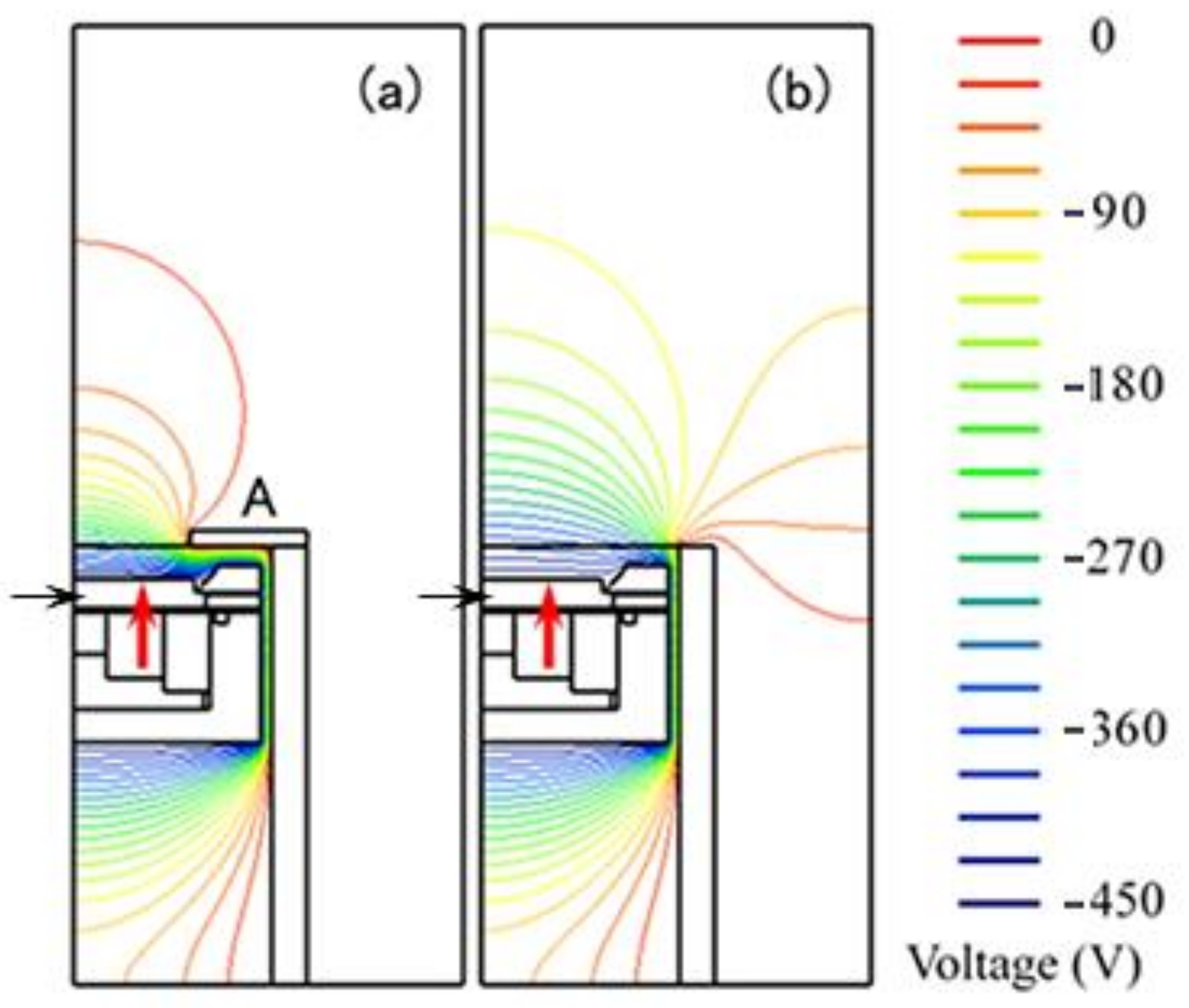
2. Materials and Methods

The experimental setup has been described in detail in previous studies [44]. The vacuum chamber was pumped by a turbo molecular pump (Edwards, STP-A2203C) to be a base pressure on the order of 10−6 Pa. Argon gas (99.999%) was introduced into the chamber using a mass flow controller (Kofloc, CR-400). The operating pressure was set to be in the range of 0.32 to 1.55 Pa. The argon flow rate for the pressure range was in the range of 100 to 1200 sccm. A commercial circular unbalanced magnetron (Gencoa, Circular VTech) as a sputtering source was equipped with a titanium target (diameter: 2 in.).
The anode shape of the sputtering source is an important factor to observe discharge ignition and delayed discharge with sputtering. Figure 1 shows right-side cross sections of the planar magnetron and electric potential distributions calculated by an axisymmetric model as the sputtering source in the range of target voltage from 0 to 450 V using a finite-element-method electromagnetic field analysis simulator (Mutec, μ-Excel). Two grounded anode shapes were examined by the simulator: a grounded anode shape with a flat, ring-shaped shield (A) (Figure 1a) and a grounded anode shape without a flat, ring-shaped shield (Figure 1b). As shown by the density of electric potential distributions in Figure 1, the gradient of the electric field formed near the target for the sputtering source without the anode shield was lower than that with the anode shield. The results of the electric field analysis for the area from the target surface up to approximately 10 mm at the erosion position of the target, as indicated by red arrows in Figure 1, suggest that the electric field with the anode shield is approximately doubled compared to that without the anode shield. As shown in Figure 1b, the ring-shaped shield of the anode was removed from the sputtering source in the present study in order to minimize the density of electric potential distributions.
A high-power pulse generator (Zpulser, AxiaTM) used as the power supply for the MPPMS system was used to set a repetition rate of 20 Hz. The waveform of the micro-pulse train, which is used to control the insulated gate bipolar transistor in the pulse generator chopping the charging voltage, is shown in Figure 2. The micro-pulses and the segments designed by pulse-on times and pulse-off times are summarized in Table 1.

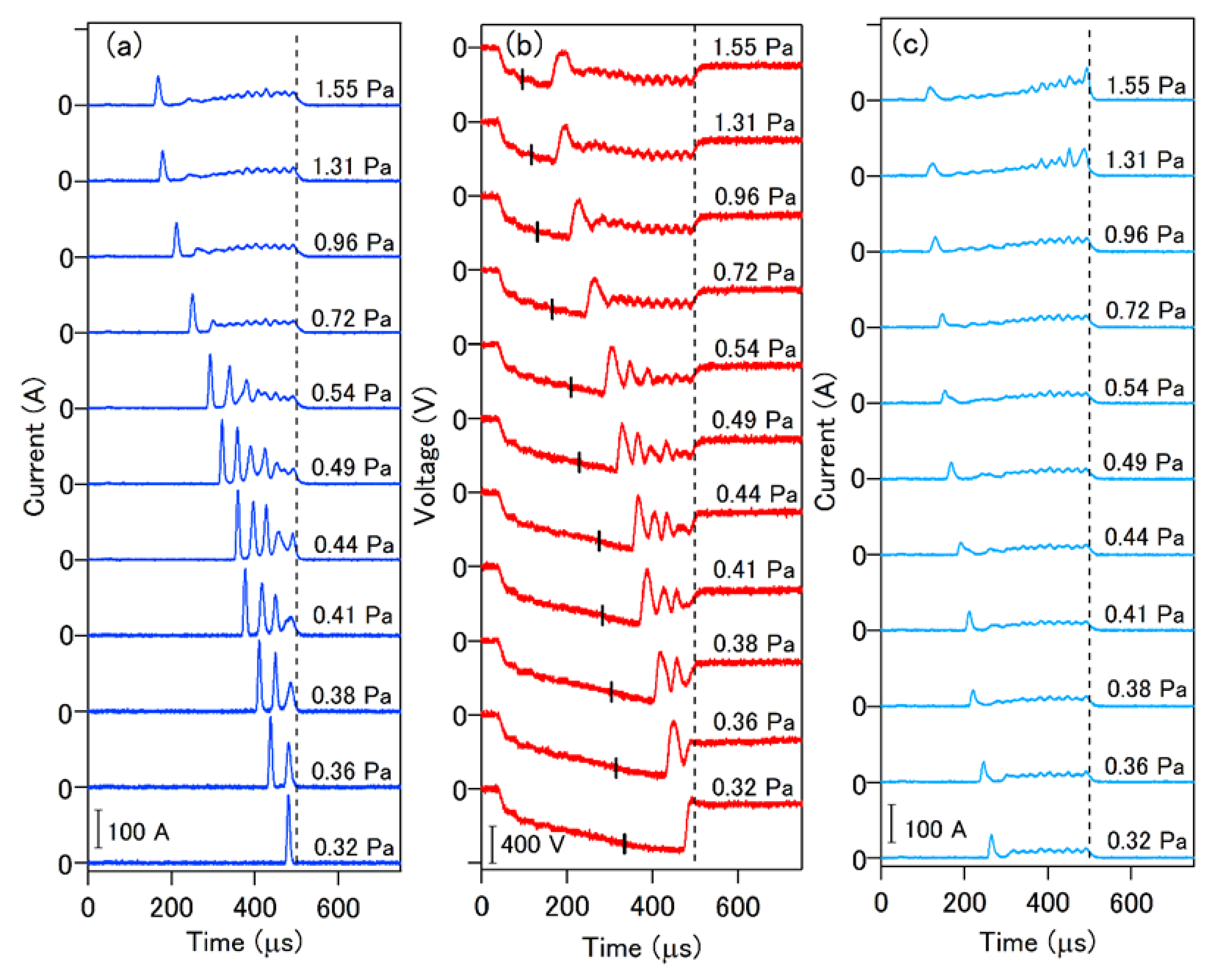
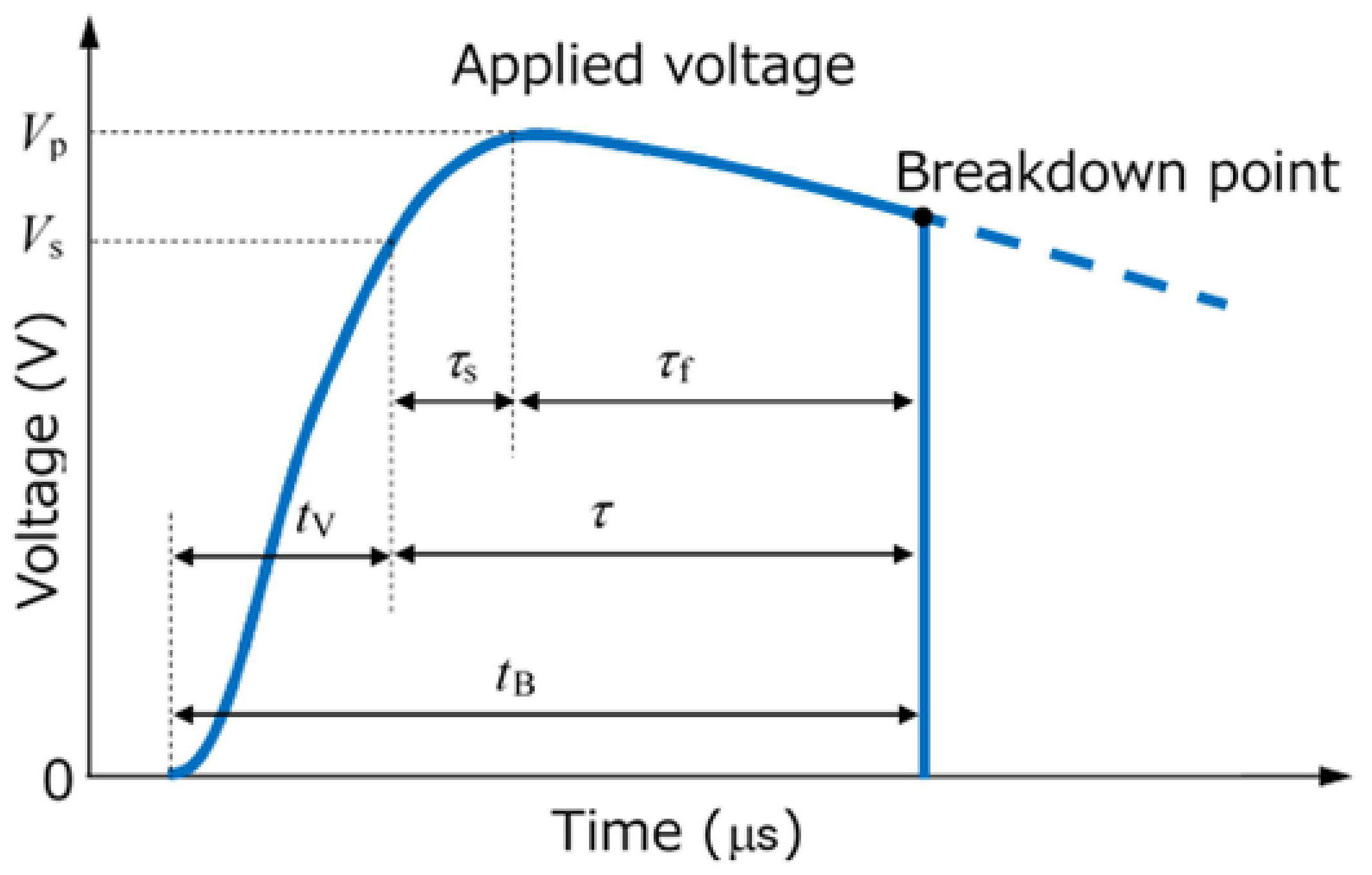
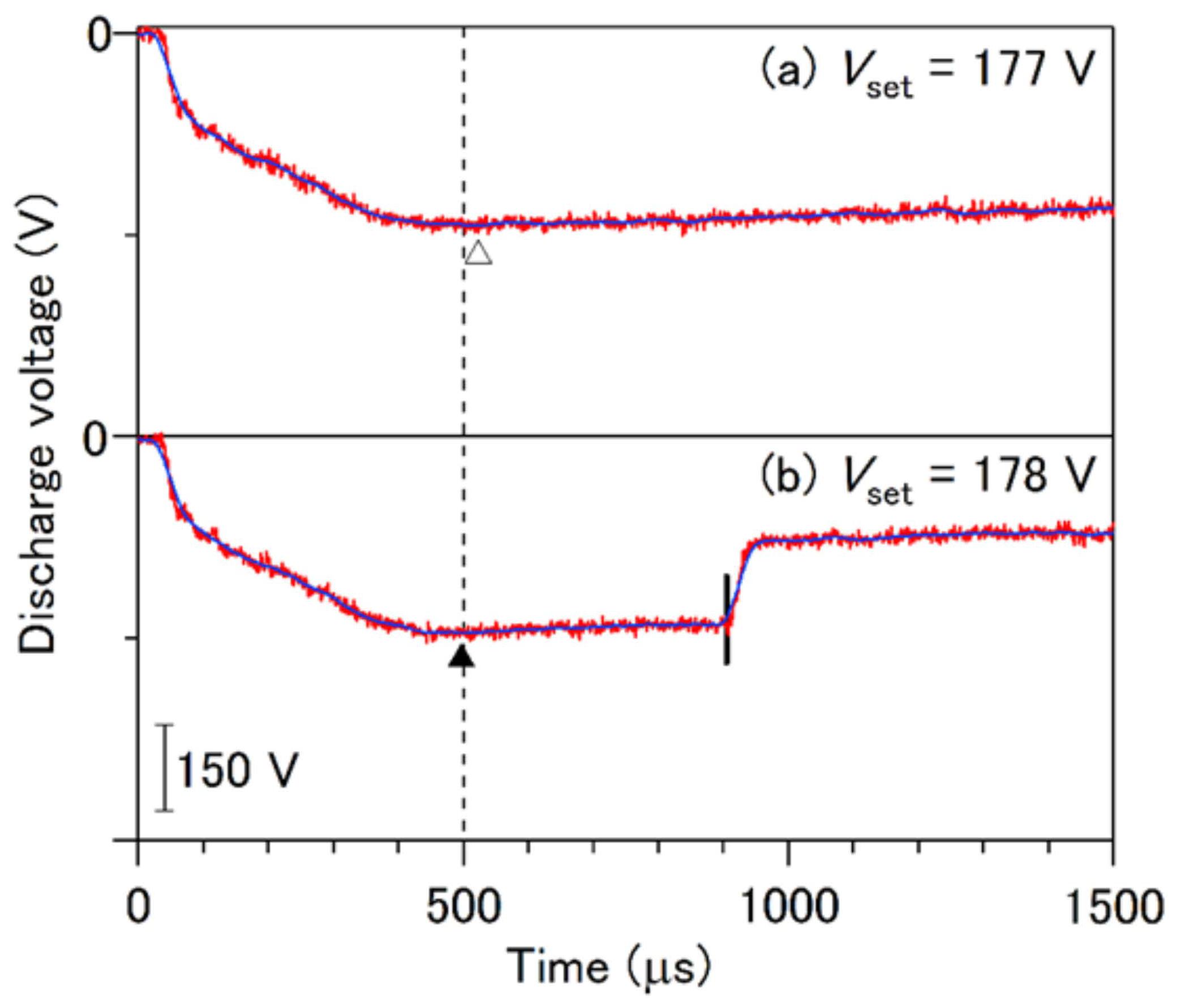
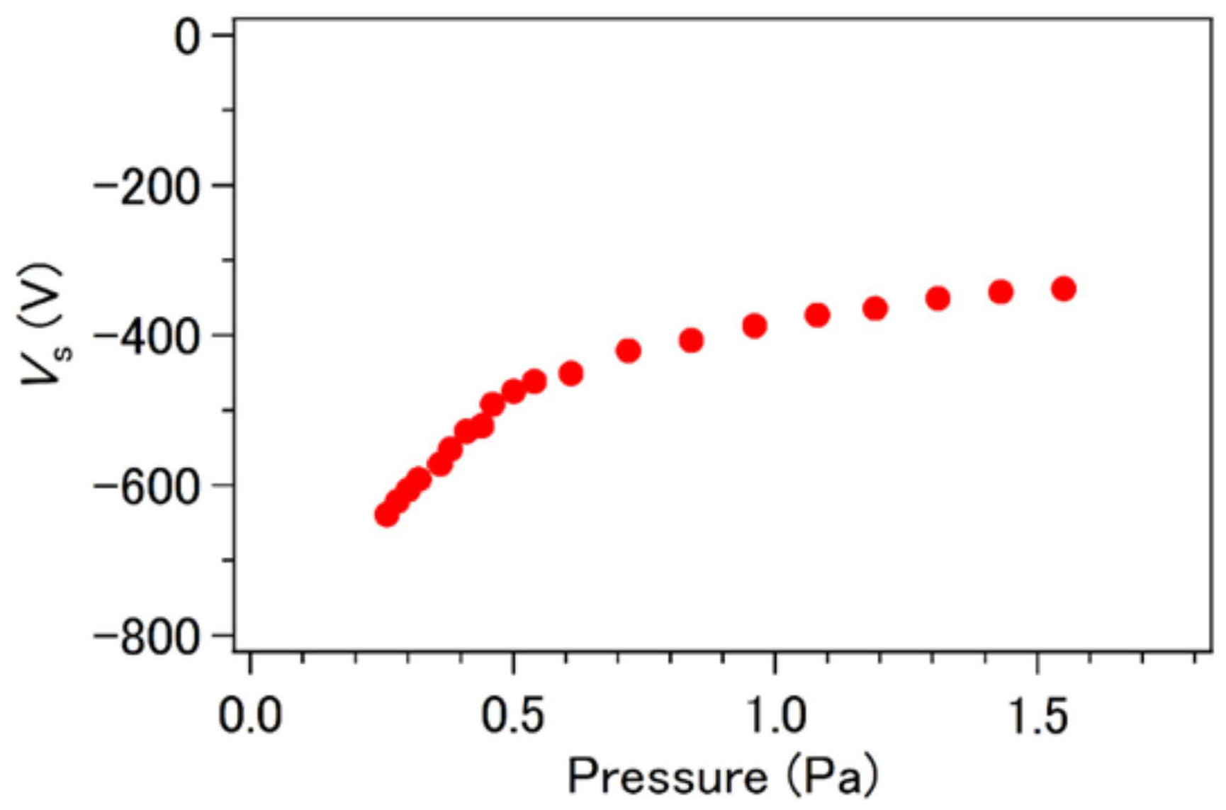
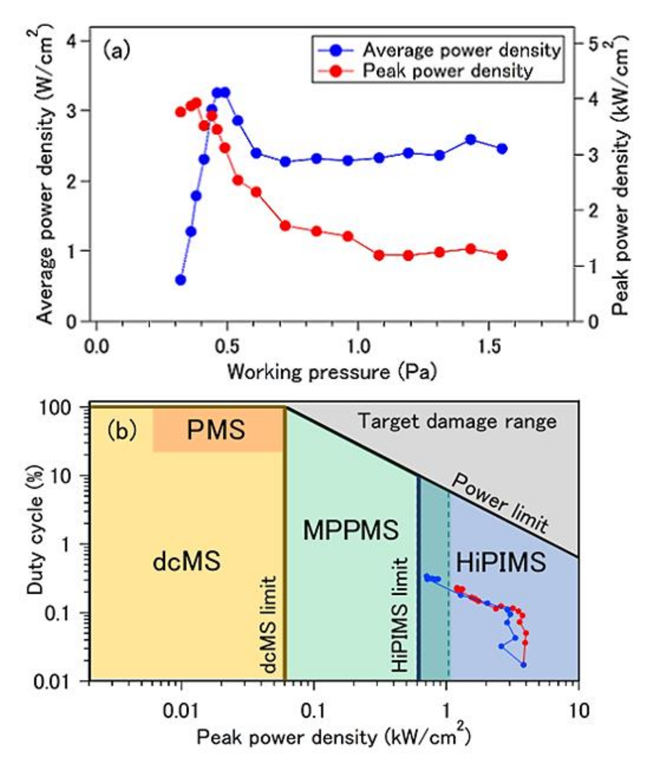
3. Results and Discussion

Figure 3 shows the waveforms of the discharge current and discharge voltage in the working pressure range of 0.32 to 1.55 Pa. The pressure range in which the waveform change can be observed is lower than 0.81 to 1.60 Pa. This is due to the replacement of magnets that have been thermally damaged by maintenance of the sputtering source. The new magnets are thought to have increased the density of magnetron electrons near the target, enabling discharge even at lower pressures.
As shown in Figure 3a, the evolution of the current waveform revealed that the onsets of current were remarkably delayed. This phenomenon is referred to as delayed discharge and was observed prominently for the first time in MPPMS plasma of titanium. The breakdown of discharge voltage was also observed with same timing for the rise of the discharge current at the same gas pressure, as shown in Figure 3b. As the argon pressure decreased, the current waveform was divided into several pulses, generating a comb-like current waveform [32], and the current waveform then became a single pulse with a high peak current at 0.32 Pa. The comb-like current waveform observed in the working pressure range of 0.32 to 0.54 Pa was similar to the discharge current waveform in DOMS [16]. The time interval between peaks of the comb-like current waveform was the same as that of the micro-pulses of the MPP power supply. For the 0.41-Pa discharge, however, the pulse interval (approximately 40 μs) in the comb-like current waveform was several times longer than the OFF times between micro-pulses (10 μs). This difference may be determined by the electrical time constant inside the MPP power supply. In addition, a remarkable delay (as long as approximately 500 μs), which corresponded to the power pulse width, was observed with the increase of the discharge current at the lowest argon pressure.
The delayed discharge originates from the electrical breakdown (ignition). The onset and voltage waveform of delayed discharges are shown in Figure 4 [36]. Whether electrical breakdown occurs and the degree of the time lag from the applied point of charging voltage are explained by Townsend’s discharge theory formula. According to Townsend’s discharge theory, the ionization coefficient α is given as follows [36,37]:
α = A p exp B E p ,
where A and B are constant values, E is the electric field, and p is the pressure. As noted in Section 2, the electric field E is approximately half that for the case without the anode shield (as compared to the case with the anode shield), and as a result, the value of α is exp (−2) = 0.14 times. From Equation (1), if the electric field is low under a constant pressure, then the initial discharge is less likely to occur due to the small ionization coefficient. Thus, the extent of the delayed discharge is strongly affected by the electric field in front of the target and the ionization factor, which are sensitively dependent on the anode shape with and without the anode shield. As shown in Figure 3c, the discharge with the anode shield showed delayed discharges, but the observed delay time was as small as approximately half that without the anode shield, and no comb-like discharge current waveform was observed. As a result, sputtering sources without anode shields made it easier to observe significant delayed discharges and comb-like discharge current waveforms as compared to sputtering sources with anode shields. Therefore, the sputtering source without the anode shield, as shown in Figure 1b, was intentionally used in order to observe the sputtering plasma with the delayed discharges in the present study.
Assuming that the applied voltage is V and the mean free path of an electron, which corresponds to the electrode spacing of the MPPMS device before ionization collision, is d, then the electric field E in Equation (1) can be rewritten as follows using the relationship E = V/d [36,37]:
α = A p exp B p d V
According to Paschen’s law using the Townsend’s formula, the minimum breakdown voltage Vs is given as follows [36,37]:
V S = B p d ln A p α .
If the mean free path of electrons is longer than the mean free path between electrodes, then d is the constant electrode gap. In contrast, if the mean free path of electrons is shorter than the mean free path between electrodes, then d is the mean free path of electrons. The former case may be applicable for lower pressure and voltage measurements, and the latter case may be applicable for higher pressure and voltage measurements [38].
As shown in Figure 4, for the breakdown and delay time under the impulse voltage [36], the delay time τ for electrical breakdown is written as [37]:
τ = t B t V ,  
where tB is the time at breakdown and tV is the time at the minimum breakdown voltage Vs. In terms of breakdown characteristics, the delay time τ starts from the time for Vs and is defined as the sum of the statistical time τs, which is the time until the first seed electron appears, and the formative time τf, which is the time required for the electrical breakdown to develop from the first seed electron in addition to the time required to wait for the sheath formation and the discharge development [36,37,42,45]:
τ = τ s + τ f .
Therefore, in order to obtain τ experimentally, it is necessary to observe Vs and then determine the starting point of τ. Figure 5 shows (a) the non-discharge voltage waveform at the highest charging voltage (Vset = 177 V) and (b) the discharge voltage waveform at the lowest charging voltage (Vset = 178 V) measured at 1.55 Pa by adjusting the charging voltage (adjustment limit: 1 V) of the MPP power supply. Assuming that there is a true Vs between the maximum voltages in each voltage waveform, −334 V for Vset = 177 V and −341 V for Vset = 178 V, then Vs can be determined experimentally as the average of these values. The maximum voltage difference observed was less than 10 V. Figure 6 shows the value of Vs obtained as a function of argon pressure using this method.
The delay time τ can be obtained as the interval time between the times of Vs and the breakdown point by plotting the measured Vs on the observed discharge voltage waveforms, as shown in Figure 3a. Furthermore, the two components (τs and τf) of the delay time τ can be determined from a Laue plot for the delay time [35]. The delay time follows the statistical law of change. For the total number of trials N, if the number of trials for which the measured delay time is longer than the statistically true delay time τ is written as n, then the cumulative frequency n/N (%) is expressed as a function of delay time as follows [35,36]:
n N = 100 · exp t τ f τ s .
A typical example of a Laue plot for the discharge at the working pressure of 0.41 Pa is shown in Figure 7. The tv required to determine the delay time τ was the time at which Vs = −528 V as measured in the experiment. As a result of fitting of the experimental data to the function of n/N (%) = 100∙exp[−(t [μs] − X)/Y], the parameters X and Y were determined to be 91.4 μs and 5.51 μs as a major discharge component and 94.0 μs and 1.44 μs as a minor discharge component for N = 25, as shown in Figure 7. In both discharges, it was experimentally confirmed that τs was approximately 10% of the τf. The ratio between the lengths of these delay times is consistent with the trend of general electric breakdown.
In addition, the origin of the major and minor discharges is due to discharge fluctuations that occur within half of the pulse-off time (10 μs) at the breakdown point, considering the time difference (approximately 3 μs) between two formative times. Figure 8 shows Laue plots measured at several argon pressures at which characteristic discharge current waveforms are observed: 1.55 and 0.72 Pa, at which typical MPPMS current waveforms are observed; 0.44 Pa, at which a current waveform consisting of five pulses is observed; 0.41 Pa, at which a current waveform consisting of four pulses is observed; 0.38 Pa, at which a current waveform consisting of three pulses is observed; 0.36 Pa, at which a current waveform consisting of two pulses is observed; and 0.32 Pa, at which a current waveform consisting of a single pulse is observed. This figure shows that τf strongly depends on argon pressure, and that the 1.55-Pa Laue plot clearly jumps to the 0.72-Pa Laue plot in the slower time region. The latter behavior is also explained as the discharge fluctuation for the minor discharge.
Furthermore, τf and τs for components of these major and minor discharges obtained by fitting calculations for the Laue plots at each pressure are plotted in Figure 9 and summarized in Table 2. These results also confirmed that τf >> τs in MPPMS, as mentioned in a previous paper on HiPIMS [38]. Comparing the major and minor discharges as a feature of τf, the value of the major discharge was several microseconds shorter than the value of the minor discharge. On the other hand, as a feature of τs, the value of the major discharge was several microseconds longer than the value of the minor discharge. This suggests that the after-glow plasma (i.e., pre-ionized plasma [11,42,43]) made by major pulsed discharges shortens time τs of the minor discharges [41]. It has been reported that τs is lower than 2 μs in HiPIMS of copper [42]. τs’s in the major and minor discharges of titanium were the same-order value to τs of copper. This is because the secondary electron yields of these target metals (copper and titanium) are the same order value [46,47].
Although the breakdown time of HiPIMS [34], its discharge voltage dependence [38,39], and its working pressure dependence [38] have been reported, there has been no report on the gas pressure dependence of the delay time in both HiPIMS and MPPMS. Assuming that pd < 1 in the low-pressure condition, the delay time τ is approximated as [38,48]:
τ a V s 2 p d 2 Δ V ,
where a is a constant, and ΔV is the overvoltage for the breakdown as given by ΔV = VPVS. The obtained result also shows that the statistical time is much smaller than the formative time (τs << τf). Therefore, the delay time τ is approximately equal to the formative time ττf because the formative time accounts for most of the delay time.
However, assuming that d is constant, Equation (7) cannot be optimized for τf (major), especially in the pressure range over 0.6 Pa. On the other hand, pd is assumed to be constant in Equation (7), because d is considered to be the mean path of electrons that are inversely proportional to p in higher-voltage measurements [38]. Thus, the following equation is obtained:
τ f a V s 2 Δ V .
As shown in Figure 9, the experimental data was fit to the formula (τ [μs]) = (AVsΔV−1 [V]), wherein the value of parameter A was determined to be 2.35 × 10⁻². The fitting results were good enough, except at 1.55 Pa. This result means that the voltage factor (Vs2V) in Equation (7) determines the delay times in this MPPMS discharge.
Figure 10a shows the peak current and peak voltage in the working pressure range of 0.32 to 1.55 Pa in the present study. In particular, the peak current increases with the increase in accumulated charges that participate in the ignition due to the delay effect with decreasing argon pressure. In addition, the formation of the comb-like discharge current waveforms in Figure 3a steeply increases the average power density.
According to the duty-cycle diagram for magnetron sputtering depicted by Gudmundsson et al. [1], the peak power of the HiPIMS region is defined as exceeding 0.6 kW/cm2. Finally, the peak power densities for observed discharge current and voltage waveforms were plotted on Gudmundsson’s diagram as shown in Figure 10b. The optional plot, except for the first pulse, which is less involved in sputtering, as shown in the OES study [32], also shows that the power waveform to the comb-like current and voltage waveforms exhibits high peak power densities. Figure 10b, which summarizes the results extracted from the power waveform in our study, shows that the peak power density shifted from the MPPMS region to the HiPIMS region with delayed discharge, and that the duty ratio steeply dropped according to the number of pulses and from the point where the comb-like power waveform used in DOMS was formed. This result may be a minor aspect of plasma manipulation using MPP power supplies.
However, as reported in our study on OES of comb-like discharge current waveforms, the pulses with large power contained in the comb-like power waveform formed by adjusting the argon gas pressure have a technical potential in order to increase the flux of ionized sputtered particles and generate MPPMS plasma with a higher ionization degree [32]. The findings obtained in the present study provide a new perspective in modulated pulse design for I-PVD using DOMS.

4. Conclusions

The delayed discharge behavior observed using a sputtering source without an anode shield in MPPMS plasma of titanium was investigated through argon pressure dependence for discharge current waveforms. We have found that the discharge current waveform changes from typical MPPMS discharge current waveforms to comb-like DOMS discharge current waveforms containing several pulses as the argon pressure decreases. The MPP discharge dynamics based on the measurements of true discharge delay times (τf and τs), which would be the key to the formation of DOMS discharge current waveforms, were reported in the present study.

Author Contributions

Conceptualization, M.S.; methodology, M.S.; validation, M.S., H.N. and T.W.; formal analysis, M.S. and H.N.; investigation, M.S., H.N., T.W., Y.N. and Y.H.; data curation, M.S.; writing—original draft preparation, M.S.; writing—review and editing, M.S., N.N., M.T., H.Y., N.H, K.T., K.O., F.M. and K.F.; supervision, N.N., F.M. and K.F.; funding acquisition, M.S., M.T., N.H., H.Y., K.T., K.O., F.M. and K.F. All authors have read and agreed to the published version of the manuscript.

Funding

This work was supported by New Aichi creative research and development grants 2017 (Grant No. 118-9, Industry and Science Technology Division 29), 2018 (Grant No. 122-10, Industry and Science Technology Division 30) from Aichi prefecture, Japan, manufacturing enterprise promotion business grants-in-aid of research and development 2019 (Grant No. 65-2) and 2020 (Grant No. 65-1) from Anjo City, Japan, and a Grant-in-Aid for Scientific Research from the Japan Society for the Promotion of Science (JSPS) 2021 (Grant No. 21K03503).

Data Availability Statement

The data presented in this study are available on request from the corresponding author.

Conflicts of Interest

The authors declare no conflict of interest.

References

  1. Gudmundsson, J.T.; Brenning, N.; Lundin, D.; Helmersson, U. High power impulse magnetron sputtering discharge. J. Vac. Sci. Technol. A 2012, 30, 030801. [Google Scholar] [CrossRef] [Green Version]
  2. Lin, J.; Moore, J.J.; Sproul, W.D.; Mishra, B.; Wu, Z. Modulated pulse power sputtered chromium coatings. Thin Solid Films 2009, 518, 1566–1570. [Google Scholar] [CrossRef]
  3. Lin, J.; Moore, J.; Sproul, W.; Mishra, B.; Rees, J.; Wu, Z.; Chistyakov, R.; Abraham, B. Ion energy and mass distributions of the plasma during modulated pulse power magnetron sputtering. Surf. Coat. Technol. 2009, 203, 3676–3685. [Google Scholar] [CrossRef]
  4. Lin, J.; Moore, J.J.; Sproul, W.D.; Mishra, B.; Wu, Z.; Wang, J. The structure and properties of chromium nitride coatings deposited using dc, pulsed dc and modulated pulse power magnetron sputtering. Surf. Coat. Technol. 2010, 204, 2230–2239. [Google Scholar] [CrossRef]
  5. Lin, J.; Moore, J.J.; Sproul, W.D.; Lee, S.L.; Wang, J. Effect of Negative Substrate Bias on the Structure and Properties of Ta Coatings Deposited Using Modulated Pulse Power Magnetron Sputtering. IEEE Trans. Plasma Sci. 2010, 38, 3071–3078. [Google Scholar] [CrossRef]
  6. Liebig, B.; Braithwaite, N.S.J.; Kelly, P.; Chistyakov, R.; Abraham, B.; Bradley, J. Time-resolved plasma characterisation of modulated pulsed power magnetron sputtering of chromium. Surf. Coat. Technol. 2011, 205, S312–S316. [Google Scholar] [CrossRef]
  7. Papa, F.; Gerdes, H.; Bandorf, R.; Ehiasarian, A.; Kolev, I.; Braeuer, G.; Tietema, R.; Krug, T. Deposition rate characteristics for steady state high power impulse magnetron sputtering (HIPIMS) discharges generated with a modulated pulsed power (MPP) generator. Thin Solid Films 2011, 520, 1559–1563. [Google Scholar] [CrossRef]
  8. Hála, M.; Čapek, J.; Zabeida, O.; Klemberg-Sapieha, J.; Martinu, L. Pulse management in high power pulsed magnetron sputtering of niobium. Surf. Coat. Technol. 2012, 206, 4186–4193. [Google Scholar] [CrossRef]
  9. Hála, M.; Capek, J.; Zabeida, O.; Klemberg-Sapieha, J.E.; Martinu, L. Hysteresis-free deposition of niobium oxide films by HiPIMS using different pulse management strategies. J. Phys. D Appl. Phys. 2012, 45, 055204. [Google Scholar] [CrossRef]
  10. Zheng, B.C.; Wu, Z.L.; Wu, B.; Li, Y.G.; Lei, M.K. A global plasma model for reactive deposition of compound films by modulated pulsed power magnetron sputtering discharges. J. Appl. Phys. 2017, 121, 171901. [Google Scholar] [CrossRef]
  11. Helmersson, U.; Lattemann, M.; Bohlmark, J.; Ehiasarian, A.P.; Gudmundsson, J.T. Ionized physical vapor deposition (IPVD): A review of technology and applications. Thin Solid Films 2006, 513, 1–24. [Google Scholar] [CrossRef] [Green Version]
  12. Sarakinos, K.; Alami, J.; Konstantinidis, S. High power pulsed magnetron sputtering: A review on scientific and engineering state of the art. Surf. Coat. Technol. 2010, 204, 1661–1684. [Google Scholar] [CrossRef]
  13. Britun, N.; Minea, T.; Konstantinidis, S.; Snyders, R. Plasma diagnostics for understanding the plasma–surface interaction in HiPIMS discharges: A review. J. Phys. D Appl. Phys. 2014, 47, 224001. [Google Scholar] [CrossRef] [Green Version]
  14. Anders, A. Tutorial: Reactive high-power impulse magnetron sputtering (R-HiPIMS). J. Appl. Phys. 2017, 121, 171101. [Google Scholar] [CrossRef] [Green Version]
  15. Hopwood, J.A. Thin Films Vol. 27: Ionized Physical Vapor Deposition; Hopwood, J.A., Ed.; Academic Press: San Diego, CA, USA, 2000; pp. 181–207. [Google Scholar]
  16. Lin, J.; Wang, B.; Sproul, W.D.; Ou, Y.; Dahan, I. Anatase and rutile TiO2 films deposited by arc-free deep oscillation magnetron sputtering. J. Phys. D Appl. Phys. 2013, 46, 84008. [Google Scholar] [CrossRef]
  17. Lin, J.; Sproul, W.D.; Wei, R.; Chistyakov, R. Diamond like carbon films deposited by HiPIMS using oscillatory voltage pulses. Surf. Coat. Technol. 2014, 258, 1212–1222. [Google Scholar] [CrossRef]
  18. Ferreira, F.; Serra, R.; Oliveira, J.; Cavaleiro, A. Effect of peak target power on the properties of Cr thin films sputtered by HiPIMS in deep oscillation magnetron sputtering (DOMS) mode. Surf. Coat. Technol. 2014, 258, 249–256. [Google Scholar] [CrossRef]
  19. Lin, J.; Sproul, W.D. Structure and properties of Cr2O3 coatings deposited using DCMS, PDCMS, and DOMS. Surf. Coat. Technol. 2015, 276, 70–76. [Google Scholar] [CrossRef]
  20. Ou, Y.; Lin, J.; Tong, S.; Che, H.; Sproul, W.D.; Lei, M. Wear and corrosion resistance of CrN/TiN superlattice coatings deposited by a combined deep oscillation magnetron sputtering and pulsed dc magnetron sputtering. Appl. Surf. Sci. 2015, 351, 332–343. [Google Scholar] [CrossRef]
  21. Ferreira, F.; Oliveira, J.; Cavaleiro, A. CrN thin films deposited by HiPIMS in DOMS mode. Surf. Coat. Technol. 2016, 291, 365–375. [Google Scholar] [CrossRef]
  22. Oliveira, J.; Fernandes, F.; Serra, R.; Cavaleiro, A. On the role of the energetic species in TiN thin film growth by reactive deep oscillation magnetron sputtering in Ar/N2. Thin Solid Films 2018, 645, 253–264. [Google Scholar] [CrossRef]
  23. Ferreira, F.; Aijaz, A.; Kubart, T.; Cavaleiro, A.; Oliveira, J. Hard and dense diamond like carbon coatings deposited by deep oscillations magnetron sputtering. Surf. Coat. Technol. 2018, 336, 92–98. [Google Scholar] [CrossRef]
  24. Oliveira, J.C.; Ferreira, F.; Anders, A.; Cavaleiro, A. Reduced atomic shadowing in HiPIMS: Role of the thermalized metal ions. Appl. Surf. Sci. 2018, 433, 934–944. [Google Scholar] [CrossRef]
  25. Antonin, O.; Tiron, V.; Costin, C.; Popa, G.; Minea, T.M. On the HiPIMS benefits of multi-pulse operating mode. J. Phys. D Appl. Phys. 2015, 48, 015202. [Google Scholar] [CrossRef]
  26. Fekete, M.; Hnilica, J.; Vitelaru, C.; Minea, T.; Vašina, P. Ti atom and Ti ion number density evolution in standard and multi-pulse HiPIMS. J. Phys. D Appl. Phys. 2017, 50, 365202. [Google Scholar] [CrossRef]
  27. Tiron, V.; Velicu, I.-L.; Dobromir, M.; Demeter, A.; Samoila, F.; Ursu, C.; Sirghi, L. Reactive multi-pulse HiPIMS deposition of oxygen-deficient TiOx thin films. Thin Solid Films 2016, 603, 255–261. [Google Scholar] [CrossRef]
  28. Tiron, V.; Velicu, I.-L.; Mihǎilǎ, I.; Popa, G. Deposition rate enhancement in HiPIMS through the control of magnetic field and pulse configuration. Surf. Coat. Technol. 2018, 337, 484–491. [Google Scholar] [CrossRef]
  29. Tiron, V.; Ursu, E.-L.; Cristea, D.; Munteanu, D.; Bulai, G.; Ceban, A.; Velicu, I.-L. Overcoming the insulating materials limitation in HiPIMS: Ion-assisted deposition of DLC coatings using bipolar HiPIMS. Appl. Surf. Sci. 2019, 494, 871–879. [Google Scholar] [CrossRef]
  30. Hnilica, J.; Klein, P.; Vašina, P.; Snyders, R.; Britun, N. Revisiting particle dynamics in HiPIMS discharges. I. General effects. J. Appl. Phys. 2020, 128, 043303. [Google Scholar] [CrossRef]
  31. Hnilica, J.; Klein, P.; Vašina, P.; Snyders, R.; Britun, N. Revisiting particle dynamics in HiPIMS discharges. II. Plasma pulse effects. J. Appl. Phys. 2020, 128, 043304. [Google Scholar] [CrossRef]
  32. Sanekata, M.; Nishida, H.; Nakagomi, Y.; Hirai, Y.; Nishimiya, N.; Tona, M.; Hirata, N.; Yamamoto, H.; Tsukamoto, K.; Ohshimo, K.; et al. to be submitted to Plasma.
  33. Musil, J.; Leština, J.; Vlček, J.; Tölg, T. Pulsed dc magnetron discharge for high-rate sputtering of thin films. J. Vac. Sci. Technol. A 2001, 19, 420–424. [Google Scholar] [CrossRef]
  34. Gudmundsson, J.; Alami, J.; Helmersson, U. Spatial and temporal behavior of the plasma parameters in a pulsed magnetron discharge. Surf. Coat. Technol. 2002, 161, 249–256. [Google Scholar] [CrossRef]
  35. Von Engel, A. Ionized Gases; American Vacuum Society Classics; American Institute of Physics: New York, NY, USA, 1994; pp. 204–212. [Google Scholar]
  36. Kuffel, E.; Zaengl, W.; Kuffel, J. High Voltage Engineering Fundamentals; Elsevier BV: Amsterdam, The Netherlands, 2000; pp. 383–391. [Google Scholar]
  37. Raizer, Y.P. Gas Discharge Physics; Allen, J.E., Ed.; Springer: New York, NY, USA, 1991; pp. 52–56, 128–137. [Google Scholar]
  38. Yushkov, G.Y.; Anders, A. Origin of the Delayed Current Onset in High-Power Impulse Magnetron Sputtering. IEEE Trans. Plasma Sci. 2010, 38, 3028–3034. [Google Scholar] [CrossRef] [Green Version]
  39. Nakano, T.; Murata, C.; Baba, S. Effect of the target bias voltage during off-pulse period on the impulse magnetron sputtering. Vacuum 2010, 84, 1368–1371. [Google Scholar] [CrossRef]
  40. Zuo, X.; Chen, R.; Ke, P.; Wang, A. Gas Breakdown and Discharge Formation in High-Power Impulse Magnetron Sputtering. IEEE Trans. Plasma Sci. 2019, 47, 1215–1222. [Google Scholar] [CrossRef]
  41. Han, M.; Luo, Y.; Li, H.; Li, L.; Xu, Y.; Luo, S.; Zhang, P.; Xu, H.; Xu, C. Auxiliary capacitor to enhance oscillation in circuit and reduce current onset delay in HiPIMS discharge: Theory, experiment and simulation. Surf. Coat. Technol. 2021, 405, 126518. [Google Scholar] [CrossRef]
  42. Vašina, P.; Meško, M.; Imbert, J.C.; Ganciu, M.; Boisse-Laporte, C.; De Poucques, L.; Touzeau, M.; Pagnon, D.; Bretagne, J. Experimental study of a pre-ionized high power pulsed magnetron discharge. Plasma Sour. Sci. Technol. 2007, 16, 501–510. [Google Scholar] [CrossRef]
  43. Mozgrin, D.V.; Fetisov, I.K.; Khodachenko, G.V. High-current low-pressure quasi-stationary discharge in a magnetic field: Experimental research. Plasma Phys. Rep. 1995, 21, 422. [Google Scholar]
  44. Tsukamoto, K.; Tamura, T.; Matsusaki, H.; Tona, M.; Yamamoto, H.; Nakagomi, Y.; Nishida, H.; Hirai, Y.; Nishimiya, N.; Sanekata, M.; et al. Time-of-flight mass spectrometric diagnostics for ionized and neutral species in high-power pulsed magnetron sputtering of titanium. Jpn. J. Appl. Phys. 2020, 59, SHHB05. [Google Scholar] [CrossRef]
  45. Kudrle, V.; LeDuc, E.; Fitaire, M. Breakdown delay times and memory effects in helium at low pressure. J. Phys. D Appl. Phys. 1999, 32, 2049–2055. [Google Scholar] [CrossRef] [Green Version]
  46. Phelps, A.V.; Petrović, Z.L. Cold-cathode discharges and breakdown in argon: Surface and gas phase production of secondary electrons. Plasma Sour. Sci. Technol. 1999, 8, R21–R44. [Google Scholar] [CrossRef] [Green Version]
  47. Walker, C.G.H.; El-Gomati, M.M.; Assa’d, A.M.D.; Assa’d, A.M.D. The secondary electron emission yield for 24 solid elements excited by primary electrons in the range 250-5000 ev: A theory/experiment comparison. Scanning 1999, 32, 2049–2055. [Google Scholar] [CrossRef] [PubMed]
  48. Schade, R. Über die Aufbauzeit einer Glimmentladung. Z. Phys. 1937, 104, 487–510. [Google Scholar] [CrossRef]
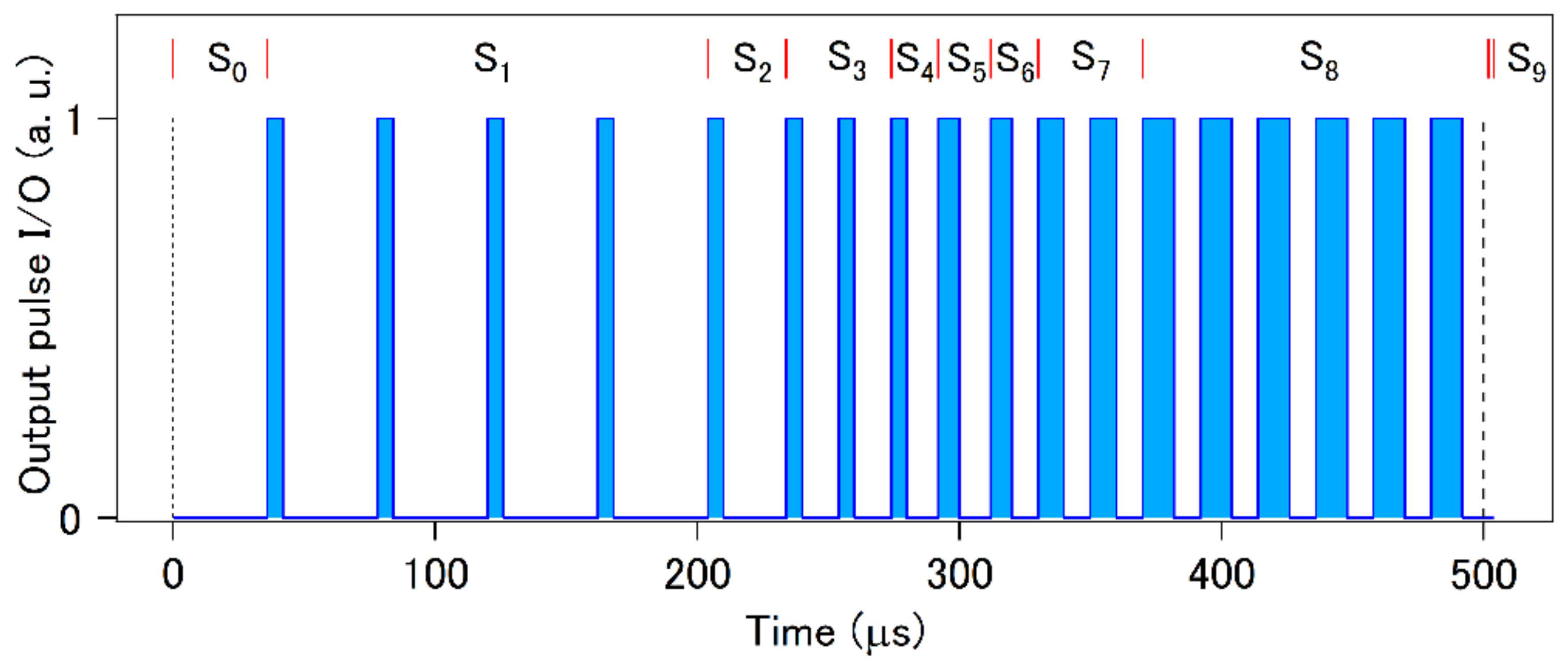
Figure 1. Right-side cross sections of a planar magnetron and electric potential distributions calculated by an axial target model using a finite-element-method electromagnetic field analysis simulator (Mutec, μ-Excel) as the sputtering source. Grounded anode structures (a) with a flat, ring-shaped shield (standard type) and (b) without a flat, ring-shaped shield. The black and red arrows indicate the target and the erosion position of the target, respectively. The calculated results exclude the indication of the potentials of target and the magnetron for clarity.
Plasma 04 00016 g001
Figure 2. Micro-pulse train waveform (blue bars) and segments designed based on the pulse-on times and pulse-off times for the micro-pulses summarized in Table 1. The pulsed power is output based on the micro-pulse train waveform.
Plasma 04 00016 g002
Figure 3. (a) Discharge current waveforms (blue lines) and (b) discharge voltage waveforms (red lines) in modulated pulsed power magnetron sputtering (MPPMS) for the working pressure in the range of 0.32 to 1.55 Pa. The black dashed lines indicate the cutoff time of pulsed power, which is output from a high-power pulsed generator. The short black lines on the discharge current waveforms indicate the breakdown voltage Vs as a function of argon pressure. (c) Discharge current waveforms (light blue lines) for MPPMS with an anode ring, as shown in Figure 1a.
Plasma 04 00016 g003
Figure 4. Typical breakdown and time lag under impulse voltage. Here, Vp and Vs are peak voltage and minimum breakdown voltage, respectively, and tB and tv are the breakdown time and the time when the charge voltage exceeds Vs, respectively. Moreover, τ, τs, and τf are the delay time, the statistical time, and formative time, respectively [36].
Plasma 04 00016 g004
Figure 5. Voltage waveforms measured to determine values of Vs in MPPMS discharged for two different values of Vset at a working pressure of 1.55 Pa. The black dashed line indicates the cutoff time of pulsed power, which is output from the high-power pulsed generator. (a) Maximum voltage waveform with no observed discharge at Vset = 177 V. The blue lines on the voltage waveforms depicted by red lines are the smoothed voltage waveforms for reading the maximum voltages. The open triangle represents the maximum charge voltage in the voltage waveform. (b) Minimum voltage waveform with observed discharge at Vset = 178 V. The solid triangle represents the maximum charge voltage in the voltage waveform. The short black line indicates the time of electrical breakdown occurring after the cutoff time of pulsed power. The value of Vs is approximately determined as the average of the voltages indicated by the two triangles. The resulting Vs obtained in the present study show a small change as a function of pressure as compared to the calculated values [41].
Plasma 04 00016 g005
Figure 6. Breakdown voltage Vs as a function of the working pressure in MPPMS for working pressure in the range of 0.32 to 1.55 Pa.
Plasma 04 00016 g006
Figure 7. Typical Laue plot for the electrical breakdowns at 0.41 Pa for the working pressure and at Vs = −528 V (red solid circles). The fitting results (n/N [%]) = 100e−(t − 91.4 [μs])/5.51 [μs] as a major discharge component and 61.5e−(t − 94.0 [μs])/1.44 [μs] as a minor discharge component for N = 25 are indicated by the blue and green dashed lines, respectively. The times (τf) of major and minor discharges are also indicated.
Plasma 04 00016 g007
Figure 8. Laue plots for the electrical breakdowns of N = 25 in MPPMS for the working pressure in the range of 0.32 to 1.55 Pa.
Plasma 04 00016 g008
Figure 9. Formative times τf (solid circles) and statistical times τs (open circles) in MPPMS discharge as a function of argon pressure in the range of 0.32 to 1.55 Pa. The major and minor components are colored blue and green, respectively. Maximum breakdown voltages Vp (black solid circles), minimum breakdown voltages Vs (gray solid circles), and the voltage factors given by these voltages (red open circles) in MPPMS discharge as a function of argon pressure in the range of 0.32 to 1.55 Pa.
Plasma 04 00016 g009
Figure 10. (a) Average power density (blue solid circles) and peak power density (red solid circles) and (b) classification for discharge characteristics in magnetron sputtering in MPPMS for a working pressure in the range of 0.32 to 1.55 Pa. The duty cycle is plotted with respect to the peak power density at the target. The red solid circles and blue circles show the data corresponding to the full power waveforms and the partial power waveforms, except for the first pulse, in Figure 3a,b, respectively.
Plasma 04 00016 g010
Table 1. Summary of on time and off time for segments in the micro-pulse train used in the present study.
SegmentOn Time (μs)Off Time (μs)Number of Micro-Pulses
S00361
S16364
S26241
S36142
S46121
S58121
S68101
S710102
S812106
S9021
Table 2. Summary of delay times observed in the present study.
p (Pa)τf (μs)τs (μs)
MajorMinorMajorMinor
0.3213514236.43.21
0.361281308.071.98
0.381021075.100.743
0.4191.494.05.511.44
0.4473.474.95.312.29
0.7267.873.63.721.12
1.5557.369.94.632.19
Publisher’s Note: MDPI stays neutral with regard to jurisdictional claims in published maps and institutional affiliations.

