Article

A Single Eu-Doped In2O3 Nanobelt Device for Selective H2S Detection

Institute of Physics and Electronic Information Technology, Yunnan Normal University, Kunming 650500, China
*
Author to whom correspondence should be addressed.
Sensors 2015, 15(12), 29950-29957; https://0-doi-org.brum.beds.ac.uk/10.3390/s151229775
Submission received: 3 October 2015 / Revised: 25 November 2015 / Accepted: 26 November 2015 / Published: 30 November 2015
(This article belongs to the Special Issue Gas Sensors—Designs and Applications)

Abstract

:
Eu-doped In2O3 nanobelts (Eu-In2O3 NBs) and pure In2O3 nanobelts (In2O3 NBs) are synthesized by the carbon thermal reduction method. Single nanobelt sensors are fabricated via an ion beam deposition system with a mesh-grid mask. The gas-sensing response properties of the Eu-In2O3 NB device and its undoped counterpart are investigated with several kinds of gases (including H2S, CO, NO2, HCHO, and C2H5OH) at different concentrations and different temperatures. It is found that the response of the Eu-In2O3 NB device to 100 ppm of H2S is the best among these gases and the sensitivity reaches 5.74, which is five times that of pure In2O3 NB at 260 °C. We also found that the former has an excellent sensitive response and great selectivity to H2S compared to the latter. Besides, there is a linear relationship between the response and H2S concentration when its concentration changes from 5 to 100 ppm and from 100 to 1000 ppm. The response/recovery time is quite short and remains stable with an increase of H2S concentration. These results mean that the doping of Eu can improve the gas-sensing performance of In2O3 NB effectually.

1. Introduction

Due to its unique properties and special application prospects, low-dimensional metal-oxide semiconductor nanomaterials have been widely investigated in recent years [1,2,3]. For instance, Lu et al. have reported that Zn2GeO4 nanowires are prepared as a photoanode for quantum dot-sensitized solar cells and show an excellent performance [4]. For detecting poisonous or flammable gases, it is necessary to develop one-dimensional nano-scale gas sensors with high selectivity and sensitivity due to their fast response, low power consumption, and long-term reliability [5,6]. Among various active sensing materials, In2O3, as an n-type semiconductor with a wide band gap (~2.9 eV) and good chemical and thermal stabilities under practical operating conditions, has been widely used as a gas sensor [7,8]. Sun et al. have reported that In2O3 with appropriate mesostructured ordering has the potential to detect ethanol [9]. Lai et al. have reported that In2O3 nanorods have a good response to formaldehyde [10]. These investigations confirm that indium oxide nanomaterials really have good gas-sensitive properties. In order to gain higher response and selectivity, an additional noble metal as catalyst is efficient [11]. The effects of the addition of Au, Ag, La, and Ta on sensitive properties have been reported [12,13,14,15]. Shen et al. have found that Eu3+ can improve the performance of the bio-MOF-1 hybrid system for sensing organic amine vapors [16]. Hao et al. have reported that Eu can enhance sensing and electronic conductivity of metal-organic frameworks [17]. However, to the best of our knowledge, attention has been focused on the morphological or optical properties of Eu-doped In2O3 nanomaterials instead of their gas-sensitive properties [18,19]. Meanwhile, several features such as flexible structure, structural homogeneity, and crystallographic perfection make nanobelts a great choice for sensor devices [7]. Li et al. have obtained the formaldehyde gas-sensing properties of In2O3 nanofibers and nanobelts [20]. Their results showed that the highest response of the In2O3 nanobelt sensor (Ra/Rg = 4.214 at 300 °C, where Ra is the sensor resistance in the air and Rg is the resistance in the tested gas) is higher than that of the In2O3 nanofiber sensor (Ra/Rg = 3.113 at 340 °C). In addition, Ma et al. have found that the best working temperature of the SnO2 nanobelt sensor is 230 °C, which is much lower than that of tin dioxide nanoflower and porous nanosphere sensors (400 °C) reported by Hoa et al. [21,22]. The above-mentioned literature revealed that, compared to other nanodevices, nanobelt sensors have unique advantages. Therefore, there is a great demand to study the gas-sensing properties of Eu-In2O3 NBs.
In this paper, we present the synthesis of In2O3 NBs and Eu-In2O3 NBs by the carbon thermal reduction method. Then, the sensing properties of a single NB to five kinds of gases are measured. Compared with those of the pure NB, the Eu-In2O3 NB sensor has higher response and better selectivity to H2S. The Eu-In2O3 NBs show great potential in gas-sensing applications.

2. Experimental Section

The NBs were synthesized by the carbon thermal reduction method in a horizontal alundum tube (outer diameter of 4.0 cm, length of 100 cm) which was mounted inside a high-temperature tube furnace (HTF). For synthesizing Eu-In2O3 NBs, the mixture consists of In2O3, Eu (O2CCH3)3, and carbon powders (mass ratio~20:1:10). As for pure In2O3 NBs, the mixture is composed of In2O3 and carbon powders (mass ratio~2:1). The mixtures were put into a ceramic boat and then the boat was placed at the center of the HTF. A silicon wafer coated with 10-nm-thick Au film was put into the HTF with a distance of ~20 cm from the ceramic boat in the downstream and the tube was cleaned three times by argon gas. Then, the tube was evacuated by a mechanical pump to a pressure of 1–5 Pa. The center temperature of the HTF was increased to 1060 °C at a ramp rate of 10 °C/min and was maintained at this temperature for 120 min. In these processes, argon as a carrier gas was flowed at 20 sccm and oxygen was aerated at 10 sccm when the temperature of the HTF reached 600 °C. During the deposition process we adjusted the suction speed of the mechanical pump to keep the inside pressure 200 Torr. After the HTF was naturally cooled to room temperature, white materials deposited on the substrate were obtained.
The morphology, structure, and composition of the samples were characterized by X-ray diffraction (XRD), scanning electron microscopy (SEM), energy dispersive X-ray spectroscopy (EDS), transmission electron microscopy (TEM), and high resolution transmission electron microscopy (HRTEM).
In order to analyze the sensing performance of a single NB, the fabrication of the single nanobelt device was necessary. The NBs were first scratched by the tweezers and scattered in ethanol. Several drops of the soliquoid were dropped onto a p-type silicon substrate with a 500 nm thick SiO2 layer. After the ethanol evaporated completely, the Si substrate with the desired NB density was put into a mesh-grid mask and was deposited with inerratic Ti (8 nm) and Au (80 nm) electrodes by ion beam deposition. The background vacuum of the device was 1.0 × 10⁻⁴ Pa and the vacuum was held at 2.2 × 10⁻² Pa during the deposition. In the deposition process, the argon was flowed and the flux was 10 mA/cm2. The schematic diagram of the prepared device is shown in Figure 1a and the optical microscopic image of a single nanobelt device is displayed in Figure 1b. Figure 1c presents the SEM image of Figure 1b, which is used for all gas-sensing measurements. The length and width of the measured nanobelt are about 12.287 μm and 2.188 μm, respectively. It is observed that two ends of the single nanobelt are covered with Ti/Au electrodes on top of it. The measurements were conducted in a hermetic stainless steel vessel (20 L) and the sensor was placed on a temperature control platform. The target liquid or gas would be injected into an evaporator to evaporate rapidly and the atmosphere in the chamber was made uniform by a fan. Finally, the gas-sensing performance of the prepared devices was measured by Keithley 4200.
Figure 1. (a) A schematic diagram of the device; (b) The photo of the single nanobelt device; (c) SEM image of a single nanobelt device with Ti/Au electrodes on top of it.
Sensors 15 29775 g001

3. Results and Discussion
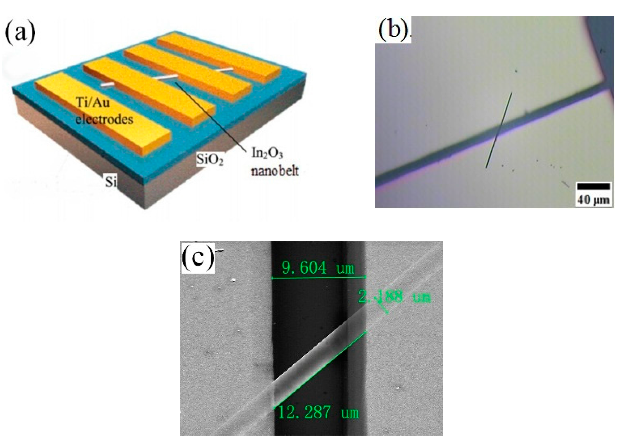
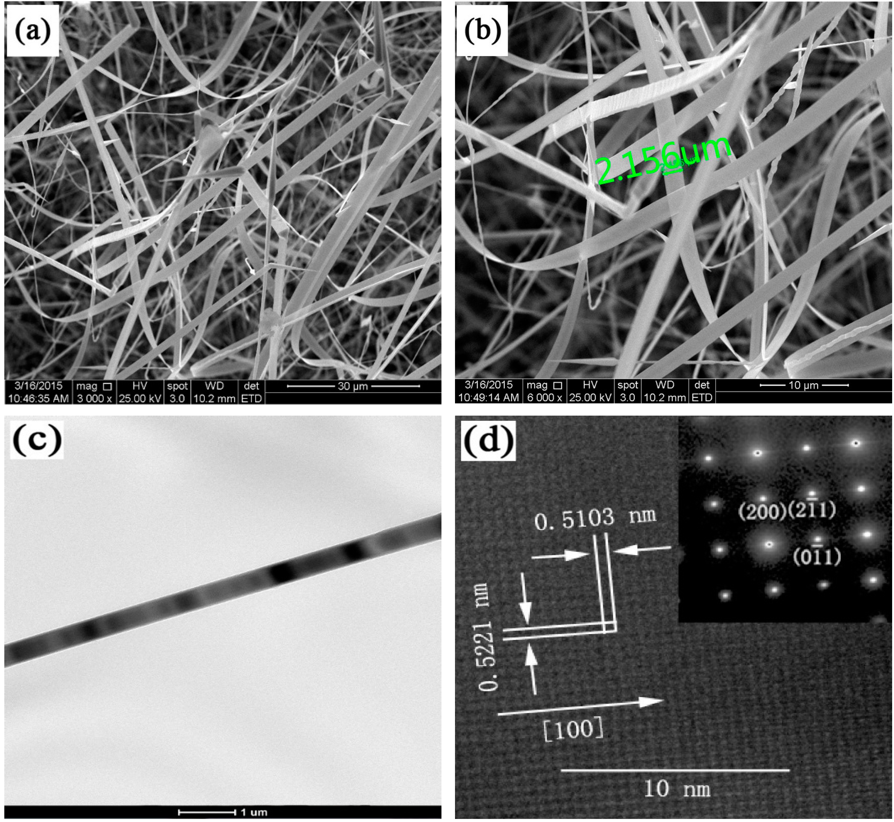
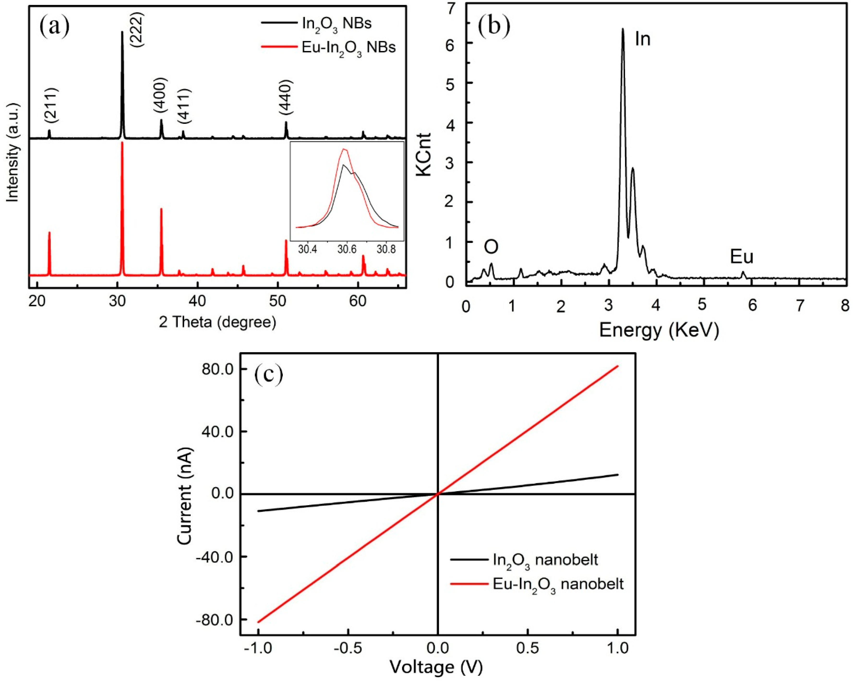
3.1. Structures

SEM images of Eu-In2O3 NBs are presented in Figure 2. It is seen that a large number of NBs were deposited on the substrate in Figure 2a. The length of the obtained NBs reaches several hundred micrometers. Figure 2b is the enlarged image of the local area of Figure 2a and shows that the width with uniform size is about several micrometers. Its surface is smooth and transparent, indicating that the thickness is very thin.
Figure 2. (a) Large-area SEM image; (b) Higher magnification SEM micrograph of Eu-In2O3 NBs; (c) TEM image of Eu-In2O3 NB; (d) HRTEM image, the inset: SAED pattern.
Sensors 15 29775 g002
Figure 2c shows a TEM image of a Eu-In2O3 NB. It reveals that its width is about 480 nm. The HRTEM image and SAED pattern are displayed in Figure 2d and its inset. The interplanar spacings are 0.5221 nm and 0.5103 nm, corresponding to the (2 0 0) and (0 −1 1) crystal planes. The SAED pattern is indexed to the cubic In2O3 structure with a = b = c = 1.011 nm, indicating that it was a single crystal. Comparing HRTEM and SAED images, it is drawn that the growth direction of Eu-In2O3 NBs is along [1 0 1] and and no obvious structural defects exist.
The XRD patterns of Eu-In2O3 and In2O3 NBs are displayed in Figure 3a. It shows that all well-defined diffraction peaks can be indexed as the cubic In2O3 phase with a = b = c = 1.011 nm (JCPDS Card No.06-0416). The prepared sample is well crystallized and no diffraction peaks of other impurities or crystalline by-products are detected. The inset of Figure 3a illustrates that the peak (located at ~30°) of Eu-In2O3 shifts to a lower angle compared with that of In2O3 (at 30.6°), indicating that the constants of the latter are larger than those of the former because the radius of Eu ions (94.7 pm) is larger than that of In ions (80 pm). This result reveals that Eu is doped in the lattice. To further make sure whether Eu is doped into the lattices of In2O3 or not, an energy-dispersive X-ray spectroscopy (EDS) of Eu-In2O3 NBs was carried out, as shown in Figure 3b. It confirms that Eu has been doped into the nanobelts and the content of Eu is 0.86 wt.%. Figure 3c presents I-V curves of the In2O3 NB and Eu-In2O3 NB. It is noted that the curves are nearly linear, revealing that good ohmic contacts are formed between the Eu-In2O3 NB/In2O3 NB and the electrodes. Besides, the resistance of the Eu-In2O3 NB is lower than that of its pure counterpart, indicating that the dopant improves the conductance of the In2O3 NB.
Figure 3. (a) XRD images of Eu-In2O3 and In2O3 NBs and the inset is the position of the peak at 30.6°; (b) EDS pattern of Eu-In2O3 NBs; (c) The I-V curves of the In2O3 NB and Eu-In2O3 NB.
Sensors 15 29775 g003

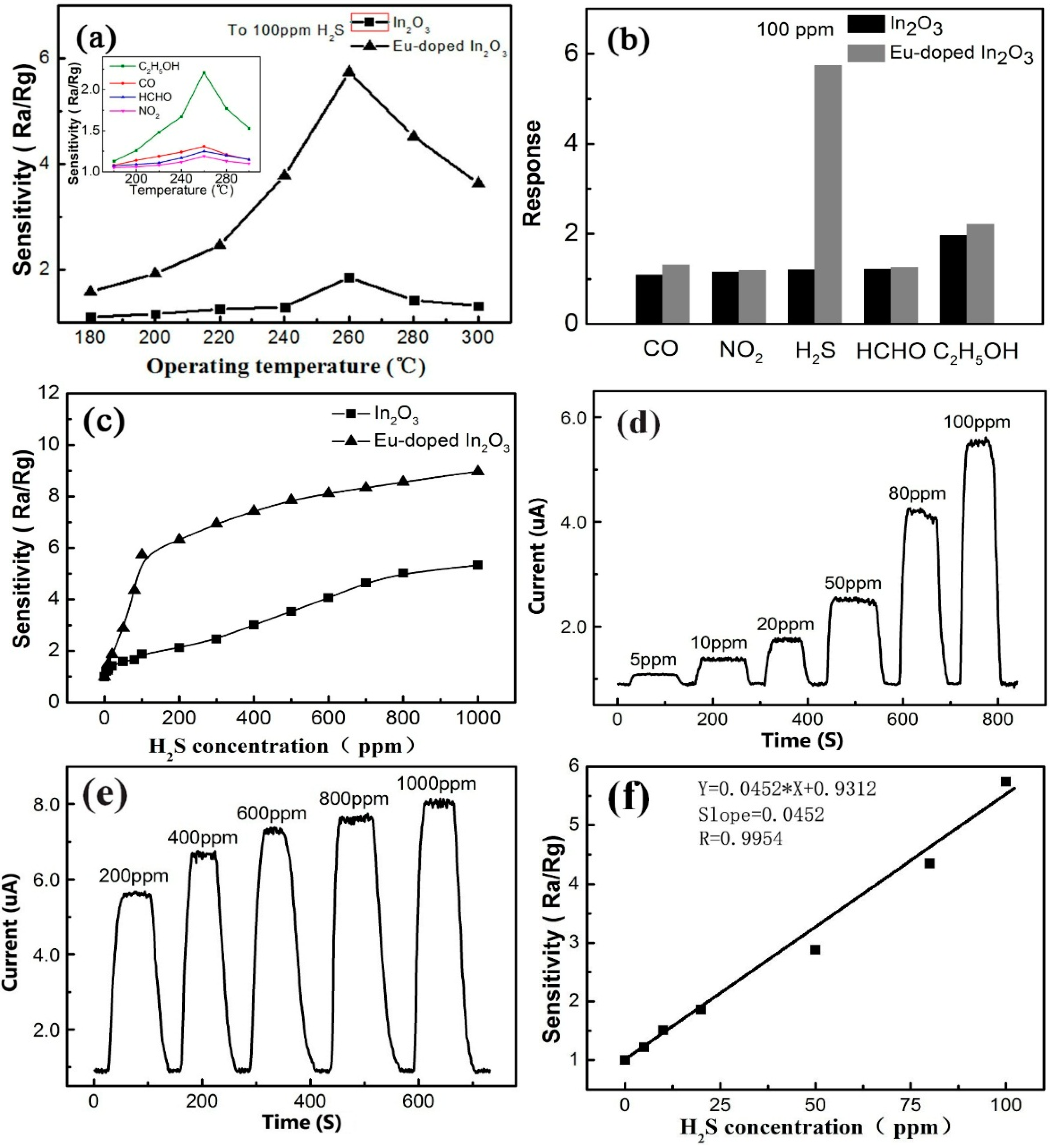
3.2. Sensing Properties

The sensitivity is defined as Ra/Rg where Ra is the sensor resistance in the air and Rg is the resistance in the tested gas or Rg/Ra at an oxidizing one. Figure 4a shows the sensitivity curves of the Eu-In2O3 NB and In2O3 NB to 100 ppm of H2S at different temperatures and its inset shows the sensitivity curves of the Eu-In2O3 NB to different gases at different temperatures. It is obvious that the optimum operating temperatures of the two devices to five tested gases are 260 °C. Furthermore, the response of the Eu-In2O3 device to H2S reaches 5.74, which is five times that of its pure counterpart. The histogram of two devices corresponding to different gases at 260 °C is shown in Figure 4b. The responses to 100 ppm of CO, NO2, HCHO, and C2H5OH at 260 °C are only 1.31, 1.25, 1.19, and 2.21, respectively. The response to H2S is several times higher than that of the other four gases, meaning this sensor is more sensitive to hydrogen sulfide. It is noted that the doping of Eu obviously improves the response to H2S. Although it also increases the responses to other gases, they are not outstanding compared to H2S.
Figure 4. (a) The sensitivity curves of Eu-In2O3 NB and In2O3 NB to 100 ppm of H2S at different temperatures and the inset is the sensitivity curves of Eu-In2O3 NB to different gases at different temperatures; (b) Histogram of two devices responding to different gases at 260 °C; (c) Response curves of Eu-In2O3 NB to H2S at 5~1000 ppm at 260 °C; (d) Responses curve of Eu-In2O3 NB to H2S at 5~100 ppm at 260 °C; (e) Response curve of Eu-In2O3 NB to 200~1000 ppm of H2S at 260 °C; (f) Fitting the curve of response versus H2S concentration in the range of 5–100 ppm.
Sensors 15 29775 g004
The responses to different H2S concentrations at 260 °C are tested, as shown in Figure 4c. It is seen that there is a linear relationship between the response and H2S concentrations when the concentration changes from 0 to 100 ppm and from 100 to 1000 ppm. It is noted that the slope of 5 to 100 ppm is higher than that of 100 to 1000 ppm, illustrating that the response increases slowly in this range. The surface coverage tends to saturate and leads to the slope getting smaller at higher concentrations [23] in that the surface coverage of the adsorbed molecules follows the Langmuir isotherm. In our experiment, the minimum detection concentration of the Eu-In2O3 sensor is about 5 ppm to H2S. As reported in the literature, though the minimum detection concentration of In2O3 can reach about several hundred ppb to H2S, the specific surface area of these nanostructures is always much larger [8]. For instance, Zhao et al. have reported the lowest detection concentration limit of a In2O3 nanotube device could reach 500 ppb for H2S, but that device is composed of many nanotubes, not a single one [5].
Figure 4d shows the responses curves of Eu-In2O3 NB to 5~100 ppm of H2S at 260 °C and it is seen that six cycles are recorded, corresponding to 5, 10, 20, 50, 80, and 100 ppm of H2S. It can be seen that the resistance of In2O3 NB declines significantly upon injection of H2S and returns to its original state when H2S is expelled. Response/recovery time is an important parameter for a gas sensor. For 5~100 ppm of H2S, the response (recovery) time of the Eu-In2O3 NB is 9 (11), 11 (11), 13 (14), 10 (13), 12 (18), and 11 (13) s, respectively. Obviously, the response/recovery time changes little with an increase of H2S concentration and is less than 18 s, manifesting fast response speed. In addition, the response curves of the Eu-In2O3 NB to H2S at high concentrations at 260 °C are shown in Figure 4e. Repeated measurements have been carried out at each concentration and the results are stable and reliable, indicating that the nanobelt device possesses good repeatability and stability.
Fitting the curve of response versus H2S concentration in the range of 5–100 ppm is presented in Figure 4f. It can be seen that the slope of the curve is 0.0452 ppm−1 with a fitting quality of R = 0.9954. The sensor noise is calculated by the variation in the relative response in the baseline with help of root-mean-square deviation (RMSD) [24,25]. Then, 120 data points (N) of Figure 4d at the baseline are collected, and the standard deviation (S) is obtained as 0.0932. According to RMSnoise = S 2 / N , RMSnoise is 0.0085 for the H2S sensor. The theoretical detection limit of the sensor is 0.564 ppm based on the signal-to-noise ratio using DL (ppm) = 3 × (RMSnoise/Slope).

3.3. Sensing Mechanism

In2O3 is an n-type semiconductor and free electrons are major charge carriers [26]. The In2O3 NB adsorbs oxygen-negative ions (O2−, and O) resulting from a combination of oxygen molecules and electrons by Equations (1) and (2), which makes the electrical conductivity of In2O3 NB reduce [27,28].
O2 + e → O2
O2 + e → 2O
The following reactions will occur on the surface of it when In2O3 NB is in the strong reducing atmosphere of H2S.
2H2S + 3O2 = 2H2O + 2SO2 + 3e
H2S + 3O = H2O + SO2 + 3e
According to these reactions, the electrons are released, and the conductivity of the nanobelt is enhanced. On one hand, rare earth ions can promote these reactions as a catalyst, leading to the improvement of the sensitivity [29]. On the other hand, the doping of Eu can effectively increase the number of oxygen vacancies because In2O3 NBs belong to an n-type semiconductor and oxygen vacancies usually provide donor states [30,31]. Thus, the electric conductivity of In2O3 NBs enhances.

4. Conclusions

Eu-doped In2O3 NBs and pure In2O3 NBs have been prapared by the carbon thermal reduction method. The sensitive properties of two devices based on a single Eu-In2O3 NB and its undoped counterpart have been measured using various gases at different concentrations and temperatures. It is found that the response of the Eu-In2O3 device to 100 ppm H2S reaches 5.74, which is fivetimes that of its undoped counterpart, at 260 °C. A linear relationship between the response and different H2S concentrations is obtained when the concentration changes from 5 to 100 ppm and from 100 to 1000 ppm. The theoretical detection limit of the Eu-doped In2O3 NB sensor is 0.564 ppm at optimum working temperature. It reveals that the doping of Eu improves the sensing performance of In2O3 NB effectively and Eu-In2O3 NBs have the potential to be fabricated as H2S sensors.

Acknowledgments

The authors would like to acknowledge the help of their teachers and friends. This work was supported by the National Natural Science Foundation (Grant No. 11164034), the Key Applied Basic Research Program of Science and Technology Commission Foundation of Yunnan Province (Grant No. 2013FA035), and Innovative talents of Science and Technology Plan Projects of Yunnan Province (Grant No. 2012HA007).

Author Contributions

Yingkai Liu guided the experiments and revised the paper. Weiwu Chen performed the synthesis of nanobelts, the gas sensitive test, and wrote the paper. Zhaojun Qin and Yuemei Wu carried out the characterization. Shuanghui Li and Peng Ai helped with the data analysis.

Conflicts of Interest

The authors declare no conflict of interest.

References

  1. Xie, P.; Xiong, Q.H.; Fang, Y.; Qing, Q.; Lieber, C.M. Local electrical potential detection of DNA by nanowire-nanopore sensors. Nat. Nanotechnol. 2012, 7, 119–125. [Google Scholar] [CrossRef] [PubMed]
  2. Lu, M.L.; Weng, T.M.; Chen, J.Y.; Chen, Y.F. Ultrahigh-gain single SnO2 nanowire photodetectors made with ferromagnetic nickel electrodes. NPG Asia Mater. 2012. [Google Scholar] [CrossRef]
  3. Liu, X.; Gu, L.L.; Zhang, Q.P.; Wu, J.Y.; Long, Y.Z.; Fan, Z.Y. All-printable band-edge modulated ZnO nanowire photodetectors with ultra-high detectivity. Nat. Commun. 2014, 5, 4007. [Google Scholar] [CrossRef] [PubMed]
  4. Lu, L.; Chen, J.; Wang, W. Wide bandgap Zn2GeO4 nanowires as photoanode for quantum dot sensitized solar cells. Appl. Phys. Lett. 2013, 103. [Google Scholar] [CrossRef]
  5. Zhao, C.H.; Huang, B.Y.; Xie, E.Q.; Zhou, J.Y.; Zhang, Z.X. Improving gas-sensing properties of electrospun In2O3 nanotubes by Mg acceptor doping. Sens. Actuators B Chem. 2015, 207, 313–320. [Google Scholar] [CrossRef]
  6. Zou, X.M.; Wang, J.L.; Liu, X.Q.; Wang, C.L.; Jiang, Y.; Wang, Y.; Xiao, X.H.; Johnny, C.H.; Li, J.C.; Jiang, C.Z.; et al. Rational Design of Sub-Parts per Million Specific Gas Sensors Array Based on Metal Nanoparticles Decorated Nanowire Enhancement Mode Transistors. Nano Lett. 2013, 13, 3287–3292. [Google Scholar] [CrossRef] [PubMed]
  7. Khiabani, P.S.; Hosseinmardi, A.; Marzbanrad, E.; Ghashghaie, S.; Zamani, C.; Keyanpour-Rad, M.; Raissi, B. NO2 gas sensor fabrication through AC electrophoretic deposition from electrospun In2O3 nanoribbons. Sens. Actuators B Chem. 2012, 162, 102–107. [Google Scholar] [CrossRef]
  8. Kaur, M.; Jain, N.; Sharma, K.; Bhattacharya, S.; Roy, M.; Tyagi, A.K.; Gupta, S.K.; Yakhmi, J.V. Room-temperature H2S gas sensing at ppb level by single crystal In2O3 whiskers. Sens. Actuators B Chem. 2008, 133, 456–461. [Google Scholar] [CrossRef]
  9. Sun, X.H.; Hao, H.R.; Ji, H.M.; Li, X.L.; Cai, S.; Zheng, C.M. Nanocasting synthesis of In2O3 with appropriate mesostructured ordering and enhanced gas-sensing property. ACS Appl. Mater. Interfaces 2014, 6, 401–409. [Google Scholar] [CrossRef] [PubMed]
  10. Lai, X.Y.; Wang, D.; Han, N.; Du, J.; Li, J.; Xing, C.J.; Chen, Y.F.; Li, X.T. Ordered arrays of Bead-Chain-like In2O3 Nanorods and their enhanced sensing performance for formaldehyde. Chem. Mater. 2010, 22, 3033–3042. [Google Scholar] [CrossRef]
  11. Singh, N.; Yan, C.Y.; Lee, P.S. Room temperature CO gas sensing using Zn-doped In2O3 single nanowire field effect transistors. Sens. Actuators B Chem. 2010, 150, 19–24. [Google Scholar] [CrossRef]
  12. Singh, N.; Gupta, R.K.; Lee, P.S. Gold-Nanoparticle-Functionalized In2O3 Nanowires as CO Gas Sensors with a significant enhancement in response. ACS Appl. Mater. Interfaces 2011, 3, 2246–2252. [Google Scholar] [CrossRef] [PubMed]
  13. Choi, S.W.; Katoch, A.; Sun, G.J.; Wu, P.; Kim, S.S. NO2-sensing performance of SnO2 microrods by functionalization of Ag nanoparticles. J. Mater. Chem. C 2013, 1, 2834–2841. [Google Scholar] [CrossRef]
  14. Wu, Y.M.; Zhang, H.; Liu, Y.K.; Chen, W.W.; Ma, J.; Li, S.H.; Qin, Z.J. Synthesis and Gas Sensing Properties of Single La-Doped SnO2 Nanobelts. Sensors 2015, 15, 14230–14240. [Google Scholar] [CrossRef] [PubMed]
  15. Bloor, L.G.; Manzi, J.; Binions, R.; Parkin, I.P.; Pugh, D.; Afonja, A.; Blackman, C.S.; Sathasivam, S.; Carmalt, C.J. Tantalum and Titanium doped In2O3 Thin Films by Aerosol-Assisted Chemical Vapor Deposition and their Gas Sensing Properties. Chem. Mater. 2012, 24, 2864–2871. [Google Scholar] [CrossRef]
  16. Shen, X.; Yan, B. A novel fluorescence probe for sensing organic amine vapors from Eu3+ β-diketonate functionalized Bio-MOF-1 hybrid system. J. Mater. Chem. C 2015, 3, 7038–7044. [Google Scholar] [CrossRef]
  17. Hao, Z.M.; Yang, G.C.; Song, X.Z.; Zhu, M.; Meng, X.; Zhao, S.; Songa, S.; Zhang, H.J. A Europium(III) based Metal-Organic Framework: Bifunctional properties related to sensing and electronic conductivity. J. Mater. Chem. A 2013, 2, 237–244. [Google Scholar] [CrossRef]
  18. Yang, H.X.; Wang, S.P.; Yang, Y.Z. Fabrication of metallic ions doped monodispersed porous In2O3 nanospheres. Mater. Lett. 2013, 110, 45–48. [Google Scholar] [CrossRef]
  19. Ghosh, S.; Das, K.; Sinha, G.; Lahtinenb, J.; De, S.K. Bright white light emitting Eu and Tb Co-Doped Monodisperse In2O3 nanocrystals. J. Mater. Chem. C 2013, 1, 5557–5566. [Google Scholar] [CrossRef]
  20. Li, Z.P.; Fan, Y.J.; Zhan, J.H. In2O3 Nanofibers and Nanoribbons: Preparation by Electrospinning and Their Formaldehyde Gas-Sensing Properties. Eur. J. Inorg. Chem. 2010, 2010, 3348–3353. [Google Scholar] [CrossRef]
  21. Ma, J.; Liu, Y.K.; Zhang, H.; Ai, P.; Gong, N.L.; Zhang, Y. Synthesis and high sensing properties of a single Pd-doped SnO2 nanoribbon. Nanoscale Res. Lett. 2014, 9, 1–10. [Google Scholar] [CrossRef] [PubMed]
  22. Hoa, L.T.; Cuong, N.D.; Hoa, T.T.; Khieu, D.Q.; Long, H.T.; Quang, D.T.; Hoa, N.D.; Hieu, N.V. Synthesis, characterization, and comparative gas sensing properties of tin dioxide nanoflowers and porous nanospheres. Ceram. Int. 2015, 41, 14819–14825. [Google Scholar] [CrossRef]
  23. Chen, P.C.; Sukcharoenchoke, S.; Ryu, K.; Arco, L.G.D.; Badmaev, A.; Wang, C.; Zhou, C.W. 2,4,6-Trinitrotoluene (TNT) chemical sensing based on Aligned Single-Walled Carbon Nanotubes and ZnO Nanowires. Adv. Mater. 2010, 22, 1900–1904. [Google Scholar] [CrossRef] [PubMed]
  24. Liu, H.; Li, M.; Voznyy, O.; Hu, L.; Fu, Q.Y.; Zhou, D.X.; Xia, Z.; Sargent, E.H.; Tang, J. Physically Flexible, Rapid-Response Gas Sensor based on Colloidal Quantum Dot Solids. Adv. Mater. 2014, 26, 2718–2724. [Google Scholar] [CrossRef] [PubMed]
  25. Dua, V.; Surwade, S.P.; Ammu, S.; Agnihotra, S.R.; Jain, S.; Roberts, K.E.; Park, S.; Ruoff, R.S.; Manohar, S.K. All-Organic Vapor Sensor using Inkjet-Printed reduced graphene oxide. Angew. Chem. Int. Ed. 2010, 49, 2154–2157. [Google Scholar] [CrossRef] [PubMed]
  26. Yang, W.; Wan, P.; Zhou, X.D.; Hu, J.M.; Guan, Y.F.; Feng, L. An additive-free synthesis of In2O3 cubes embedded into grapheme sheets and their enhanced NO2 sensing performance at room temperature. ACS Appl. Mater. Interfaces 2014, 6, 21093–21100. [Google Scholar] [CrossRef] [PubMed]
  27. Neri, G.; Bonavita, A.; Micali, G.; Rizzo, G.; Pinna, N.; Niederberger, M.; Ba, J.H. Effect of the chemical composition on the sensing properties of In2O3-SnO2 nanoparticles synthesized by a non-aqueous method. Sens. Actuators B Chem. 2008, 130, 222–230. [Google Scholar] [CrossRef]
  28. Li, Y.S.; Xu, J.; Chao, J.F.; Chen, D.; Ouyang, S.X.; Ye, J.H.; Shen, G.Z. High-aspect-ratio single-crystalline porous In2O3 nanobelts with enhanced gas sensing properties. J. Mater. Chem. 2011, 21, 12852–12857. [Google Scholar] [CrossRef]
  29. Qurashi, A.; El-Maghraby, E.M.; Yamazaki, T.; Kikuta, T. Catalyst supported growth of In2O3 nanostructures and their hydrogen gas sensing properties. Sens. Actuators B Chem. 2010, 147, 48–54. [Google Scholar] [CrossRef]
  30. Ma, J.; Liu, Y.K.; Zhang, H.; Ai, P.; Gong, N.L.; Wu, Y.M.; Yu, D.P. Room temperature ppb level H2S detection of a single Sb-doped SnO2 nanoribbon device. Sens. Actuators B Chem. 2015, 216, 72–79. [Google Scholar] [CrossRef]
  31. Zhang, T.; Gu, F.B.; Han, D.M.; Wang, Z.H.; Guo, G.S. Synthesis, characterization and alcohol-sensing properties of rare earth doped In2O3 hollow spheres. Sens. Actuators B Chem. 2013, 177, 1180–1188. [Google Scholar] [CrossRef]

