
A di/dt Detection Circuit for DC Unidirectional Breaker Based on Inductor Transient Behaviour


1
Computer Systems Department, Instituto Tecnologico Superior del Sur de Guanajuato, Uriangato 38980, Mexico
2
Electronics Department, Tecnologico Nacional de México en Celaya, Celaya 38010, Mexico
3
Electronics Department, Cenidet, Cuernavaca 62490, Mexico
*
Author to whom correspondence should be addressed.
Sustainability 2021, 13(16), 9466; https://0-doi-org.brum.beds.ac.uk/10.3390/su13169466
Submission received: 1 June 2021
/
Revised: 1 August 2021
/
Accepted: 16 August 2021
/
Published: 23 August 2021
(This article belongs to the Special Issue Microgrids for E-mobility: Electrical Machines and Drives, Power Conversion and Energy Management)
Abstract
:In this paper, a di/dt detection circuit for DC breaker applications is proposed to provide faster short-circuit and overcurrent fault detection, where DC breakers are required to be designed for unidirectional fault current conditions, which is a challenge regarding DC microgrid applications due to some associated problems such as long periods of fault interruption, complex circuit structure, and low reliability. The proposal, which is based on measurement of di/dt, can detect fault current conditions for different distances from the point of failure, and is suitable to operation in both islanding and grid-connected conditions. The proposed circuit was studied theoretically and experimentally in steady state, as well as under load changes and short circuit conditions to ensure proper operation, making this solution a fast current fault detection solution, which is a significant advantage and requirement in DC microgrid applications.
1. Introduction
Due to the proliferation of distributed energy resources (DERs), microgrids (MGs) are becoming the future of power generation and consumption due to advantages such as operation in grid-connected or islanded modes, reduction in losses, and power quality improvement [1,2,3,4,5]. Mainly, DC MGs are adopted to reduce power processing, ensure better compatibility with DERs, and ensure better stability [6,7,8,9,10].
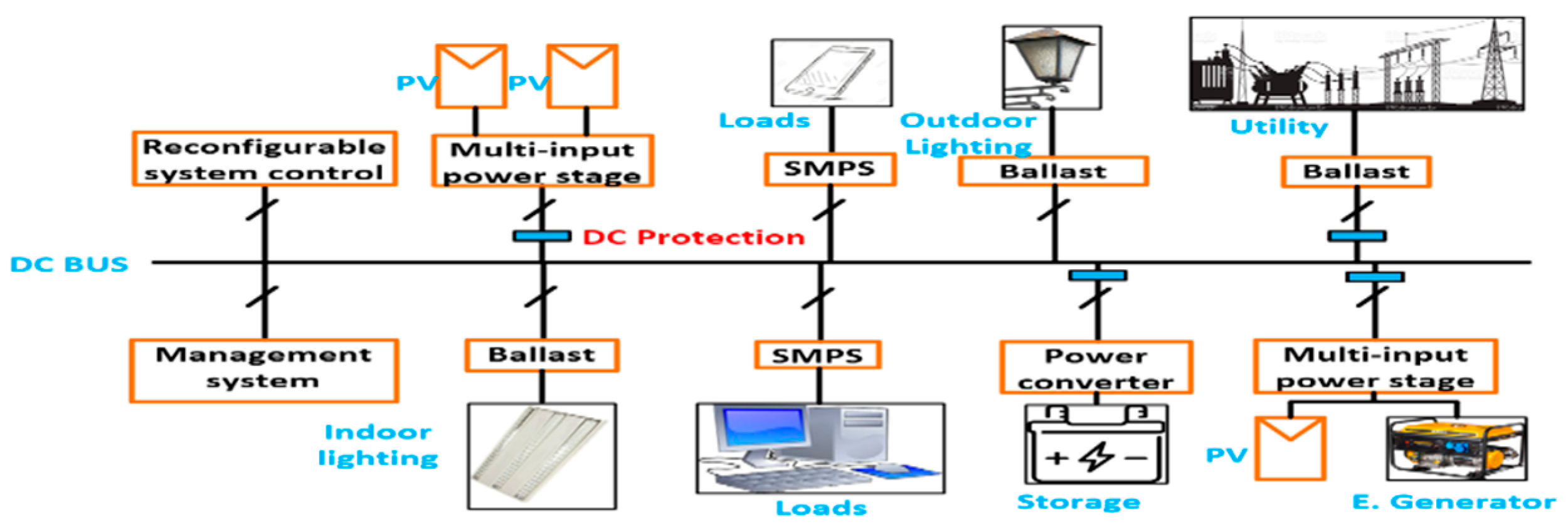
Typical DC microgrid components are loads, renewable sources, storage elements, and bidirectional inverter that acts as the link between the AC grid and the DC bus of the DC MG [11]. Additionally, energy management devices and controllers are required to ensure proper operation [11,12,13,14,15]. As with any electrical system, a DC microgrid is subject to faults; therefore, protection is required [16,17,18]. In Figure 1, an example of a DC microgrid is shown, where DC breakers are placed strategically to prevent a failure due to an electrical fault.
DC breaker design is challenging due to the many aspects considered, such as long periods of fault interruption, complex circuit structure, and low reliability, among others [16,17,18,19]. For example, in terms of protection, the unidirectional nature of the fault current must be considered; therefore, the use of AC protection is not possible. Another important aspect to consider in DC breaker design is that the short circuit current level is different when the DC microgrid operates in grid-connected or islanding modes [17,18]. In grid connected mode, the fault current will be high because both the utility and DERs present inside the DC microgrid feed the fault; in such cases, the current level protection must be faster than the AC grid case due to the fault current magnitude and rise-time are high due to ratio of cable inductance in DC microgrid [17]. A communication system is also recommended to provide efficient coordination in the protection system [19].
To increase the DC breaker’s speed, using solid-state breakers based on SiC devices was proposed in [20,21]. This method is independent of the topology or technique employed for the detection.
In [22], the topology for a unidirectional DC breaker based on a thyristor, passive elements, and coupled inductors was proposed. A “Z” sourced topology was proposed in [23,24]; this scheme naturally opens the thyristor when a fault occurs. In [25], a different topology, similar to the “Z” scheme, was proposed and considered a thyristor to open the circuit. In [26], another topology, based on thyristor, was proposed but can operate bidirectionally.
The designs in these topologies are highly dependent on the parasitic elements of the DC grid; thus, a false or missed detection may occur. Additionally, the protection current level is fixed, which means that it is not suitable for operation in both islanding and grid-connected conditions.
Based on the transient phenomena derivative, fault detection was proposed in [27], which results in an effective method by measuring local variables. Another method was proposed in [28], which considered differential measurements, and then multiple points were measured. An algorithm based on a wavelet transform was proposed in [29], which enabled efficient fault detection. A method to estimate the fault distance was proposed in [30], which considered the current’s derivative. These papers only proposed fault-detection methods and did not propose DC breaker technology; however, a low-cost digital platform was required to assure proper detection.
In this paper, we propose a method to detect short circuits and overcurrent faults based on di/dt; the method only considers measurements of bus currents. The proposed scheme enables detection of the fault at different distances along the bus; additionally, changing the protection current level is possible. It is suitable to operate in both islanding and grid-connected conditions, although it is recommended that a communication system be included. Our proposal offers fast fault detection, and an analogue comparator or a microcontroller may be employed to assure the speed. A TMS320F28379D microcontroller from Texas Instruments was employed to attain the advantages of this tool. The proposed circuit was analysed, designed, and simulated; experimental results are also given to verify the proposal’s performance.
2. Proposed Topology
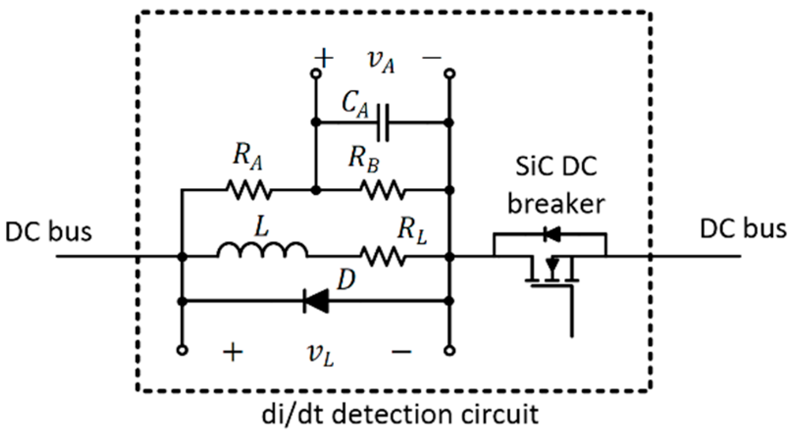
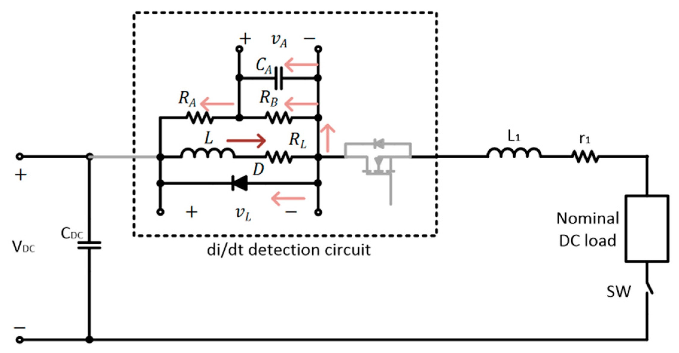
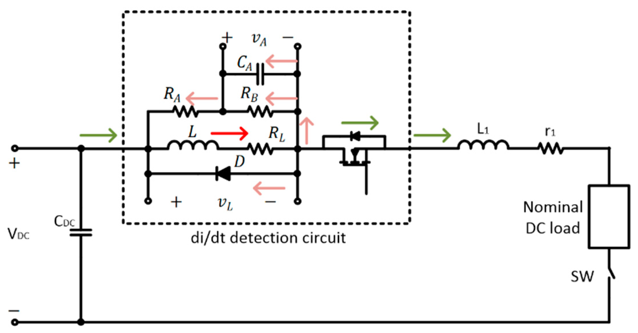
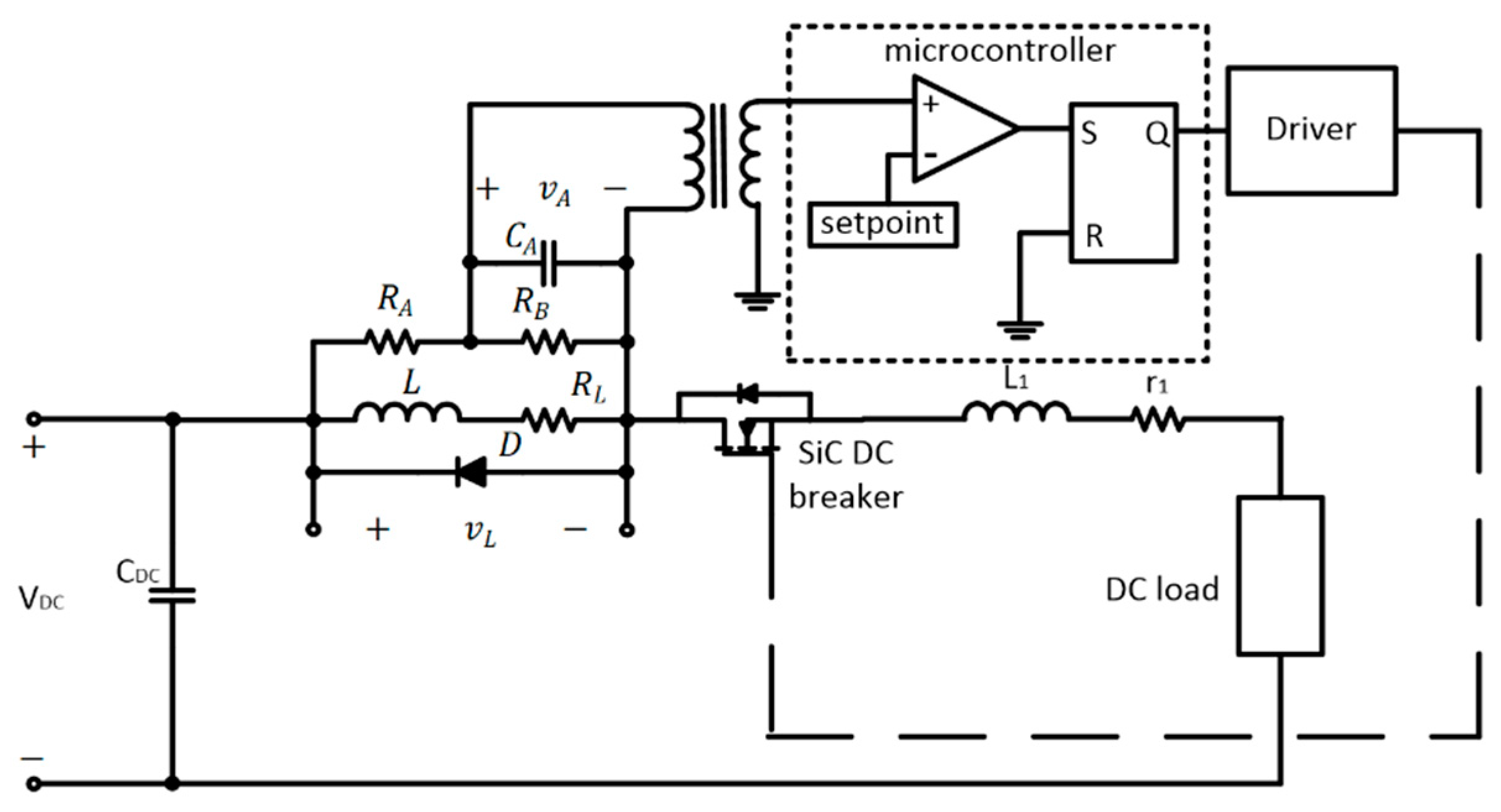
The proposed di/dt detection circuit is shown in Figure 2. The circuit determines whether there is a fault and protects; an analogue filter and a SiC device are employed as the breaker, and a diode (D) is included as protection element to ensure a safe operation when the switch is turned off.
The proposed circuit detects short-circuits faults; however, false detection may occur when the load is varied and if the protection is not designed correctly. Thus, a design methodology is proposed. Considering that large load variation is a natural behaviour of DC microgrids, the following load changes were analysed, from 50% to 100%, 100% to 50%, 0% to 100% nominal load, and from 100% nominal load to short circuit.
The filter output () was compared with the setpoint that specified the di/dt protection level; this signal can be fixed or changed to operate properly in either islanding or grid-connected modes and for different currents demanded.
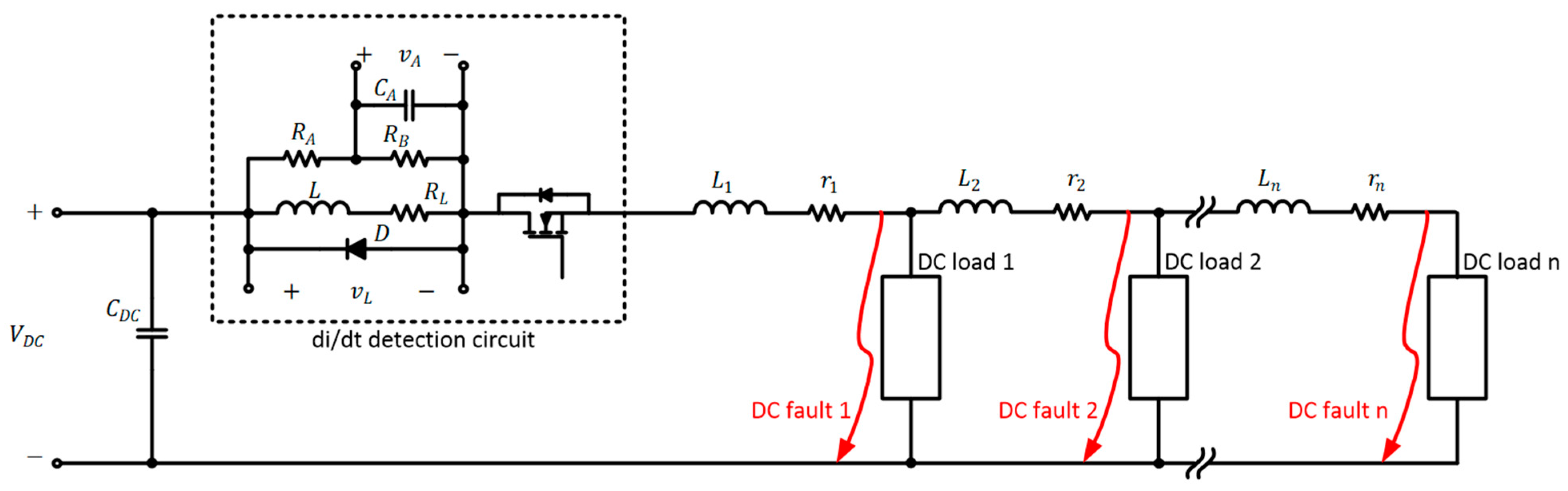
The complete scheme is shown in Figure 3, considering long and short fault distances.
2.1. Transient Inductor Analysis under a Fault
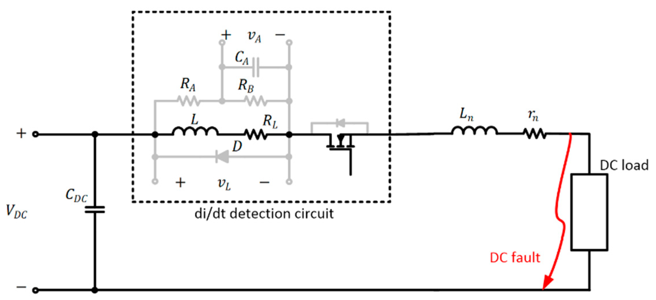
Figure 4 shows the di/dt detection circuit and DC bus under a fault condition, where “n” may determine the distance of the fault according to Figure 3. and are considered as the impedance of the cabling, with the cable impedance being equal for each segment, and the resistor and of the di/dt circuit detection offering a high impedance to avoid coupling.
Applying Kirchhoff’s law, from Figure 4, the following equation can be obtained:
where is the inductance of the breaker, is the inductance of the cabling, is the bus voltage, is the internal resistance of the inductor, is the parasitic resistance of the cabling, is the fault resistance, and is the current of the circuit.
Solving Equation (1) obtains:
where i(0) is the initial current, just before the fault, and:
The inductor voltage is determined by:
Considering Equation (4), the inductor voltage is proportional to the inductor current change, and by substituting Equation (2) into Equation (4) and simplifying, an equation for the inductor voltage under a fault can be obtained:
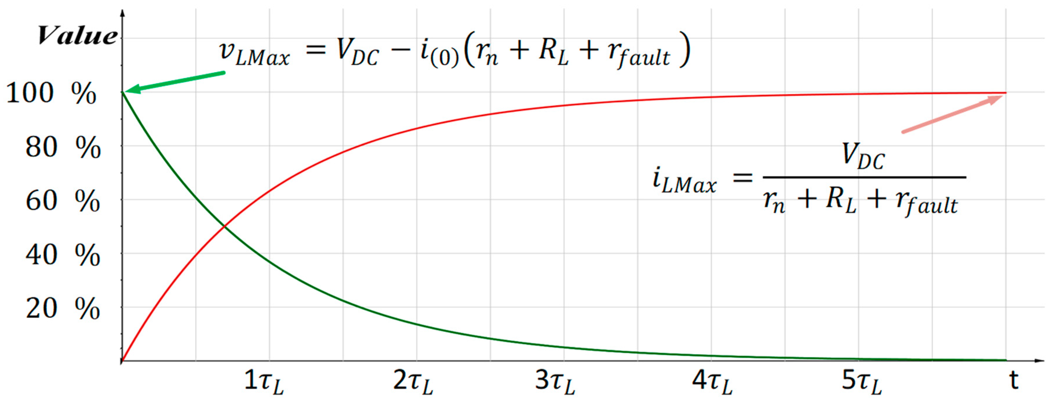
Figure 5 shows the transient behaviour of the current and voltage inductor L, where is the time-constant that determines when the variables reach their final value, which was approximately five time-constants. It can be considered that in a half time-constant, the exponential function exhibits linear behaviour.
The maximum voltage for the inductor is:
The maximum current for the inductor is:
2.2. Transient Analogue Filter Analysis under a Fault
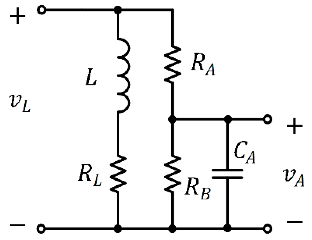
Two critical cases can be considered when a fault occurs at a short and/or long cabling distance, and this is because the short-circuit current is different in each case. If the inductor voltage is considered linear, the detection time must be lower than half of a time-constant in any case. An analogue filter was employed to determine the voltage protection; the simplified circuit is shown in Figure 6.
The behaviour of this circuit is determined by the following equation:
where , , are the elements of the analogue filter, and is the output of the DC breaker.
Solving Equation (8) obtains:
where is the initial voltage, just before the fault, and:
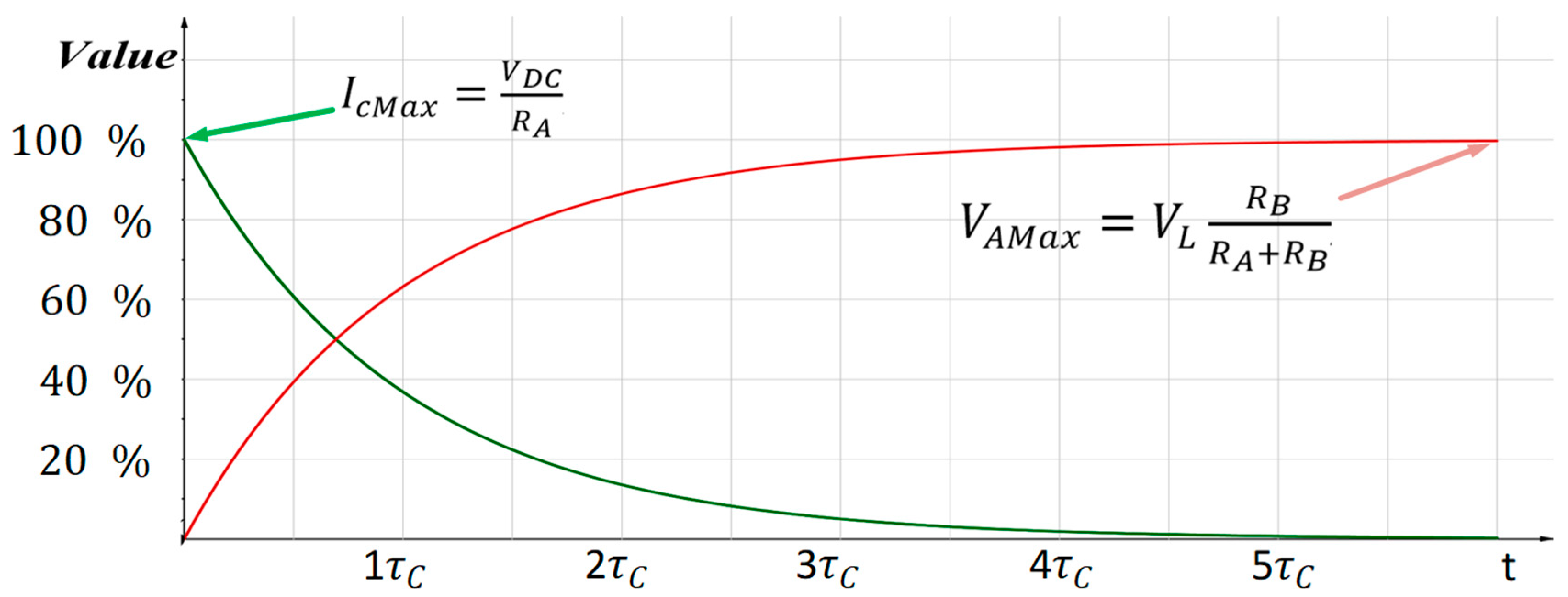
Figure 7 shows the behaviour of the capacitor.
The maximum current of the capacitor is:
The maximum voltage for the capacitor is:
In order to detect short circuits and load changes, the capacitor’s behaviour must be faster than the inductor’s behaviour. For analysis and simplification, the inductor’s behaviour was considered linear until half time-constant , and capacitor behaviour was faster than the inductor behaviour. Thus, the proposition in the following equation is mandatory:
According to Equation (3), when rfault is lower, the time-constant will be higher, which means that the behaviour will be linear for a longer time. To validate Equation (9), which considered VL as constant, the inductor voltage should be considered the average voltage for the inductor voltage, which is given for:
Substituting Equation (5) into Equation (14), considering = 0 and = ½ and simplifying, obtains:
Substituting Equation (6) into Equation (15) and simplifying the following equation is obtained:
Considering that the capacitor’s voltage will be at full load in five time-constants, the following equation is given:
Substituting Equations (10) and (16) into Equation (17) and simplifying, the following equation is obtained:
This equation approximates the analogue filter voltage based on inductor current behaviour to detect a load change and a fault. Then, to decide if a fault occurs, it is just necessary to define the proper value of to trigger the protection as required.
2.3. Analysis under No Load to Full Load Conditions
The system must operate correctly under certain operating conditions, not only in a steady state, but also during load variations. The detection voltage of load variation must also be considered.
The equations previously obtained are still valid with some considerations, such as i(0) = 0, = 0 and substituting rfault for RNom, Equation (18) becomes:
2.4. Analysis under Load Change
The system must support load variations, and this load was connected near the DC breaker because it has a higher current variation. The equation obtained before are still valid with some considerations; for example, if there are five time-constants of the analogue filter transcurred, then the capacitor will be discharged and can be considered and substituting rfault for REq which is the equivalent resistance of the load, Equation (18) becomes:
2.5. Analysis under Steady State
The system must operate correctly in a steady state. In this case, there is not a current variation; therefore, there is no short-circuit or load change detection due to inexistence. If there is an overcurrent, this can be detected with a current sensor.
2.6. Analysis under Open Breaker State
When level protection is detected, the SiC transistor will be open, with the current path shown in Figure 8. In this case, the inductor’s residual energy is conducted through the diode D and the analogue filter; then, the capacitor is discharged.
2.7. Analysis under Negative di/dt
When a reduction in load occurs in the system, the di/dt in the inductor will be negative; the current path is shown in Figure 9. In this case, the excess current in the inductor is conducted through the diode D and the analogue filter; then, the capacitor is discharged, and the current demanded for load is transported for the SiC transistor.
3. di/dt Circuit Design
Considering the previous equations, the design procedure proposed is as follows:
- Define L based on:
- 2.
- Determine the nominal load with the nominal power and bus DC Voltage:
- 3.
- Obtained τL based on Equation (3), but replace rfault for RNom;
- 4.
- Define the detection voltage ;
- 5.
- In order to define RA and RB, substitute Equation (10) into Equation (19) and using t = 0.5 τL = 5 τC and simplifying, the following equation is obtained:
The recommendation is that and values will be high impedance to avoid primary circuit coupling;
- 6.
- In order to define the capacitor value using Equation (10) and considering Equation (13):
- 7.
- Verify that Equation (13) is still valid with the values selected.
With this procedure, we can determine whether the proposed DC breaker works completely, not forgetting that approximations are calculated and that the current for the protection may have slight variations and depends on the distance between the breaker and the fail.
4. Simulation Results
Using the design parameters presented previously, a scheme was designed for validation through simulation. In Table 1, the parameters considered in the DC microgrid and the designed parameter values are shown.
The DC breaker was designed and evaluated under different circumstances. First, a start from no load to full load was performed to verify if the DC breaker delivered false detections due to a sudden natural start. A second test was conducted to evaluate the performance, considering a load variation from 50% to 100% nominal power. A third test was performed from 100% to 50% from nominal power, and finally, a fault test in nominal power was conducted.
4.1. Test under 0% to 100% Nominal Power
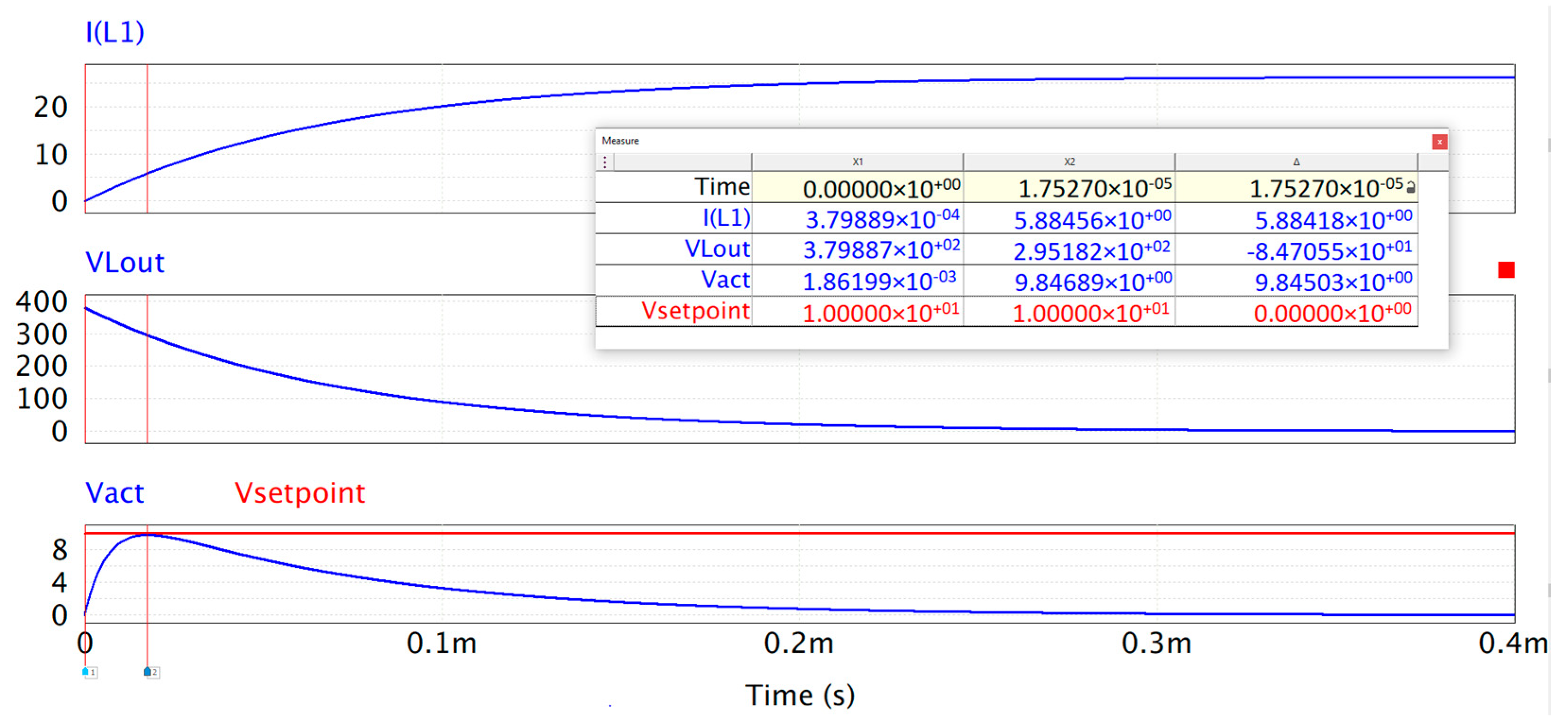
A DC breaker must be able to operate under no load to full load variation; this means that false detection should not occur. Therefore, a test to evaluate this was developed. Figure 10 shows the simulation results, in which a load variation was performed, from no load to full load.
The inductor current, the inductor voltage, and the analogue filter output with the setpoint were graphed. It can be observed that the proposed system operated appropriately, and no false detection occurred. The filter’s output did not reach the setpoint and achieved the maximum value (9.85 V) in approximately 17.5 µs, corresponding to a quarter of the time-constant , and the current reached the maximum value in approximately five time-constants, .
4.2. Test under 20% to 100% Nominal Power
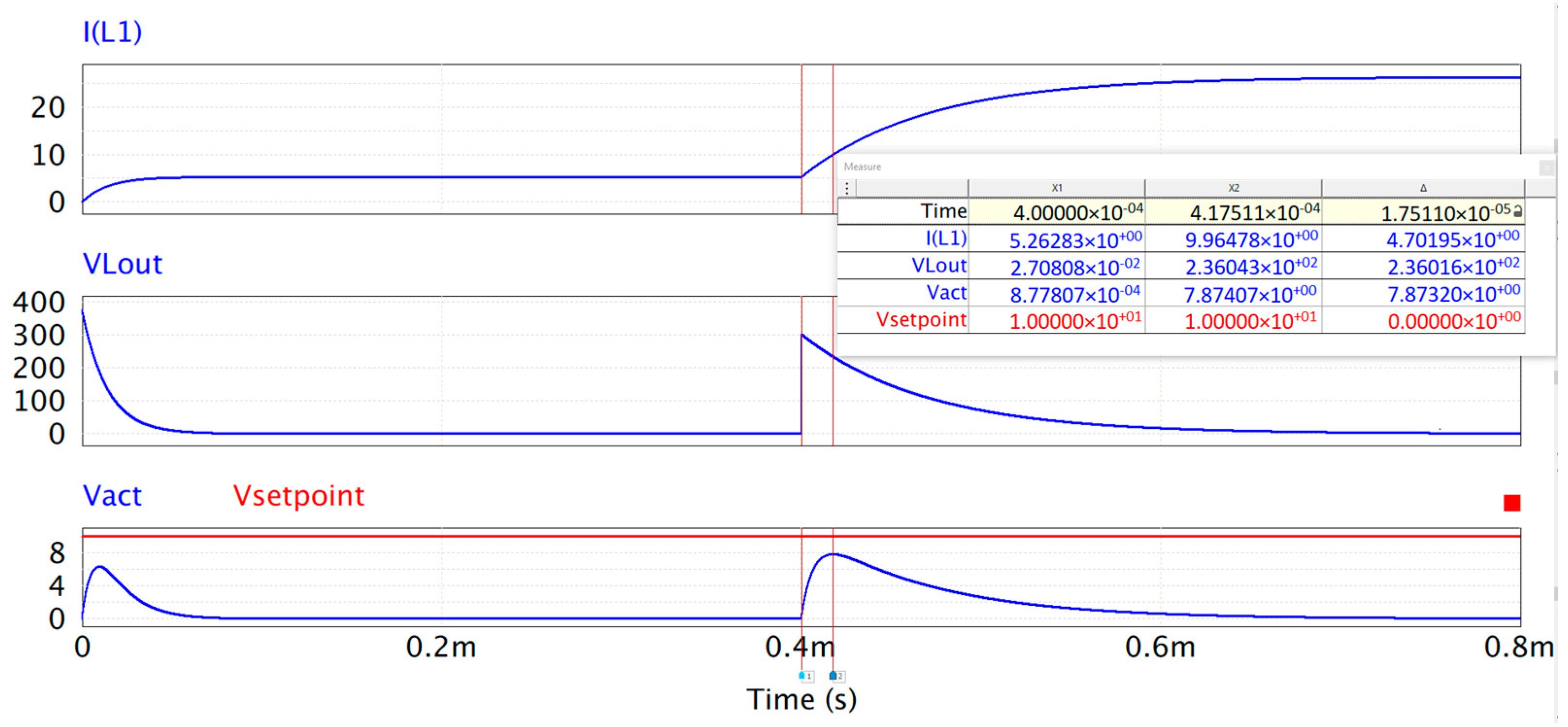
A DC breaker must be able to operate under load variation; this means that false detection should not occur. Therefore, a test was performed to evaluate this. Figure 11 shows the simulation results in which load variation was performed, first from 0% to 20% nominal power and then 400 ms afterwards from 20% to 100% nominal power.
4.3. Test under 100% to 20% Nominal Power
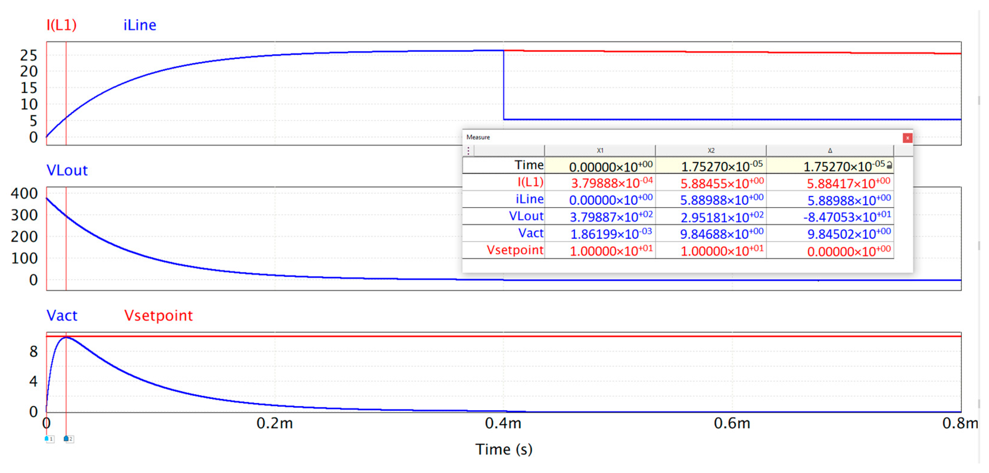
In Figure 12, the simulation results in which a load variation was performed are shown, first from 0% to 100% nominal power and then 400 ms afterwards, from 100% to 20% nominal power.
The inductor and line current, the inductor voltage, and the analogue filter output with the setpoint were graphed. It can be observed that the proposed system operated appropriately, and no false detection occurred; it can also be observed that the line changes from 100% to 20% nominal power, and the residual current of the iL is discharged in diode D and the analogue filter.
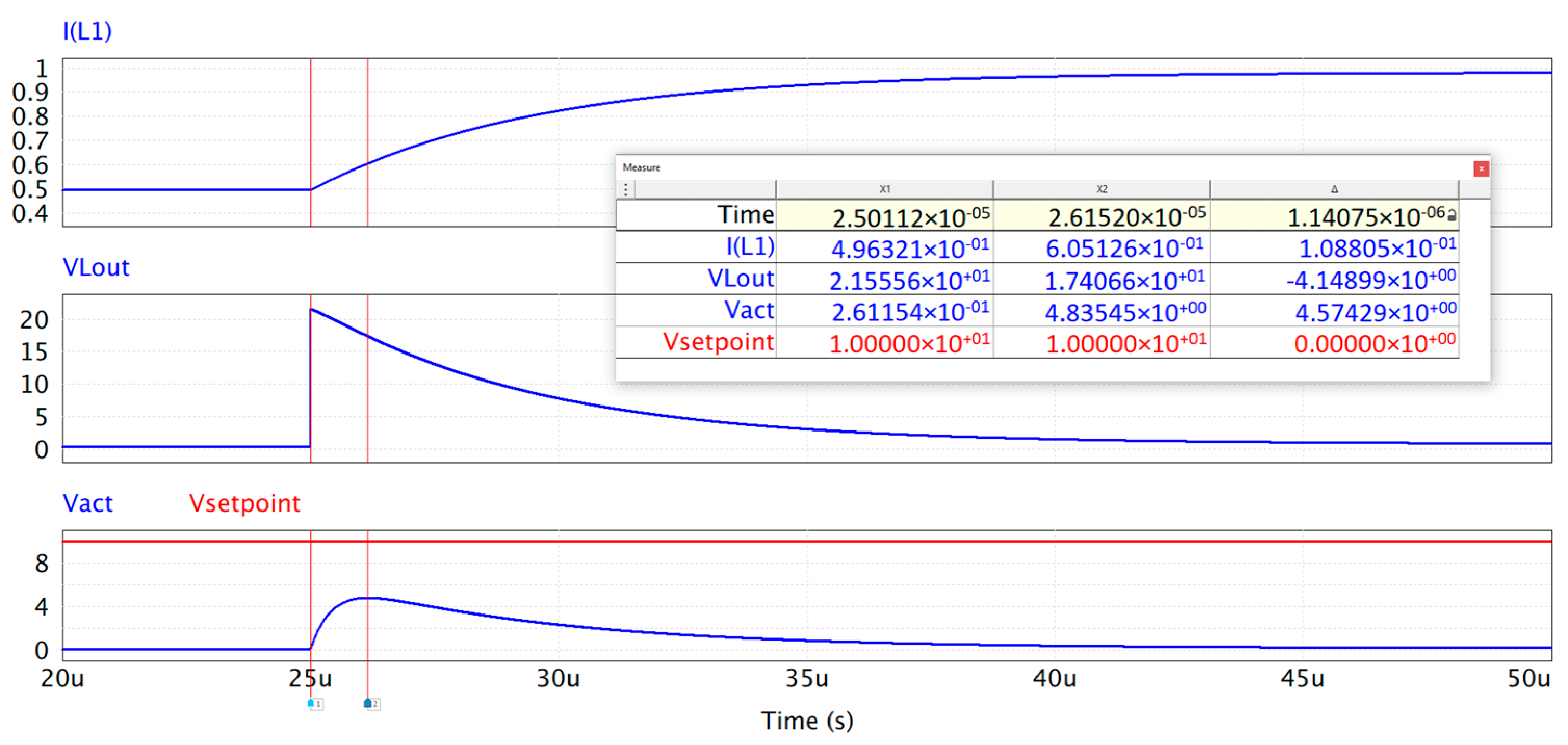
4.4. Test under Nominal Power to Fault
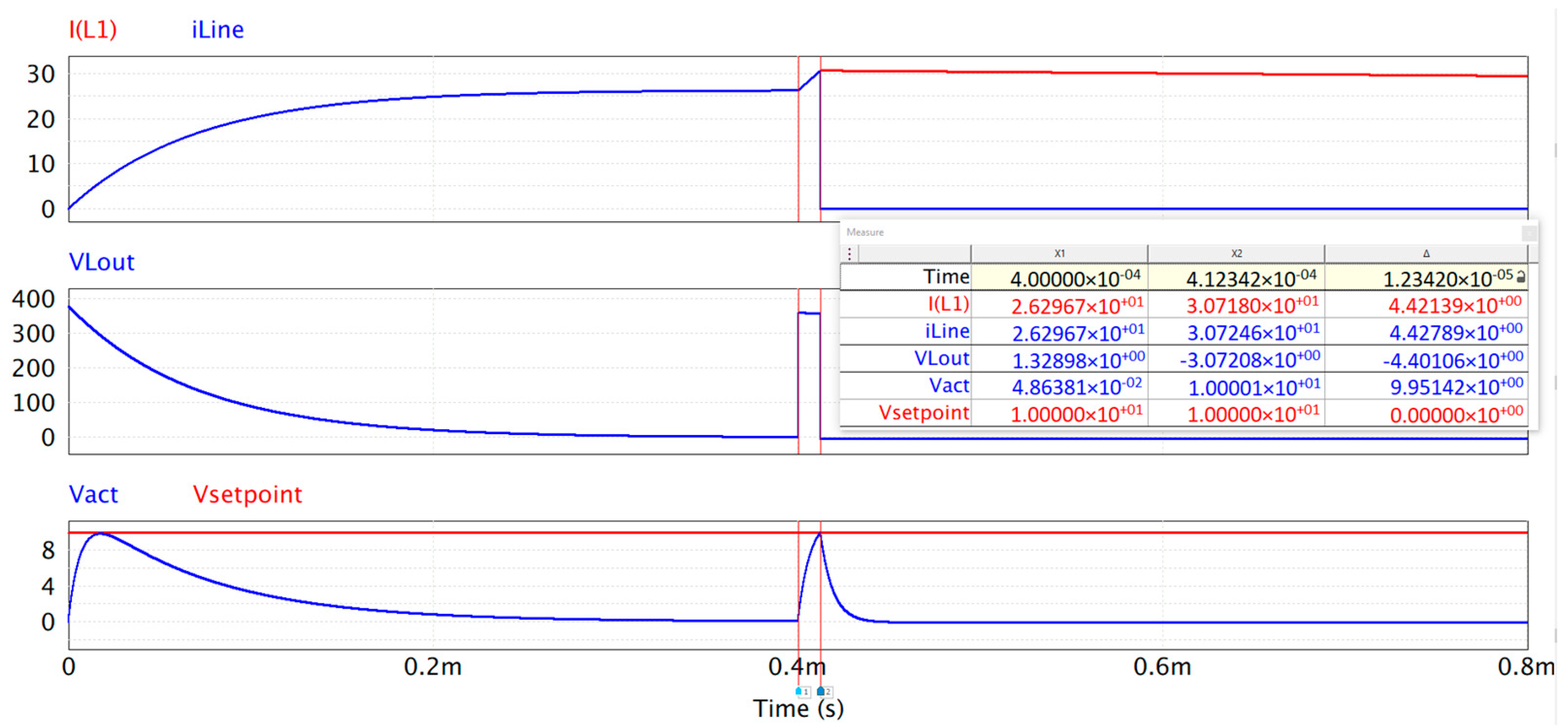
Figure 13 shows the simulation results in which load variation was performed from 100% to fault. The inductor and line current, the inductor voltage, and the analogue filter output with the setpoint were graphed. It can be observed that the proposed system operates appropriately, fault detection occurred, and the line current was protected 12.3 µs after the fault and the current line became zero; then, the iL residual was discharged in diode D.
5. Experimental Results
Using the design parameters presented previously, a scheme was designed for validation in a simulation and experimental test. In Table 2, the parameters considered in the DC microgrid and the designed parameter values are shown. To open the SiC transistor breaker, a microcontroller with a comparator and S-R latch was employed; then, the output filter was connected to a transformer to capture the transient behaviour with a ratio of 5:1 to reduce the voltage, and the microcontroller was capable of handling. The complete scheme is shown in Figure 14.
The DC breaker was designed and evaluated under different circumstances. First, a start from no load to full load was performed to verify whether the DC breaker produced a false detection due to a sudden natural start. A second test was conducted to evaluate the performance considering a load variation from 50% to 100% nominal power. A third test was performed from 100% to 50% from nominal power, and finally, a fault test at nominal power was performed.
5.1. Test under 0% to 100% Nominal Power
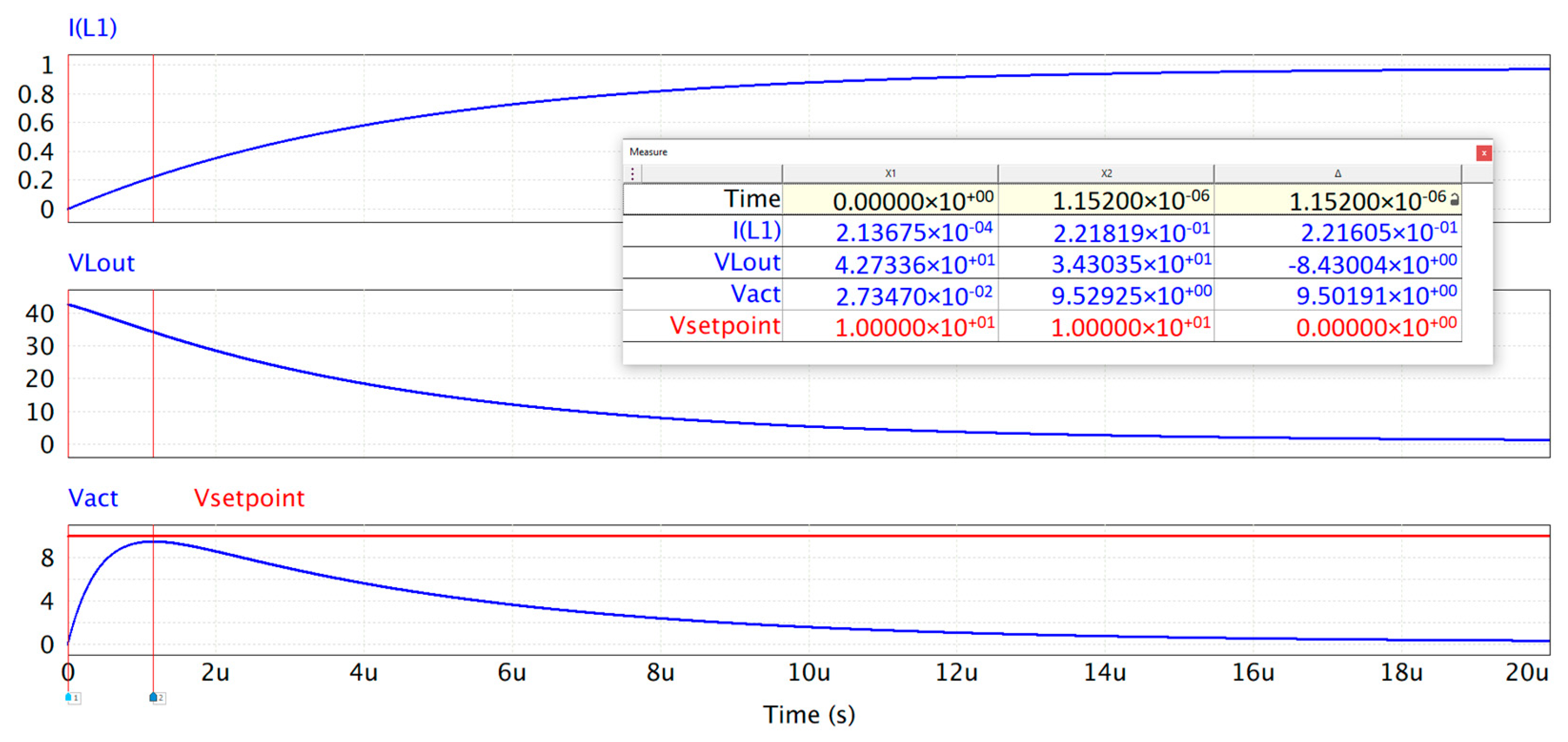
A DC breaker must be able to operate under no load to full load variation; this means that false detection should not occur. Therefore, a test to evaluate this was developed. Figure 15 and Figure 16 show the experimental and simulation results, respectively, in which load variation was performed, from no load to full load.
Figure 15 graphically shows the inductor current, the inductor voltage, and the analogue filter output with the setpoint. It can be observed that the proposed system operated appropriately, and no false detection occurred. The filter’s output did not reach the setpoint and achieved the maximum value approximately in 1 µs, which corresponds to a quarter of the time-constant , and the evolution of the current reached the maximum value approximately five time-constants, .
Figure 16 graphically shows the inductor current, the inductor voltage, and the analogue filter output with the setpoint. It can be observed that the proposed system operated appropriately, as in the simulation, and no false detection occurred. The filter’s output did not reach the setpoint and achieved the maximum value in approximately 1.15 µs, corresponding to a quarter of the time-constant , and the current reached the maximum value in approximately five time-constants .
5.2. Experimental Test under 50% to 100% Nominal Power
A DC breaker must be able to operate under load variation; this means that false detection should not occur. Therefore, a test to evaluate this was developed. Figure 17 and Figure 18 show the experimental and simulation results, in which load variation was performed from 50% to 100% nominal power.
Figure 17 graphically shows the inductor current, the inductor voltage, and the analogue filter output with the setpoint. It can be observed that the proposed system operated appropriately, and no false detection occurred. The filter’s output did not reach the setpoint and achieved the maximum value in approximately 1 µs that corresponding to a quarter of the time-constant , and the current reached the maximum value in approximately five time-constants, .
Figure 18 graphically shows the inductor current, the inductor voltage, and the analogue filter output with the setpoint. It can be observed that the proposed system operated appropriately, as in the simulation, and no false detection occurred. The filter’s output did not reach the setpoint and achieved the maximum value in approximately 1.15 µs, corresponding to a quarter of the time-constant , and the current reached the maximum value in approximately five time-constants, .
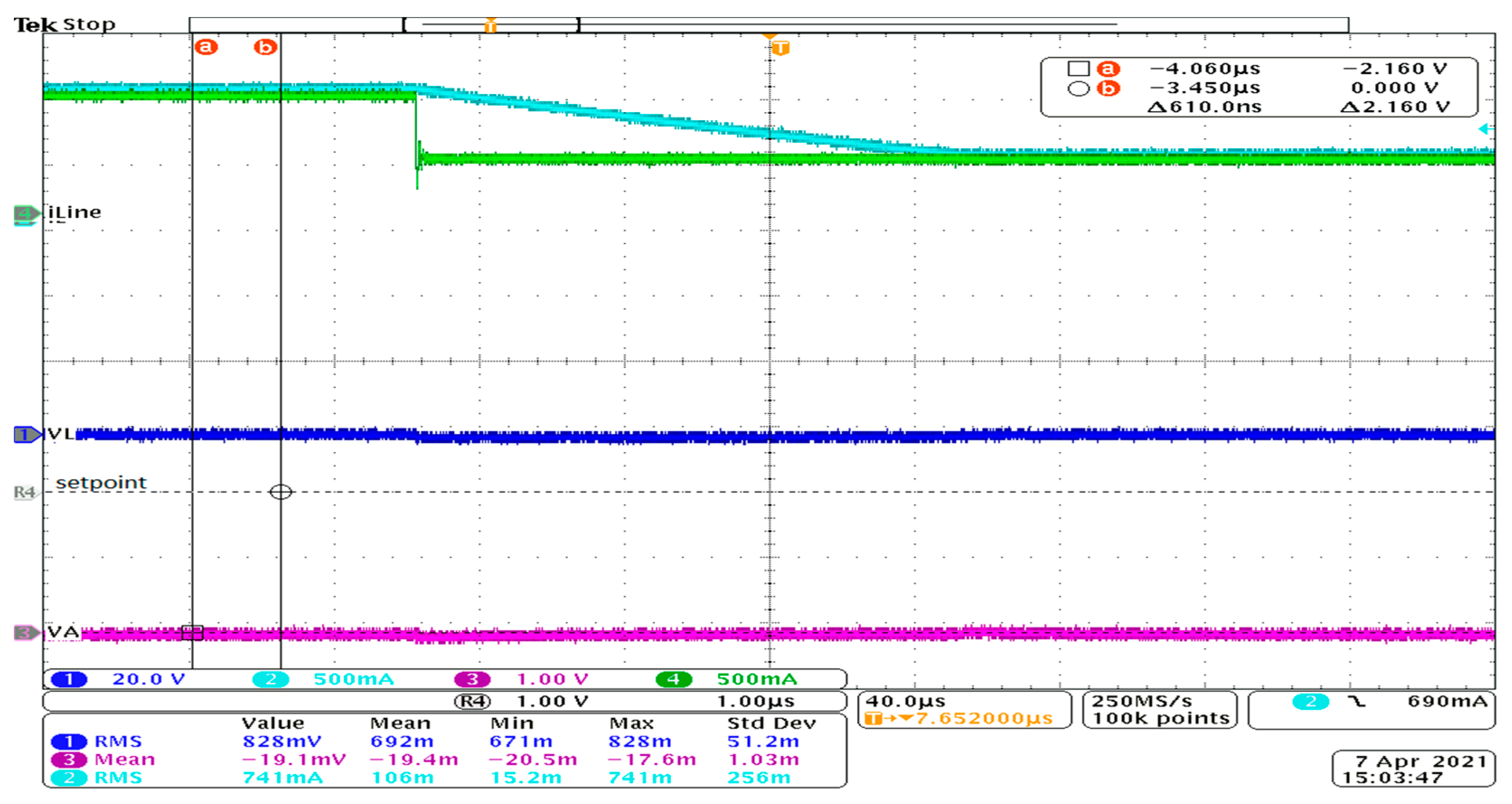
5.3. Experimental Test under 100% to 50% Nominal Power
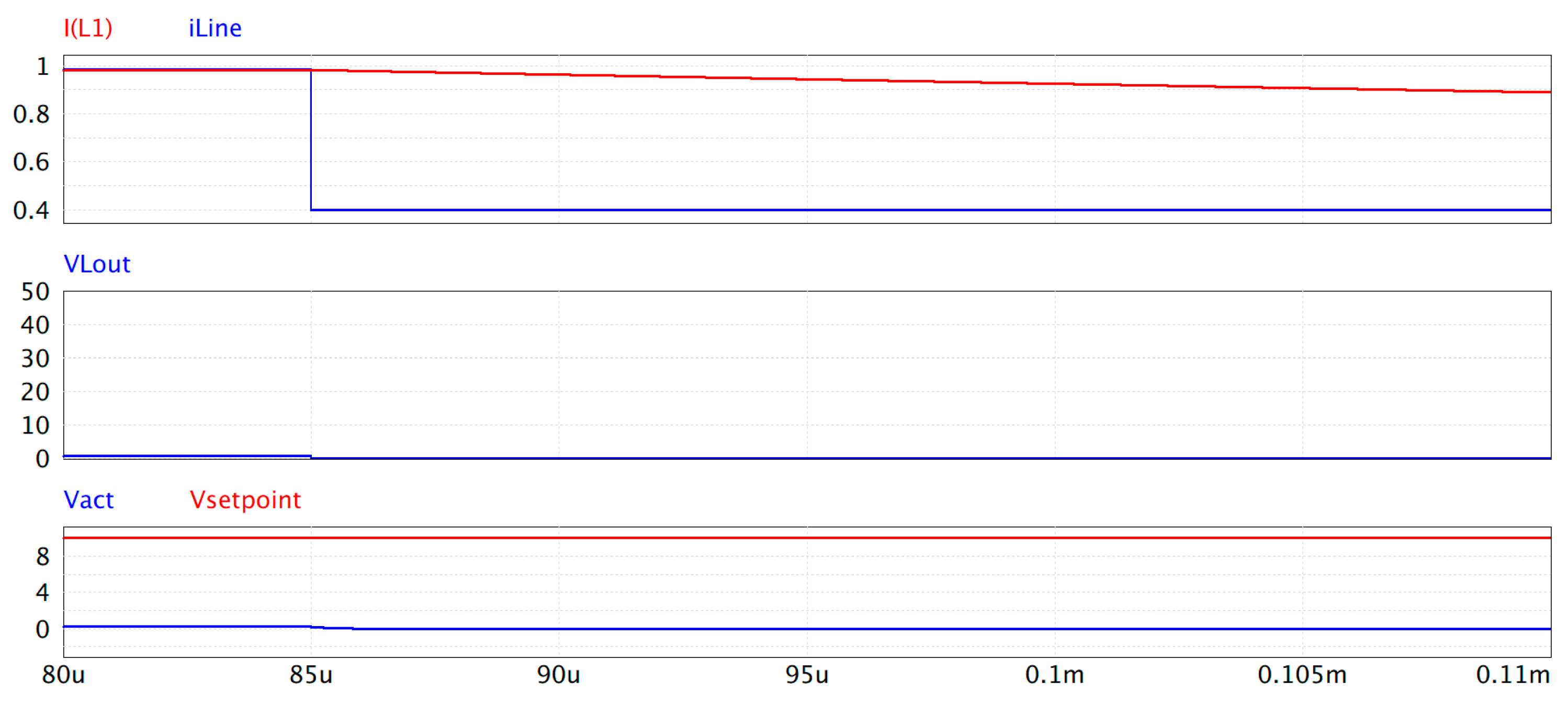
Figure 19 and Figure 20 show the experimental and simulation results, in which a load variation was performed from 100% to 50% nominal power. The inductor and line current, the inductor voltage, and the analogue filter output with the setpoint are graphed.
Figure 19 graphically shows the inductor current, the line current, the inductor voltage, and the analogue filter output with the setpoint. It can be observed that the proposed system operated appropriately, and no false detection occurred. The filter’s output was practically zero, the current inductor residual was discharged into the diode, and the line current changed to 50% as demanded.
Figure 20 graphically shows the inductor current, the line current, the inductor voltage, and the analogue filter output with the setpoint. It can be observed that the proposed system operated appropriately, and no false detection occurred. The filter’s output was practically zero, the current inductor residual was discharged into the diode, and the line current changed to 50% as demanded.
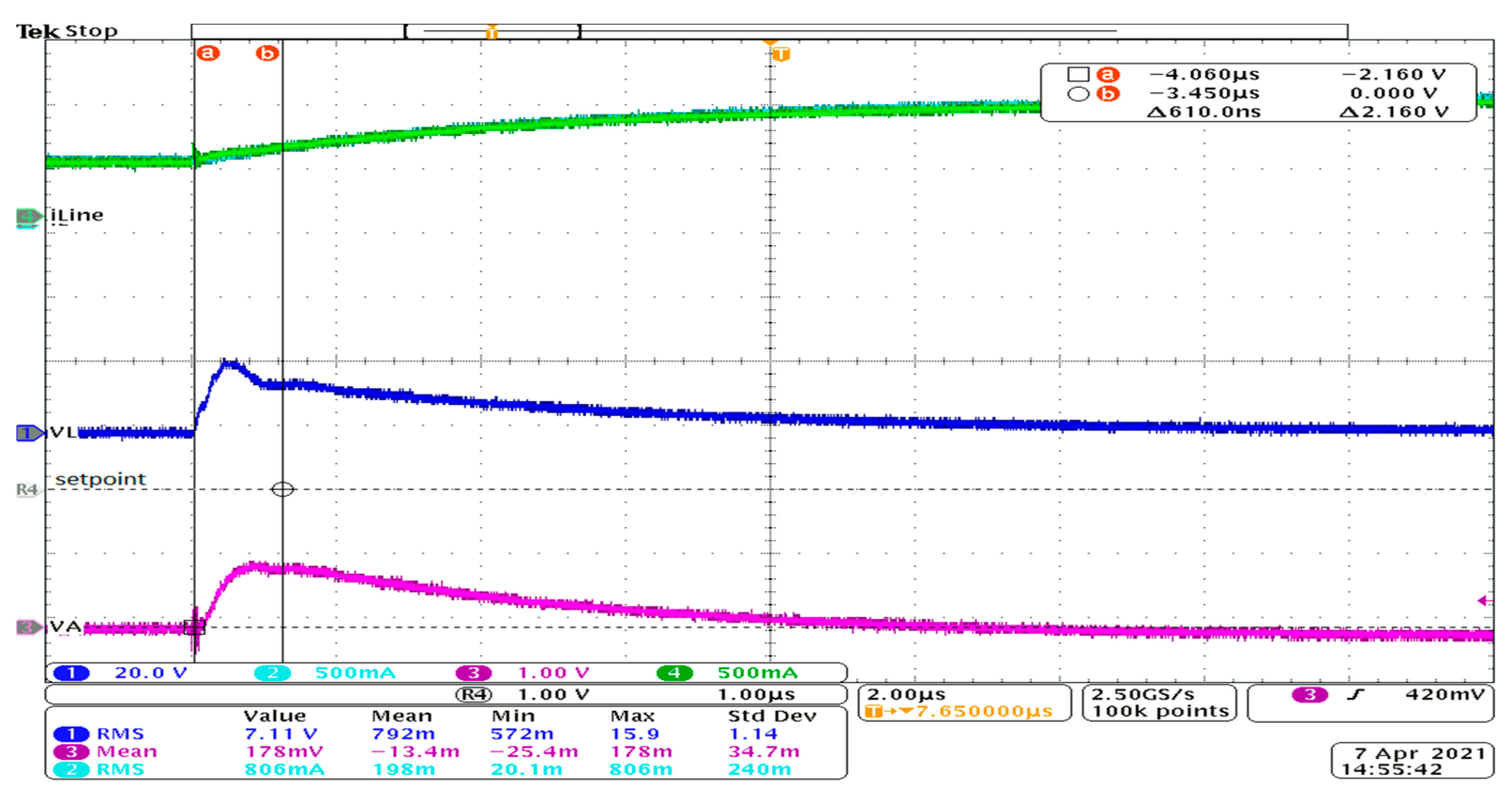
5.4. Test under Nominal Power to Fault
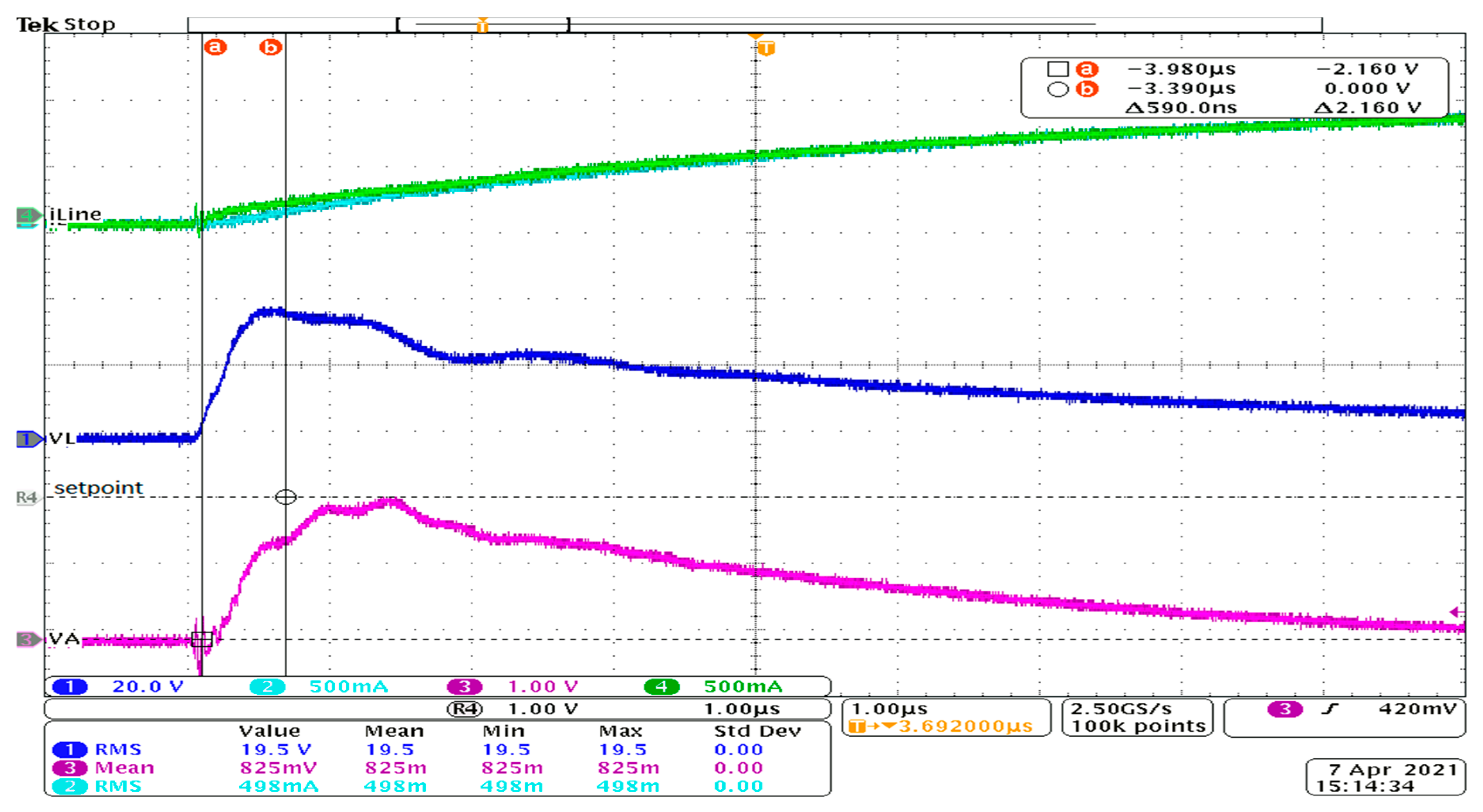
Figure 21 and Figure 22 show the experimental and simulation results in which load variation was performed from 100% to fault. The inductor and line current, the inductor voltage, and the analogue filter output with the setpoint were graphed.
Figure 21 shows the inductor current, the line current, the inductor voltage, and the analogue filter output with the graphed setpoint. It can be observed that the proposed system operated appropriately, detection occurred, and the system was protected. The filter’s output reached the setpoint approximately 0.5 µs, was practically protected in 2 µs, the current inductor residual was discharged into the diode, and the line current changed to zero.
Figure 22 shows the inductor current, the line current, the inductor voltage, and the analogue filter output with the graphed setpoint. It can be observed that the proposed system operated appropriately, detection occurred, and the system was protected. The filter’s output reached the setpoint in approximately 0.5 µs and the system was protected, the current inductor residual was discharged into the diode, and the line current changed to zero.
6. Discussion
A DC microgrid has been suggested as an alternative to increase power efficiency and to handle renewable energy sources. It has several components, including DC protection. In this paper, a DC breaker is proposed to provide faster short-circuit and overcurrent fault detection and is suitable to operation in both islanding and grid-connected conditions.
The proposed system can be appropriately operated under normal conditions without false detection and detects short circuits independently of the DC breaker’s distance. The setpoint can be easily changed to operate in islanding or grid-connected modes, and offers a good alternative to other methods.
The DC breakers are in the research and development stage. The available technologies in the market are bulky, slow, and expensive and are not suitable for a DC microgrid. In the literature are presented several topologies and methodologies to DC protections that are in the research state, and the quantity of the components affect the cost, hence, a proposal with fewer physical components can reduce the cost and be suitable for the market of DC protections.
6.1. A Brief Comparison with Other Methods
In this section, the proposed DC breaker is compared with other methods and circuits; this is illustrated in Table 3. As can be observed, the proposed method is versatile because it is suitable for operation in islanding and grid-connected modes and the protection level can be adjusted by design; this characteristic may also be possible for more complex systems, although this is not clear and has not been mentioned in the literature.
Another important aspect in DC protection systems is the insensitivity to the fault distance of the DC breaker; more complex systems can operate appropriately under this circumstance, although the proposed system also does.
The proposed method is also insensitive to load variations. No false detection occurred and the system exhibited excellent performance; therefore, it is suitable for operation correctly in a DC microgrid. The proposed system’s speed is another essential characteristic, which only a few other methods can match.
6.2. Digital Platform
In addition to the analogue devices shown in Figure 2, for the DC breaker, a microcontroller is suggested to compare the setpoint with the measured voltage, , and then to turn off the breaker. The microcontroller will enable communication with the DC microgrid management system, whereby the setpoint can be changed according to the island or grid mode, and can also be changed to rapidly detect an overcurrent. In addition, if no setpoint has changed, then an OR gate connected to a comparator with a current sensor can be implemented to avoid an overcurrent.
In order to provide a short-circuit and overcurrent fault detection A comparator and a flip-flop analogue should be used. If a microcontroller is considered, then it must have a comparator circuit. In addition, the microcontroller may have a communication protocol for management of the microgrid; a CAN protocol is suggested because it has a bit rate up to 1 Mbps. The bandwidth may have less depending on the type of control strategy used; the main strategies are centralised, decentralised, and hierarchical control—of these, centralised control requires the greatest speed in communication.
7. Conclusions
In this paper, a di/dt detection circuit for a DC unidirectional breaker based on inductor transient behaviour was analysed, and a design methodology and simulations were presented. Finally, the performance of the proposal was verified by experiments.
The di/dt circuit rapidly detects load changes and short circuits with a few components and can be improved by adding a current sensor to detect an overcurrent; in addition, the set point can be easily changed to operate in islanding or grid-connected modes.
The presented topology is currently under study in different conditions, such as the bidirectionality for other types of loads and the coordination with other breakers in different scenarios in island and grid-connected modes for a DC microgrid.
Author Contributions
Investigation, J.V.; supervision, E.J.J.R. and N.V.; validation, J.A. All authors have read and agreed to the published version of the manuscript.
Funding
This research was funded by CONACyT and TecNM.
Institutional Review Board Statement
Not applicable.
Informed Consent Statement
Not applicable.
Data Availability Statement
Not applicable.
Acknowledgments
The authors thank CONACyT and TecNM for supporting this research, and the anonymous reviewers and the Academic Editor for providing helpful comments and suggestions to improve the manuscript.
Conflicts of Interest
The authors declare no conflict of interest.
References
- Mohammed, A.; Refaat, S.S.; Bayhan, S.; Abu-Rub, H. AC microgrid control and management strategies: Evaluation and review. IEEE Power Electron. Mag. 2019, 6, 18–31. [Google Scholar] [CrossRef]
- Bouzid, A.M.; Guerrero, J.M.; Cheriti, A.; Bouhamida, M.; Sicard, P.; Benghanem, M. A survey on control of electric power distributed generation systems for microgrid applications. Renew. Sustain. Energy Rev. 2015, 44, 751–766. [Google Scholar] [CrossRef] [Green Version]
- Planas, E.; Andreu, J.; Gárate, J.I.; Martínez de Alegría, I.; Ibarra, E. AC and DC technology in microgrids: A review. Renew. Sustain. Energy Rev. 2015, 43, 726–749. [Google Scholar] [CrossRef]
- Sarangi, S.; Sahu, B.K.; Rout, P.K. A comprehensive review of distribution generation integrated DC microgrid protection: Issues, strategies, and future direction. Int. J. Energy Res. 2020, 45, 5006–5031. [Google Scholar] [CrossRef]
- Kumar, D.; Zare, F.; Ghosh, A. DC microgrid technology: System architectures, AC grid interfaces, grounding schemes, power quality, communication networks, applications, and standardizations aspects. IEEE Access 2017, 5, 12230–12256. [Google Scholar] [CrossRef]
- Yoldaş, Y.; Önen, A.; Muyeen, S.M.; Vasilakos, A.V.; Alan, İ. Enhancing smart grid with microgrids: Challenges and opportunities. Renew. Sustain. Energy Rev. 2017, 72, 205–214. [Google Scholar] [CrossRef]
- Justo, J.J.; Mwasilu, F.; Lee, J.; Jung, J.-W. AC-microgrids versus DC-microgrids with distributed energy resources: A review. Renew. Sustain. Energy Rev. 2013, 24, 387–405. [Google Scholar] [CrossRef]
- Lai, J.; Lu, X.; Yu, X.; Yao, W.; Wen, J.; Cheng, S. Distributed multi-der cooperative control for master-slave-organized microgrid networks with limited communication bandwidth. IEEE Trans. Ind. Inform. 2019, 15, 3443–3456. [Google Scholar] [CrossRef]
- Trinh, P.-H.; Chung, I.-Y. Optimal control strategy for distributed energy resources in a DC microgrid for energy cost reduction and voltage regulation. Energies 2021, 14, 992. [Google Scholar] [CrossRef]
- Pannala, S.; Patari, N.; Srivastava, A.K.; Padhy, N.P. Effective control and management scheme for isolated and grid connected DC microgrid. IEEE Trans. Ind. Appl. 2020, 56, 6767–6780. [Google Scholar] [CrossRef]
- Guerrero, J.M.; Vasquez, J.C.; Matas, J.; de Vicuna, L.G.; Castilla, M. Hierarchical control of droop-controlled AC and DC microgrids—A general approach toward standardization. IEEE Trans. Ind. Electron. 2011, 58, 158–172. [Google Scholar] [CrossRef]
- Hossain, M.; Pota, H.; Issa, W.; Hossain, M. Overview of AC microgrid controls with inverter-interfaced generations. Energies 2017, 10, 1300. [Google Scholar] [CrossRef]
- Tan, K.T.; So, P.L.; Chu, Y.C.; Chen, M.Z. coordinated control and energy management of distributed generation inverters in a microgrid. IEEE Trans. Power Deliv. 2013, 28, 704–713. [Google Scholar] [CrossRef] [Green Version]
- Mahmud, K.; Sahoo, A.K.; Ravishankar, J.; Dong, Z.Y. Coordinated multilayer control for energy management of grid-connected AC microgrids. IEEE Trans. Ind. Appl. 2019, 55, 7071–7081. [Google Scholar] [CrossRef]
- Olivares, D.E.; Mehrizi-Sani, A.; Etemadi, A.H.; Canizares, C.A.; Iravani, R.; Kazerani, M.; Hajimiragha, A.H.; Gomis-Bellmunt, O.; Saeedifard, M.; Palma-Behnke, R.; et al. Trends in microgrid control. IEEE Trans. Smart Grid 2014, 5, 1905–1919. [Google Scholar] [CrossRef]
- Bayati, N.; Hajizadeh, A.; Soltani, M. Protection in DC microgrids: A comparative review. IET Smart Grid 2018, 1, 66–75. [Google Scholar] [CrossRef]
- Brearley, B.J.; Prabu, R.R. A review on issues and approaches for microgrid protection. Renew. Sustain. Energy Rev. 2017, 67, 988–997. [Google Scholar] [CrossRef]
- Hooshyar, A.; Iravani, R. Microgrid protection. Proc. IEEE 2017, 105, 1332–1353. [Google Scholar] [CrossRef]
- Beheshtaein, S.; Cuzner, R.; Savaghebi, M.; Guerrero, J.M. Review on microgrids protection. IET Gener. Transm. Distrib. 2019, 13, 743–759. [Google Scholar] [CrossRef]
- Shen, Z.J.; Sabui, G.; Miao, Z.; Shuai, Z. Wide-Bandgap Solid-State Circuit Breakers for DC Power Systems: Device and Circuit Considerations. IEEE Trans. Electron. Devices 2015, 62, 294–300. [Google Scholar] [CrossRef]
- Miao, Z.; Sabui, G.; Moradkhani Roshandeh, A.; Shen, Z.J. Design and Analysis of DC Solid-State Circuit Breakers Using SiC JFETs. IEEE J. Emerg. Sel. Top. Power Electron. 2016, 4, 863–873. [Google Scholar] [CrossRef]
- Corzine, K.A. A new-coupled-inductor circuit breaker for DC applications. IEEE Trans. Power Electron. 2017, 32, 1411–1418. [Google Scholar] [CrossRef]
- Maqsood, A.; Corzine, K.A. Integration of Z-Source breakers into zonal DC ship power system microgrids. IEEE J. Emerg. Sel. Top. Power Electron. 2017, 5, 269–277. [Google Scholar] [CrossRef]
- Keshavarzi, D.; Ghanbari, T.; Farjah, E. A Z-source-based bidirectional DC circuit breaker with fault current limitation and interruption capabilities. IEEE Trans. Power Electron. 2017, 32, 6813–6822. [Google Scholar] [CrossRef]
- Li, W.; Wang, Y.; Wu, X.; Zhang, X. A novel solid-state circuit breaker for on-board DC microgrid system. IEEE Trans. Ind. Electron. 2019, 66, 5715–5723. [Google Scholar] [CrossRef]
- Wang, Y.; Li, W.; Wu, X.; Wu, X. A novel bidirectional solid-state circuit breaker for DC microgrid. IEEE Trans. Ind. Electron. 2019, 66, 5707–5714. [Google Scholar] [CrossRef]
- Meghwani, A.; Srivastava, S.C.; Chakrabarti, S. A Non-unit protection scheme for DC microgrid based on local measurements. IEEE Trans. Power Deliv. 2017, 32, 172–181. [Google Scholar] [CrossRef]
- Dhar, S.; Patnaik, R.K.; Dash, P.K. Fault detection and location of photovoltaic based DC microgrid using differential protection strategy. IEEE Trans. Smart Grid 2018, 9, 4303–4312. [Google Scholar] [CrossRef]
- Som, S.; Samantaray, S.R. Efficient protection scheme for low-voltage DC micro-grid. IET Gener. Transm. Distrib. 2018, 12, 3322–3329. [Google Scholar] [CrossRef]
- Zhang, L.; Tai, N.; Huang, W.; Wang, Y. Fault distance estimation-based protection scheme for DC microgrids. J. Eng. 2019, 2019, 1199–1203. [Google Scholar] [CrossRef]
Figure 1.
Example of a DC microgrid with DC breaker.

Figure 2.
di/dt detection circuit.

Figure 3.
Complete scheme for long and short fault distances.

Figure 4.
Equivalent circuit of a di/dt detection circuit for a fault.

Figure 5.
Transient behaviour of voltage (green) and current inductor (red).

Figure 6.
Analogue filter.

Figure 7.
Transient behaviour of voltage (red) and current (green) in the capacitor.

Figure 8.
System under SiC Transistor open.

Figure 9.
System with an open SiC transistor.

Figure 10.
Test under no load to full load variation. From top to bottom: inductor current, inductor voltage, and analogue filter output (blue) with setpoint (red).
Figure 10.
Test under no load to full load variation. From top to bottom: inductor current, inductor voltage, and analogue filter output (blue) with setpoint (red).

Figure 11.
Test under 0% to 20% nominal power and from 20% to 100% nominal power variation. From top to bottom: inductor current, inductor voltage, and analogue filter output (blue) with setpoint (red).
Figure 11.
Test under 0% to 20% nominal power and from 20% to 100% nominal power variation. From top to bottom: inductor current, inductor voltage, and analogue filter output (blue) with setpoint (red).

Figure 12.
Test under 0% to 100% nominal power and from 100% to 20% nominal power variation. From top to bottom: inductor current (red) and line current (blue), inductor voltage (blue), and analogue filter output (blue) with setpoint (red).
Figure 12.
Test under 0% to 100% nominal power and from 100% to 20% nominal power variation. From top to bottom: inductor current (red) and line current (blue), inductor voltage (blue), and analogue filter output (blue) with setpoint (red).

Figure 13.
Test under nominal power to fault. From top to bottom: inductor current (red) and line current (blue), inductor voltage (blue), and analogue filter output (blue) with setpoint (red).
Figure 13.
Test under nominal power to fault. From top to bottom: inductor current (red) and line current (blue), inductor voltage (blue), and analogue filter output (blue) with setpoint (red).

Figure 14.
Experimental implementation scheme.

Figure 15.
Experimental test under no load to full load variation. From top to bottom: inductor current, inductor voltage, and analogue filter output with setpoint.
Figure 15.
Experimental test under no load to full load variation. From top to bottom: inductor current, inductor voltage, and analogue filter output with setpoint.

Figure 16.
Simulation results under no load to full load variation. From top to bottom: inductor current, inductor voltage, and analogue filter output with setpoint.
Figure 16.
Simulation results under no load to full load variation. From top to bottom: inductor current, inductor voltage, and analogue filter output with setpoint.

Figure 17.
Experimental test from 50% to 100% nominal power variation. From top to bottom: inductor current, inductor voltage, and analogue filter output with setpoint.
Figure 17.
Experimental test from 50% to 100% nominal power variation. From top to bottom: inductor current, inductor voltage, and analogue filter output with setpoint.

Figure 18.
Simulation results from 50% to 100% nominal power variation. From top to bottom: inductor current, inductor voltage, and analogue filter output with setpoint.
Figure 18.
Simulation results from 50% to 100% nominal power variation. From top to bottom: inductor current, inductor voltage, and analogue filter output with setpoint.

Figure 19.
Experimental test from 100% to 50% nominal power variation. From top to bottom: inductor current (cyan) and line current (green), inductor voltage (blue), and analogue filter output (pink) with setpoint.
Figure 19.
Experimental test from 100% to 50% nominal power variation. From top to bottom: inductor current (cyan) and line current (green), inductor voltage (blue), and analogue filter output (pink) with setpoint.

Figure 20.
Simulation results from 100% to 50% nominal power variation. From top to bottom: inductor current (red) and line current (blue), inductor voltage (blue), and analogue filter output (blue) with setpoint (red).
Figure 20.
Simulation results from 100% to 50% nominal power variation. From top to bottom: inductor current (red) and line current (blue), inductor voltage (blue), and analogue filter output (blue) with setpoint (red).

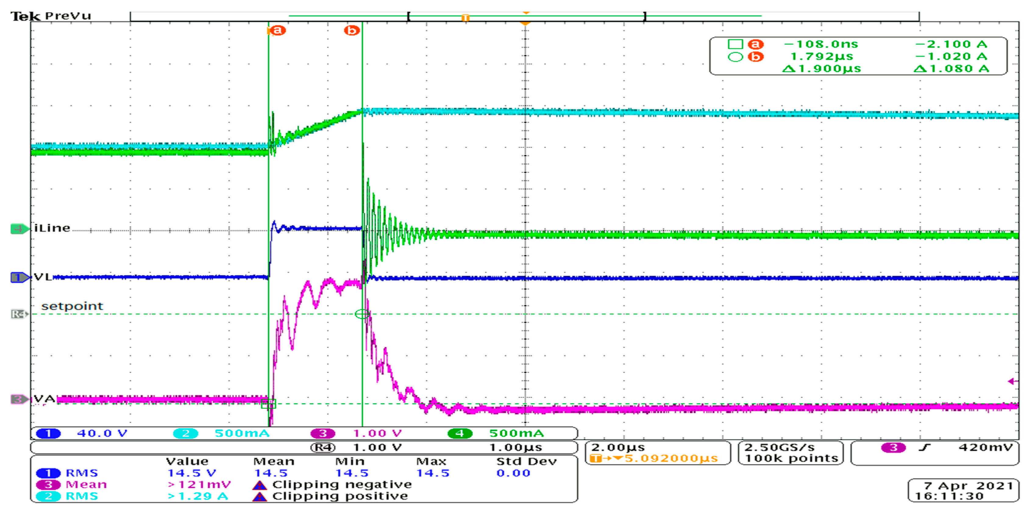
Figure 21.
Experimental test under nominal power to fault. From top to bottom: inductor current (cyan) and line current (green), inductor voltage (blue), and analogue filter output (pink) with setpoint.
Figure 21.
Experimental test under nominal power to fault. From top to bottom: inductor current (cyan) and line current (green), inductor voltage (blue), and analogue filter output (pink) with setpoint.

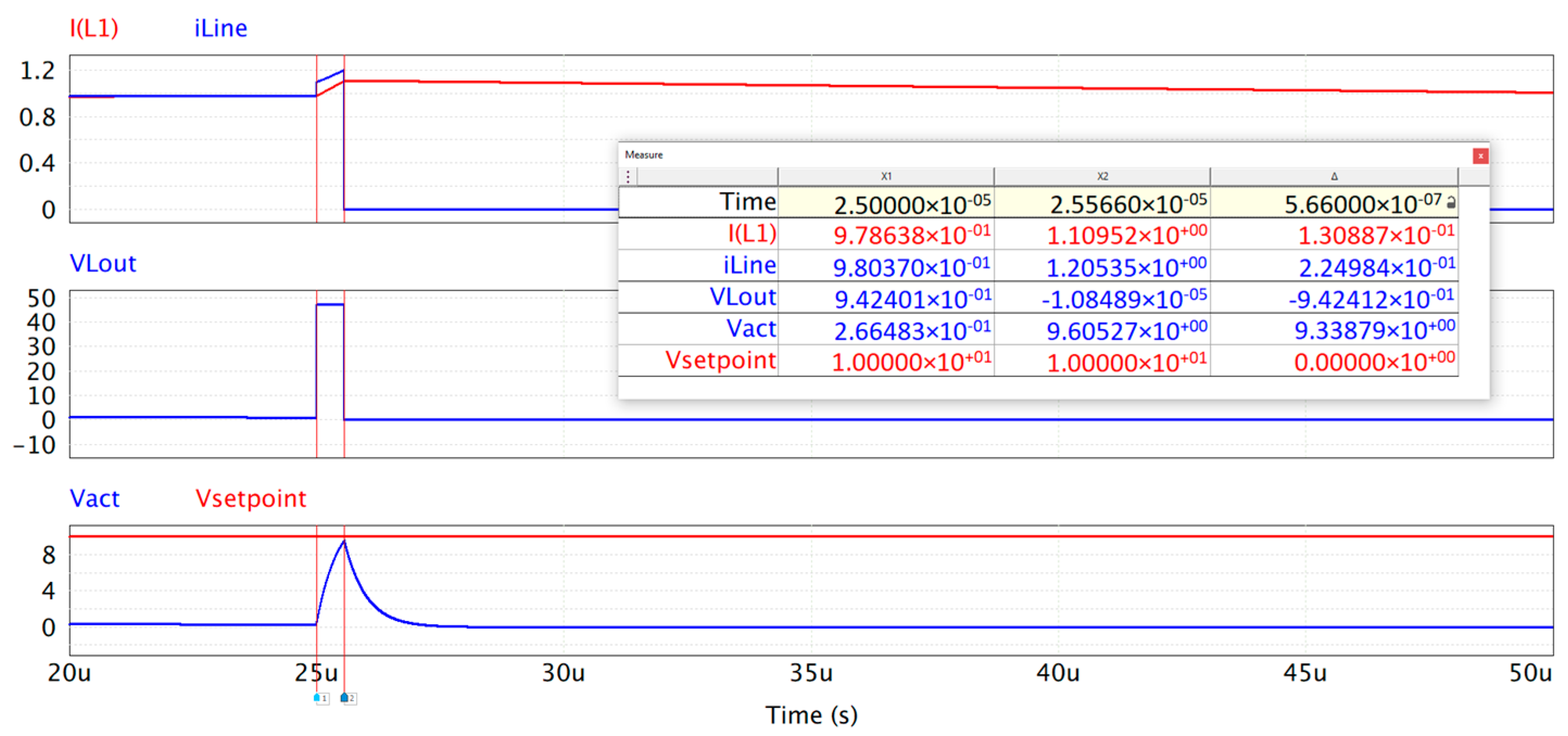
Figure 22.
Simulation results under nominal power to fault. From top to bottom: inductor current (red) and line current (blue), inductor voltage (blue), and analogue filter output (blue) with setpoint (red).
Figure 22.
Simulation results under nominal power to fault. From top to bottom: inductor current (red) and line current (blue), inductor voltage (blue), and analogue filter output (blue) with setpoint (red).


Table 1.
Parameter of the DC microgrid and DC breaker.
| Parameter | Value | Specification |
|---|---|---|
| 10 mΩ | Resistance of cabling | |
| 10 µH | Inductance of cabling | |
| VDC | 380 V | DC bus voltage |
| Rnom | 14.4 Ω | Load under full load |
| Pnom | 10 kW | Nominal power |
| L | 1 mH | Inductance of the DC breaker |
| 5 mΩ | Resistance of Inductor of the DC breaker | |
| 4 nF | Capacitance of the filter | |
| 51 kΩ | Resistance of the filter | |
| 1.76 kΩ | Resistance of the filter | |
| N | Until 20 | Sections of the DC microgrid |
| 10 V | Filter Output Voltage |
Table 2.
Parameter of the experimental test.
| Parameter | Value | Specification |
|---|---|---|
| VDC | 48 V | DC bus voltage |
| Rnom | 48 Ω | Load under full load |
| Pnom | 48 W | Nominal power |
| L | 200 µH | Inductance of the DC breaker |
| 0.2 Ω | Resistance of inductor of the DC breaker | |
| 2.2 nF | Capacitance of the filter | |
| 390 Ω | Resistance of the filter | |
| 150 Ω | Resistance of the filter | |
| 10 V | Filter Output Voltage |
Table 3.
Comparison with other schemes.
| Work | Method | Physical Device Component | Design Complexity | Operating in Islanding and Grid-Mode | Insensitive to Load Variations | Speed |
|---|---|---|---|---|---|---|
| [21] | Self-powered SiC device | Flyback converter, MOSFET, PWM circuit and passive components | High | No | No | 0.5–2 µs |
| [22,23,24,25,26] | Z topology, Thyristor | Thyristor, coupled inductor, and passive components | Medium | No | Not clear | 2–180 ms |
| [27] | Local measurement | Not mention | Medium | Not clear | Yes | 100 µs |
| [28] | Differential measurement | Not mention | Medium | Not clear | Yes | 100 ms |
| [29] | Wavelets | Not mention | Complex | Not clear | Yes | 450 µs |
| [30] | Differential inductor | Not mention | Medium | Not clear | Yes | 5 ms |
| Proposed | di/dt transient | 1 inductor, 1 SiC MOSFET, small passive components and a microcontroller | Low | Yes | Yes | 1.9 µs |
Publisher’s Note: MDPI stays neutral with regard to jurisdictional claims in published maps and institutional affiliations. |
© 2021 by the authors. Licensee MDPI, Basel, Switzerland. This article is an open access article distributed under the terms and conditions of the Creative Commons Attribution (CC BY) license (https://creativecommons.org/licenses/by/4.0/).
Share and Cite
MDPI and ACS Style
Vázquez, J.; Rodriguez, E.J.J.; Arau, J.; Vázquez, N. A di/dt Detection Circuit for DC Unidirectional Breaker Based on Inductor Transient Behaviour. Sustainability 2021, 13, 9466. https://0-doi-org.brum.beds.ac.uk/10.3390/su13169466
AMA Style
Vázquez J, Rodriguez EJJ, Arau J, Vázquez N. A di/dt Detection Circuit for DC Unidirectional Breaker Based on Inductor Transient Behaviour. Sustainability. 2021; 13(16):9466. https://0-doi-org.brum.beds.ac.uk/10.3390/su13169466
Chicago/Turabian StyleVázquez, Jeziel, Elias J. J. Rodriguez, Jaime Arau, and Nimrod Vázquez. 2021. "A di/dt Detection Circuit for DC Unidirectional Breaker Based on Inductor Transient Behaviour" Sustainability 13, no. 16: 9466. https://0-doi-org.brum.beds.ac.uk/10.3390/su13169466
Note that from the first issue of 2016, this journal uses article numbers instead of page numbers. See further details here.